![jasmine - Krishna districtkrishna.nic.in/PDFfiles/MSME/Chemical/jasmine concrete[1].pdfSECTION XI SWOT ANALYSIS ... * Synthite Industrial Chemicals Ltd., ... Jasmine concentrate is](https://static.fdocuments.in/doc/165x107/5aada77e7f8b9aa06a8ea13a/jasmine-krishna-concrete1pdfsection-xi-swot-analysis-synthite-industrial.jpg)
The Jasmine OpenSSD PlatformThe Jasmine OpenSSDb99902075/openSSD/English-copy-of... · The Jasmine...
126
Transcript of The Jasmine OpenSSD PlatformThe Jasmine OpenSSDb99902075/openSSD/English-copy-of... · The Jasmine...
The Jasmine OpenSSD PlatformTheJasmine OpenSSDVersion 1.4
Technical Reference ManualTechnical ReferenceManual
Platform:
Page 2
Copyright 2011 VLDB Lab. All rights Rev.
Version 1.4
Revision historyreserved.Date Author Description20110427 imsangpil (Sungkyunkwan University) Initial release 1.0
20110428 imsangpil (Sungkyunkwan University) fix typo & reflect review comments 1.1
20110520 imsangpil (Sungkyunkwan University) Section 2.1, 2.3, 2.5 update 1.2
20110601 imsangpil (Sungkyunkwan University) fix errata (Section 4.4 & 4.5) 1.3
20120111 imsangpil (Sungkyunkwan 3.3.2)
University)Fix errata & Update some additional information (Section 2.5,
1.4
The Jasmine OpenSSD Platform: Technical Reference ManualThe Jasmine OpenSSD Platform: Technical
Reference Manual
ContentsPREFACE 4A
BOUT THIS
4 CONTENTS 4 F
URTHER
4 FEEDBACK 4
CHAPTER 1. JASMINE OPENSSD PLATFORM SPECIFICATION............................................ 61.1.
6 1.2. JASMINE BOARD 6
CHAPTER 2. INDILINX BAREFOOTTM SSD CONTROLLER SPECIFICATION............................ 82.1.
8 2.2. MEMORY MAP 11 2.3. NAND
15 2.4. SATA CONTROLLER 18 2.5. DRAM H
OST
Page 3
Copyright 2011 VLDB Lab. All rights reserved. C
ONTROLLER
................................................ ...................................... 19 2.6. MEMORY UTILITY 22 2.7. I
NTERRUPT
B
UFFER
&
23
CHAPTER 3. JASMINE OPENSSD PLATFORM FIRMWARE ARCHITECTURE....................... 253.1.
25 3.2. HOST INTERFACE LAYER 25 3.3.
26 3.4. FLASH INTERFACE LAYER 30
CHAPTER 4. JASMINE OPENSSD PLATFORM SOFTWARE SPECIFICATION........................ 324.1.
32 4.2. INSTALLER FUNCTION 34 4.3. FTL P
ROTOCOL
API 35 4.4. LLD API 36 4.5. M
EMORY
U
TILITY
API 40
Version 1.4
The Jasmine OpenSSD Platform: Technical Reference Manual
Page 4
Copyright 2011 VLDB Lab. All rights reserved.
Version 1.4
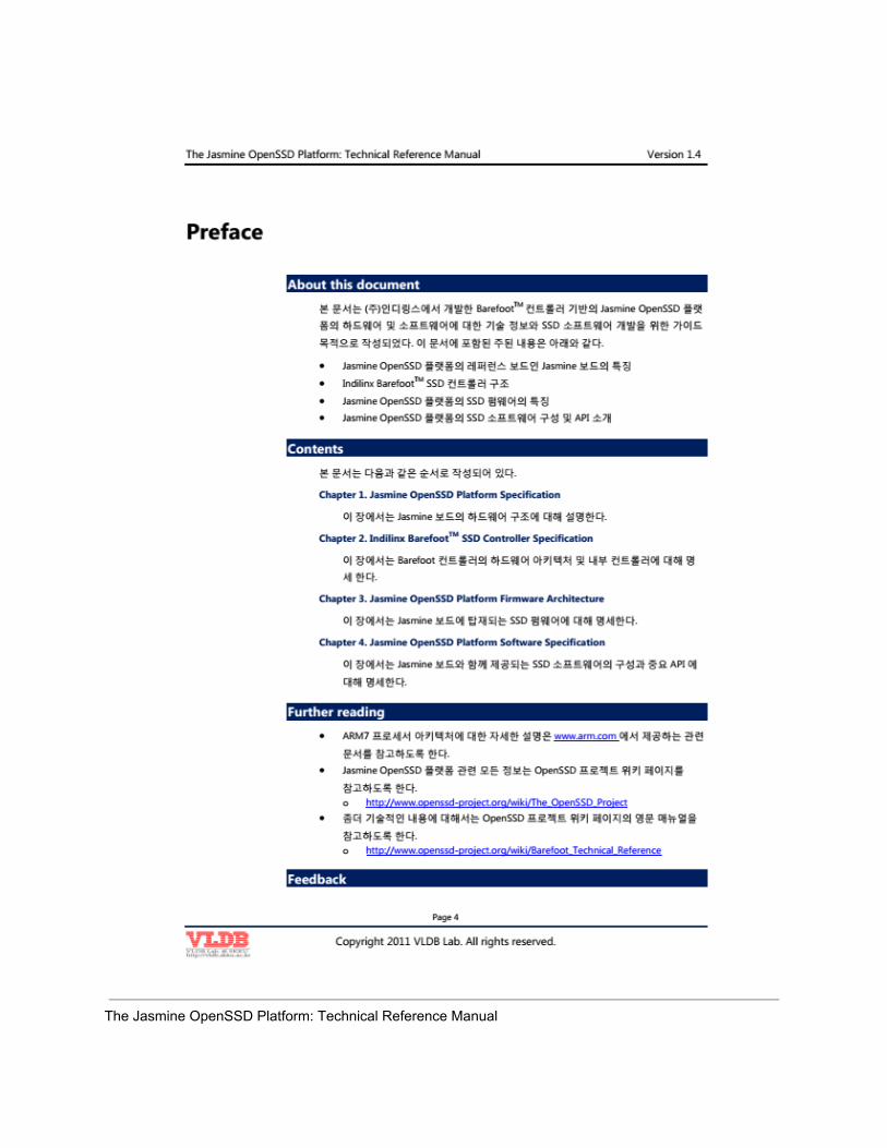
PrefaceAbout this documentThis document is the (main) developed by indie SpringsBarefoot
TM
Jasmine OpenSSDcontrollerbasedplatform
hardware and software for the development of technical information and SSD softwareforguide.
was writtenthe purpose of The main information contained in this document is as follows.
• Jasmine OpenSSD platform features reference board, the Jasmine board
• Indilinx Barefoot
TM
structureSSD controller
firmware • Jasmine OpenSSD Platform FeaturesSSD
• Jasmine OpenSSDSSD software configuration of the platform and API Introduction
Contentsof this document is to be written in the following 1.
order.Chapter Jasmine OpenSSD Platform Specification
JasmineThis chapter describes the hardware structure of the 2.
board.Chapter Indilinx Barefoot
TM
SSD Controller Specification
This chapter describes the hardware architecture of Barefoot controller andinternal controller forpeople.
thethree 3.
Chapter Jasmine OpenSSD Platform Firmware Architecture
In this chapter, the board is mounted on Jasmine specification for the SSD 4.
firmware.Chapter Jasmine OpenSSD Platform Software Specification
This chapter describes the Jasmine SSD software that comes with the board configuration and criticalforAPI.
specifications the
Further reading• ARM7 processor architecture provides a detailed description of the relevantwww.arm.com
documentation forto the.
• Jasmine OpenSSD platform for all information related to the wiki pagethe projectOpenSSD.
forto be o http://www.openssdproject.org/wiki/The_OpenSSD_Project

• For more technical information about the project wiki page OpenSSD English
refer to themanual.o http://www.openssdproject.org/wiki/Barefoot_Technical_Reference
Feedback
The Jasmine Platform: Technical Reference ManualOpenSSD

OpenSSD•project homepage (http://www.openssdproject.org/)
Page 5
Copyright 2011 VLDB Lab. All rights 1.
Version 1.4

Barefoot SSD controller (ARM7TDMIS core)
3Gbps SATA host interface
JTAG debug port
The Jasmine OpenSSD Platform: Technical Reference Manual
reserved.Chapter Jasmine OpenSSD PlatformSpecificationThis chapter details Jasmine OpenSSD platform for the specification of the hardware in 1.1.
OpenSSD Platform overviewJasmine
Jasmineboard
general.OverviewIndie SpringsJasmine OpenSSD highperformance platformBarefoot
TM
equipped withSSD controllerrecord
board conference(Jasmine board) and to support the SATA 2.0 SSD Firmware (Jasmine firmware)
include1.2.
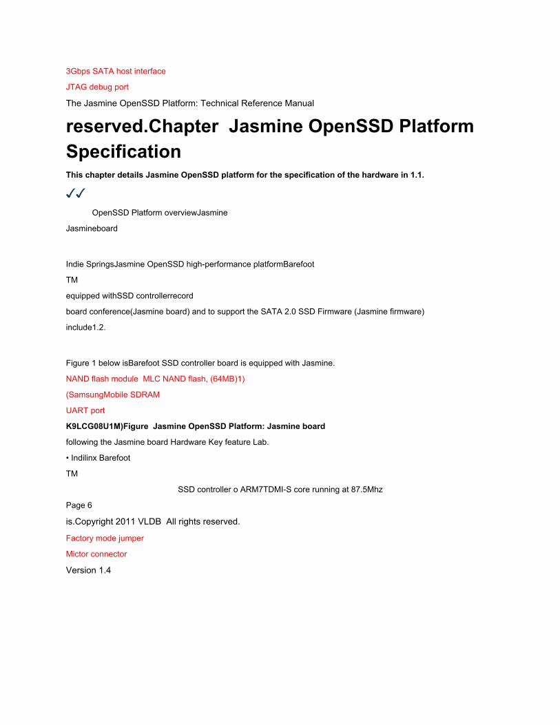
Jasmine BoardFigure 1 below isBarefoot SSD controller board is equipped with Jasmine.
NAND flash module MLC NAND flash, (64MB)1)
(SamsungMobile SDRAM
UART port
K9LCG08U1M)Figure Jasmine OpenSSD Platform: Jasmine board
following the Jasmine board Hardware Key feature Lab.
• Indilinx Barefoot
TM
SSD controller o ARM7TDMIS core running at 87.5Mhz
Page 6
is.Copyright 2011 VLDB All rights reserved.
Factory mode jumper
Mictor connector
Version 1.4
The Jasmine OpenSSD Platform: Technical Reference Manual

o DRAM access bus, flash / SATA control running at 175Mhz o 96KB internal RAM o SATA 2.0 host interface(3Gbps) with NCQ support o Mobile SDRAM controller up to 64MB (running at up to 175MHz) o NAND flash BCH8/12/16 bit correction per sector o SDRAM Reed Solomon 2 byte correction per 128 + 4 byte o NAND flashcontroller up to 64 CE's (4 channels, 16 bits / 8channel)Samsung, Hynix, Toshiba, Micron,
channel,banks / Separate access bus for transferring data between DRAMoNAND flash
oDRAMNAND flashmemory andbufferSupports variousmemory chips from different vendors such as
etc. o Specialized hardware buffer management memory utility functions o Debugging monitoringaidsandforfor/
forand/ JTAG UART 1 LED6 GPIO pins Mictor connector to NAND flash signalslogic analyzer Separate currentmeasurement pointscore, IO,SDRAM, and NAND
Mobile SDRAM 64MB •(DIMM)ofrom Samsung (subject to change)
NAND•ofrom Samsung (subject to change)8flash memory slots 64GB
1.2.1.Indilinx BarefootTM SSD controllerIndiespecification Springs Barefoot SSD controller Chapter 2 of this document sheets.
1.2.2. Factory mode jumperJasmine board with jumper Factory mode, in which the Barefoot controller jumper
pin is connected to GPIO # 0. CPU board when power is suppliedthe ROM address 0 of the address
tospace,so the mapping ROM code is executed begins. ROM code is a simple hardware
initialization after undergoing a process to check the status of GPIO # 0. The pins according to the state ofas
the subsequent operation will be differentfollows.
• GPIO # 0 of the value of zero (if a jumper is in the Normal position)
ROM code is loaded to the location and number of NAND flash caught behind, 0blocks of time
SRAMto read and load the firmware image, address remap operation by the CPU
address space SRAM address 0 is not in the ROM so thatjumpsback to zero
it after.In this way, the firmware is started. If 0, the contents of the block once accidentally
gets erased or damaged due, or any other reason, the block number 04 of the
on pagesignature (0xC0C2E003) is not found, the firmware loading process is
interrupted and enter the Factory mode.
• GPIO # 0 if the value is 1 (Factory mode if the position of the jumper)
ROM code to initialize the SATA interface and waits for commands from the Lab.
Page 7
install.exe.Copyright 2011 VLDB All rights reserved.
Version 1.4
The Jasmine OpenSSD Platform: Technical Reference Manual
Page 8
Copyright 2011 VLDB Lab. All rights 2.
Version 1.4
reserved.Chapter Indilinx BarefootTM SSDController SpecificationOpenSSD Barefootplatform mounted on the indie Springs
TM
ARMbased SATA controller as the controller, the
currentto be mounted on a variety of SSD product family. This chapter describes the hardware architecture ofBarefoot controller
thediscussed. This chapter includes the following topics mainly.
Indilinx Barefoot architecturecontrollercontroller
mapMemory
controllerNAND flash WR (NCQ,queue)&
(FCP,BSP)SATA SATA event
&DRAM host bufferBuffer manager
Memoryutility
Interrupt controller
2.1.Hardware ArchitectureFigure 2 below Jasmine Platformof the H / W architecture is shown inblock
thediagram.
INDILINX BarefootTM ControllerController
Clock Generator
SRAM (96KB)
Controller
NAND Flash
UART
ROM
ARM7TDMIS
GPIO
Core
Timer
WDT
Buffer
PMU Manager
ICU
SATA Host interface DRAMDRAM
APB Bridge
AHB
NAND Controller
SATA Device
DRAMController
Memory Utility
BP
Access Bus
JTAG
JTAGdebug port
Figure 2) Jasmine OpenSSD Platform architecture
Barefoot controller is ARMbased controller as SATAcompatible SSD,many SSD
to be mounted onproduct family.Barefoot controller is ARM, Ltd 16/32bit ARM7TDMIS RISC's
builtin microprocessor. ARM7TDMISS is internallyAMBA bus and
ARMv4Tto be implemented by way of the von Neumann architecture.
A
The Jasmine OpenSSD Platform: Technical Reference Manual
Barefoot controller is basically a 96KB system (SDRAM / NAND manager
SRAM,managercontroller),bufferand SATA 2.0 host interface, clock generator, UART, timer, WDT (Watchdog timer), PMU (Power Management Unit), ICU (Interrupt Control Unit), JTAG, and the like. Barefoot controller, the external component of the SLC / MLC NAND
flash,Mobile DRAM, and the like.
2.1.1. NAND flash architectureBarefoot SSD controller of the NAND Flash architecture is to provide highbandwidth
multichanneland multiway design was based. Each channel is connected to the way NAND
flashmemory chip (s) in the bank by the firmware can perform IO units.
Figure 3 is a NAND Flash architecture platform Jasmine OpenSSD shows.
Way
IO Bus
A0 A1 .. .
A7
"High"
CE
RB
.. 7](0)IO
[0p p (1)
IOBus
8
... p (m)(0)
p
............
Virtual page NAND
sizeflash controller
16
B0 B1
B7 IO .. 15] 8
[8
C0 C1
C7
"Low"
(m1)b b b (2plane mode)3)
D0 D1 ...
D7
(1)(n1)Virtual block size
NAND flash architecture Figure
Figure 3,as shown to the left of the NAND Flash architecture Jasmine platforma fully parallel,
isindependently of the 4 channel is designed to be operated. Each bank has eight channel
exists,and this bank is shown at the right side of Figure 3 connected hardwaretwo
consists ofNAND flash chip. In addition, each bank is 16bit IO bus (Data bus) at the same time via
the input data from the two chips, CE (Chip Enable) input pin and the R / B (Ready / Busy)pins to output
includes a number of controlpin (Control pin ) through a flash controller that the NAND
controlsflash.
NOTE: CE pin is in fact in order to control two separate chips, which is usuallyunison
inenable / disable is (cf only a particular chip enable / disable is possible, which is
Table 1 of the FO_H, FO_L options, please refer
to),while one bank of eight channel IO bus connected because they shareIO operation itself
a number of bank for thecan not be done at the same time. However, NAND flash chips inside cell
Page 9
Copyright 2011 VLDB Lab. All rights Lab.
Version 1.4
The Jasmine OpenSSD Platform: Technical Reference Manual
Page 10
reserved.Copyright 2011 VLDB All rights reserved.
Version 1.4
operation is possible in parallel. However, the hardware design, the flash controllera single
withinchannel bank for one of two R / B output pin at the same time because it hasnonbank 8,
a the maximum of four bank interleaving IO is possible. This means that in the case of channel A, A0 and
A4, and A1/A5, A2/A6, A3/A7 bank is one of the R / B output pin tied. Thus, A0
and A4 bank simultaneously for cell operation is impossible.
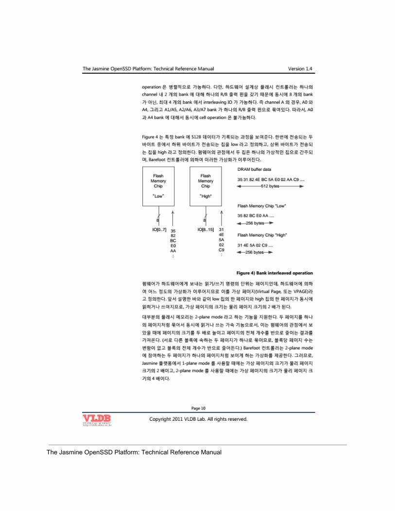
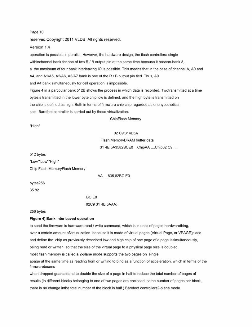
Figure 4 in a particular bank 512B shows the process in which data is recorded. Twotransmitted at a time
bytesis transmitted in the lower byte chip low is defined, and the high byte is transmitted on
the chip is defined as high. Both in terms of firmware chip chip regarded as onehypothetical,
said Barefoot controller is carried out by these virtualization.
ChipFlash Memory
"High"
02 C9:314E5A
Flash MemoryDRAM buffer data
31 4E 5A3582BCE0 ChipAA ....Chip02 C9 ....
512 bytes
"Low""Low""High"
Chip Flash MemoryFlash Memory
AA.... 835 82BC E0
bytes256
35 82
BC E0
02C9 31 4E 5AAA:
256 bytes
Figure 4) Bank interleaved operation
to send the firmware is hardware read / write command, which is in units of pages,hardwarething,
over a certain amount ofvirtualization because it is made of virtual pages (Virtual Page, or VPAGE)place
and define the. chip as previously described low and high chip of one page of a page issimultaneously,
being read or written so that the size of the virtual page to a physical page size is doubled.
most flash memory is called a 2plane mode supports the two pages on single
apage at the same time as reading from or writing to bind as a function of acceleration, which in terms of thefirmwarebeams
when dropped gearsextend to double the size of a page in half to reduce the total number of pages of
results.(in different blocks belonging to one of two pages are enclosed, sothe number of pages per block,
there is no change inthe total number of the block in half.) Barefoot controllers2plane mode

participating in thetwo pages that look like a single page provides virtualization. Therefore,
Jasmine platforms when using the 1plane mode of the virtual page size isthe physical
2 times the size ofpage,2plane mode when using the virtual page sizephysical
is 4 times thepage [0.
8
size.IO 15]
.7]IO [8 ..
The Jasmine OpenSSD Platform: Technical Reference Manual
block erase operation is a read / write because it is the subject of virtualization, like, 1plane mode toused
be when the size of the physical block size of the virtual block 2 times that, 2plane mode is used when the
block size of a virtual physical block size is four times the
otherhand, Jasmine IO platforms in order to maximize the parallelism in basically two bank
enable both NAND flash chip but optionally, flash When you pass a command (FO_L /
FO_H) option is enabled, transferred from the flash controller command / input signal
can be made to ignore the above as Figure 4, for example, FO_H option is enabled, theflash,
command is passed to the the High Low Chip Chip is disabled, only the [35 82 BC ...]data
the is written to the write operation will be simply ignored if the gig, but in the case of a read operation
High values can be read from the chip, so unexpected note
should, butECC / CRC enginespecific chip to selectively perform because they are not, FO_L or FO_H
When the option is enabled, IO performs during "uncorrectable data corruption ˮ interrupt occurs
it is. refer to such an interruption occurs to bypass the flash command option towhen passing
be omittedFO_E.
NOTE: Jasmine on board a more detailed description of the hardware designtheOpenSSD Project
ofJasmine board schematicHOME and the NAND flash module schematic
Flash command (FCP) has been described in this document refer to the section
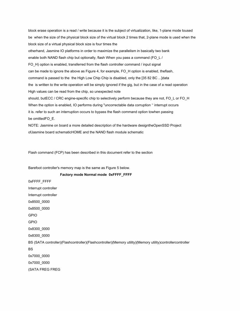
2.3.1. 2.2.Memory MapBarefoot controller's memory map is the same as Figure 5 below.
Factory mode Normal mode 0xFFFF_FFFF
0xFFFF_FFFF
Interrupt controller
Interrupt controller
0x8500_0000
0x8500_0000
GPIO
GPIO
0x8300_0000
0x8300_0000
BS (SATA controller)(Flashcontroller)(Flashcontroller)(Memory utility)(Memory utility)controllercontroller
BS
0x7000_0000
0x7000_0000
(SATA FREG FREG
0x6000_0000
0x6000_0000
MREG
MREG
0x5000_0000
0x5000_0000
controller)DRAMDRAMDRAM DRAM
0x4800_0000
0x4800_0000
0x4000_0000
0x4000_0000
SRAM ROM
0x1000_0000
0x1000_0000
ROM
SRAM
0x0000_0000
0x0000_0000
Figure 5) Memory map
11Page
Copyright 2011 VLDB Lab. All rights reserved.Copyright 2011 VLDB Lab. All rights reserved.
Version 1.4Version 1.4
The Jasmine OpenSSD Platform: Technical Reference Manual
Page12
first, ROM has Booting into Factory mode are stored in the code.
NOTE: Factory mode to install the firmware on the board for Jasmine mode is in this boot
mode,the code stored in ROM are performed, the binary image of the firmware by the user,
firmwareMetainformation for the operation of the flash memory can be installed to defaultof Jasmine
firmware VBLK # 0to record this information, and after the installation of the firmware Jasmine board
poweris applied to theVBLK # 0 is written to the boot loader firmware SRAM image load, since
the firmware operation is performed.
this mode, the ROM is mapped at address 0x0000_0000, install a firmwarestoredin ROM
code is being performed, Normal (Nonfactory) mode, the ROM memory addresses SRAM
memory address and other changes (remap) to.
SRAM has been mapped at address 0x1000_0000 in Factory mode code is loaded into ROM,
Normal mode and the main firmware image, the boot loader and firmware ZI / RO / RW data
is loaded teodeulother
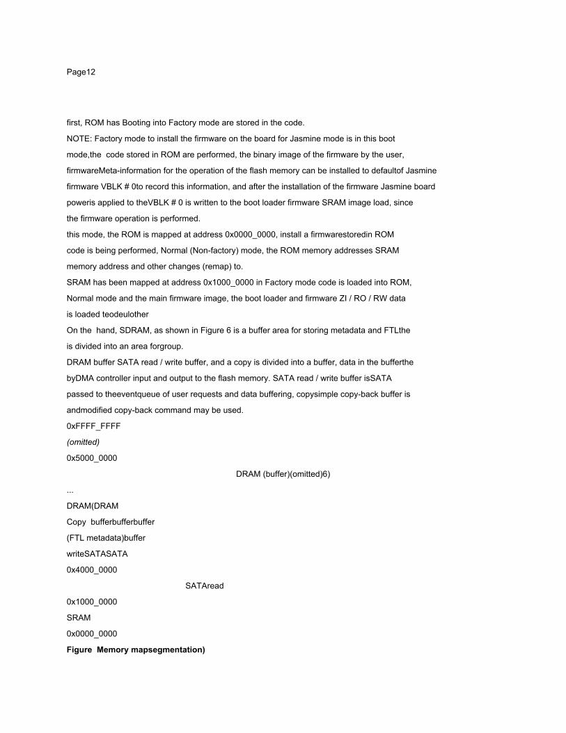
On the hand, SDRAM, as shown in Figure 6 is a buffer area for storing metadata and FTLthe
is divided into an area forgroup.
DRAM buffer SATA read / write buffer, and a copy is divided into a buffer, data in the bufferthe
byDMA controller input and output to the flash memory. SATA read / write buffer isSATA
passed to theeventqueue of user requests and data buffering, copysimple copyback buffer is
andmodified copyback command may be used.
0xFFFF_FFFF
(omitted)
0x5000_0000
DRAM (buffer)(omitted)6)
...
DRAM(DRAM
Copy bufferbufferbuffer
(FTL metadata)buffer
writeSATASATA
0x4000_0000
SATAread
0x1000_0000
SRAM
0x0000_0000
Figure Memory mapsegmentation)

Read
NAND flash that contains the user data read from the buffer.the requestedthe host
Read all ofdata tois placing the buffer, SATA controller, passing the host
The Jasmine OpenSSD Platform: Technical Reference Manual
it is this only the user data stored in the buffer. mapping tableinternal including firmware
to read thedata,out the buffer space when not used.
SATA Write buffer
FTL allows a host is passed to the user in order to write data to the NAND Flash,controller,
SATA the buffer is put user data.
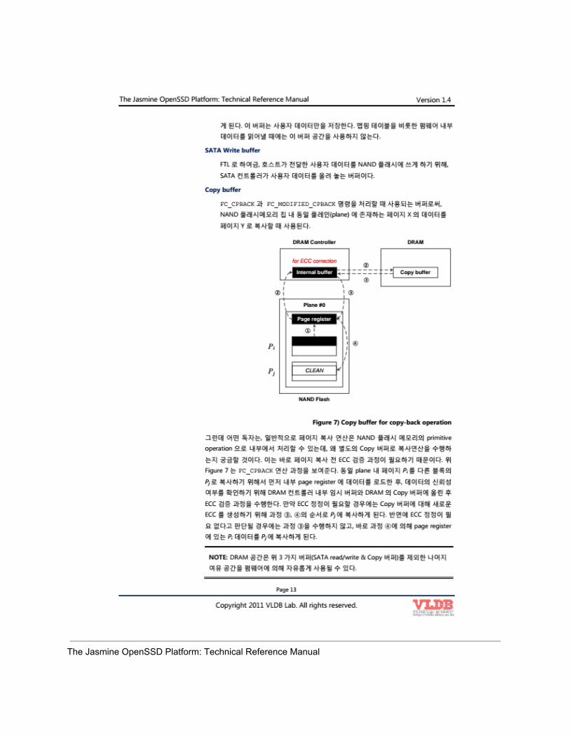
Copy buffer
FC_CPBACK to process commands and FC_MODIFIED_CPBACK As the buffer used,
NAND flash memory chips in the same plane (plane) onin a page of data X
the pageto Y is used when copying.
Controller DRAM
DRAM
for ECC correction
Internal buffer Copy buffer2
33
2
Plane # 0
Page register
1
PPi
4
j
CLEAN
NAND Flash
Figure 7) Copy buffer for copyback
operation,but some readers are, in general, NAND flash memory, page copy operationsprimitive
that can be processed by the underlyingoperation, why separate Copy bufferwonder,do the copy operation
may will copy this page just before ECC verification process is necessary.in
FC_CPBACK operationsthe process of Figure 7 shows the same plane on my page P i
Page 13
Copyright 2011 VLDB Lab. All rights reserved.
to another block
P j
is copiedin order to load data into the first internal page register, and thenthe reliability of the data
to determine whetherinside the temporary buffer DRAM controller and DRAMAfter posting the Copy buffer
ECCto perform the verification process . If ECC correction is needed if the Copy Bufferfor the new
for generating ECCprocess 3, 4, P j in order
to make copies, while the ECC correction isnecessary
determined to be not if the process is not performed 3 but, justthe process page register by 4
inP i
P jdata from
to copy thethe.
NOTE: DRAM buffer space in three kinds (SATA read / write & Copy buffer) except
firmware free by free space can be Lab.reserved.
Version 1.4Version 1.4

The Jasmine OpenSSD Platform: Technical Reference Manual
Page 14
used.Copyright 2011 VLDB All rights
continues, 0x4800_0000 dong the DRAM and memory controller registers are mapped,
0x5000_0000 From memory, the utility registers threedong ( MREG) for allocated.
register value is set in this area becomes the DMA is operating.
NOTE: Barefoot hardware memory controller is equipped with a utility by DMA
between the DRAM and SRAM memory copy and H / W engines utilizing such as a navigationfaster
support formemory.
SATA controller register set (BS) and is mapped at address 0x7000_0000, 0x8300_0000a
From GPIO pins are mapped tobungee.
interrupt register set is mapped at address 0x8400_0000 and interrupt controller to the group
seen as SATA / Flash / DRAM controller and APB (Advanced Peripheral Bus) connected to
componentarethe interrupt request is processed.
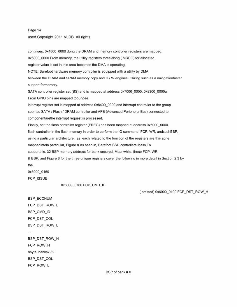
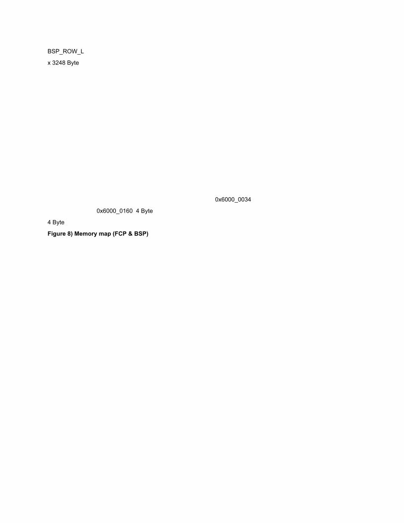
Finally, set the flash controller register (FREG) has been mapped at address 0x6000_0000.
flash controller in the flash memory in order to perform the IO command, FCP, WR, andsuchBSP,
using a particular architecture, as each related to the function of the registers are this zone,
mappedintoin particular, Figure 8 As seen in, Barefoot SSD controllers Mass To
supportthis, 32 BSP memory address for bank secured. Meanwhile, these FCP, WR
& BSP, and Figure 8 for the three unique registers cover the following in more detail in Section 2.3 by
the.
0x6000_0160
FCP_ISSUE
0x6000_0760 FCP_CMD_ID
( omitted) 0x6000_0190 FCP_DST_ROW_H
BSP_ECCNUM
FCP_DST_ROW_L
BSP_CMD_ID
FCP_DST_COL
BSP_DST_ROW_L
...
BSP_DST_ROW_H
FCP_ROW_H
8byte banksx 32
BSP_DST_COL
FCP_ROW_L
BSP of bank # 0
BSP_ROW_L
x 3248 Byte
0x6000_0034
0x6000_0160 4 Byte
4 Byte
Figure 8) Memory map (FCP & BSP)
The Jasmine OpenSSD Platform: Technical Reference Manual
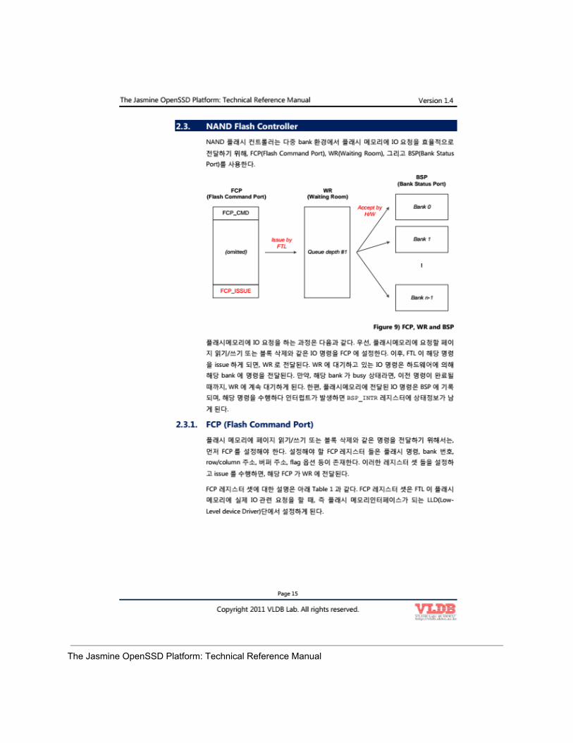
2.3. Flash Controller NANDNANDflash controller is a multibank flash memory, IO request environmentefficient,
to deliver FCP (Flash Command Port), WR (Waiting Room), and BSP (Bank Status
Port) is Lab.reserved.
Issue by FTL
Page 15
used.Copyright 2011 VLDB All rights
BSP Status FCP(FlashPort)
(BankPort)WR Command
(Waiting (omitted)9)
Accept by H / W
Queue depth # 1
Room)Figure FCP, WR and BSP
IO requests to the flash memory in the process is as follows: First, a flash memory, a request to
pagea read / write or block IO commands, such as deleting the FCP set. later, FTLthe correct
When issuecommand,WR delivered to. WR IO command in the atmosphere by the hardware
that passes commands to the bank if, the bank the busy state, completion of the previous
until thecommand,WR continues to wait, while IO command is passed to the flash memory written to
areBSP,the command to be performed when an interrupt occurs, status information is the register BSP_INTRman.
it is
2.3.1.FCP (Flash Command Port)flash memory page read / write or block erase command to the same order,
first, to set the FCP must be set in the flash command register FCP, bank number ,
row / column address buffer address, flag options exist, such as these three registers are set
to perform at the issue, the FCP is passed to WR.
FCP for a description of the three registers shown in Table 1 below. FCP This register sets the FTL flash
memory when the actual IO related requests, ie the flash memory interface, LLD
(LowLeveldevice Driver) to set the stage.
0 FCP_CMD BankBank
Bank1n1
FCP_ISSUE
Version 1.4
The Jasmine OpenSSD Platform: Technical Reference Manual
Page 16
Copyright 2011 VLDB Lab. All rights reserved.
Version 1.4
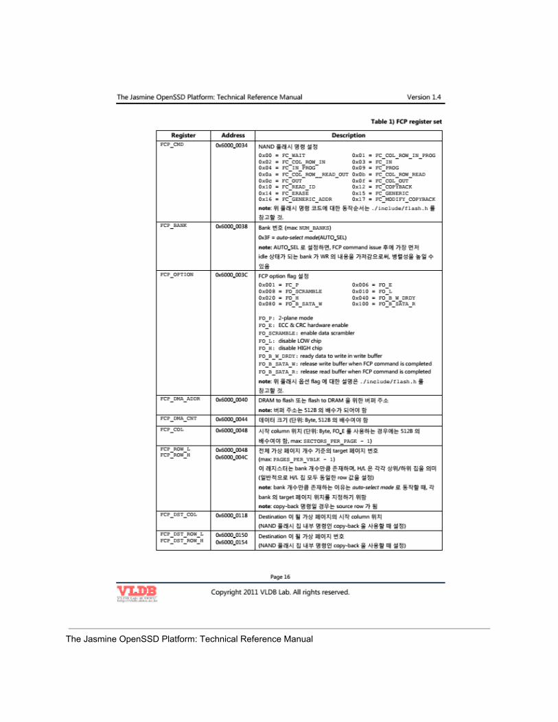
Table 1) FCP register set
Register Address Description FCP_CMD
0x6000_0034
NAND Flash command set to 0x00 = FC_WAIT 0x02 = FC_COL_ROW_IN 0x04 = FC_IN_PROG 0x0a =FC_COL_ROW__READ_OUT 0x0c = FC_OUT 0x10 FC_READ_ID 0x14 = FC_ERASE 0x16 =FC_GENERIC_ADDR========
=0x01FC_COL_ROW_IN_PROG 0x03FC_IN 0x09FC_PROG 0x0bFC_COL_ROW_READ 0x0fFC_COL_OUT0x12FC_COPYBACK 0x15FC_GENERIC 0x17FC_MODIFY_COPYBACK note: in order for a motion command code
flash. / include / flash.h to
consult it. FCP_BANK
0x6000_0038 Bank number note:
NUM_BANKS)0x3F = autoselect mode(AUTO_SEL)AUTO_SEL
(max:is set to, FCP command issueafter the first
the bankidle state by going to import the contents of the WR, parallelism increase
canFCP_OPTION
0x6000_003C
FCP option flag setting 0x001 FC_P 0x008 = 0x020 = FO_H 0x080 = FO_B_SATA_W====FO_SCRAMBLE:
=0x006 0x010FO_L 0x040FO_B_W_DRDY 0x100FO_B_SATA_RFO_E:
FO_SCRAMBLEFO_EFO_P: 2plane mode ECC & CRC hardware enable enable data scrambler disable LOWchip FO_H: disable HIGH chip FO_B_W_DRDY: ready data to write in write buffer FO_B_SATA_W: release writebuffer when FCP command is completed FO_B_SATA_R: release read buffer when FCP command is completed
FO_L:note:in the description for the flash option flag the. / include / flash.h to
consult it. FCP_DMA_ADDR
0x6000_0040
DRAM to flash or flash to DRAM buffer address for the
note: buffer address must be a multiple of the 512B FCP_DMA_CNT
0x6000_0044
data size (unit: Byte, 512B must be a multiple ofFCP_COL
column0x6000_0048 start position (Unit: Byte, FO_E If you useof
must be a multiple512B,max: SECTORS_PER_PAGE 1) FCP_ROW_LFCP_ROW_H
0x6000_0048
total number of pages based on the virtual page number of the target 0x6000_004C
(max: PAGES_PER_VBLK 1) in this register exist as a bank number, H / L are each upper / lower means that thechip
(typically a H / L value is set row all have the same chip)
note: bank number as the reason for the autoselect mode when operating, Each
bank intended to specify the location of the target page
note: copyback command when the source row is FCP_DST_COLHas
0x6000_0118
Destinationto be the starting column location of the virtual page
(NAND flash chip when you use the command set of copyback)FCP_DST_ROW_LFCP_DST_ROW_H
0x6000_0150 0x6000_0154
beDestination virtual page number
(NAND flash chip when you use the command set of copyback)
The Jasmine OpenSSD Platform: Technical Reference Manual
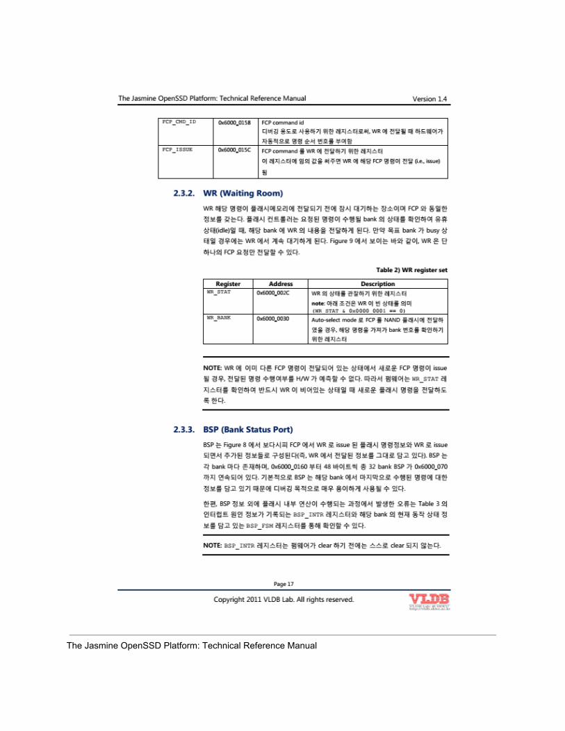
FCP_CMD_ID
0x6000_0158 FCP command id
used for debugging purposes as a register, WR will be passedthe hardware will
command,automatically be given a sequence numberFCP_ISSUE
to WR0x6000_015C FCP command register for forwarding
write any value to this register that give FCP commands are passed to WR (ie, issue)
Has
2.3.2. WR (Waiting Room)WR, the command is passed to the flash memory, and a place to pause before FCPthe sameas
hasinformationthe flash controller performs the requested command to check the status of the bank to be
idle(idle), when, on its bank to pass the contents of the WR, if the target bank is busyphase
if the WRTaeil continue to wait. Figure 9, as shown in, a
WR,onlysinglepass of the FCP may be requested.
Table 2) WR register set
Register Address Description WR_STAT
0x6000_002C
WR for observing the state of the registers
note: The following conditions are to be empty meaning WR (WR_STAT & 0x0000_0001 == 0) WR_BANK
0x6000_0030
Autoselect mode to FCP anddelivered to the NAND
wasflash,the command Take thebank number identifying
registerfor
NOTE: WR command is transmitted to the FCP is already in a state different from the new issuethe FCP
whencommand,whether to perform the command passed H / W is not predictable, so firmware willWR_STATregister
Be sure to check the is empty when the WR command to the new flashprimer.
lock the
2.3.3. (Bank Status Port) BSPBSPAs you can see in Figure 8 in FCP is to issue a Flash command information and WR WR to issue
consists of the additional information (ie, WR still contains the information passed). BSP is
present in each and every bank, 0x6000_0160 from 48 bytesa total of 32 bank BSP is 0x6000_070
up toto be continuous. default BSP is performed corresponding to the last bankon the command
contains informationfor debugging purposes because it can be used very
easily, while,BSP internal flash operations are performed in addition to information on the error that occurred in theprocess of Table 3 are
more interrupt sources recorded in the register and that BSP_INTR bankthe current operating status
informationwhich containscan be confirmed by BSP_FSM register.

NOTE: BSP_INTR register yourself clear before the firmware is not Lab.reserved.
Page 17
clear.Copyright 2011 VLDB All rights
Version 1.4

The Jasmine OpenSSD Platform: Technical Reference Manual
Page 18
Copyright 2011 VLDB Lab. All rights reserved.
Version 1.4
Table 3) & BSP_FSM registerBSP_INTR
BSP_INTRRegister Address Description
0x6000_0760: 0x6000_0780
Bank interrupt information. (1Byte)
Bank exists separately for each 0x01 = FIRQ_CORRECTED 0x02 = FIRQ_CRC_FAIL 0x04 = FIRQ_MISMATCH0x08 = FIRQ_BADBLK_L 0x10 = FIRQ_BADBLK_H 0x20 = FIRQ_ALL_FF 0x80 = FIRQ_ECC_FAIL 0x82 =FIRQ_DATA_CORRUPT BSP_FSM
0x6000_0780: 0x6000_0800
Bank FSM (Finite State Machine) information. (1Byte)
BSP_INTR register separately for each bank presence, like 0x0 = idle others = no idle
2.4. SATA ControllerBarefoot controller internal data transfers between a host and a device that is responsible for SATA
controlleris present. SATA controllers NCQ (Native Command Queuing) and a separate command queue
(event queue) to efficiently manage the FTL allows the IO to deliver.
NOTE: SATA Operation more technical information on the English menu OpenSSDcommunity
manual forPlease refer to
2.4.1.SATA protocolhost IO request is sent to the SSD, SATA protocol, the command is received bythe automatic
the host in response totransmission. If a write command, the firmware started tothe data
requesttransfer,the transfer is completed for this command until all the process isautomaticallyby the hardware,
handled while
an exceptional condition occurs during performing IO, unless the command for the final response
Hardwarewill be automatically transferred.
2.4.2. SATA NCQSATA NCQdrives at the same time in one of several commands in a row, we can take
for the SATA command protocol.
Barefoot controller, SATA 2.0 NCQ is in accordance with 32 hosts to be able to accept the command
of said FIFO method designed to operate. On the other hand are still SATA NCQ commands are passed todata
the transfer commands are not made. That is, the host perspective,have not yet completedcommands
theyNCQ that are queued. These commands are then moved to the SATA FTLevent
is transmitted to thequeue.
2.4.3. event queueSATA

The Jasmine OpenSSD Platform: Technical Reference Manual
SATAhost the event queue in terms of those already queuing SATA data transfer is completed, andcommand
therole. This command does not perform the actual IO DRAM NAND flash in the
state of waiting for the time of transmission.
Below as Figure 10 up to 128 SATA event queue accepts commands, SATA NCQ andSimilarly
FIFO manner. By the host command is passed to the FIQ interrupt, FTL is
removed each time to take the command.
SATA event queueSATAevent queue
Host
tail
128 NCQ
cmdcmd
32
head
FTL
...
NCQFigure 10)&
Meanwhile, SATA event queue If the FIFO scheme of treatmentsome problems as
can causefollows:1.
Read command can take a long time to be waiting for the host
2.Read data during transmission to the host DRAM progresses, FTL and the NAND flashbeen
memory hasidle (idle) state, there is a high possibility that a disadvantage in terms of performance may be
to solve this problem is a read command, an event queue SATA Writing instructionmore
was designed to handlepreferential.However, this method is for a specific address "readafterwrite ˮfor operations
the data coherencebecause of the potential for problems (for example, <WRITE,
lsn=3> SATA commands are accumulated while the event queue <READ , lsn = 3>the command isfirst
WhenprocessedFTL,old data is taken out from NAND), and due to the hardware history log search
through these data coherence is ensured. Furthermore,sector is in the case of overlappingfor
thethe hardware to solve2.5.
Host Buffer & Buffer Manager DRAMDRAMbuffer is a SATA host IO request to the event queue for buffering the real user datathe
used forgroup, which is requested by the host, read data is passed from the flash memory
for buffering SATA read buffer and SATA write data to the write buffer for buffering
Page 19
Copyright 2011 VLDB Lab. All rights Lab.
Version 1.4
The Jasmine OpenSSD Platform: Technical Reference Manual
Page 20
reserved.Copyright 2011 VLDB All rights reserved.
Version 1.4
is divided into management. This buffer is basically a circular buffer (circular buffer)in the form of
andOperation,DRAM buffer and SATA host controller hardware flow control isbythe buffer
achieved manager.
2.5.1. buffer SATA read / writeSATA read / writebuffer size of the default buffer frames are VPAGE (eg, 4 ~ 32KB) is.eachbuffer
The size ofDRAM space size depends on the metadata within the FTL, which typically SATA read
buffertheabout 1MB, and dozens of SATA write buffer use the MB degree.
NOTE: DRAM size of the host buffer space FTL metadata determined by, FTL header
file (ftl.h) to be written
belowthe SATA read / write register is associated with a buffer.
Table 4) register for read / write SATA buffer
Register Address Description SATA_BUF_PAGE_SIZE
SATAbuffer0x7000_00B4frame size (default size = BYTES_PER_PAGE)SATA_WBUF_BASE SATA_RBUF_BASE
0x7000_0170: 0x7000_0174
SATA write / read buffer's base address
SATA_WBUF_SIZE SATA_RBUF_SIZE
0x7000_0178 0x7000_017C
SATA write / read buffer frame number
SATA_RESET_WBUF_PTR SATA_RESET_RBUF_PTR
0x7000_0184 0x7000_0188
SATA write / read buffer framepointreset register
buffer managementdirectly to the firmware,beused to
can SATA_WBUF_PTR SATA_RBUF_PTR
0x7000_0194 0x7000_0198
SATA write / read buffer pointer (id #)
SATA_WBUF_FREE
0x7000_019C SATA write buffer number of free buffer frame SATA_RBUF_PENDING
0x7000_01A0
SATA read bufferthe number of pending buffer
whileframe,SATA read / write buffer, the actual management of By default, SATA, Buffer Manager,
NAND controller is made between the signal increases, for delivery, if you wantdirectly to the firmware
to engage with themcan be adjusted.
SATA read / write buffer management are described in chapter 2.5.2, the I hope.

2.5.2. Buffer managementDRAM host buffer SATA, hardware buffer manager, and between FTL pointer
(ie, sata_xxx_ptr, bm_xxx_limit,ftl_xxx_ptr) managed by the adjustment. On the other hand,inprevious
as described thesection, DRAM operates in the host buffer is a circular buffer, because each buffer
framepointer is always to be managed to grow high.
Figure 11 is the host buffer DRAM picture of the representation of management policy.
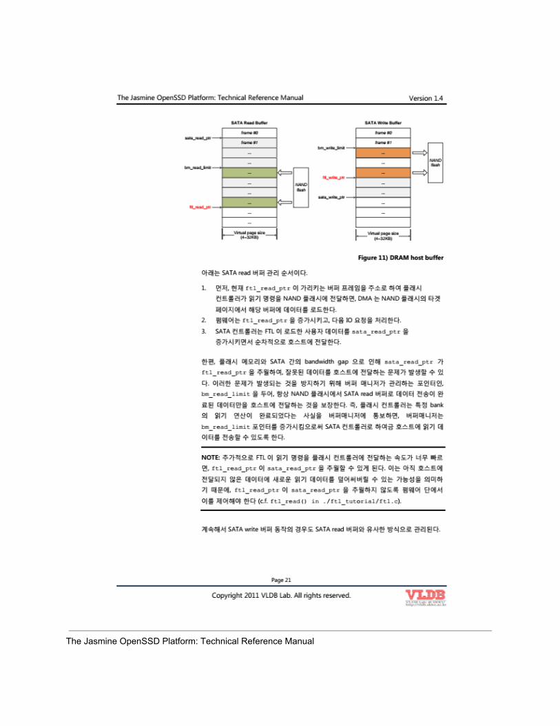
The Jasmine OpenSSD Platform: Technical Reference Manual

SATA Read Buffer SATA Write Buffer
frame # 0frame #frame #
0sata_read_ptr
frame #11
............
bm_read_limit
......
sata_write_ptr
...
Virtual page size (4 ~ 32KB)
Page21
Copyright 2011 VLDB Lab. All rights reserved.
Bm_write_limit
ftl_read_ptr
NANDflash
ftl_write_ptr ...
NAND
......
flash
...............
Virtual page size (4 ~ 11)
32KB)Figure DRAM host buffer
under is managed by the SATA read buffer
1.First, the current frame to address ftl_read_ptr the buffer pointed to byflash
the read command to the NANDcontroller is passed to the flash, DMA is the target of a NAND flash
page to load the data from the buffer to
0.2.Ftl_read_ptr firmware is increasing, the next IO request.
3. FTL SATA controller is loaded by the user dataincreasingsata_read_ptr
while host sequentially transmits the
otherhand, the bandwidth gap between a flash memory and a SATA sata_read_ptr duethe
to overtakeftl_read_ptr, invalid data is passed to the host may be a problem be
it. To prevent such a problem occurs, that is managed by the buffer manager pointer,
bm_read_limit to put it always in the NAND flash SATA read bufferthe data transfer is
only data thatcomplete,ensures that the host is passed. In other words, the flash controllerthea particular bank
has completedread operation ofhas been informed that the buffer manager, the buffer manager
bm_read_limit by increasing the pointer to the SATA controller enables the host to readdata
the to transmit.
NOTE: In addition, the read FTL passing the command to the flash controllervelocity is too
facefast,ftl_read_ptr sata_read_ptr overtake this can be achieved. This hostyet
is not passedread the new data to overwrite the data, means the possibility to use
up,so, ftl_read_ptr sata_read_ptr overtake this stage,to preventfirmware
it should be controlledthe(cf ftl_read () in. / Ftl_tutorial / ftl . c).
continue to SATA write operations, if the buffer is managed in a similar manner to SATA read the Lab.
Version 1.4
The Jasmine OpenSSD Platform: Technical Reference Manual
Page 22
buffer.Copyright 2011 VLDB All rights 1.
Version 1.4
reserved. SATA controllers sata_write_ptr event queue while increasing the queuedto
write requestthe host data buffer to be passed to SATA write, DMAthe NAND
data toFlash to deliver
2.FTL is a request to bring the event queue a command the controllerflash,
toand ftl_write_ptr increases
0.3.SATA controller, to write the data that is passed to the SATA write buffer is completed, the buffer
manager to notify the buffer manager of a NAND flash in the flash controller
to allow the host to write
data, butflash memory is relatively slow Programming speed (tPROG), due to realize NAND
FlashSATA user data were not recorded in a request for anotherwith new data
overwrittencan be discarded. Therefore, to solve these problems even SATA write bufferhardware
managed by the buffer manager bm_write_limit put pointer, sata_write_ptra
bm_write_limit overtakehost write operation by preventing a phenomenon in which the normal operation
guarantee.
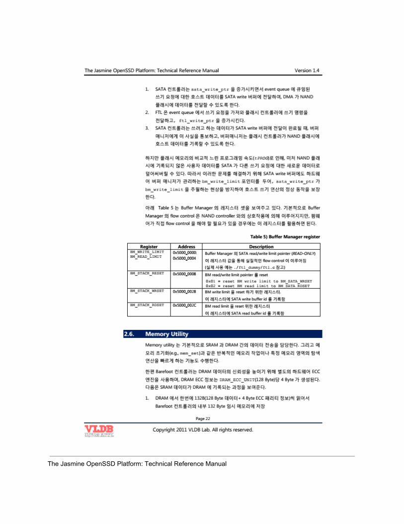
Following Table 5 the Buffer Manager shows a set of registers. Bufferdefault
Manager of the flow controlis made by the interaction with the NAND controller, butfirmware
directly eogaflow control when there is a need to have you to take advantage of this register.
Table 5) Buffer Manager register
Register Address Description BM_WRITE_LIMIT BM_READ_LIMIT
0x5000_0000 : 0x5000_0004
Buffer Manager of the SATA read / write limit pointer (READONLY)
value of this register is the actual flow control yirueojim
(a reallife example. / ftl_dummy / ftl.c Note) BM_STACK_RESET
0x5000_0008
BM read / write limit pointer to the reset 0x01 = reset to BM_SATA_WRSET 0x02 = reset BM read limit toBM_SATA_RDSET BM_STACK_WRSETBM write limit
0x5000_0028
BM write limitto register for reset
thisregister to SATA write buffer id bn BM_STACK_RDSET
0x5000_002C
BM read limit to reseta register
SATA readin the register buffer id andbn.
2.6 Utility MemoryMemoryutility is basically responsible for the transfer of data between the SRAM and the DRAM. Andthe
initializememory(eg, mem_set) memory tasks, such as repetitive or specific memory areasearch
is the ability to quicklyoperations carried out
whilethe DRAM Barefoot controller to increase the reliability of the dataa separate hardware ECC
usingengine and DRAM ECC information is DRAM_ECC_UNIT (128 Byte) per 4 Byte is generated by
followingthe SRAM data are written to the DRAM shows the process:
1.At a time in DRAM 132B (128 Byte data + 4 Byte ECC parity information) by reading the
Barefoot controller's internal temporary memory 132 Byte

The Jasmine OpenSSD Platform: Technical Reference Manual
2. Step 1 of the ECC correction is required, the temporary memory of the data correction
target,performoperation (cf in effect a high reliability memory DRAM ECC correction operation, becauseprobability
the is very low)
3. SRAM read the data you want to modify the contents of the temporary memory
4. New ECC for the new 128 Byte parity is generated and to the DRAM total of 132 Byte
written
NOTE: CPU changes to the DRAM, the data directly to the ECC informationdue to memory
is lostutility,or because you can become meaningless, SRAM and DRAM between the transfer the data
Besure tomemory utility (. / include / mem_util.h) shall be made by the use of.
Memory utilityrelated registers and set the same as Table 6 below, memory utilityona course of action
generates an interrupt of the SDRAM controller registers SDRAM_INTSTATUS checkbylooking at
can be determined the causes.
Table 6) Memory utility register set
Register Address Description MU_SRC_ADDR
0x5000_0010 be copied (source) memory address. Set DRAMwhen reading data
MU_DST_ADDR
0x5000_0014
to be copied (destination) memory address. DRAM write datatothesetMU_VALUE
0x5000_0018
be written tonew dataMU_SIZE
0x5000_001C
setting or the size of the memory area to navigate
note:
mem_search case, max 32768 Bytearea
MU_RESULT
memory0x5000_0020 result value
of 0xFFFFFFFF = mean current MU_CMDperform memory operations
0x5000_0024
Memory utility command codeMU_UNITSTEP
memory0x5000_0030 repetitive work, step Unit
note:
SETREG (MU_UNITSTEP, MU_UNIT_8 | SETREG (MU_UNITSTEP, MU_UNIT_16 | 2); SETREG (MU_UNITSTEP,MU_UNIT_32 | 4);7)
1);Table SDRAM controller register set
Register Address Description SDRAM_INTSTATUS
0x4800_001C
DRAM controller interrupt status caused 0x01 = ECC fail 0x02 = ECC correction 0x04 = Address Overflow 0x08 =
Deadlock
2.7.Interrupt ControllerPeripheralinterrupt controller of the internal SATA, flash memory, DRAM, UART, Timer,
WDT interrupt by the external peripheral device receives the processing request, CPU causes to
eachhandle interrupts from the peripherals to be encountered.
Page 23
Copyright 2011 VLDB Lab. All rights Lab.
Version 1.4
The Jasmine OpenSSD Platform: Technical Reference Manual

Page 24
reserved.Copyright 2011 VLDB All rights reserved.
Version 1.4
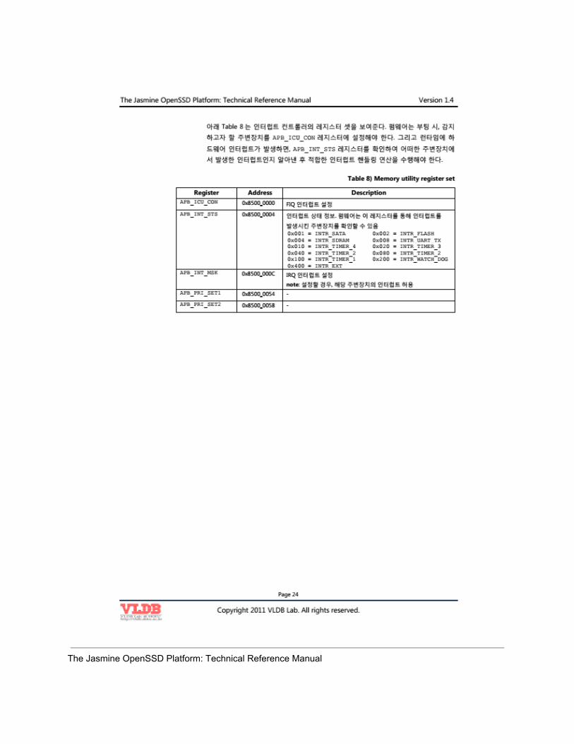
Table 8 below shows the three registers of the interrupt controller. Firmware at boot time,detect
you want toperipherals APB_ICU_CON register must be set. And at
hardwareinterrupt occursruntime,APB_INT_STS check the register any peripheral device
onfigured out what caused the interrupt interrupt handling operations should be suitable.
Table 8) Memory utility register set
Register Address Description APB_ICU_CON
0x8500_0000
FIQ interrupt settings APB_INT_STS
0x8500_0004 interrupt status. Interrupt the firmware thatthis register
causedcan be determined by peripheral 0x001 = INTR_SATA 0x002 = INTR_FLASH 0x004 = INTR_SDRAM 0x008= INTR_UART_TX 0x010 = INTR_TIMER_4 0x020 = INTR_TIMER_3 0x040 = INTR_TIMER_2 0x080 =INTR_TIMER_2 0x100 = INTR_TIMER_1 0x200 = INTR_WATCH_DOG 0x400 = INTR_EXT APB_INT_MSK
0x8500_000C IRQ interrupt setting
note: If set, the peripheral allows the interrupt APB_PRI_SET1
0x8500_0054
APB_PRI_SET2
0x8500_0058
The Jasmine OpenSSD Platform: Technical Reference Manual

Chapter 3.Jasmine OpenSSD Platform FirmwareArchitectureThis chapter describes theJasmine OpenSSD platform for the specification of the internal structure of the SSDfirmware to
3.1.Firmware OverviewFirmwareJasmine OpenSSD main platform is largely HIL FTL Layer),(Flash Interface Layer)
(Host Interface Layer),(FlashTranslationFILto be structured.
HIL SATA host command is primarily responsible for managing the buffer layer and by the hostfrom the SATA
IO request is passedcontroller, the corresponding command is inserted into the event queue SATA FTL since this
helps to handle the request
sequence,followed by FTL flash memory as a block device, such as a hard disk so that you can recognize
the software layer. FTL is usually 1) address mapping function, 2) garbage collection, and 3)hemp,
the equalization function and the charge mode, and IO request processing is the entity FTL in the flash memory,the operation
takes place by passing. FTL is a variety of techniques to increase the performance and reliabilitywill
whichexist,Jasmine firmware includes Tutorial FTL, Greedy FTL, and Dummy FTL is
implemented.
FIL layer is responsible for the flash memory, FTL flash command passed from the actual behavior of the
LLD (Lowlevel device driver) carried out by, an exception occurs during normal operation block,
(eg,runtime bad data corruption) are then detected by the interrupt controller, FTL ishandle.
bundling the
3.2. Host Interface Layer
3.2.1. Hardware event queueJasmine firmware for the SATA event queue (see section 2.4.3) is to be implemented in hardware,event
thequeue.SATA interface is passed to read / write ATA command isby a hardware event
being managedqueue,HIL (Host Interface Layer) FTL is transmitted to the main function of treatment. Below is the
ATA command is processed by the event queue shows the process:
1.Jasmine ATA commands from the host to passboards.
two SATA host interface and FIQ FIQ interrupt handler called generation
3. FIS (Frame Information Structure) read from the command. Request command
cmd_type, lba,sector_count extract
4. Read / write operations (CCL_FTL_D2H/CCL_FTL_H2D), the hardware event queue,the
addcommand (. / Sata / sata_isr.c the handle_got_cfis ())
5. Read / write other commands (eg TRIM such as slow command) if,
g_sata_context.slow_cmd variable storage

Page 25
Copyright 2011 VLDB Lab. All rights Lab.
Version 1.4
The Jasmine OpenSSD Platform: Technical Reference Manual
Page 26
reserved.Copyright 2011 VLDB All rights 6.
Version 1.4
reserved. The main function firmware (. / Sata / sata_main.c the Main ())processing the command
o Event queueread / write request, one priority to take out
(. / Sata / sata_main.c the eventq_get ())
o If the read / write request in the absence of, slow_cmdCommand processing is stored in a
3.3variable.Flash Translation Layer(FlashTranslationFTL Layer)is host to flash memory that you can look like a hard disk
sois a software layer. FTL is embedded in a hardware event queue read / write requests to
obtainand subsequently processed, and the command to the IO controller in flash.
3.3.1. protocol interface FTLFTLprotocol interface for SATA host interface and functions for sending and receiving messages
mean. In this section, four key protocol interface ftl_read /
(ftl_open,ftl_write,ftl_flush) function that must be implemented for any functionmainly in
to be describedwhether.
NOTE: FTL protocol API specification of the function See Section 4.2 of this document
ftl_open
Jasminethe function of the board after completing the initialization process, the host IO request to acceptof
the FTLthe functions that must be performed to initialize:
1.Firmware install time, recorded in written VBLK # 0 scan listyou read the initial bad block
to make sure2.
NAND flash memory to the host IO request processing to the initial state.user
For writing data to the deleting the entire block (format) that the operation may
be included.
3. Installing the firmware installed on the flash memory before FTL metadata or
poweroffmetadata information is recorded at the time of the SRAM or DRAM to load
4.FTL including volatile variables managed by the metadata information and initializes the other
5.The flash controller, and sets the interrupt option.
Ftl_read
Event queue read request transmitted from the host for processing the API. Mappingmapping
theinformation, virtual page units of valid pages in the flash memory chips belonging to a read
commandpasses. SATA read and FTL managed to adjust the buffer pointer.
Ftl_write
Event queue write requests sent from the host to the API.dataa new
Space for writing topage (free pace) to write data to a new location, lookingthe existing

evermapping information to change the information on the new page.
Ftl_flush
The Jasmine OpenSSD Platform: Technical Reference Manual
POR / SPOR must be preserved for metadata information to FTL NAND flash
memoryis written to the API. This API supports the SATA idle / standby when called periodicallyis
FTL metadata consistency and PORpossible.
3.3.2. Tutorial FTLTutorial FTLFTL on the platform architecture Jasmine easily understand the operating principleShiki
has been implemented for the purpose ofgroup. FTL history of the page addresses based on this technique isused, and,
FTL,a key feature of garbage collection / wearleveling / POR, and the like are nota very simple
to be implemented instructure.In this section, we take advantage of DRAM Tutorial FTL and read / writerequestshowto deal with
to explain the center of the paper.
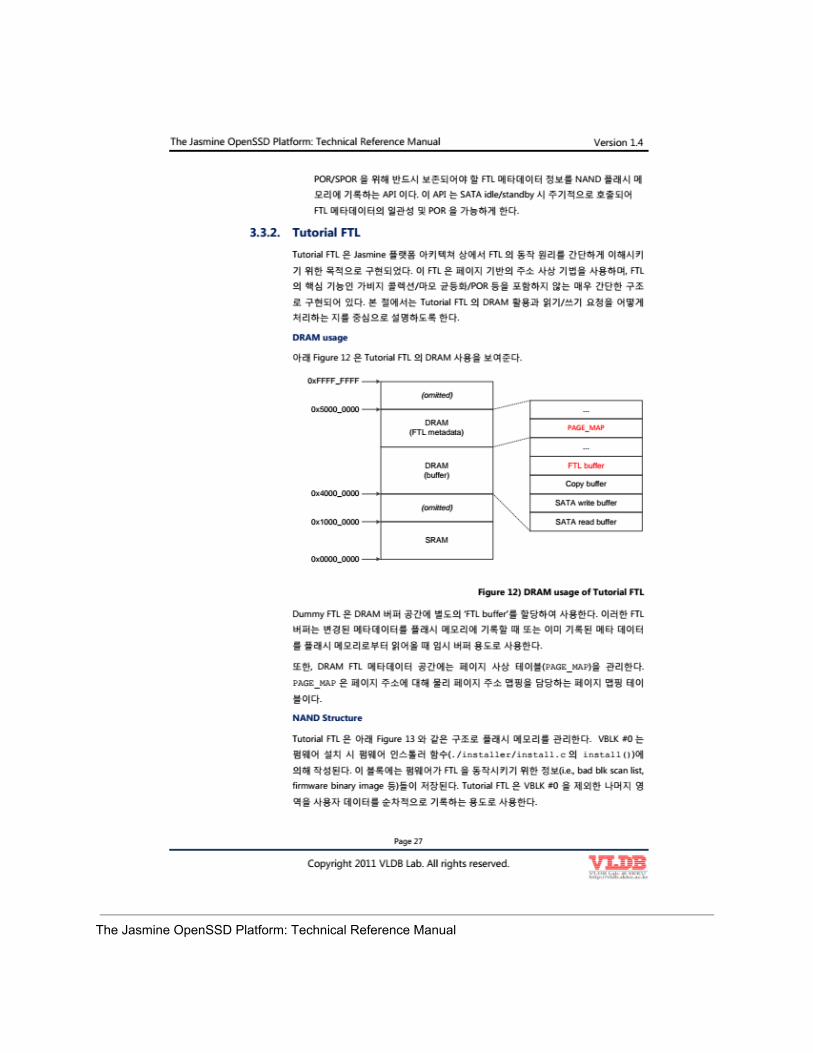
DRAM usage
Figure 12 below shows the use of DRAM Tutorial FTL.
0xFFFF_FFFF
(omitted)(FTL
0x5000_0000
...
DRAM metadata (buffer)12)
DRAMDRAM
) bufferFTLFTL
bufferSATA read
SRAM
0x0000_0000
Figure usage of Tutorial
FTLDummyin the DRAM buffer space is allocated to the separate use of the FTL buffer. This FTL
metadata buffer is changed, or when the flash memory has already been recorded in themetadata
read from the flash memory uses the temporary buffer.
Also, DRAM FTL area has a page mapping table metadata (PAGE_MAP) for managing the.
PAGE_MAP address for the page that is responsible for mapping the physical page addressthe page mapping
oftable.
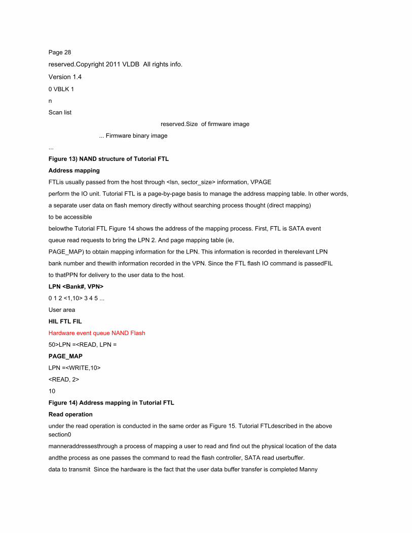
NAND Structure
Tutorial FTL has the same structure as Figure 13 below flash memory management. VBLK # 0the
firmware installer function when installing firmware (. / Installer / install.c the install ())by.
written This block contains information for operating the FTL firmware (ie, bad blk scan list,
firmware binary image, etc.) are stored. Tutorial FTL VBLK # 0, except for the
areathat the user data is written sequentially uses Lab.
Page 27
the.Copyright 2011 VLDB All rights Lab.
PAGE_MAP
...
Copy 0x4000_0000buffer
0x1000_0000
(omitted)
bufferSATA write
Version 1.4

The Jasmine OpenSSD Platform: Technical Reference Manual
Page 28
reserved.Copyright 2011 VLDB All rights info.
Version 1.4
0 VBLK 1
n
Scan list
reserved.Size of firmware image
... Firmware binary image
...
Figure 13) NAND structure of Tutorial FTL
Address mapping
FTLis usually passed from the host through <lsn, sector_size> information, VPAGE
perform the IO unit. Tutorial FTL is a pagebypage basis to manage the address mapping table. In other words,
a separate user data on flash memory directly without searching process thought (direct mapping)
to be accessible
belowthe Tutorial FTL Figure 14 shows the address of the mapping process. First, FTL is SATA event
queue read requests to bring the LPN 2. And page mapping table (ie,
PAGE_MAP) to obtain mapping information for the LPN. This information is recorded in therelevant LPN
bank number and thewith information recorded in the VPN. Since the FTL flash IO command is passedFIL
to thatPPN for delivery to the user data to the host.
LPN <Bank#, VPN>
0 1 2 <1,10> 3 4 5 ...
User area
HIL FTL FIL
Hardware event queue NAND Flash
50>LPN =<READ, LPN =
PAGE_MAP
LPN =<WRITE,10>
<READ, 2>
10
Figure 14) Address mapping in Tutorial FTL
Read operation
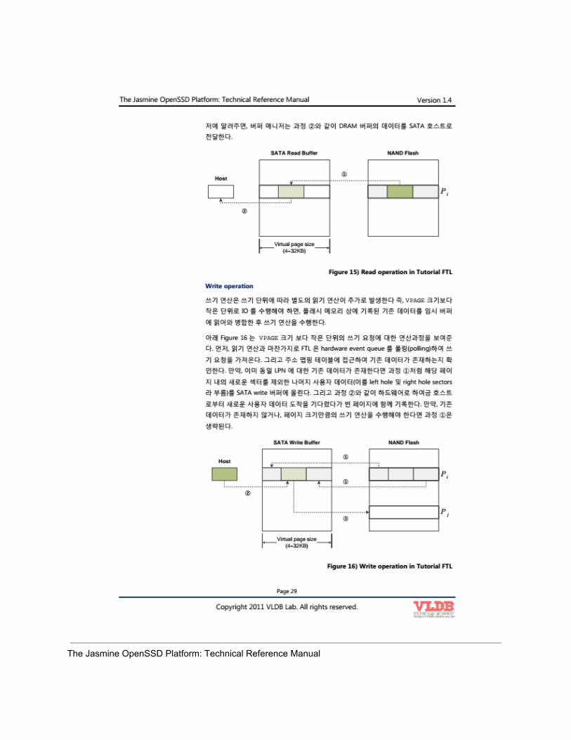
under the read operation is conducted in the same order as Figure 15. Tutorial FTLdescribed in the abovesection0
manneraddressesthrough a process of mapping a user to read and find out the physical location of the data
andthe process as one passes the command to read the flash controller, SATA read userbuffer.
data to transmit Since the hardware is the fact that the user data buffer transfer is completed Manny

The Jasmine OpenSSD Platform: Technical Reference Manual
Page 29
Copyright 2011 VLDB Lab. All rights reserved.
Tells you that the buffer manager as steps 2 and DRAM buffer andthedata to the SATA
transmits host.
SATA BufferRead
NAND Flash
Host
1
i
2
Virtual page size (4 ~ 15)
Read32KB)Figure operation in Tutorial FTL
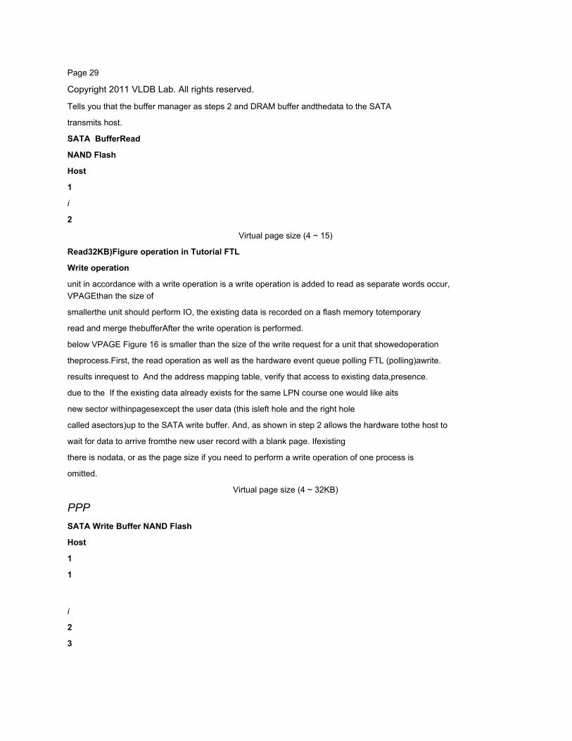
Write operation
unit in accordance with a write operation is a write operation is added to read as separate words occur,VPAGEthan the size of
smallerthe unit should perform IO, the existing data is recorded on a flash memory totemporary
read and merge thebufferAfter the write operation is performed.
below VPAGE Figure 16 is smaller than the size of the write request for a unit that showedoperation
theprocess.First, the read operation as well as the hardware event queue polling FTL (polling)awrite.
results inrequest to And the address mapping table, verify that access to existing data,presence.
due to the If the existing data already exists for the same LPN course one would like aits
new sector withinpagesexcept the user data (this isleft hole and the right hole
called asectors)up to the SATA write buffer. And, as shown in step 2 allows the hardware tothe host to
wait for data to arrive fromthe new user record with a blank page. Ifexisting
there is nodata, or as the page size if you need to perform a write operation of one process is
omitted.
Virtual page size (4 ~ 32KB)
PPPSATA Write Buffer NAND Flash
Host
1
1
i
2
3

j
Figure 16 ) Write operation in Tutorial FTL
Version 1.4

The Jasmine OpenSSD Platform: Technical Reference Manual

Page 30
Copyright 2011 VLDB Lab. All rights reserved.
Version 1.4
Tutorial FTL for the write operation to write the new data to allocate a free pagethe processthe
as much as possiblefor increasingparallelismto be implemented. That is, each write operation on a specificLPN
bankis fixed to not performed, and the bank previously written right after the banktocontinuously
isberecorded.And for the record number of the bank and the VPN information withaddress mapping table
recordedthe(of course, when such a calculation approach of parallelism in terms of sequential read can lose).
Meanwhile, Tutorial FTL during the write operation, the changed metadata separatelyrecorded in the flash
Although notmemory,flash memory fault recovery in order to ensure the meta areaon a regular basis
of metainformationto record changes haejueoya.
BSP Interrupt handling
FTL command is passed to the flash memory exceptions that occur during the process of treatment situations (eg,ECC
errors, runtime bad block occurs, etc.) is treated as a hardware interrupt.
internal flash memory operation error occurs, the BSP interrupt is generated, whichthe flash
corresponds tocontroller interrupt is a hardware interrupt to notify the controller.hardware
ARMinterruptcontroller generates an IRQ interrupt notifies the fact that, ARM IRQ is
interrupthandler(. / Target_spw / misc.c the irq_handler ()) calls.
IRQ interrupts by the interrupt handler, the flash controller (INTR_FLASH) if, FTL
interruptservice routine (ftl_isr) function is called. Since, FTL interrupt register
(BSP_INTR) looking for the source of the error by checking the appropriate exception handling code is executed.
3.3.3. Dummy FTLDummy FTLis to measure the speed of SATA and DRAM as virtual FTL,to the flash memory
without accesspassed from the event queue for handling host requests minimum amount of code
theto be implemented.
Dummy FTL actual implementation (. / ftl_dummy / ftl.c) is, ftl_read / ftl_write
function,reading or writing data to the flash memory does not perform the operation. In other words, SATA and
FTL for normal operation of the SATA read / write buffer to adjust the pointer to the bufferonly operations
to performimplemented.
3.4. Flash Interface LayerFIL is a real FTL IO command is passed to the flash memory by a layer, LLD by
flash command (ie FCP) setting the flash memory in the IO request to the
3.4.1.Flash command issueLLD passed to the IO command is a command transfer function internally Flash (. / Target_spw / flash.c
the flash_issue_cmd ()) into place by. This function is basically set by theLLD

FCP forWR performs a function of transmittingother
the hand, the firmware has three types as below: Table 9 The synchronous / asynchronous IO provides a method
to make good use of these issues to the flash type If you pass on the SSD controller IO IOdisease
ryeolseong can improvetreatment.Lab.

The Jasmine OpenSSD Platform: Technical Reference Manual
Page 31
Copyright 2011 VLDB All rights reserved.
Table 9) FCP issue type
Type Value Description RETURN_ON_ISSUE 0x0
WR WR is empty of content delivery and returns FCPRETURN_ON_ACCEPT 0x1
WR command passed to flash take bank is
whenyou start towaiting (polling) and then returnRETURN_WHEN_DONE
Flash in the corresponding bank0x2,wait until the command is
complete,then return
NOTE: However, flash FTL Hosted by passing the command to wait because the WR command is
another flash in the state must be careful not to deliver orders.
3.4.2 (Lowlevel device driver)LLDLLD,and set the flash command to FCP, FCP is set to pass the WRabstracted
isinterface.This interface allows the developer to the firmware can provide ease of which
implementation,meansthat the IO command to the flash memory for each register is set andflash controller
thewithout having to write code, a flash memory with a logical block page in a simplelogical
can be seen as aarchitecture gazing.
LLD and VBLK are VPAGE unit so that it can perform a flash command implementation. Representative
of (partial) page read / program and block erase, and simple copyback andmodified
acopyback function that is responsible for providing the API.
NOTE: LLD API usage types and more See Section 4.4 of this document
Version 1.4


The Jasmine OpenSSD Platform: Technical Reference Manual
Page 32
Copyright 2011 VLDB Lab. All rights 4.
Version 1.4
reserved.Chapter Jasmine OpenSSD PlatformSoftware SpecificationJasmine OpenSSD This chapter details the software for the platform firmware. Firmware, is
softwarelargely firmware firmware source files and build scripts and installer, and so on. Thisis
chapterthe core module of the firmware for the API described as the center, and includes thefollowinginformation.etc.)
Jasminefirmware file structureJasmine
Firmware APIs (FTL protocol API / LLD API / Memory utility,
Some important macros
4.1 Source File Description
4.1.1. File hierarchyJasmine OpenSSD platform firmware header files and source files can be configured infollowing.
the Description.
Table 10) hierarchy (some files are omitted)File
FileLocationList / Release_lock.inc
COPYING, HISTORY, README
file for debugging scripts, intellectual Property and version history,
Jasmine for a general description of the process of the firmwarebuild. / build_gnu Makefile, ld_script
build.bat
Code Sourcery G+ + toolchain buildusing the
scriptfirmware./ build_rvds armlink_opt.via
file_list.via build.bat
RVDS compile the configuration file and firmware build
script./ ftl_tutorial ftl.h, ftl.c
Tutorial FTL related files folder. / ftl_greedy ftl.h, ftl.c
Greedy FTL related files folder. / ftl_dummy ftl.h, ftl.c
Dummy FTL related files folder. / sata sata_cmd.c
sata_identifiy.c sata_isr.c sata_main.c sata_table.c
SATA interfaces in the Source Files
folder./ installer installer.c,
ata_7.h,installer.sln,ntddstor.h
firmware installation solution file. create install.exe
/ include jasmine.hetc.
file.mem_util.h flash.h, peri.h rom.h,
firmware source code related header
files./ target_spw init_gnu.s, init_rvds.s flash_warpper.c initialize.c target.h mem_util.c, flash.c, uart.c etc.
firmware startup code / firmware initialization /
Memory Utilities / LLD API / UART / Timer
utilities./ tc tc_synth.c
FTL code defined test cases for verification Folder
The Jasmine OpenSSD Platform: Technical Reference Manual
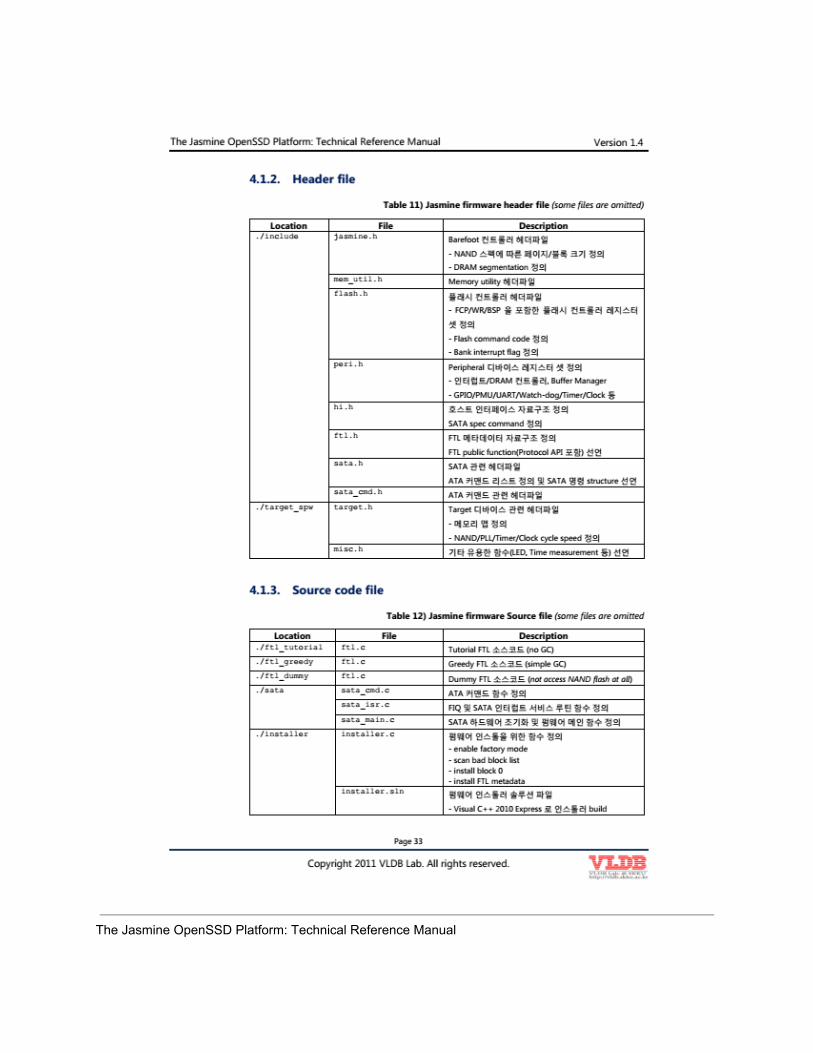
4.1.2. Header filefileTable 11) Jasmine firmware header(some files are omitted)
Location File Description. / Include jasmine.h
Barefoot controller header file
NAND according to the specification page / block size defined
DRAM segmentationdefine mem_util.h
flash header filesMemory utility . h
header files, a flash controller
FCP / WR / BSP, including the flash controller register
set definition
Flash command code definition
Bank interrupt flagdefines peri.h
register set definitionPeripheral devices
Interrupt / DRAM controller, Buffer Manager
GPIO / PMU / UART / Watchdog / Timer / Clock hi.hstructures,such as
host interface data defines
SATA spec commanddefinition ftl.h
the data structure defined in the metadataFTL
FTL public function (Protocol API including)declares sata.h
the relevant header fileSATA
ATA command list sata_cmd.hand SATA commands definedstructuredeclarations.
ATAcommandassociated header file / target_spw target.h
Target devicespecific header files
define the memory map
NAND / PLL / Timer / Clock cycle speed defined misc.h
other useful functions (LED, Time measurement, etc.) Declaration
4.1.3. code Source fileSourcefileTable 12) Jasmine firmware(some files are omitted
Location File Description. / Ftl_tutorial ftl.c
Tutorial FTL source code (no GC). / Ftl_greedy ftl.c
Greedy FTL source code (simple GC). / Ftl_dummy ftl . c
Dummy FTL source code (not access NAND flash at all). / satasata_cmd.c
ATAcommand function definition sata_isr.c
and SATAFIQ interrupt service routinesata_main.cfunction definition
initializes the hardware and firmwareSATAdefines the mainfunction. / installer installer . c
function definition for the firmware installed enable factory mode scan bad block list install block 0 install FTLmetadata installer.sln
firmware installer solution file
Visual C + + 2010 Express installer to build
Page 33
Copyright 2011 VLDB Lab. All rights reserved Lab.reserved.1.4.
Version 1.4Version

The Jasmine OpenSSD Platform: Technical Reference Manual

Page 34
.Copyright 2011 VLDB All rights
/ target_spw initialize.c
firmware initialization function definition
PLL / interrupt / Barefoot controller initializationmem_util.c
flashMemory utility function defined . c
flash memory flash_wrapper.cinitialization andfunction definitions, some
LLDfunction definitions,
FCPpageread / write / copy functions
misc.csuch as delete function block
other useful functionsdefinition LED / NAND block test / Time measurement init_gnu.s init_rvds. s
firmware startup code (GNU /
/ RVDS).tc tc_synth.c
Synthetic test case function definition
Miscellaneous fileDescription.fileTable 13) Jasmine firmware miscellaneous(some files are omitted)
4.1.4.Location File / release_lock.inc
JTAG debug port READEto open a script file
Jasmineand run the firmware build processguidelineson how to
which provides HISTORY
logJasmine COPYINGfirmware revision
Jasmine OpenSSD Platformof the license GPL ver. 3. / Build_rvds armcc_opt.via
armlink_opt.via
RVDS compiler optionssetting
file_list.via
whenfirmware build, compile a list of files subject to
if you will include the newly created filescatter.scl
to compileRVDS, code / ZI / RW data memory address
assignment script. / build_gnu ld_script
GNU tools at compile time, code / ZI / RW data memory
addressassigned to the script
4.2.InstallerFunction InstallerFirmware functions Jasmine The installer (. / Installer / installer.c)operation inFTL
foran initial state to establishperforms a function.
4.2.1. install

installvoid(void)
Function:
Jasmine board perform firmware installed. Operations performed by this function are as follows.
O load scan list o load firmware image o install block # 0 o install FTL metadata

The Jasmine OpenSSD Technical Reference Manual

Platform:NOTE:NAND block when the current firmware version, delete the entire ftl_open In other words,
formatoperationis performed. Jasmine in Normal mode but when initializing the board, response
time out error may occur because, in fact, the install process from within a format.
function, youneed to Also, by installing the initial state of the FTL metadata, Jasmine board bootlater,
time ftl_open function recorded in the flash memory by loading the metadataPOR.
have to enable
4.2.2. ftl_install_mapping_tableftl_install_mapping_tablevoid(void)
Function:
FTL operation, the mapping table including the various kinds of meta datathe initial state of NAND
recorded inflash.The function of the firmware is installed, the mode 'Factory mode'bythe install
invoked while
function, Jasmine metadata recorded in the function board is initialized at boot time FTL
(ftl_open) to be loaded, so, FTL developers ftl_openmodified andwith functions
should beimplemented4.3.
FTLProtocol FTLAPIFTL APIprotocolis passed from the host to initiate the functionsprocessingcommand,
responsible forthe SATA is a function that is called from. These functions are FTL SATA andin order operate witheach other
must be implementedtoto the core API arethis
in section Tutorial FTL (. / Ftl_tutorial / ftl.h) for theofFTL public function in
specificationthe4.3.1.
ftl_openftl_openvoid(void)
Function:
FTL performs initialization. After the device is powered by the first FTL function call.of
The main functionfirmware(. / Target_spw / initialize.c the init_jasmine)
Called by.Carrying out this function, the following operations
o Build scan list o FTL format o FTL metadata initialization 4.3.2. ftl_read
void ftl_read(UINT32 const lba, UINT32 const num_sectors)
Function:
FTL performs a read request. IO is performed in real VPAGE Lab.
Parameter:
Page 35
unit.Copyright 2011 VLDB All rights Lab.
Version 1.4
The Jasmine OpenSSD Platform: Technical Reference Manual
Page 36
reserved.Copyright 2011 VLDB All rights reserved.
Version 1.4
lba given logical sector address from the host
num_sectors number of sectors (512B sector basis)
4.3.3. ftl_writeftl_writevoid(UINT32 const lba, UINT32 const num_sectors)
Function:
FTL performs a write request. IO is performed in real VPAGE unit
Parameter:
lba given logical sector address from the host
num_sectors number of sectors (512B sector basis)
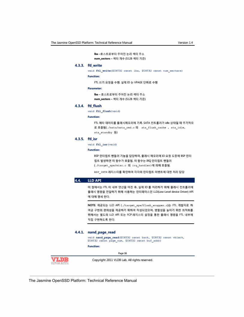
4.3.4. ftl_flushftl_flushvoid(void)
Function:
FTL metadata is written to the flash memory. Idle state, the SATA controllerperiodically
is invoked(. / Sata / sata_cmd.c the ata_flush_cache, ata_idle,
ata_standby, etc.)
4.3.5. ftl_isrftl_isrvoid(void)
Function:
BSP is responsible for the interrupt handler function, flash memory, IO requestduring the BSP
interruptoccursis called with this function. This function is IRQ interrupt handler
(. / Target_spw / misc.c the irq_handler) Called by.
BSP_INTR check the register for each interrupt event handling charge of
4.4. LLD APIThis section describes the internal operations after FTL, in order to handle the actual IOflash controller
flashusing the command interface to deliver a LLD (LowLevel device Driver) API
specification for the.
NOTE: provided LLD API (. / target_spw / flash_wrapper.c) FTL developer to theand
ease of implementationto provide yeogeum written, parallelismto enhance the optimization of
in orderLLD API or FCP separate register set command via the flash within the FTL
to be directly implemented.
4.4.1. nand_page_readnand_page_readvoid(UINT32 const bank, UINT32 const vblock, UINT32 const page_num, UINT32 constbuf_addr)

Function:Platform:
The Jasmine OpenSSD Technical Reference Manual
FCP command (FC_NORMAL_READ_OUT) to a specific page by using the flash read.
memory,perform WR command will be passed to FCP RETURN_WHEN_DONE
Parameter:
bank bank number (max: NUM_BANKS)
vblock VBLK number (max: VBLKS_PER_BANK)
page_num VPAGE number (max: PAGES_PER_BLK)
buf_addr read page data will go upFTL internal buffer
4.4address.two. nand_page_ptreadnand_page_ptreadvoid(UINT32 const bank, UINT32 const vblock, UINT32 const page_num, UINT32 const sect_offset, UINT32 const num_sectors, UINT32 const buf_addr, UINT32 const issue_flag)
Functions:
FCP command (FC_NORMAL_READ_OUT) using a of the flash memorya specific page
portionto readperformed. This function is primarily intended to be used for the following purposes
o recorded in the flash memory when reading metadata (RETURN_WHEN_DONE)
o Partial page program to handleneedto read a particular column of user data
when you (RETURN_ON_ISSUE) Parameter:
bank bank number (max: NUM_BANKS)
vblockVBLK number (max: VBLKS_PER_BANK)
page_num VPAGE number (max: PAGES_PER_BLK)
sect_offset VPAGE the starting sector offset (max: SECTORS_PER_VPAGE)
num_sectors number of sectors (based on a single 512B sector size)
buf_addr FTL climb inside pages read data buffer address
issue_flag FCP flag settings issues. (Refer to Table 9 in Section 3.4.1 of this document)
4.4.3. nand_page_read_to_hostnand_page_read_to_hostvoid(UINT32 const bank, UINT32 const vblock, UINT32 const page_num)
Function:
FCP command (FC_NORMAL_READ_OUT) is useda specific page in the flash memory
to readSATA host interface,pass
and thenthe page read operation, SATA read buffer pointer adjustments performed
Parameter:
bank bank number (max: NUM_BANKS)
vblock VBLK number (max: VBLKS_PER_BANK)
page_num VPAGE number (max: PAGES_PER_BLK)
4.4.4. nand_page_ptread_to_hostPage 37
Copyright 2011 VLDB Lab. All rights Lab.

Version 1.4
The Jasmine OpenSSD Platform: Technical Reference Manual
Page 38
reserved.Copyright 2011 VLDB All rights reserved.
Version 1.4
void nand_page_ptread_to_host (UINT32 const bank, UINT32 const vblock, UINT32 const page_num, UINT32const sect_offset, UINT32 const num_sectors)
Function:
FCP command (FC_NORMAL_READ_OUT) tospecific page in the flash
amemory,read only some sectors ( ie, partial page read), host interfacepassing
page read operation afterSATA,SATA read buffer pointer adjustments performed
Parameter:
bank bank number (max: NUM_BANKS)
vblock VBLK number (max: VBLKS_PER_BANK)
page_num VPAGE number (max : PAGES_PER_BLK)
sect_offset partial read sector offset for the start of VPAGE (max: SECTORS_PER_VPAGE) num_sectors number of sectors (based on a single 512B sector size)
4.4.5. nand_page_programnand_page_programvoid(UINT32 const bank, UINT32 const vblock, UINT32 const page_num, UINT32 constbuf_addr)
Function:
FCP command (FC_NORMAL_IN_PROG) to a specific page in the flash memory
of the FTL writes data to the internal buffer (usually at the time of the metadata records can be used).
Parameter:
bank bank number (max: NUM_BANKS)
vblock VBLK number (max: VBLKS_PER_BANK)
page_num VPAGE number (max: PAGES_PER_BLK)
buf_addr FTL data exists inside a page buffer address.mustVPAGEalign.
be
4.4.6 nand_page_program_from_hostnand_page_program_from_hostvoid(UINT32 const bank, UINT32 const vblock, UINT32 const page_num)
Function:
FCP command (FC_NORMAL_IN_PROG) to a specific page in flash memory using the
SATA write bufferto write data
after the write operationpages, SATA write buffer pointer adjustment
Parameter:
bank bank number (max: NUM_BANKS)
vblock VBLK number (max: VBLKS_PER_BANK)
page_num VPAGE number (max: PAGES_PER_BLK)

4.4.7. nand_page_ptprogram_from_host
The Jasmine OpenSSD Technical Reference ManualFunction:

nand_page_ptprogram_from_hostvoid(UINT32 const bank, UINT32 const vblock, UINT32 const page_num,UINT32 const sect_offset, UINT32 const num_sectors)
Platform:
FCP command (FC_NORMAL_IN_PROG) to a specific page of the flash memoryof my day
partonly record the sector (ie, partial program)
after the page write operation, SATA write buffer adjustment
Parameter:
bank bank number (max: NUM_BANKS)
vblock VBLK number (max: VBLKS_PER_BANK)
page_num VPAGE number (max: PAGES_PER_BLK)
sect_offset partial VPAGE sector offset for the start of the program (max: SECTORS_PER_VPAGE) num_sectors number of sectors (based on a single 512B sector size)
NOTE: In the same page more than once in order to perform partial programming, NAND
flash NOP (Number of Program) to clothing.
4.4.8. nand_page_copybacknand_page_copybackvoid(UINT32 const bank, UINT32 const src_vblock, UINT32 const src_page, UINT32 constdst_vblock, UINT32 const dst_page)
Function:
FCP command (FC_COPYBACK) using the same bank within the page copy
operations.Fast Page DRAM buffer copy is possible because it bypasses
your reference, the following cases are not able to copyback FTL inside the internal
buffer,and then reads the page, the page write operation is performing
o NAND flash memory internal copybackIf you do not support the operation
oof each page is different if the plane Parameter:
bank bank number (max: NUM_BANKS)
src_vblock Original VBLK number (max: VBLKS_PER_BANK)
src_page Original VPAGE number (max: PAGES_PER_BLK)
dst_vblock Copy be VBLK number (max: VBLKS_PER_BANK)
dst_page copied VPAGE number (max: PAGES_PER_BLK)
4.4.9. nand_page_modified_copybacknand_page_modified_copybackvoid(UINT32 const bank, UINT32 const src_vblock, UINT32 const src_page,UINT32 const dst_vblock, UINT32 const dst_page, UINT32 const sect_offset, UINT32 dma_addr, UINT32 constdma_count)
Page 39
Copyright 2011 VLDB Lab. All rights Lab.
Version 1.4
The Jasmine OpenSSD Platform: Technical Reference Manual
Page 40
reserved.Copyright 2011 VLDB All rights reserved.
Version 1.4
Function:
FCP command (FC_MODIFY_COPYBACK) using the same banktheinparticular
to modifydataapage,copy operations.
Note: the following cases, internal modified copyback is not possible inside the FTL
bufferand then reads the page, the page with the new data and performing a write operation
o NAND flash memory internal copyback operation is not supported on the
plane o Each page is a different case
if FC_MODIFY_COPYBACK impossible, by the following procedure modified
copybackoperation is performed:
1.To read this page, DRAM copy buffer Posted
2. Some existing data (left hole) and the destination page inusinga command FC_NORMAL_IN
the flash memory passed
3. The new data to the destination page of the flash memory instruction is passed on FC_IN
4. Existing data on the remaining (right hole) passing the command to FC_IN_PROG, 2, and 3
along with the data in the flash memory programming delivered perform Parameter:
bank bank number (max: NUM_BANKS)
src_vblock Original VBLK number (max: VBLKS_PER_BANK)
src_page Original VPAGE number (max: PAGES_PER_BLK)
dst_vblock copied VBLK number (max: VBLKS_PER_BANK)
dst_page copied VPAGE number (max: PAGES_PER_BLK)
sect_offset will be replaced with the new data sector offset (max: SECTORS_PER_PAGE)
dma_addr new data containing buffer address
dma_count new data size (unit: Byte)
4.4.10. nand_block_erasenand_block_erasevoid(UINT32 const bank, UINT32 const vblock)
Function:
FCP command (FC_ERASE) by using the bank to delete the specific VBLK
note: 1plane mode, the two physical delete Bullock. If the 2plane mode,4
delete the physical block
Parameter:
bank bank number (max: NUM_BANKS)
vblock VBLK number (max: VBLKS_PER_BANK)
4.5. Utility MemoryAPI

MemoryAPIutilitybetween the SRAM and DRAM memory functions for work, and thethis function,
value ofthememory read / write / search, etc. If you need to use.
Memory utility function. / Target_spw / mem_util.c defined in 4.5.1.
The Jasmine OpenSSD Platform: Technical Reference Manual

. _mem_set_sram_mem_set_sramvoid * const UINT32 const val, UINT32 const (ADDR, VAL, BYTES)
(voidaddr,num_bytes)Macro # define mem_set_sram
Function:
SRAM memory value set
Parameter:
ADDR SRAM memory address region and, 4 Byte must be align (max: 0x1000_0000) VAL Setting
BYTES Byte area and you want to set, 4Byte unit which must be
4.5.2. _mem_set_dram_mem_set_dramvoid * const UINT32 const val, UINT32 const (ADDR, VAL, BYTES)
(voidaddr,num_bytes)Macro # define mem_set_dram
Function:
DRAM memory value set in
Parameter:
ADDR DRAM memory address area (min: 0x4000_0000)
VAL Setting
BYTES the area that you want to set Byte, DRAM_ECC_UNITMust be a multiple
4.5.3of._mem_copy_mem_copyvoid * const const void * const src, UINT32 const (DST, SRC, BYTES)
(voiddst,num_bytes)Macro # define mem_copy
Function:
DMA to perform a memory copy. Metadata is often referred to DRAM SRAM
copyand can be used to improve the performance.
Parameter:
DST destination memory address. Must be 4 Bytealign
SRC Source memory address. Must be 4 Bytealign
BYTES byte area, and you want to set, 4Byte unit which must be (max: 32768) (However,
DRAMtoDRAM in the case should be a multiple of DRAM_ECC_UNIT)
4.5.4. _mem_bmp_find_sram_mem_bmp_find_sramUINT32 void * const UINT32 const num_bytes, UINT32 const (BMP, BYTES, VAL)
(constbitmap,val)Macro # define mem_bmp_find_sram
Page 41
Copyright 2011 VLDB Lab. All rights reserved.
Version 1.4
The Jasmine OpenSSD Platform: Technical Reference Manual

Page 42
Copyright 2011 VLDB Lab. All rights reserved.
Version 1.4
Function:
SRAM bit map memory area exists, whether a particular value in the Navigation
Parameter:
BMP bitmap memory address. Must be 4 Bytealign (max: 0x1000_0000)
BYTES byte area, and you want to set, 4 Byte must be a unit (max: UNIT * SIZE = 32768) VAL find a value (mustbe 0 or 1)
Returns:
On success , matching the value of the index number of thein a
failurebitmap,BYTES * 8
4.5.5. _mem_bmp_find_dram_mem_bmp_find_dramUINT32 void * const UINT32 const num_bytes, UINT32 const (BMP, BYTES, VAL)
(constbitmap,val)Macro # define mem_bmp_find_dram
Function:
DRAM bit map memory area exists, whether a particular value in the Navigation
Parameter:
BMP Bit memory address map. Must be 4 Bytealign (min: 0x4000_0000)
BYTES Byte area and you want to set, 4 Byte must be a unit (max: UNIT * SIZE = 32768) VAL looking for value. (0or 1)
Returns:
If successful, the present value of the matchingthe index number of the
fails,bitmap,BYTES * 8
4.5.6. _mem_search_min_max_mem_search_min_maxUINT32 void * const UINT32 const bytes_per_item, UINT32 const size, UINT32 const(ADDR, UNIT, SIZE, CMD)
(constaddr,cmd)Macro # define mem_search_min_max
Function:
Navigation minimum or maximum value in a memory area
Parameter:
ADDR Navigate the memory address. Must be 4 Bytealign
UNIT navigation unit (eg, 1, 2, 4 Byte)
SIZE Navigation index range (max: UNIT * SIZE = 32768)
CMD MU keomaenteu code (eg, MU_CMD_SEARCH_MAX_SRAM, MU_CMD_SEARCH_MIN_SRAM,MU_CMD_SEARCH_MAX_DRAM, MU_CMD_SEARCH_MIN_DRAM )
The Jasmine OpenSSD Technical Reference Manual

Platform:Returns:
On success, the present value of the minimum or maximumindex
failurenumber,SIZE
Example code:
UINT32 0; UINT32 idx; zxcv =
zxcv [100] =[4]0xFFFFFFFF
/ search max value in array 'zxcv' idx = mem_search_min_max (zxcv, sizeof 100, / /
/(UINT32),MU_CMD_SEARCH_MAX_SRAM);ret 4
4.5.7. _mem_search_equ_mem_search_equUINT32 void * const UINT32 const bytes_per_item, UINT32 const size, UINT32 const cmd, UINT32 const (ADDR, UNIT, SIZE, CMD, VAL)
(constaddr,val)Macro # define mem_search_equ
Function:
specific value from a memory area navigation exists
Parameter:
ADDR Navigate the memory address. Must be 4 Bytealign
UNIT navigation unit (eg, 1,2, 4 Byte)
SIZE Navigation index range (max: UNIT * SIZE = 32768)
CMD MU keomaenteu code (eg, MU_CMD_SEARCH_EQU_SRAM, MU_CMD_SEARCH_EQU_DRAM) VAL findThe value
Returns:
On success, the number of matchingindex value
failureexists,SIZE
Example code:
UINT32 UINT32 idx; zxcv =
zxcv [100] = 0;[4]0xFFFFFFFF; / Write data to buffer / /
/search in array idx = mem_search_equ (zxcv, sizeof (UINT32), 100,
0xFFFFFFFF'zxcv' idx = mem_search_equ sizeof 100, /4MU_CMD_SEARCH_EQU_SRAM, / / ret
(zxcv,(UINT32),MU_CMD_SEARCH_EQU_SRAM, 0xFFFFFFFF);/ret0x80808080);100
Notes:
Memory utility (DMA) to take advantage of, DRAM 32KByte 4Byte particular value when navigating in the area,
it takes a maximum of about 180us (ie, 177MB / s. stage, SATA, or access data from the DRAMNAND
tocase, can be slower )
Page 43
Copyright 2011 VLDB Lab. All rights Lab.
Version 1.4
The Jasmine OpenSSD Platform: Technical Reference Manual

Page 44
reserved.Copyright 2011 VLDB All rights 4.5.8.
Version 1.4

The Jasmine OpenSSD Platform: Technical Reference Manual
reserved. _mem_cmp_sram_mem_cmp_sramUINT32 void * const const void * const addr2, const UINT32 (ADDR1, ADDR2, BYTES)
(constaddr1,num_bytes)Macro # define mem_cmp_sram
Function:
SRAM performs comparison of two memory areas
Parameter:
ADDR1 the first memory address. Must be 4 Bytealign (max: 0x1000_0000)
ADDR2 second memory address. Must be 4 Bytealign (max: 0x1000_0000)
BYTEScomparison range
Returns:
the same,it returns
different,0,1 or 1 to return
4.5.9. _mem_cmp_dram_mem_cmp_dramUINT32 void * const const void * const addr2, const UINT32 (ADDR1, ADDR2, BYTES)
(constaddr1,num_bytes)Macro # define mem_cmp_dram
Function:
DRAM performed comparing the two memory areas. This function is nonDMAthe CPUdatadirectlyDRAM
andreads comparing
Parameter:
ADDR1 starting memory address. Must be 4 Bytealign (min: 0x4000_0000)
ADDR2 starting memory address. Must be 4 Bytealign (min: 0x4000_0000)
BYTES Compare the range
Returns:
the same,it returns
different,0,1 or 1returns.
4.5.10 _read_dram_8_read_dram_8UINT8 constaddr)(ADDR)
(UINT32 Macro # define read_dram_8
Function:
DRAM to SRAM of 8 bit (1 Byte) to the CPU is directly read from the memory address ohm.
Parameter:
ADDR DRAM memory address to read
Returns:
Page 45
Copyright 2011 VLDB Lab. All rights Lab.
Version 1.4

The Jasmine OpenSSD Platform: Technical Reference Manual
Page 46
reserved.Copyright 2011 VLDB All rights reserved.
Version 1.4
DRAM memory data values read from the 8bit
4.5.11. _read_dram_16_read_dram_16UINT8 const (ADDR)
(UINT32addr)Macro # define read_dram_16
Function:
DRAM to SRAM, 16 bit (2 Bytes) and the CPU is directly read from the memory address
ohm.
Parameter:
ADDR DRAM memory address to read
Returns:
DRAM memory data values read from a 16 bit
4.5.12. _read_dram_32_read_dram_32UINT8 const (ADDR)
(UINT32addr)Macro # define read_dram_32
Function:
DRAM to SRAM, 32 bit (4 Byte) to the CPU is directly read from the memory address ohm.
Parameter:
ADDR DRAM memory address to read. Must be 4 Bytealign
Returns:
DRAM memory data values read from a 32bit
4.5.13. _write_dram_8_write_dram_8void const UINT32 const (ADDR, VAL)
(UINT32addr,val)Macro # define write_dram_8
Function:
mem_copy function on DRAM memory addresses using 8 bit (1 Byte) to record data
(internallyalign the For debugging, memory addresses, so it should be noted)
Parameter:
ADDR the address to write data to the DRAM memory (min: 0x4000_0000)
VAR 8 bit data
4.5.14. _write_dram_16_write_dram_16void const UINT32 const (ADDR, VAL)
(UINT32addr,val)Macro # define write_dram_16
Function:Platform:

The Jasmine OpenSSD Technical Reference Manual

mem_copy function to DRAM memory address on 16 bit (2 Bytes) of data to
record.(Internally, the relative address to align so that the memory debugging Note)
Parameter:
ADDR the address to write data to the DRAM memory (min: 0x4000_0000)
VAR 16 bit data
4.5.15. _write_dram_32_write_dram_32void const UINT32 const (ADDR, VAL)
(UINT32addr,val)Macro # define write_dram_32
Function:
mem_copy function to DRAM memory address on 32 bit (4 Bytes) to data
record
Parameter:
ADDR data, DRAM memory address to write. Must be 4 Bytealign (min: 0x4000_0000) VAR 32 bit data
4.5.16. _set_bit_dram_set_bit_dramvoid const UINT32 const (BASE_ADDR, BIT_OFFSET)
(UINT32base_addr,bit_offset)Macro # define set_bit_dram
Function:
DRAM memory offset to a specific one bit SET
Parameter:
BASE_ADDR DRAM base address
BIT_OFFSET BASE_ADDR standard bit offset
4.5.17 . _clr_bit_dram_clr_bit_dramvoid const UINT32 const (BASE_ADDR, BIT_OFFSET)
(UINT32base_addr,bit_offset)Macro # define clr_bit_dram
Function:
DRAM memory offset to a specific one bit UNSET (CLEAR)
Parameter:
BASE_ADDR DRAM base address
BIT_OFFSET BASE_ADDR bit offset standards
4.5.18. _tst_bit_dram_tst_bit_dramBOOL32(UINT32 const base_addr, UINT32 const bit_offset)
Page 47
Copyright 2011 VLDB Lab. All rights reserved.
Version 1.4
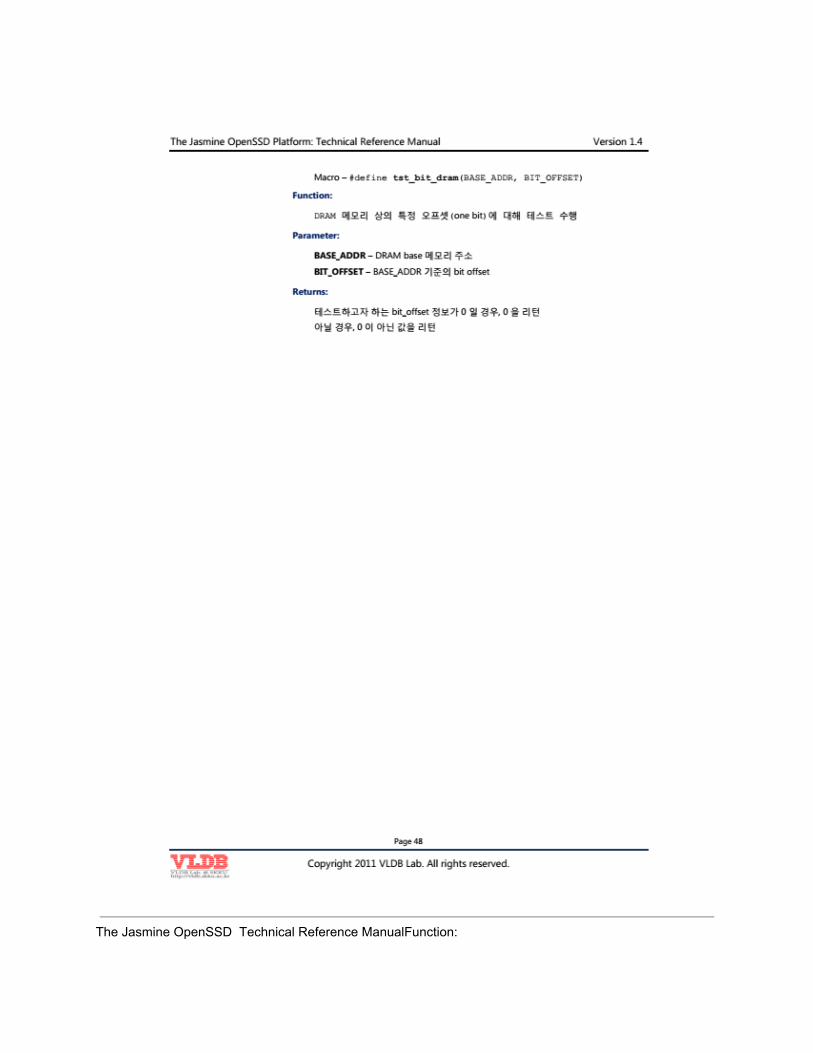
The Jasmine OpenSSD Technical Reference ManualFunction:

Macro # define tst_bit_dram (BASE_ADDR, BIT_OFFSET)
Platform:
DRAM memory on a specific offset (one bit) to perform a test
Parameter:
BASE_ADDR DRAM base memory address
BIT_OFFSET BASE_ADDR Based on the bit offset
Returns:
bit_offset information you want to test is 0, returns 0
if not, it returns a nonzero value,
Page 48
Copyright 2011 VLDB Lab. All rights reserved.
Version 1.4