
THE GROWTH AND CHARACTERIZATION OF Fe/TaO /Co...
74
THE GROWTH AND CHARACTERIZATION OF Fe/TaO x /Co MULTILAYERS FOR SPINTRONICS APPLICATIONS A Thesis Submitted to the Graduate School of Engineering and Sciences of İzmir Institute of Technology in Partial Fulfillment of the Requirements for the Degree of MASTER OF SCIENCE in Physics by Hüseyin TOKUÇ July 2008 İZMİR
Transcript of THE GROWTH AND CHARACTERIZATION OF Fe/TaO /Co...
THE GROWTH AND CHARACTERIZATION OF Fe/TaOx/Co MULTILAYERS FOR SPINTRONICS
APPLICATIONS
A Thesis Submitted to the Graduate School of Engineering and Sciences of
İzmir Institute of Technology in Partial Fulfillment of the Requirements for the Degree of
MASTER OF SCIENCE
in Physics
by
Hüseyin TOKUÇ
July 2008 İZMİR

ii
We approve the thesis of Hüseyin TOKUÇ _______________________________ Assist. Prof. Dr. Süleyman TARI Supervisor _______________________________ Assoc. Prof. Dr. Hakan KÖÇKAR Committee Member Assoc. Prof. Dr. Salih OKUR Committee Member 7 July 2008 Date ______________________________ Prof. Dr. Durmuş Ali DEMİR Prof. Dr. Hasan BÖKE Head of Physics Department Dean of the Graduate School of Engineering and Science
ACKNOWLEDGEMENTS
I would like to thank to my advisor Assist. Prof. Dr. Süleyman TARI for his
motivation, academic guidance and positive attitude during my master degree.
I would like to thank to Assoc. Prof. Dr. Salih OKUR for AFM and Dr. Gülnur
Aygün for ellipsometry measurements. I acknowledge the Center of Material Research
of İzmir Institute of Technology for X-Ray measurements and Department of Physics
for providing Teaching Assistantship. I also thank to İzmir Institute of Technology for
providing Research Assistantship and TUBITAK for funding the project ‘‘TBAG-
105T109’’ during my thesis.
I am very thankful to Dr. İlbeyi Avcı, Berrin P. Algül and Barış Pekerten for
their help during my study.

iv
ABSTRACT
THE GROWTH AND CHARACTERIZATION OF Fe/TaOx/Co
MULTILAYERS FOR SPINTRONICS APPLICATIONS
In this thesis, the effect of Ta buffer layer and the thickness of the Ta2O5 barrier
layer on the structural and magnetic properties of Fe/Ta2O5/Co multilayers have been
studied. XRD and AFM techniques were used for structural investigations and VSM
was used for investigation of magnetic properties. Refractive index of the barrier layer
was determined by ellipsometry technique. In this study, magnetic tunnel junctions
have also been fabricated by using photolithography technique and then electrical and
magnetoresistance measurements were done.
The structural investigations showed that Ta under layer increases the crystalline
quality of Fe layer and causes a change on magnetic parameters of Fe films. The AFM
results showed that the range of the roughness for all layers is between 1.7 Å and 6.3 Å.
When the thickness of the oxide layer was 4 nm, magnetic decoupling appears. Clear
differences between the coercive fields of the ferromagnetic layers were observed in
further increase of the barrier layer thickness. The effect of annealing on the
Fe/TaOx/Co multilayer was studied and it was found that only the coercivity of Fe film
increases with increasing temperature up to the 250°C. Then, annealing at 400°C
showed a sharp decrease in the coercivity of Fe film indicating an intermixing at the
interface of Fe/TaOx. Co minor loops showed that the magnetostatic coupling is large
for thin barriers and decreases with increasing the barrier thickness. Electrical
measurements showed that conduction occurs via tunneling electrons. However, no
TMR ratio has been observed after magnetoresistance measurements.
v
ÖZET
SPİNTRONİK UYGULAMALARI İÇİN Fe/TaOx/Co ÇOKLU
KATMANLARININ BÜYÜTÜLMESİ VE KARAKTERİZASYONU
Bu tezde, Ta alt tabakası ile Ta2O5 yalıtkan oksit tabakasının kalınlığının,
Fe/TaOx/Co çoklu katmanlarının yapısal ve manyetik özellikleri üzerindeki etkileri
incelenmiştir. Yapısal incelemelerde XRD ve AFM teknikleri, manyetik incelemelerde
VSM ve oksit tabakasının kırılma indisinin ölçümünde de elipsometri teknikleri
kullanılmıştır. Bu çalışmada ayrıca manyetik tünel eklemleri fotolitografi tekniğiyle
üretilmiş ve sonra elektriksel ve manyetik-direnç ölçümleri yapılmıştır.
Yapısal incelemeler, Ta alt katmanının, Fe’ in kristal özelliğini arttırdığını ve
manyetik özelliklerinin değişmesine yolaçtığını göstermiştir. Yapılan AFM
ölçümlerinde katmanların yüzey prüzlülüklerinin 1.7 Å ile 6.3 Å arasında değiştiği
gözlenmiştir. Oksit tabakasının kalınlığı 4 nm olduğunda manyetik etkileşimsizlik
gözlenmeye başlanmıştır. Oksit tabakasının kalınlığı arttırılmaya devam ettirildiğinde,
ferromanyetik tabakaların coersivite alanları arasındaki fark açıkça gözlenmeye
başlanmıştır. Tavlamanın çoklu katman üzerindeki etkisi araştırılmış ve Fe/TaOx/Co
çoklu katmanının 250°C’ye kadar tavlanması, sadece Fe katmanının coersivite alanının
arttığını göstermiştir. 400°C de tavlama, coercivite alanında keskin bir düşüşe neden
olmuştur. Bu, Fe/TaOx ara yüzeyinde bir oksijen karışımın olduğunu göstermiştir. Co
minor histeresis eğrileri, ince oksit tabakası için manyetostatik etkileşimin büyük
olduğunu ve oksit tabakasının kalınlığı arttıkça etkileşimin azaldığını göstermiştir.
Elektriksel ölçümler iletimin tünelleme yapan elektronlar tarafında oluştuğunu
göstermiştir. Ancak, manyetik ölçümlerin sonunda TMR oranı gözlenememiştir.

vi
TABLE OF CONTENTS
LIST OF FIGURES ....................................................................................................... viii
LIST OF TABLES........................................................................................................... xi
CHAPTER 1. INTRODUCTION .................................................................................. 1
CHAPTER 2. MAGNETISM ........................................................................................ 7
2.1. The origin of Magnetism ...................................................................... 7
2.2. Types of Magnetism ............................................................................. 9
2.2.1. Diamagnetism ................................................................................. 9
2.2.2. Paramagnetism................................................................................ 9
2.2.3. Ferromagnetism ............................................................................ 10
2.3. Exchange Interaction .......................................................................... 11
2.3.1. Direct Exchange............................................................................ 12
2.3.2. Indirect Exchange ......................................................................... 13
2.3.3. Superexchange .............................................................................. 14
2.4. Magnetic Domains.............................................................................. 15
2.5. Magnetic Anisotropy .......................................................................... 16
2.5.1. Magnetocrystalline Anisotropy..................................................... 16
2.5.2. Shape Anisotropy.......................................................................... 18
2.5.3. Exchange Anisotropy.................................................................... 19
2.6. Tunneling Magnetoresistance ............................................................. 20
2.7. Coupling Mechanism in TMR Spin Valve Structures ........................ 24
2.7.1. Pinhole Coupling .......................................................................... 25
2.7.2. Neel Coupling ............................................................................... 25
2.7.3. Neel Wall Coupling ...................................................................... 26
CHAPTER 3. MATERIAL PROPERTIES ................................................................. 28
3.1. Iron (Fe) .............................................................................................. 28
3.2. Cobalt (Co) ......................................................................................... 29

vii
3.3. Tantalum (Ta) and Tantalum-oxide (TaOx)........................................ 30
CHAPTER 4. EXPERIMENTAL TECHNIQUES...................................................... 31
4.1. Magnetron Sputtering ......................................................................... 31
4.2. Characterization Techniques............................................................... 33
4.2.1. X-ray Diffractometer (XRD) ....................................................... 33
4.2.2. Atomic Force Microscopy (AFM)................................................ 35
4.2.3. Ellipsometry.................................................................................. 35
4.2.4. Vibrating Sample Magnetometer (VSM) ..................................... 36
4.2.5. Electrical and Magnetoresistance Measurements ......................... 37
CHAPTER 5. RESULTS AND DISCUSSION ........................................................... 39
5.1. X-ray Diffraction Results.................................................................... 39
5.1.1. SiO2/Fe.......................................................................................... 39
5.1.2. SiO2/Ta/Fe ................................................................................... 40
5.1.3. SiO2/Ta/Fe/TaOx .......................................................................... 41
5.2. Atomic Force Microscopy .................................................................. 42
5.2.1. SiO2/Ta.......................................................................................... 42
5.2.2. SiO2/Fe and SiO2/Ta/Fe ................................................................ 44
5.3. Vibrating Sample Magnetometer........................................................ 46
5.3.1. SiO2/Fe ......................................................................................... 46
5.3.2. SiO2/Ta/Fe.................................................................................... 47
5.3.3. SiO2/Co and SiO2/Ta/Co............................................................... 48
5.3.4. SiO2/Ta/Fe, SiO2/Ta/Fe/Ta and SiO2/Ta/Fe/TaOx ....................... 50
5.3.5. SiO2/Ta/Fe/TaOx .......................................................................... 51
5.3.6. SiO2/Ta/Fe/TaOx/Co .................................................................... 52
5.4. Annealing Effect on SiO2/Ta/Fe/TaOx/Co ......................................... 55
5.5. Electrical and Magnetoresistance Measurements ............................. 56
CHAPTER 6. CONCLUSION..................................................................................... 58
REFERENCES ............................................................................................................... 60
viii
LIST OF FIGURES
Figure Page
Figure 1.1. A typical GMR spin valve structure............................................................. 2
Figure 1.2. The figure of conduction in a GMR structure. ............................................. 3
Figure 1.3. Magnetoresistance Curve for Fe/Cr multilayer at low
temperatures................................................................................................. 4
Figure 2.1. Relationship between magnetic dipole moment and orbital
motion of an electron. .................................................................................. 7
Figure 2.2. The Hysteresis Loop of a Ferromagnet...................................................... 11
Figure 2.3. Antiparallel alignment for small interatomic distances. ............................ 12
Figure 2.4. Parallel alignment for large interatomic distances..................................... 12
Figure 2.5. The Bethe-Slater curve .............................................................................. 13
Figure 2.6. Indirect exchange versus the interatomic distance .................................... 13
Figure 2.7. Two transition ions couples each other antiferromagnetically
via an oxygen ion....................................................................................... 14
Figure 2.8. Formation of new domains causes decreasing of the energy
within the stray fields ................................................................................ 16
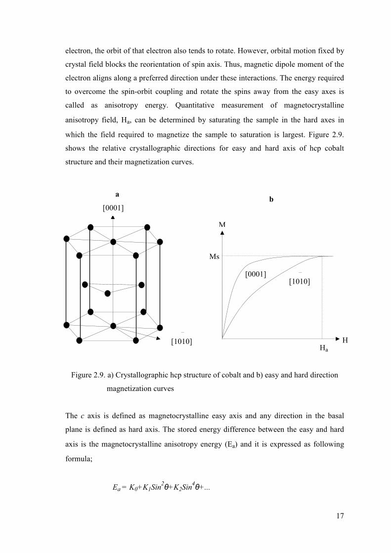
Figure 2.9. a) Crystallographic hcp structure Co ......................................................... 17
Figure 2.9. b) Easy and hard magnetization direction curves of hcp Co ..................... 17
Figure 2.10. The demagnetizing field produced by surface pole distribution ................ 19
Figure 2.11. Schematic representation of spins dynamic in AFM/FM
exchange biased system. ............................................................................ 20
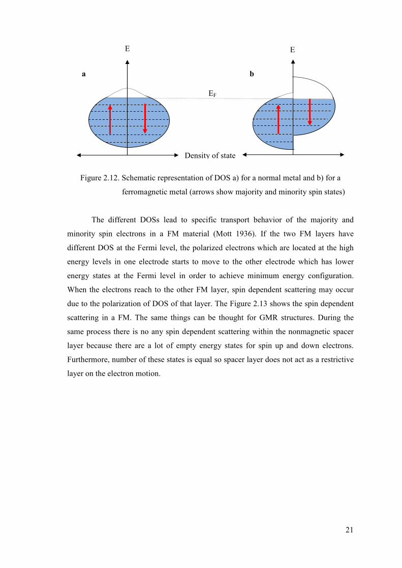
Figure 2.12. a) Schematic representation of DOS for a normal metal............................ 21
Figure 2.12. a) Schematic representation of DOS for a ferromagnetic metal ................ 21
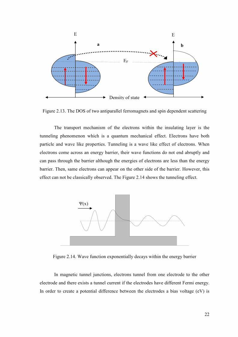
Figure 2.13. The DOS of two antiparallel ferromagnets and spin dependent
scattering.................................................................................................... 22
Figure 2.14. Wave function exponentially decays within the energy barrier.. ............... 22
Figure 2.15. Band diagram of metal/insulator/metal structure .. .................................... 23
Figure 2.16. Small pinholes inside the encircled regions causes the coupling
through the very thin nonmagnetic layer ................................................... 25
Figure 2.17. The roughness induced Neel coupling ...................................................... 26
ix
Figure 2.18 a) Induced stray field on domain boundaries. Orientations
inside the walls tend to be opposite in order to reduce dipole-
dipole interaction energy for each domains . ............................................. 27
Figure 2.18. b) Neel wall coupling between the two magnetic layers .......................... 27
Figure 3.1. Bcc crystalline structure of bulk iron and arrangements of
atomic dipole moments due to the ferromagnetic coupling....................... 28
Figure 3.2. Fcc cubic structure of cobalt ..................................................................... 29
Figure 3.3. Bcc and tetragonal structures of tantalum ................................................. 30
Figure 4.1. Magnet configuration and magnetic field lines of a magnetron
head............................................................................................................ 32
Figure 4.2. ATC Orion 5 UHV Sputtering System.. .................................................... 33
Figure 4.3. X-ray diffraction . ...................................................................................... 34
Figure 4.4. (a) The FWHM for a real XRD peak......................................................... 35
Figure 4.4. (b) The FWHM for an ideal XRD peak..................................................... 35
Figure 4.5. Lakeshore 7400 Vibrating Sample Magnetometer . .................................. 37
Figure 4.6. I-V program for electrical measurements .................................................. 38
Figure 4.7. R-H program for magnetoresistance measurements.................................. 38
Figure 5.1. The XRD patterns of Fe films for various thicknesses ............................. 40
Figure 5.2. The XRD pattern of Ta(24nm)/Fe(12nm) and Fe (12nm)
grown on SiO2............................................................................................ 41
Figure 5.3. XRD diffraction peak of the Fe film with different buffer layer
thicknesses.. ............................................................................................... 42
Figure 5.4. AFM images of 6 nm thick Ta thin film ................................................... 43
Figure 5.5. AFM images of 36 nm thick Ta thin film.................................................. 43
Figure 5.6. Rms roughness of SiO2/Ta and SiO2/Fe single layers . ............................. 44
Figure 5.7. AFM images of 12 nm Fe film on SiO2 substrate .. .................................. 45
Figure 5.8. AFM images of 72 nm Fe film on SiO2 substrate.. ................................... 45
Figure 5.9. AFM images of Ta(24nm)/Fe(12nm) on SiO2 substrate . ......................... 45
Figure 5.10. The hysteresis loops of Fe thin film with different thicknesses
on SiO2....................................................................................................... 47
Figure 5.11. The effect of Ta buffer layer on the magnetic properties of Fe
layer. .......................................................................................................... 48
Figure 5.12. The angle dependent hysteresis curves of SiO2/Co(8nm). ........................ 49
Figure 5.13. The angle dependent hysteresis curves of SiO2/Ta/Co(8nm).................... 49
x
Figure 5.14. The effects of Ta and TaOx capping layers on the Hc of Fe
film............................................................................................................. 50
Figure 5.15. VSM measurements of SiO2/Ta(d)/Fe(12nm)/TaOx structure
with different Ta buffer layer..................................................................... 51
Figure 5.16. The Hysteresis loops of full spin valve stack layer with different
TaOx thicknesses......................................................................................... 52
Figure 5.17. Ellipsometry measurements of TaOx single layers..................................... 53
Figure 5.18. The minor loops of Co free layer on the Full MTJ stack layers................. 54
Figure 5.19. Hysteresis curves of SiO2/Ta/Fe/TaOx(13nm)/Co stack layer................... 55
Figure 5.20. Non-linear I-V characteristics of SiO2/Ta/Fe/TaOx(13nm)/Co
/Ta MTJ stack layer. ................................................................................... 56
Figure 5.21. Fitted J-V curve of SiO2/Ta/Fe/TaOx(13nm)/Co/Ta MTJ stack
layer ........................................................................................................... 57

xi
LIST OF TABLES
Table Page
Table 2.1. Curie temperature of some ferromagnetic materials..................................... 10
Table 2.2. Critical sizes of some spherical magnetic materials with no
shape anisotropy. .......................................................................................... 15

1
CHAPTER 1
INTRODUCTION
Magnetism is widely used in many research areas not only as a scientific branch
but also due to its great application areas such as magnetic sensors and magnetic
memories. The computer technology has been one of the most important areas of the
application of magnetism, recently. In the 21st century, technological development
requires denser, faster and smaller electronic devices as well as low power consumption
in order to improve the functionalities. These requirements bring about using the spin
property of the electrons in devices hence the name spintronics.
Spin is an intrinsic property of electrons and it is a purely quantum mechanical
phenomena. Electrons have two different spin states, spin up and spin down. Using this
property, it is possible to build devices in which the spin property of electrons is
controlled. Spintronic devices have small operation size which can offer high storage
information and faster operation speed because direction of spins can switch on the
order of nano second. Moreover, spintronic devices such as MRAMs are non-volatile,
that is when the power goes off, spins can keep their magnetization directions while in
the conventional devices such as in DRAMs, capacitors lose their charges and memory
assemblies refresh the all chips about 1000 times within a second by reading and re-
writing the contents of the all chips. This situation requires a constant power supply,
which is the reason why DRAMs lose their memory when power turns of. However, the
MRAMs do not need the refreshing at any time and continuous power to keep the
information. All these things offer that spintronics is an attractive research area for the
storage information industry.
The effect of spin on the electrical resistance was firstly observed by Thomson
(1856). He demonstrated that the electrical resistance of a ferromagnetic conductor
depended on whether the current flowing through the conductor was perpendicular or
parallel to the magnetization of the sample. When the current flows parallel to the
magnetization vector of the sample, the strong scattering process occurs and high
resistance is observed, ρ||. However, when the current and magnetization vector are
perpendicular to each other, low scattering and low resistivity are observed, ρ. This

2
event has been called as anisotropic magnetoresistance effect (AMR). Although the
AMR effect previously shows the relationship between spin and electrical resistance,
the discovery of Giant Magnetoresistance (GMR) effect is considered as the birth of the
spintronics. It was independently discovered for Fe/Cr/Fe trilayers (Binasch, et al.
1989) and for Fe/Cr multilayers (Baibich, et al. 1988). A typical GMR device consists
of two ferromagnetic layers (FM) separated by a nonmagnetic (NM) spacer layer which
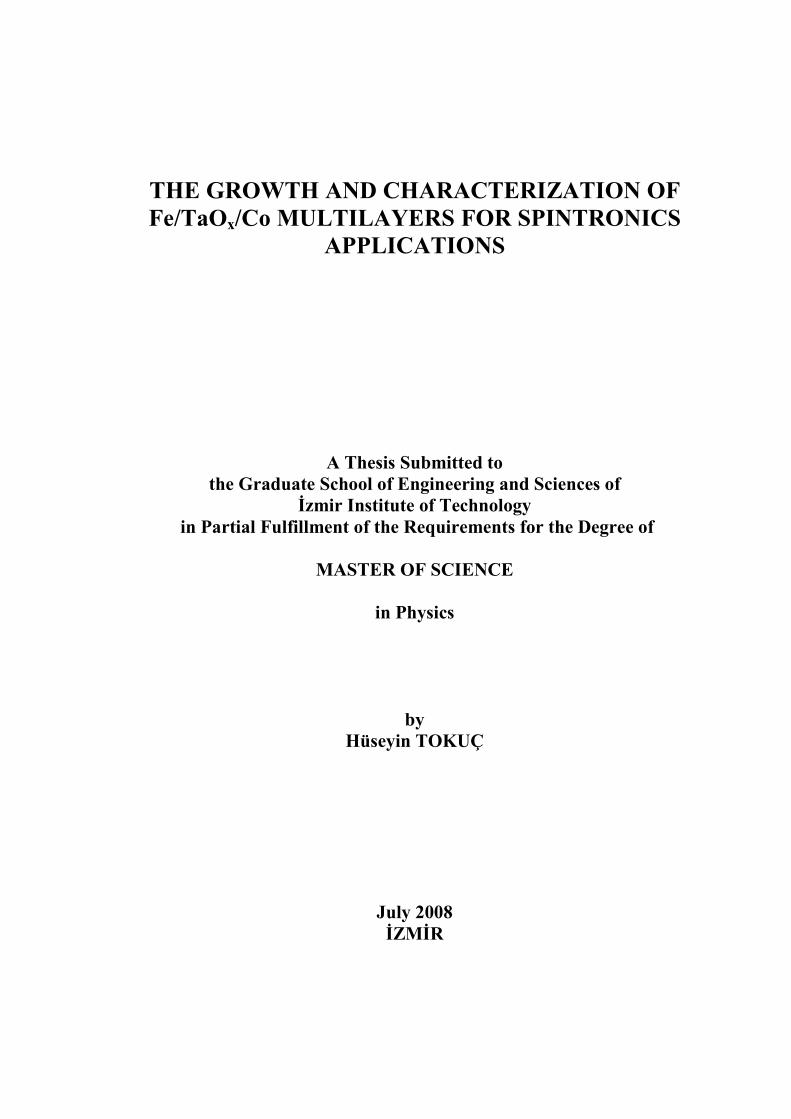
behaves as a spin valve. The schematic of spin valve structure is shown in Figure 1.1.
Figure 1.1. A typical GMR spin valve structure.
Operation principle of these devices depends on the relative alignment of
magnetizations of the two FM layers one of which is pinned while the other one is free
to rotate under external magnetic field. If the magnetization directions of the magnetic
layers are antiparallel, the system shows high resistance. When they are aligned
parallel, the resistance reaches its minimum value. The Figure 1.2 summarizes the
operation principle of a simple GMR structure. In the Figure 1.2a, only the spin up
electrons can pass without any scattering through the whole structure and spin down
electrons scatter within the both layer then conduction is supplied by spin up electrons.
However, in the Figure 1.2b, while only the spin down electrons scatter within the first
layer, the spin up electrons do not scatter and for the second FM layer vice versa then
system has a big resistance. The significant change of the resistance has been called as
giant magnetoresistance and the value of the GMR is calculated by the following
formula;
I
FM NM FM

3
where R↑↓ and R↑↑ are the resistances of antiparallel and parallel alignment,
respectively.
Figure 1.2. The figure of conduction in a GMR structure a) in parallel alignment and b)
in antiparallel alignment.
The variation of the resistance from antiparallel to parallel configuration as a
function of the applied magnetic field was observed for the Fe/Cr multilayers shown in
Figure 1.3.
FM NM FM FM NM FM
(a) (b)
100)( xR
RRGMR
↑↑
↑↑↑↓ −=

4
Figure 1.3. Magnetoresistance curve for Fe/Cr multilayers at low temperature.
The development of the spintronics has been going on with the discovery of
tunneling magnetoresistance (TMR) effect. A simple TMR device consists of two FM
layers which are separated by a NM insulating spacer layer. In the TMR devices,
insulating layer should be very thin so that electrons can tunnel easily without any
scattering which can cause changing the orientation of spins. The thickness of the
insulating layers generally is about 1-2 nm (Hehn, et al. 2000). The operation principle
of the TMR devices is the same with GMR devices and based on the relative alignment
of the FM electrodes. However, the physical origin of TMR depends on the quantum
mechanical tunneling phenomena of the wave function of electrons. The TMR ratio is
defined as following formula;
100)( xR
RRTMR
↑↑
↑↑↑↓ −=
Although the first experiment reported by Julliere (1975) at low temperature
showed 14% TMR ratio for Co/oxidized Ge/Fe junctions, the significant change in the
magnetoresistance at room temperature was observed for CoFe/Al2O3/Co junctions with
TMR ratio of 11% (Moodera, et al. 1995) and Fe/Al2O3/Fe junctions with TMR ratio of
20% (Miyazaki and Tezuka 1995), where Al2O3 insulating layers were amorphous.
Since that time scientists have been trying to improve TMR ratios of magnetic tunnel
5
junctions by using different ferromagnets (Fe, Co, Ni alloys) and some physical
treatments. One of the most widely using methods is annealing process of the
multilayers. Annealing of the multilayers under the suitable conditions almost doubles
the TMR ratio (Sousa, et al. 1998). Furthermore, polycrystalline CoFe (Han, et al.
2000) and amorphous CoFeB (Wang, et al. 2004) electrodes show the TMR ratio of
50% and 70%, respectively. The other method in order to obtain high TMR ratio is to
use of electrodes which have higher spin polarization at the Fermi level. This type of
electrodes shows half metallic behavior such as CrO2, Fe3O4, La0.7Sr0.3MnO3,
La0.7Ca0.3MnO3, Sr2FeMoO6 types and Heusler alloys like NiMnSb or Co2MnSi (Alain
and Daniel 2005). By using these types of electrodes, it has been possible to obtain very
large TMR ratios at low temperatures. However, TMR ratio decreases and vanishes at
near the room temperature for these electrodes (Bowen, et al. 2003). The last method in
order to achieve high TMR ratios is using the crystalline MgO barrier instead of
amorphous Al2O3 spacer layer. It is well known that crystalline structures have perfect
ordered atoms in space and the number of structural defects is less than amorphous
materials. Using a crystalline MgO barrier results in low scattering at the barrier layer
with respect to amorphous layers and spins can keep their orientations. Thus, it is easy
to obtain large TMR ratios with respect to the MTJs with amorphous Al2O3 barrier. The
first experimental results about MgO barrier were reported for Fe/MgO/FeCo(001)
multilayer and the TMR ratio was 60% at low temperature and it was very large when
comparing to the same structure with amorphous barrier (13% at that temperature)
(Bowen, et al. 2001). Then, dramatic increase in TMR ratio with MgO barrier has been
observed in Fe/MgO/Fe single crystalline multilayer by using molecular beam epitaxy
(MBE). The TMR ratio of 250% at low temperature and 180% at room temperature
were observed (Yuasa, et al. 2004). Also 300% and 220% TMR ratios have been
obtained for CoFe/MgO/CoFe polycrystalline multilayer after thermal annealing
(Parkin, et al. 2004). Furthermore, Djayaprawira, et al. (2005) obtained 300% at low
temperature and 230% at room temperature with CoFeB/MgO/CoFeB multilayer grown
by magnetron sputtering, where CoFeB layers are amorphous but MgO layer is (001)
textured. Finally, TMR ratio was achieved the value of %500 for CoFeB/MgO/CoFeB
at room temperature (Lee, et al. 2007). Hence, single crystalline MgO has been widely
used as a barrier layer in many magnetic tunnel junctions.
In this thesis, structural and magnetic properties of SiO2/Ta/Fe/TaOx/Co
multilayer were studied. In order to determine the pinned and free layers, Fe, Ta/Fe,
6
Ta/Fe/TaOx, Co and Ta/Co single and multilayers were analyzed by different
characterization techniques. In chapter 2 the basics of magnetism, magnetic
interactions, magnetic coupling phenomena and tunneling magnetoresistance were
briefly mentioned. In chapter 3, the structural properties of the materials used in this
study were explained. Experimental characterization techniques and growth kinetics
were introduced in chapter 4. Results were presented and discussed in chapter 5.
Finally, the summary is given in chapter 6.

7
i
µ
r
υ
CHAPHER 2
MAGNETISM
2.1. The Origin of Magnetism
Magnetism arises from the two kinds of motion of the electrons. The first one is
orbital motion around the nucleus, which produces an orbital magnetic dipole moment
and the other is rotation of the electrons around their own axis called as spin, which
produces the spin magnetic dipole moment. Therefore, total magnetic dipole moment of
an atom is the summation of these two types dipole moments. The Figure 2.1. shows the
relationship between magnetic dipole moment and orbital motion of an electron, where
µ and r represents the dipole moment and the radius of the orbital motion of electron,
respectively, and υ is the velocity.
Figure.2.1. Relationship between magnetic dipole moment and orbital motion of an
electron
The orbital magnetic dipole moment of this system is defined as µ = i.a and the
period of the electron is defined as v
rπτ
2= . This orbital motion of the electron can be
considered as a current i.
e_

8
r
evei
πτ 2
−=
−=
Therefore, orbital magnetic dipole moment of an atom with a single electron is given by
ml
e
2
h−=µ
where |ħl|= mυr and ħ is the natural unit of angular momentum. Then, ħl becomes the
vector of angular momentum and |a|= πr2. The value of constant terms in the equation
(2.2) is 9,7x10⁻²⁴ JT-1. This value is called as Bohr magneton (µB) and it is the natural
unit of magnetic dipole moment. On the other hand, spin magnetic dipole moment of
this system is defined as follows:
sg Bµµ 0=
Where g0 ≈ 2. we see that spin angular momentum of an electron creates magnetic
dipole moment two times more than the orbital angular momentum. Then, the total
magnetic dipole moment of an atom which has more than one electron is the summation
of the total magnetic dipole moment of each electron and is given as
)2( SLB +−= µµ
According to that information, an atom can be considered as a magnetic dipole
moment. However, this property is only seen in the atoms which have unfilled shells
because two electrons in the same orbital move in the opposite directions and their
magnetic dipole moments cancel each other. This situation is explained by the Hund’s
rule. Each electron occupies the orbitals in minimum energy state, where firstly spin up
electrons fill the orbitals. Then, if there are uncoupled electrons in the orbitals, only
these uncoupled electrons can contribute to produce magnetic dipole moments. The rare
earth and transition elements generally show this behavior (Hook and Hall 1990).

9
2.2. Types of Magnetism
Materials can be classified according to their response to an external magnetic
field. Magnetization is proportional to the external magnetic filed and is given as
HM χ=
where magnetization, M, is defined as magnetic dipole moment per unit volume (M =
µ/V) and χ is magnetic susceptibility. The magnetic susceptibility is a parameter that
shows the type of magnetic material and the strength of that type of magnetic effect. If χ
< 0, diamagnetic behavior becomes dominant between the magnetic moments.
However, if χ > 0 and χ >> 0, interaction between the magnetic moments is
paramagnetic and ferromagnetic, respectively. The second identity used to classify the
magnetic materials is the relative permeability ( µr = 1+ χ ).
2.2.1. Diamagnetism
Diamagnetism arises from the changing orbital motions of electrons under an
external magnetic field. There is no any permanent magnetic moment in the
diamagnetic materials. If a diamagnetic material is subjected to an external field, a force
(F=qυxB) acts on electrons and the electrons are accelerated within the material and
also their magnetic moments are modified. According to the Lenz law, direction of the
accelerated electrons creates a magnetic field which is in the opposite direction with
respect to the external field and the material gains a magnetization in that direction,
which is the reason why this type materials are repulsed by external magnetic fields.
Diamagnetic materials have negative susceptibility.
2.2.2. Paramagnetism
Paramagnetic materials have permanent magnetic dipole moments so they have
a positive magnetic susceptibility in the presence of an external field. In contrast, in
absence of the field magnetic moments align randomly. When an external field is
applied to the paramagnets, their magnetic moments tend to align parallel to the

10
external field. However, interaction between the magnetic moments and external field is
weak. Therefore, magnetic susceptibility of paramagnets is generally in the range of 0 <
χ ≤ 1.
2.2.3. Ferromagnetism
Ferromagnetism is a special form of the paramagnetism and it arises from the
strong interaction between the permanent magnetic dipole moments. This strong
interaction is valid when the temperature is below TC, Curie temperature. Thermal
agitation is dominated by exchange interaction at that temperature range and all
magnetic moments align in one direction. Even if there is no external field,
ferromagnets have a spontaneous magnetization. Ferromagnetic materials reach the
saturation magnetization in the presence of an external field. When the external field is
removed, magnetic moments can keep their orientations and material has a net
magnetization called as remanence magnetization. Magnetic susceptibility of these type
materials is much larger than the others and it increases exponentially with external
fields (χ >> 1).
Fe, Co and Ni are the most famous FM elements. They show paramagnetic
behavior above the TC. Table 2.1 shows the Curie temperatures of some ferromagnets.
Table 2.1. Curie temperature of some ferromagnetic materials
Material TC (°K)
Fe 1043 Co 1394 Ni 631 Gd 317 Fe2O3 893
Magnetic parameters of FM materials such as saturation magnetization, coercive field,
remanence magnetization as well as domain behaviors are obtained by using the
hysteresis loops. A typical hysteresis loop is like in Figure 2.2 (magnetization versus
applied field).

11
Figure.2.2. The hysteresis loop of a ferromagnet. a, b and c represent the saturation
magnetization (Ms), remanence magnetization (Mr) and coercive field
(Hc), respectively.
When all the magnetic moments align along the applied field in a ferromagnet, the
material reaches the saturation point (point a). If the external field is applied in the
opposite direction, the loop is not reversible. When the external field reaches to the
zero, magnetic material has still a net magnetization called as remanence magnetization
(point b). Next, when the net magnetization of the magnetic material becomes zero, the
external field reaches the point c called as coercive field (Hc).
2.3. Exchange Interaction
Exchange interaction is an electrostatic interaction and it is responsible for the
ferromagnetic behavior. Wavefunction of the electrons is antisymmetric and they can
not be found at the same spin state and in the same place on space. Therefore,
antisymmetric nature of the wavefunction forces to keep the electrons apart from each
other in parallel alignment and reduces the Coulomb repulsion energy which is smaller
for parallel alignment than antiparallel alignment. This situation is called as exchange
interaction. The exchange interaction energy between atoms is defined as Eex=-2JexSiSj,
where ħSi and ħSj are the spin angular momenta of the ith and jth atoms respectively, and
Jex is the exchange integral. Because of this interaction, neighboring magnetic ions align
Magnetization
Field (Oe)
ab
c
d
12
parallel (ferromagnetism) or antiparallel (antiferromagnetism) to each other. This
interaction can be explained into the three groups.
2.3.1. Direct Exchange
Direct exchange is a strong interaction between the magnetic moments in small
interatomic distances. However, this interaction decreases rapidly when the magnetic
moments separate from each other. If two atoms are close to each other, their valance
electrons spend most of their time in between the nuclei. Therefore, spin states of the
electrons must be antiparallel because of the antisymmetric wavefunction and also the
Pauli’s exclusion principle. The antiparallel alignment gives rise to negative exchange.
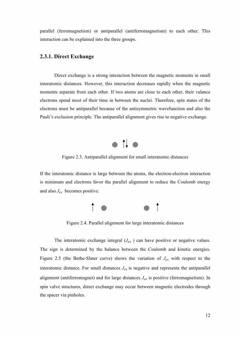
Figure 2.3. Antiparallel alignment for small interatomic distances
If the interatomic distance is large between the atoms, the electron-electron interaction
is minimum and electrons favor the parallel alignment to reduce the Coulomb energy
and also Jex becomes positive.
Figure 2.4. Parallel alignment for large interatomic distances
The interatomic exchange integral (Jex ) can have positive or negative values.
The sign is determined by the balance between the Coulomb and kinetic energies.
Figure 2.5 (the Bethe-Slater curve) shows the variation of Jex with respect to the
interatomic distance. For small distances Jex is negative and represents the antiparallel
alignment (antiferromagnet) and for large distances Jex is positive (ferromagnetism). In
spin valve structures, direct exchange may occur between magnetic electrodes through
the spacer via pinholes.

13
Jex
Interatomic distance
Figure.2.5. The Bethe-Slater curve
2.3.2. Indirect Exchange
This type of interaction causes the coupling of atomic magnetic dipole moments
at large distances and is known as RKKY (Ruderman-Kittel-Kasuya-Yosida)
interaction. It is generally seen in metals and occurs via the conduction electrons. A
magnetic ion polarizes the conduction electrons around it via the exchange interaction
and these polarized conduction electrons are sensed by another magnetic ion at a certain
distance. The form of coupling is -2JexSiSj, where Jex oscillates from positive sign to
negative and its magnitude damps with the increasing distance between magnetic ions.
Depending of the sign of Jex, interaction can be ferromagnetic or antiferromagnetic. The
variation of exchange integral versus interatomic distance is shown in the Figure 2.6.
This type of interaction may occur in spin valve structures when the thickness of the
spacer layer is bigger than a few nanometer.
Figure 2.6. Indirect exchange versus the interatomic distance
Ni
Co
Fe
Mn Interatomic distance
Jex
14
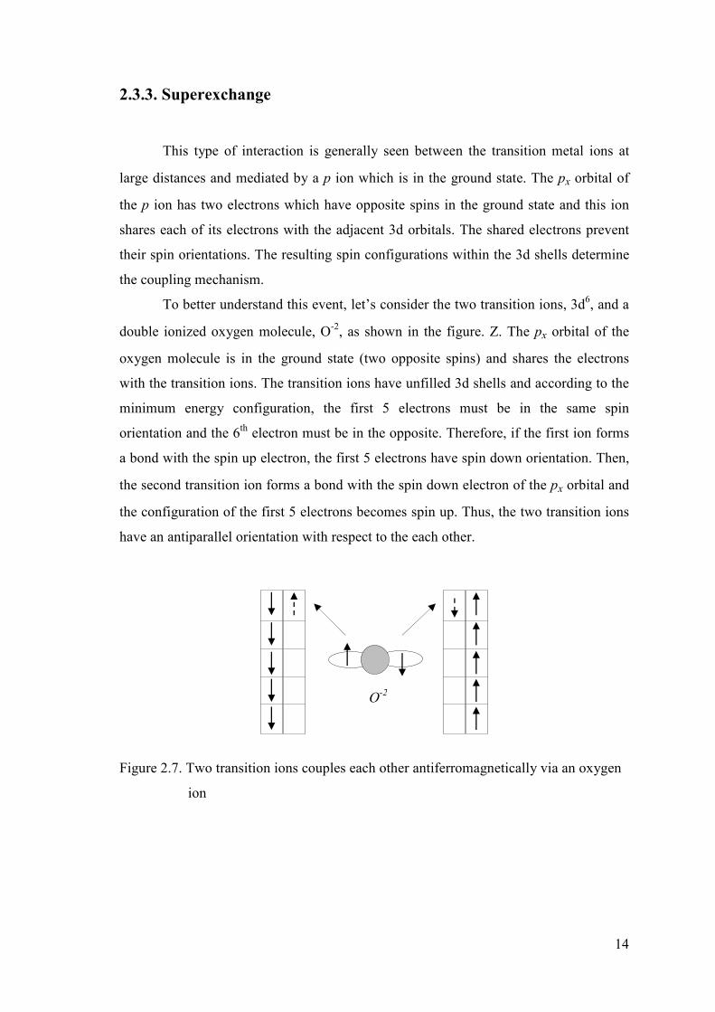
2.3.3. Superexchange
This type of interaction is generally seen between the transition metal ions at
large distances and mediated by a p ion which is in the ground state. The px orbital of
the p ion has two electrons which have opposite spins in the ground state and this ion
shares each of its electrons with the adjacent 3d orbitals. The shared electrons prevent
their spin orientations. The resulting spin configurations within the 3d shells determine
the coupling mechanism.
To better understand this event, let’s consider the two transition ions, 3d6, and a
double ionized oxygen molecule, O-2, as shown in the figure. Z. The px orbital of the
oxygen molecule is in the ground state (two opposite spins) and shares the electrons
with the transition ions. The transition ions have unfilled 3d shells and according to the
minimum energy configuration, the first 5 electrons must be in the same spin
orientation and the 6th electron must be in the opposite. Therefore, if the first ion forms
a bond with the spin up electron, the first 5 electrons have spin down orientation. Then,
the second transition ion forms a bond with the spin down electron of the px orbital and
the configuration of the first 5 electrons becomes spin up. Thus, the two transition ions
have an antiparallel orientation with respect to the each other.
Figure 2.7. Two transition ions couples each other antiferromagnetically via an oxygen
ion
O-2
15
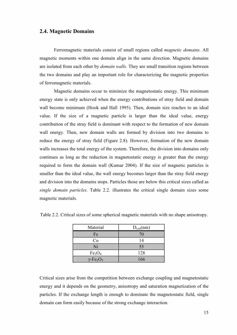
2.4. Magnetic Domains
Ferromagnetic materials consist of small regions called magnetic domains. All
magnetic moments within one domain align in the same direction. Magnetic domains
are isolated from each other by domain walls. They are small transition regions between
the two domains and play an important role for characterizing the magnetic properties
of ferromagnetic materials.
Magnetic domains occur to minimize the magnetostatic energy. This minimum
energy state is only achieved when the energy contributions of stray field and domain
wall become minimum (Hook and Hall 1995). Then, domain size reaches to an ideal
value. If the size of a magnetic particle is larger than the ideal value, energy
contribution of the stray field is dominant with respect to the formation of new domain
wall energy. Then, new domain walls are formed by division into two domains to
reduce the energy of stray field (Figure 2.8). However, formation of the new domain
walls increases the total energy of the system. Therefore, the division into domains only
continues as long as the reduction in magnetostatic energy is greater than the energy
required to form the domain wall (Kumar 2004). If the size of magnetic particles is
smaller than the ideal value, the wall energy becomes larger than the stray field energy
and division into the domains stops. Particles those are below this critical sizes called as
single domain particles. Table 2.2. illustrates the critical single domain sizes some
magnetic materials.
Table 2.2. Critical sizes of some spherical magnetic materials with no shape anisotropy.
Critical sizes arise from the competition between exchange coupling and magnetostatic
energy and it depends on the geometry, anisotropy and saturation magnetization of the
particles. If the exchange length is enough to dominate the magnetostatic field, single
domain can form easily because of the strong exchange interaction.
Material Dcrit(nm)
Fe 70 Co 14 Ni 55 Fe3O4 128 γ-Fe2O3 166
16
Figure 2.8. Formation of new domains causes decreasing of the energy within the stray
field
As it is defined above, all magnetic moments align at a certain direction within
one domain in the absence of an external field. This preferred direction called as easy
axes and its orientation is in the different directions for the different domains.
2.5. Magnetic Anisotropy
Magnetic anisotropy is one of the most significant factors in order to
characterize the magnetic materials and it may strongly affect the shape of the magnetic
hysteresis loop. The simple explanation of anisotropy is that magnetic properties of a
magnetic sample depend on the direction they are measured. The most important types
of magnetic anisotropies are magnetocrystalline, shape and exchange anisotropies.
2.5.1. Magnetocrystalline anisotropy
Magnetocrystalline anisotropy can be thought as a force to keep the orientation
of magnetic moments in a certain direction. Magnetic moments generally prefer to align
along one direction of a crystalline cubic structure as an easy axis. Easy axis results
from the spin-orbit coupling between the spin and orbital motion of an electron and less
field require magnetizing the sample at that direction. The orbital motion of an electron
is strongly affected by the lattice point (crystal field). Then, this effect is seen on the
spin angular momentum of the electrons because of the spin-orbit coupling. Therefore,
there is a correlation between the crystal field, orbital angular momentum and spin
angular momentum of an electron. When an external force tries to rotate the spin of one
17
electron, the orbit of that electron also tends to rotate. However, orbital motion fixed by
crystal field blocks the reorientation of spin axis. Thus, magnetic dipole moment of the
electron aligns along a preferred direction under these interactions. The energy required
to overcome the spin-orbit coupling and rotate the spins away from the easy axes is
called as anisotropy energy. Quantitative measurement of magnetocrystalline
anisotropy field, Ha, can be determined by saturating the sample in the hard axes in
which the field required to magnetize the sample to saturation is largest. Figure 2.9.
shows the relative crystallographic directions for easy and hard axis of hcp cobalt
structure and their magnetization curves.
Figure 2.9. a) Crystallographic hcp structure of cobalt and b) easy and hard direction
magnetization curves
The c axis is defined as magnetocrystalline easy axis and any direction in the basal
plane is defined as hard axis. The stored energy difference between the easy and hard
axis is the magnetocrystalline anisotropy energy (Ea) and it is expressed as following
formula;
Ea = K0+K1Sin2θ+K2Sin
4θ+...
a
[0001]
[1010]
Ms
b
[0001]
Ha H
M
[1010]]
18
where Ki is the energy density and θ is the angle between magnetization vector and
easy axis. However, for symmetric cubic crystals, the anisotropy energy is calculated by
using the direction cosines of the magnetization with respect to the crystal axes and is
defined as
Ea = K0+K1(
where αi = Cos θi is the angle between magnetization and i
th axis.
2.5.2 Shape Anisotropy
The shape anisotropy depends on the dimensions of magnetic materials and
results from the demagnetizing factor. A magnetized sample produces magnetic poles
on the surface and these poles create another magnetic source called as demagnetizing
field (Hd). The demagnetizing field lies in the opposite direction of the field forming it.
Then, the net field (Hi) inside the specimen becomes
Hi = H - Hd
where Hd is the demagnetizing field. The demagnetizing field is proportional to the
magnetization and the proportionality constant is described as demagnetizing factor, Hd
= NdM. Nd depends on the geometry of the specimen. In order to understand the effect
of demagnetizing field on the shape anisotropy, a needle type specimen can be useful.
When an external field magnetizes the specimen in Figure 2.10, the demagnetizing field
along the long axis is less than along the short axis. Then, the long axis behaves as an
easy axis. However, this situation can not be seen in the spherical samples because they
have no shape anisotropy.

19
Figure 2.10. The demagnetizing field produced by surface pole distribution
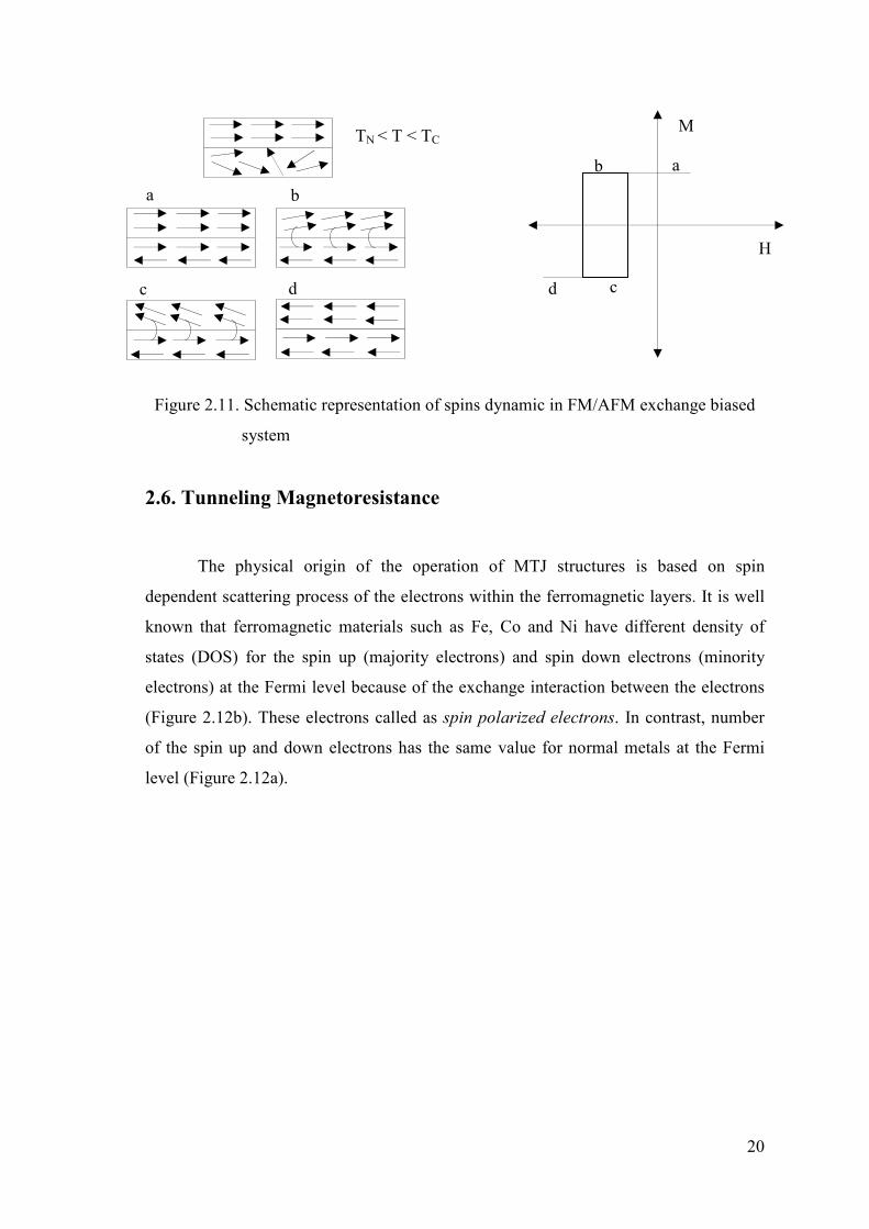
2.5.3 Exchange Anisotropy
Exchange anisotropy (exchange bias) is one of the most important types of
anisotropy used in many technological applications such as magnetoresistive devices. It
was discovered by Meiklejohn and Bean (1957) and it results from an interaction
between ferromagnetic and antiferromagnetic layers. When a FM/AFM system is
cooled down below the Neel temperature, which is a specific temperature for transition
between antiferromagnetic and paramagnetic phases for antiferromagnets, under an
external field the spins of the second layer become antiferromagnetically ordered and
they exert a torque on the spins of the FM layer to keep them their original direction. It
is difficult to rotate the direction of an antiferromagnet with respect to a ferromagnet.
Because of the torque, ferromagnetic layer can not be rotated easily with the external
field in the FM/AFM system but it is easy to rotate if the external field is in the original
magnetization direction of the ferromagnetic layer. These two effects cause a shift in
the hysteresis loop on the field axis. Figure 2.11 shows the anisotropy process
schematically.
Hd
s s
s s
n
n
n
n
H
M
20
Figure 2.11. Schematic representation of spins dynamic in FM/AFM exchange biased
system
2.6. Tunneling Magnetoresistance
The physical origin of the operation of MTJ structures is based on spin
dependent scattering process of the electrons within the ferromagnetic layers. It is well
known that ferromagnetic materials such as Fe, Co and Ni have different density of
states (DOS) for the spin up (majority electrons) and spin down electrons (minority
electrons) at the Fermi level because of the exchange interaction between the electrons
(Figure 2.12b). These electrons called as spin polarized electrons. In contrast, number
of the spin up and down electrons has the same value for normal metals at the Fermi
level (Figure 2.12a).
d c
a b
b a
c d
H
M TN < T < TC
21
Figure 2.12. Schematic representation of DOS a) for a normal metal and b) for a
ferromagnetic metal (arrows show majority and minority spin states)
The different DOSs lead to specific transport behavior of the majority and
minority spin electrons in a FM material (Mott 1936). If the two FM layers have
different DOS at the Fermi level, the polarized electrons which are located at the high
energy levels in one electrode starts to move to the other electrode which has lower
energy states at the Fermi level in order to achieve minimum energy configuration.
When the electrons reach to the other FM layer, spin dependent scattering may occur
due to the polarization of DOS of that layer. The Figure 2.13 shows the spin dependent
scattering in a FM. The same things can be thought for GMR structures. During the
same process there is no any spin dependent scattering within the nonmagnetic spacer
layer because there are a lot of empty energy states for spin up and down electrons.
Furthermore, number of these states is equal so spacer layer does not act as a restrictive
layer on the electron motion.
E E
EF
Density of state
a b
22
Ψ(x)
Figure 2.13. The DOS of two antiparallel ferromagnets and spin dependent scattering
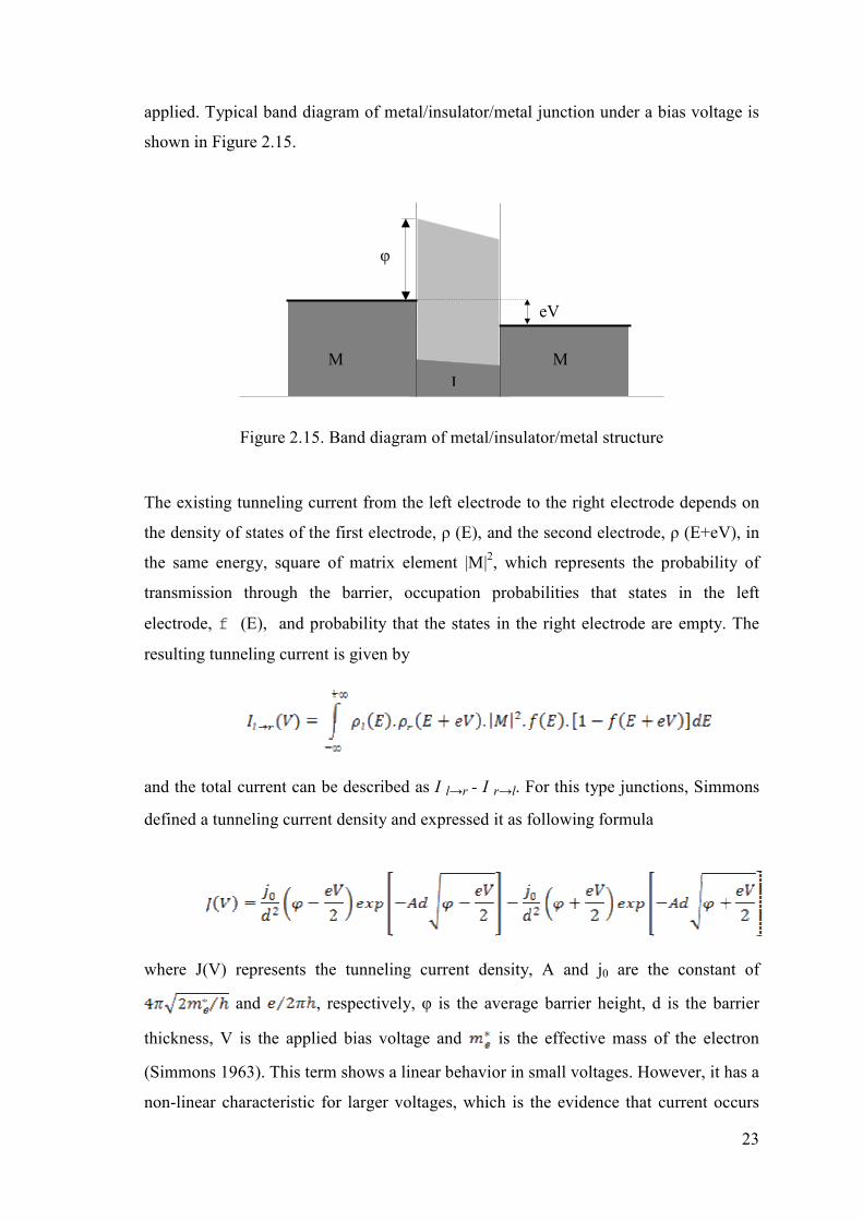
The transport mechanism of the electrons within the insulating layer is the
tunneling phenomenon which is a quantum mechanical effect. Electrons have both
particle and wave like properties. Tunneling is a wave like effect of electrons. When
electrons come across an energy barrier, their wave functions do not end abruptly and
can pass through the barrier although the energies of electrons are less than the energy
barrier. Then, same electrons can appear on the other side of the barrier. However, this
effect can not be classically observed. The Figure 2.14 shows the tunneling effect.
Figure 2.14. Wave function exponentially decays within the energy barrier
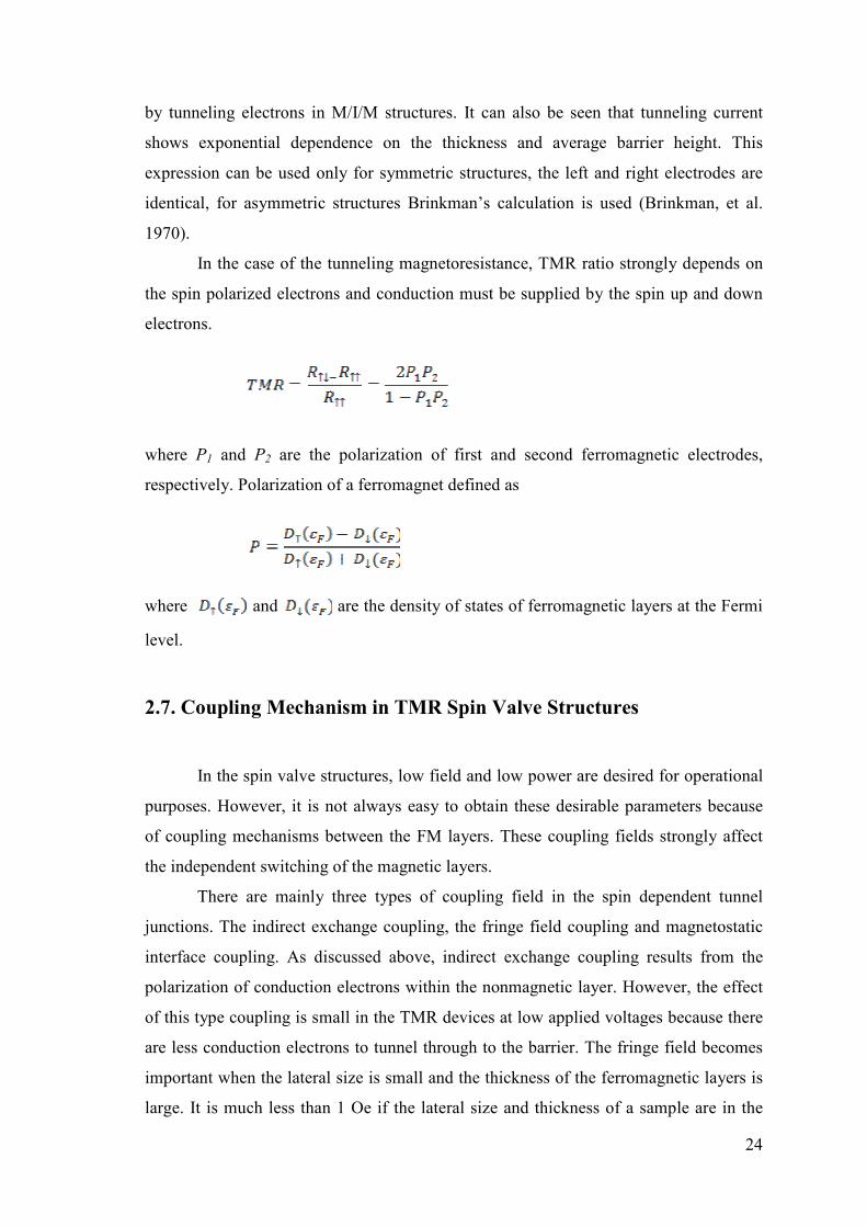
In magnetic tunnel junctions, electrons tunnel from one electrode to the other
electrode and there exists a tunnel current if the electrodes have different Fermi energy.
In order to create a potential difference between the electrodes a bias voltage (eV) is
a
Density of state
b
E E
EF
23
applied. Typical band diagram of metal/insulator/metal junction under a bias voltage is
shown in Figure 2.15.
Figure 2.15. Band diagram of metal/insulator/metal structure
The existing tunneling current from the left electrode to the right electrode depends on
the density of states of the first electrode, ρ (E), and the second electrode, ρ (E+eV), in
the same energy, square of matrix element |M|2, which represents the probability of
transmission through the barrier, occupation probabilities that states in the left
electrode, f (E), and probability that the states in the right electrode are empty. The
resulting tunneling current is given by
and the total current can be described as I l→r - I r→l. For this type junctions, Simmons
defined a tunneling current density and expressed it as following formula
where J(V) represents the tunneling current density, A and j0 are the constant of
and , respectively, φ is the average barrier height, d is the barrier
thickness, V is the applied bias voltage and is the effective mass of the electron
(Simmons 1963). This term shows a linear behavior in small voltages. However, it has a
non-linear characteristic for larger voltages, which is the evidence that current occurs
φ
eV
M M I
24
by tunneling electrons in M/I/M structures. It can also be seen that tunneling current
shows exponential dependence on the thickness and average barrier height. This
expression can be used only for symmetric structures, the left and right electrodes are
identical, for asymmetric structures Brinkman’s calculation is used (Brinkman, et al.
1970).
In the case of the tunneling magnetoresistance, TMR ratio strongly depends on
the spin polarized electrons and conduction must be supplied by the spin up and down
electrons.
where P1 and P2 are the polarization of first and second ferromagnetic electrodes,
respectively. Polarization of a ferromagnet defined as
where and are the density of states of ferromagnetic layers at the Fermi
level.
2.7. Coupling Mechanism in TMR Spin Valve Structures
In the spin valve structures, low field and low power are desired for operational
purposes. However, it is not always easy to obtain these desirable parameters because
of coupling mechanisms between the FM layers. These coupling fields strongly affect
the independent switching of the magnetic layers.
There are mainly three types of coupling field in the spin dependent tunnel
junctions. The indirect exchange coupling, the fringe field coupling and magnetostatic
interface coupling. As discussed above, indirect exchange coupling results from the
polarization of conduction electrons within the nonmagnetic layer. However, the effect
of this type coupling is small in the TMR devices at low applied voltages because there
are less conduction electrons to tunnel through to the barrier. The fringe field becomes
important when the lateral size is small and the thickness of the ferromagnetic layers is
large. It is much less than 1 Oe if the lateral size and thickness of a sample are in the

25
order of mm and 10 nm, respectively (Wang, et al. 2000). Therefore, only the effect of
interface coupling field is responsible for the coupling mechanism between the FM
layers in these large samples. The interface coupling includes pinholes coupling, Neel
wall coupling and Neel coupling (orange-peel coupling).
2.7.1. Pinhole Coupling
The pinhole coupling occurs when the thickness of the barrier layer is very thin.
The direct interaction is responsible for this type coupling. When the barrier thickness is
very thin, small pinholes can exist during the deposition process of the barrier and they
act as a conduction bridge. Then, two FM layers contact with each other via the
conduction bridges through the nonmagnetic (NM) layer. If the NM layer is an insulator
instead of a conducting metal, pinhole coupling can be easily determined from I-V
characteristic. Pinholes cause a shortcut between the magnetic layers and linear
conduction is seen rather than tunneling. Figure 2.16 represents the pinhole coupling.
Figure 2.16. Small pinholes inside the encircled regions causes the coupling through the
very thin nonmagnetic layer.
2.7.2. Neel Coupling (Orange-peel Coupling)
The Neel coupling is a roughness dependent coupling and tends to be parallel
alignment of the magnetic layers. During the deposition process of the fixed magnetic
layer, a sinusoidal surface roughness can exist and magnetic poles occur on the bumps.
These poles create magnetic stray fields and they are sensed by the second magnetic
layer. Then, ferromagnetic coupling exist between the two magnetic layers. If the
magnetizations of two layers are parallel, magnetostatic charges of opposite signs
appear symmetrically. In contrast, if the magnetizations are antiparallel, charges of the
FM NM FM

26
tF tS
M
HN λ
h
FM NM FM
same signs are facing each other leading to an increase in energy. This causes an
effective FM coupling which has low energy between the two magnetic layers. As the
barrier thickness increases, coupling field strength decreases exponentially. The field
strength is given by the following equation,
where h and λ are the amplitude and wavelength of the roughness, tF and tS are the
thickness of the free and barrier layer, Ms is the saturation magnetization of the free
layer. Figure 2.17 represents the roughness induced stray fields between two FM layers
separated by a NM layer.
Figure 2.17. The roughness induced Neel coupling
2.5.3. Neel Wall Coupling
This type of coupling arises from the domain wall stray fields. Spin orientation
changes from 0° to 180° within a Neel type domain wall and magnetic pole density
occurs at the domain boundaries. This pole density creates magnetic stray fields which
can exert a force on the adjacent magnetic layer. Domain wall motion of a single layer
effects the other neighboring domain wall and the two layer switches together. In a
multilayer structure, domain wall coupling makes the Hc of the whole layer smaller
than that of a single layer. For spin valve structures, the effect of this coupling can be
eliminated by creating the two different coercivities for magnetic layers. The Figure
2.18 shows the induced stray field of a Neel type domain wall and coupling mechanism.

27
Figure 2.18. a) Induced stray field on domain boundaries and b)Neel wall coupling
between the two magnetic layers. The spin orientations inside the walls
tend to be opposite in order to reduce dipole-dipole interaction energy
for each domains (Wang, et al. 2000)
FM
NM
FM
a b
+ +
28
CHAPTER 3
MATERIAL PROPERTIES
In this chapter, structural and magnetic properties of Fe, Co, Ta, and Ta2O5 will
be discussed. These materials have been used for producing the MTJ structures in this
thesis.
3.1. Iron (Fe)
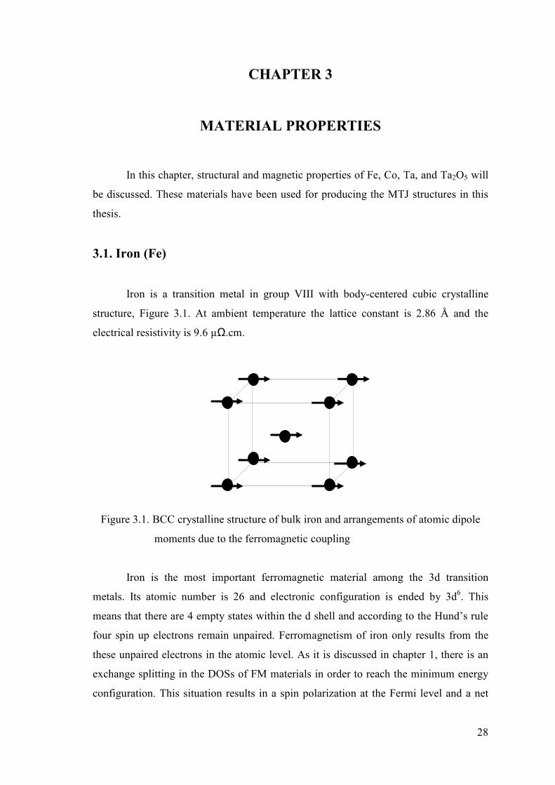
Iron is a transition metal in group VIII with body-centered cubic crystalline
structure, Figure 3.1. At ambient temperature the lattice constant is 2.86 Å and the
electrical resistivity is 9.6 µΩ.cm.
Figure 3.1. BCC crystalline structure of bulk iron and arrangements of atomic dipole
moments due to the ferromagnetic coupling
Iron is the most important ferromagnetic material among the 3d transition
metals. Its atomic number is 26 and electronic configuration is ended by 3d6. This
means that there are 4 empty states within the d shell and according to the Hund’s rule
four spin up electrons remain unpaired. Ferromagnetism of iron only results from the
these unpaired electrons in the atomic level. As it is discussed in chapter 1, there is an
exchange splitting in the DOSs of FM materials in order to reach the minimum energy
configuration. This situation results in a spin polarization at the Fermi level and a net
29
magnetic dipole moment is created. For iron the net magnetic moment is 2.2 µB and
magnetization value (bulk) is 1714 emu/cm3. Its coercive field is around 20 Gauss and
the Curie temperature of iron is 1043 K.
3.2. Cobalt (Co)
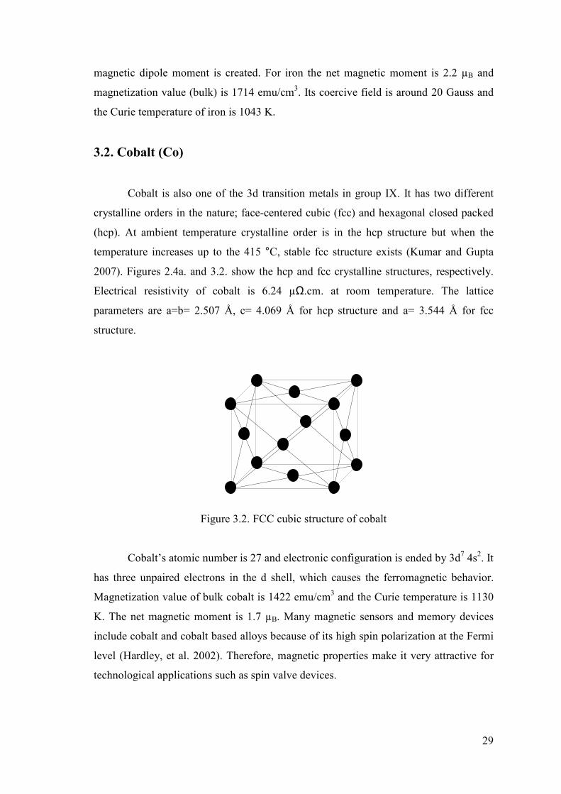
Cobalt is also one of the 3d transition metals in group IX. It has two different
crystalline orders in the nature; face-centered cubic (fcc) and hexagonal closed packed
(hcp). At ambient temperature crystalline order is in the hcp structure but when the
temperature increases up to the 415 °C, stable fcc structure exists (Kumar and Gupta
2007). Figures 2.4a. and 3.2. show the hcp and fcc crystalline structures, respectively.
Electrical resistivity of cobalt is 6.24 µΩ.cm. at room temperature. The lattice
parameters are a=b= 2.507 Å, c= 4.069 Å for hcp structure and a= 3.544 Å for fcc
structure.
Figure 3.2. FCC cubic structure of cobalt
Cobalt’s atomic number is 27 and electronic configuration is ended by 3d7 4s2. It
has three unpaired electrons in the d shell, which causes the ferromagnetic behavior.
Magnetization value of bulk cobalt is 1422 emu/cm3 and the Curie temperature is 1130
K. The net magnetic moment is 1.7 µB. Many magnetic sensors and memory devices
include cobalt and cobalt based alloys because of its high spin polarization at the Fermi
level (Hardley, et al. 2002). Therefore, magnetic properties make it very attractive for
technological applications such as spin valve devices.
30
3.3. Tantalum (Ta) and Tantalum Oxide (TaOx)
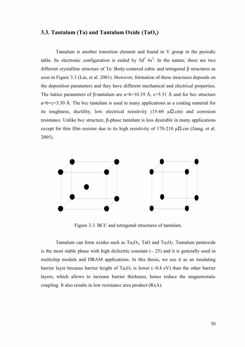
Tantalum is another transition element and found in V group in the periodic
table. Its electronic configuration is ended by 5d3 6s2. In the nature, there are two
different crystalline structure of Ta: Body-centered cubic and tetragonal β structures as
seen in Figure 3.3 (Liu, et al. 2001). However, formation of these structures depends on
the deposition parameters and they have different mechanical and electrical properties.
The lattice parameters of β-tantalum are a=b=10.19 Å, c=5.31 Å and for bcc structure
a=b=c=3.30 Å. The bcc tantalum is used in many applications as a coating material for
its toughness, ductility, low electrical resistivity (15-60 µΩ.cm) and corrosion
resistance. Unlike bcc structure, β-phase tantalum is less desirable in many applications
except for thin film resistor due to its high resistivity of 170-210 µΩ.cm (Jiang, et al.
2005).
Figure 3.3. BCC and tetragonal structures of tantalum.
Tantalum can form oxides such as Ta2O3, TaO and Ta2O5. Tantalum pentoxide
is the most stable phase with high dielectric constant (~ 25) and it is generally used in
multichip module and DRAM applications. In this thesis, we use it as an insulating
barrier layer because barrier height of Ta2O5 is lower (~0.4 eV) than the other barrier
layers, which allows to increase barrier thickness, hence reduce the magnetostatic
coupling. It also results in low resistance area product (RxA).

31
CHAPTER 4
EXPERIMENTAL TECHNIQUES
In this chapter, the growth and characterization techniques will be discussed. All
the layers were grown in a UHV magnetron sputtering system. The structural properties
were studied by X-ray powder diffraction (XRD), and atomic force microscopy (AFM).
Magnetic properties were studied by vibrating sample magnetometer (VSM).
Ellipsometry was used to study the properties of the TaOx insulator layer. Electrical and
magnetoresistance measurements were performed by four point probe technique.
4.1. Magnetron Sputtering System
Sputtering technique is one of the most commonly used methods for thin film
deposition. When a solid surface is bombarded by energetic particles such as ions, it is
seen that surface atoms of the solid are removed from the surface because of the
collision between the ions and the surface atoms. This phenomenon is known as
sputtering. In a sputtering system, a potential difference is created between the target
and substrate and the target is hold generally in the negative voltage. Then, the ionized
Ar gases (Ar+) are accelerated towards the target under an electric field. After that, Ar+
ions transfer their kinetic energies to the surface atom by collision and the surface
atoms ejected from the target and stick on the substrate surface, resulting in growth of
films. In the magnetron sputtering system, magnets are placed under the target in order
to trap the electrons created in the sputtering process and to increase the ionizing
probability. The Figure 4.1 shows the schematic magnetic configuration of a magnetron
head.
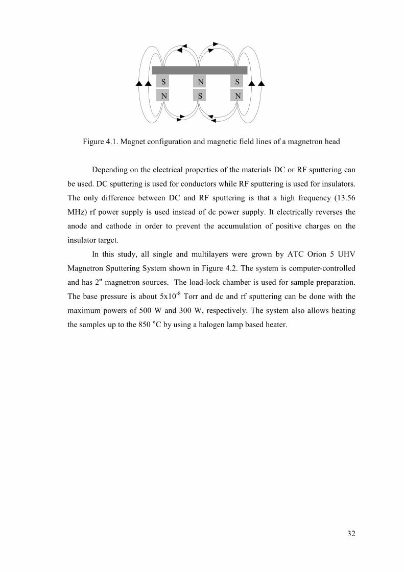
32
S
N
S
N S
N
Figure 4.1. Magnet configuration and magnetic field lines of a magnetron head
Depending on the electrical properties of the materials DC or RF sputtering can
be used. DC sputtering is used for conductors while RF sputtering is used for insulators.
The only difference between DC and RF sputtering is that a high frequency (13.56
MHz) rf power supply is used instead of dc power supply. It electrically reverses the
anode and cathode in order to prevent the accumulation of positive charges on the
insulator target.
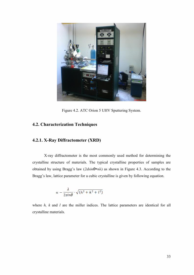
In this study, all single and multilayers were grown by ATC Orion 5 UHV
Magnetron Sputtering System shown in Figure 4.2. The system is computer-controlled
and has 2'' magnetron sources. The load-lock chamber is used for sample preparation.
The base pressure is about 5x10⁻⁸ Torr and dc and rf sputtering can be done with the
maximum powers of 500 W and 300 W, respectively. The system also allows heating
the samples up to the 850 °C by using a halogen lamp based heater.
33
Figure 4.2. ATC Orion 5 UHV Sputtering System.
4.2. Characterization Techniques
4.2.1. X-Ray Diffractometer (XRD)
X-ray diffractometer is the most commonly used method for determining the
crystalline structure of materials. The typical crystalline properties of samples are
obtained by using Bragg’s law (2dsinθ=nλ) as shown in Figure 4.3. According to the
Bragg’s law, lattice parameter for a cubic crystalline is given by following equation.
where h, k and l are the miller indices. The lattice parameters are identical for all
crystalline materials.
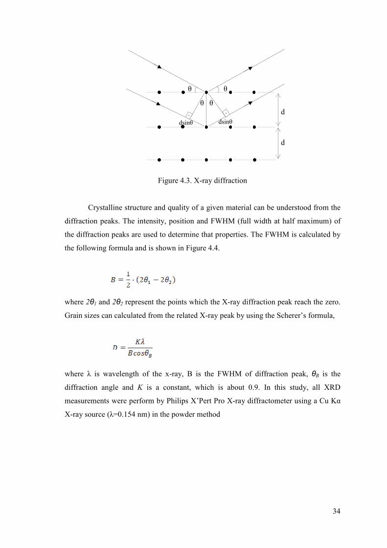
34
Figure 4.3. X-ray diffraction
Crystalline structure and quality of a given material can be understood from the
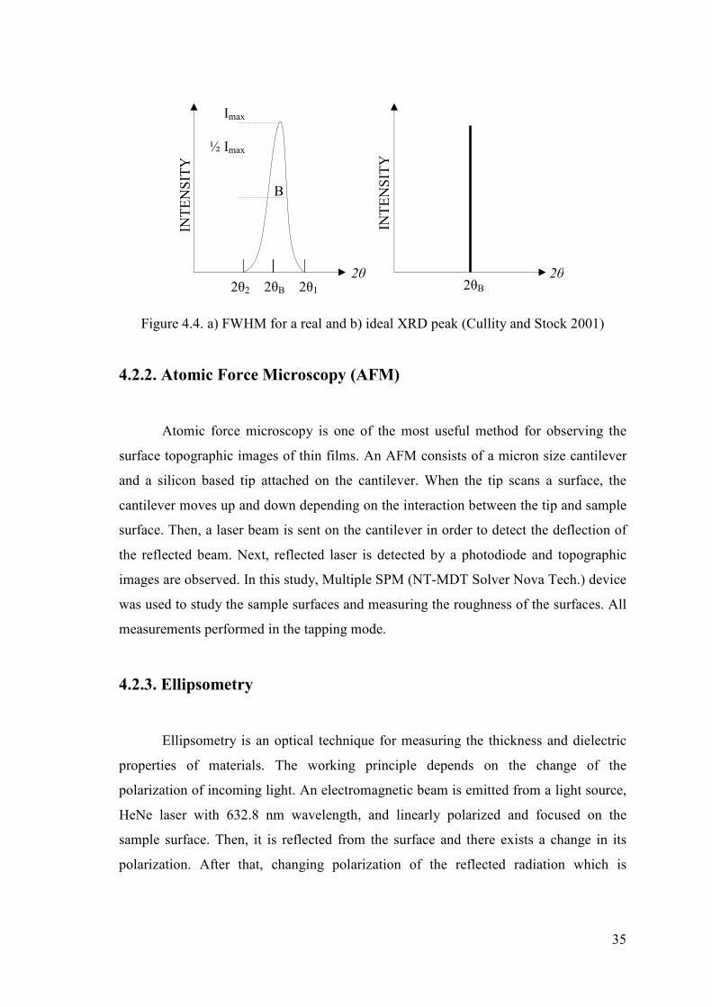
diffraction peaks. The intensity, position and FWHM (full width at half maximum) of
the diffraction peaks are used to determine that properties. The FWHM is calculated by
the following formula and is shown in Figure 4.4.
where 2θ1 and 2θ2 represent the points which the X-ray diffraction peak reach the zero.
Grain sizes can calculated from the related X-ray peak by using the Scherer’s formula,
where λ is wavelength of the x-ray, B is the FWHM of diffraction peak, θB is the
diffraction angle and K is a constant, which is about 0.9. In this study, all XRD
measurements were perform by Philips X’Pert Pro X-ray diffractometer using a Cu Kα
X-ray source (λ=0.154 nm) in the powder method
d
d dsinθ dsinθ
θ θ
θ θ
35
2θB 2θ
B
Imax ½ Imax
2θ 2θ2 2θB 2θ1
INTENSITY
INTENSITY
Figure 4.4. a) FWHM for a real and b) ideal XRD peak (Cullity and Stock 2001)
4.2.2. Atomic Force Microscopy (AFM)
Atomic force microscopy is one of the most useful method for observing the
surface topographic images of thin films. An AFM consists of a micron size cantilever
and a silicon based tip attached on the cantilever. When the tip scans a surface, the
cantilever moves up and down depending on the interaction between the tip and sample
surface. Then, a laser beam is sent on the cantilever in order to detect the deflection of
the reflected beam. Next, reflected laser is detected by a photodiode and topographic
images are observed. In this study, Multiple SPM (NT-MDT Solver Nova Tech.) device
was used to study the sample surfaces and measuring the roughness of the surfaces. All
measurements performed in the tapping mode.
4.2.3. Ellipsometry
Ellipsometry is an optical technique for measuring the thickness and dielectric
properties of materials. The working principle depends on the change of the
polarization of incoming light. An electromagnetic beam is emitted from a light source,
HeNe laser with 632.8 nm wavelength, and linearly polarized and focused on the
sample surface. Then, it is reflected from the surface and there exists a change in its
polarization. After that, changing polarization of the reflected radiation which is
36
proportional to the sample properties such as thickness and refractive index is measured
by a detector. This method is useful for thin film experiments.
In this study, we used Sentech SE801-E spectroscopic ellipsometry only to
measure the refractive index of TaOx insulating layer.
4.2.4. Vibrating Sample Magnetometer (VSM)
Vibrating sample magnetometer is used to measure the magnetic properties of
magnetic samples. It consists of an electromagnet, a mechanically vibrating head and
sensing coils. The basic working principle depends on the Faraday’s law. When a
magnetic sample is placed within a uniform magnetic field, a magnetic moment, m, will
be induced in the sample. Then, the sample is forced to make a sinusoidal motion. Thus,
an induced voltage occurs in the sensing coils due to the changing magnetic flux. This
voltage is proportional to the magnetization of the sample. The induced voltage in the
sensing coils is given by,
where m is magnetic moment, A is amplitude of vibration, f is frequency of vibration
and S is sensitivity of sensing coils.
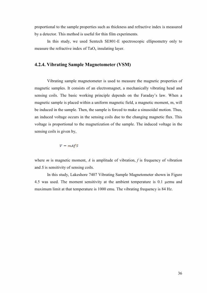
In this study, Lakeshore 7407 Vibrating Sample Magnetometer shown in Figure
4.5 was used. The moment sensitivity at the ambient temperature is 0.1 µemu and
maximum limit at that temperature is 1000 emu. The vibrating frequency is 84 Hz.
37
Figure 4.5. Lakeshore 7407 Vibrating Sample Magnetometer
4.2.5. Electrical and Magnetoresistance Measurements
Electrical measurements were done by conventional four-point probe technique.
A Keithley 2400 source meter and an I-V program written in labview were used for this
purpose. To connect the Keithley source meter to computer we also used Agilent
connection program for GPIB connection cable. After the connection between the
devices, electrical current was used as a source and voltage was sensed. Current was
increased from -1 µA to 1 µA and the step range was 10 nA. Figure 4.6 shows I-V
program used in this experiment.
To find the effective barrier height and thickness of the insulator the column of I
was divided by the area of junction and J-V curve was plotted. Then this curve was
fitted to the Simpson’s tunnel equation. Firstly, an arbitrary barrier height and thickness
were chosen and then curve fitted to the experimental data by changing the barrier
height and thickness.
38
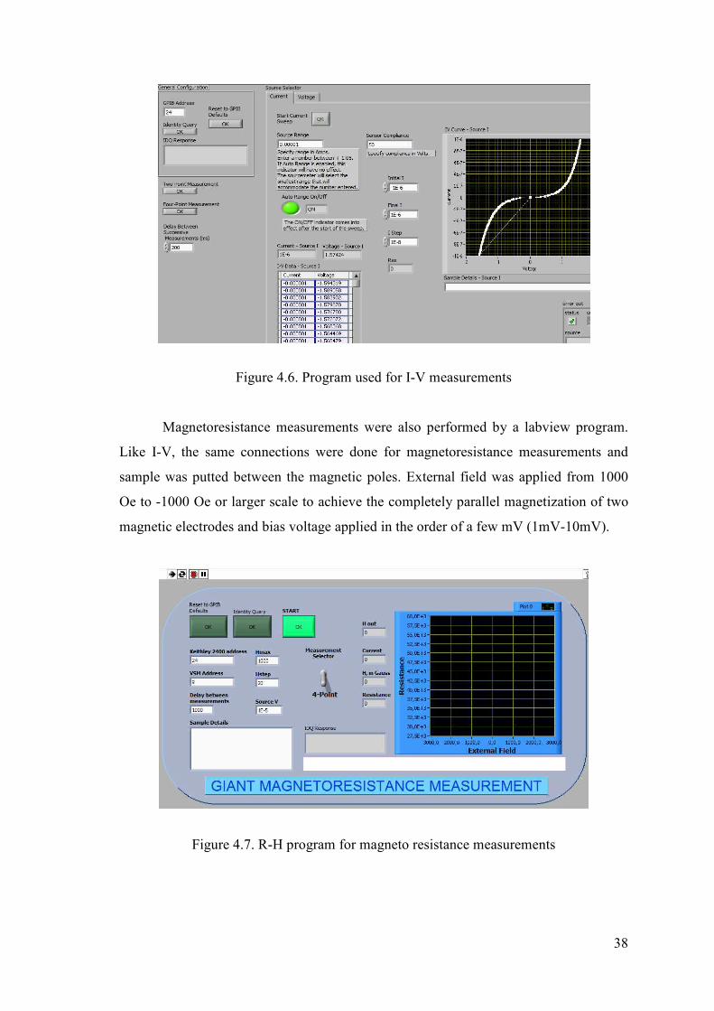
Figure 4.6. Program used for I-V measurements
Magnetoresistance measurements were also performed by a labview program.
Like I-V, the same connections were done for magnetoresistance measurements and
sample was putted between the magnetic poles. External field was applied from 1000
Oe to -1000 Oe or larger scale to achieve the completely parallel magnetization of two
magnetic electrodes and bias voltage applied in the order of a few mV (1mV-10mV).
Figure 4.7. R-H program for magneto resistance measurements

39
CHAPTER 5
RESULTS AND DISCUSSION
In this chapter, the relationships between magnetic and structural properties of
the magnetic multilayers and single layers will be discussed. It is well known that
magnetic properties of magnetic films strongly depend on the structural properties (Ng,
et al. 2002). Therefore, XRD and AFM analysis will be a key to understand the
magnetic behaviors.
5.1. X-Ray Diffraction Results
5.1.1. SiO2/Fe
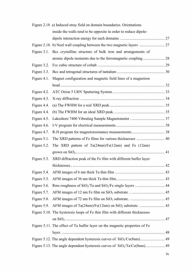
Figure 5.1 shows the XRD pattern of the various thickness of Fe grown on SiO2.
There is no visible peak for 6 nm Fe. However, when the thickness of the Fe layer
increases, the peak of Fe bcc (110) orientation appears at 2θ value of 44.96 degrees.
The intensity of this peak increases with increasing Fe thickness. The FWHM is 0.85°
and the corresponding grain size is 10.1 nm. When the thickness of the Fe film reaches
to 72 nm, the FWHM decreases to 0.53° and grain sizes increases to 16.1 nm. The XRD
data also show a shift in the Fe peak with increasing thickness. Calculated lattice
parameters are 2.851 Å and 2.865 Å for 12 and 72 nm Fe films, respectively. This
indicates the presence of a small strain in the thinner films, however the strain
disappears for the thicker film and lattice constant are close to the bulk Fe lattice
parameter.

40
30 35 40 45 50 55 60
0
200
400
600
800
1000
Inte
nsity
2θθθθ
X =6 nm
X =12 nm
X =24 nm
X =36 nm
X =72 nm
SiO2/ Fe(X)(110)
Figure 5.1. The XRD patterns of Fe films for various thicknesses
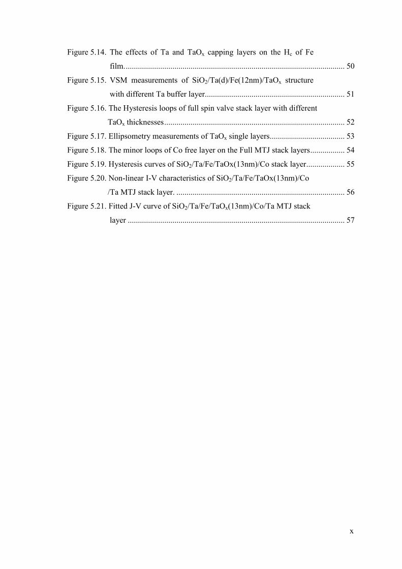
5.1.2. SiO2/Ta/Fe
In order to see the effect of Ta on the structure of Fe film, Ta buffer layer was
grown on the SiO2 substrate. Figure 5.2 shows the XRD pattern of 12 nm Fe grown on
24 nm Ta. There are two sharp peaks: bcc Fe (110) at 44.42°and β-Ta (200) at 33°.
When the Fe (110) peak is compared with the 12 nm Fe peak in the figure 5.1, it is seen
that Ta buffer layer increases the crystalline quality of Fe. The reason may relate to the
growing Fe on a crystalline Ta structure and hence it gains a crystalline order easily.
The calculated grain size and FWHM are 14.9 nm and 0.55°, respectively. Also the
calculated lattice parameter is 2.881 Å, which indicates the existence of a strain in the
Fe film. It can be inferred that the growth conditions and structure of buffer layer
strongly affect the structural properties of the magnetic thin films (Park, et al. 2002).
41
30 40 50 60
0
200
400
600
800
1000
1200
1400
Fe(110)
β−Τa(200)
2θθθθ
Inte
nsity
With Ta
W ithout Ta
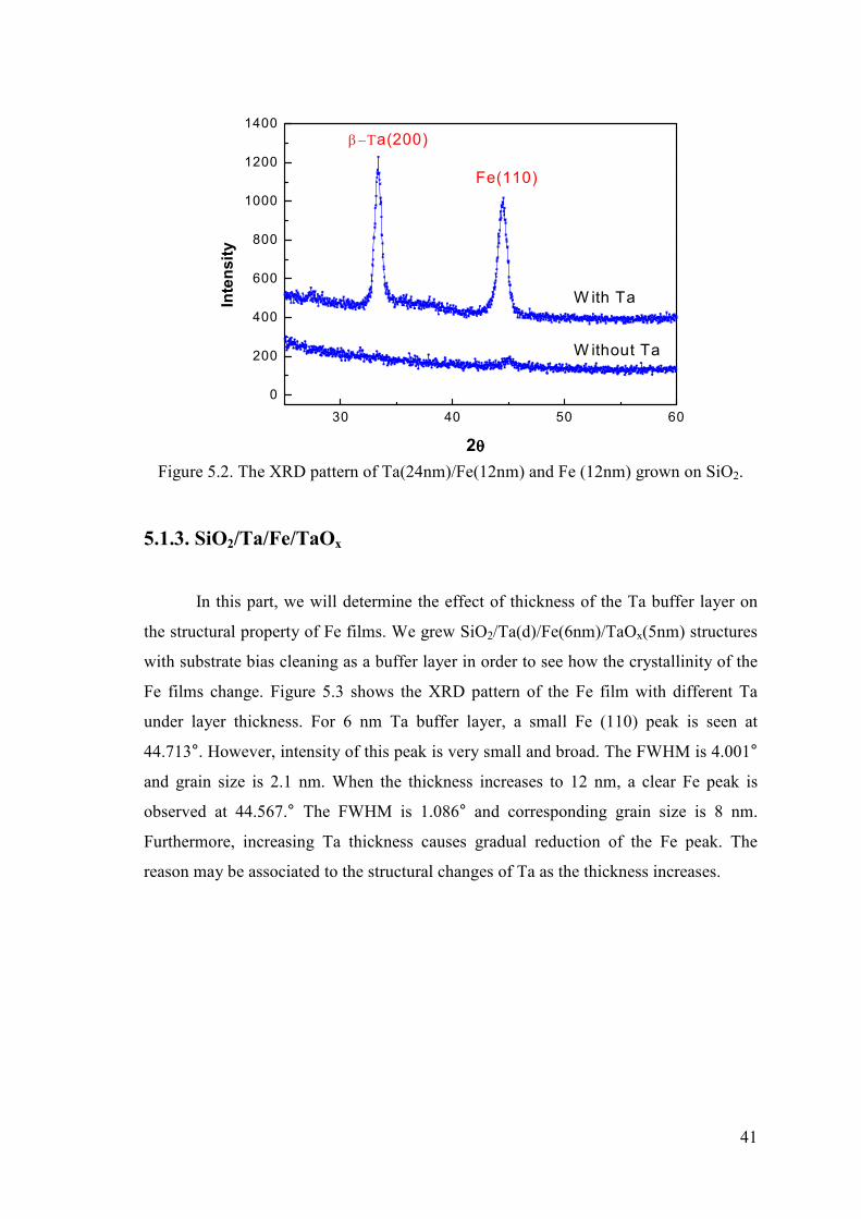
Figure 5.2. The XRD pattern of Ta(24nm)/Fe(12nm) and Fe (12nm) grown on SiO2.
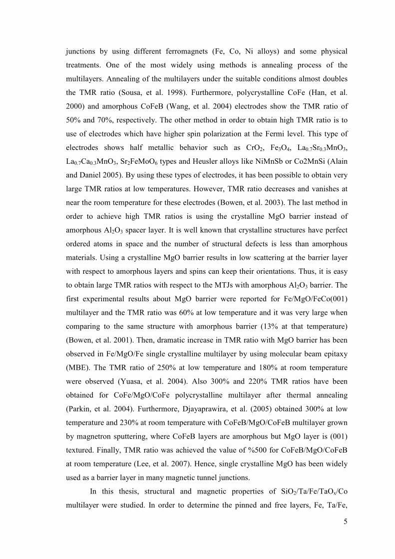
5.1.3. SiO2/Ta/Fe/TaOx
In this part, we will determine the effect of thickness of the Ta buffer layer on
the structural property of Fe films. We grew SiO2/Ta(d)/Fe(6nm)/TaOx(5nm) structures
with substrate bias cleaning as a buffer layer in order to see how the crystallinity of the
Fe films change. Figure 5.3 shows the XRD pattern of the Fe film with different Ta
under layer thickness. For 6 nm Ta buffer layer, a small Fe (110) peak is seen at
44.713°. However, intensity of this peak is very small and broad. The FWHM is 4.001°
and grain size is 2.1 nm. When the thickness increases to 12 nm, a clear Fe peak is
observed at 44.567.° The FWHM is 1.086° and corresponding grain size is 8 nm.
Furthermore, increasing Ta thickness causes gradual reduction of the Fe peak. The
reason may be associated to the structural changes of Ta as the thickness increases.

42
Figure 5.3. XRD pattern of Fe film with various buffer layer thicknesses.
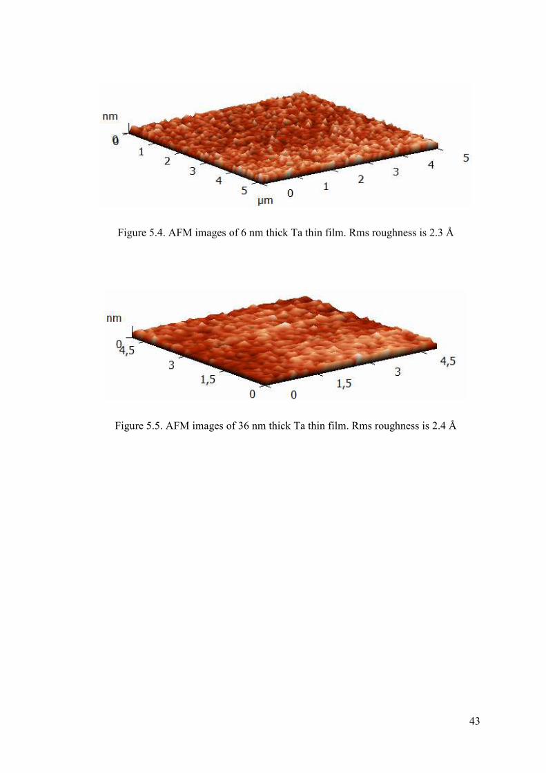
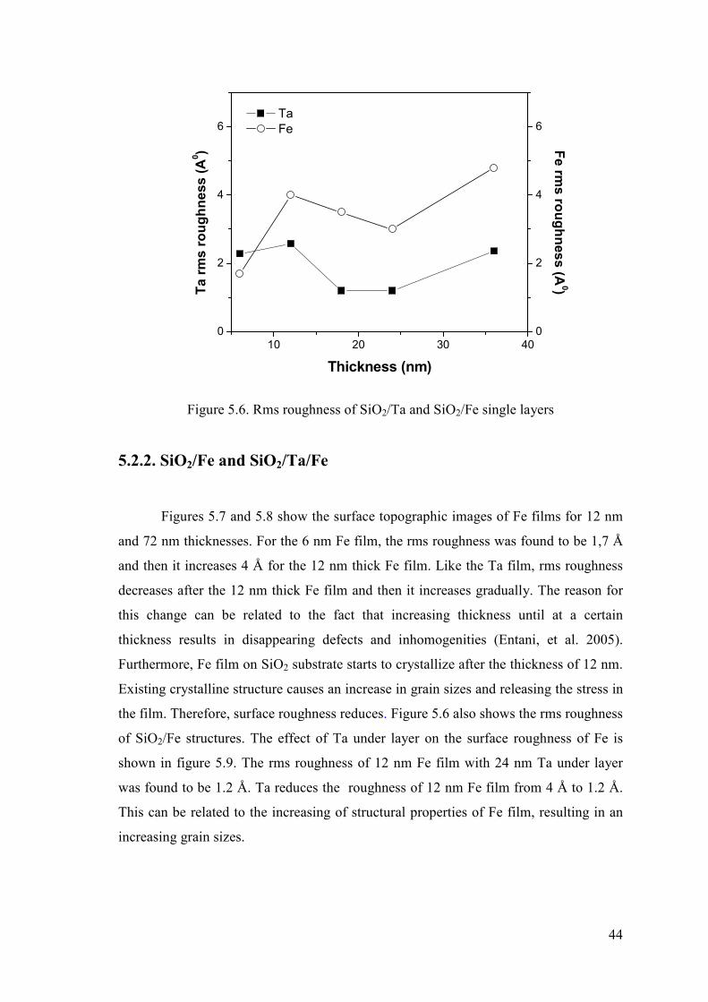
5.2. Atomic Force Microscopy Results
In order to observe the surface morphology and roughness analysis, which are
important parameters for magnetic interlayer coupling, 3D AFM images of Ta and Fe
layers were investigated. The scanned areas for all samples are 5x5 µm2. The surface
roughness of SiO2 substrate is 2 Å. It is atomically smooth. The roughness of the
substrate is important because it affects the over layer growth strongly.
5.2.1. SiO2/Ta
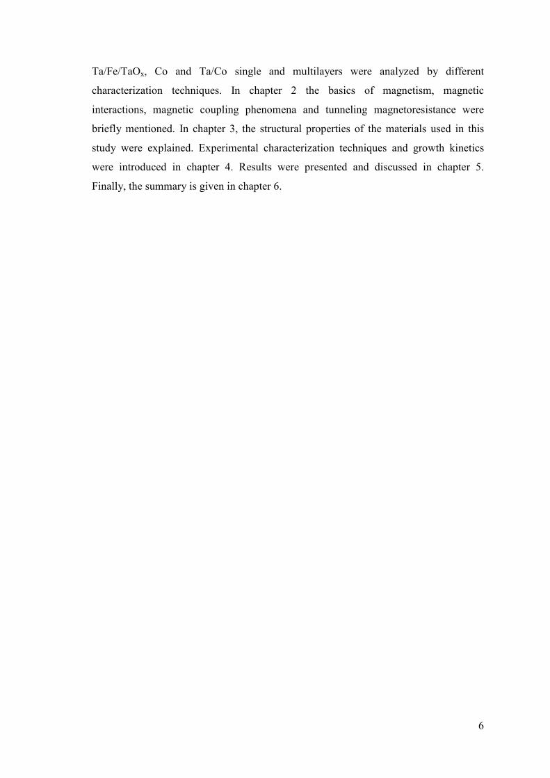
The surface morphology of Ta films on SiO2 substrate with various thicknesses
(6, 12, 18, 24 and 36 nm) was investigated. Figures 5.4 and Figure 5.5 shows the
surface morphology of 6 and 36 nm thick Ta films, respectively. The corresponding
roughnesses of Ta and Fe films with various thicknesses were shown in figure 5.6. is
seen that Ta film has quite smooth and uniform surface structure on SiO2 substrate. The
roughness is increasing at the beginning and then formation of continuous structure
results in a decrease in the roughness. Then, it increases again with increases thickness.
The maximum rms roughness was found to be ~2.36 Å for 36 nm thick Ta. These
results are desirable for obtaining smooth interfaces of MTJs.
30 40 50 60
0
500
1000
1500
2000
Inte
nsity
X= 6 nm .
X= 12 nm .
X= 18nm .
X= 24nm .
X= 36nm .
β−Τa (002 )
Fe (110 )
2222ΘΘΘΘ
43
Figure 5.4. AFM images of 6 nm thick Ta thin film. Rms roughness is 2.3 Å
Figure 5.5. AFM images of 36 nm thick Ta thin film. Rms roughness is 2.4 Å
44
10 20 30 40
0
2
4
6 Ta
Fe
Thickness (nm)
Ta rm
s roughness (A
0)
0
2
4
6
Fe rm
s ro
ughness (A
0)
Figure 5.6. Rms roughness of SiO2/Ta and SiO2/Fe single layers
5.2.2. SiO2/Fe and SiO2/Ta/Fe
Figures 5.7 and 5.8 show the surface topographic images of Fe films for 12 nm
and 72 nm thicknesses. For the 6 nm Fe film, the rms roughness was found to be 1,7 Å
and then it increases 4 Å for the 12 nm thick Fe film. Like the Ta film, rms roughness
decreases after the 12 nm thick Fe film and then it increases gradually. The reason for
this change can be related to the fact that increasing thickness until at a certain
thickness results in disappearing defects and inhomogenities (Entani, et al. 2005).
Furthermore, Fe film on SiO2 substrate starts to crystallize after the thickness of 12 nm.
Existing crystalline structure causes an increase in grain sizes and releasing the stress in
the film. Therefore, surface roughness reduces. Figure 5.6 also shows the rms roughness
of SiO2/Fe structures. The effect of Ta under layer on the surface roughness of Fe is
shown in figure 5.9. The rms roughness of 12 nm Fe film with 24 nm Ta under layer
was found to be 1.2 Å. Ta reduces the roughness of 12 nm Fe film from 4 Å to 1.2 Å.
This can be related to the increasing of structural properties of Fe film, resulting in an
increasing grain sizes.
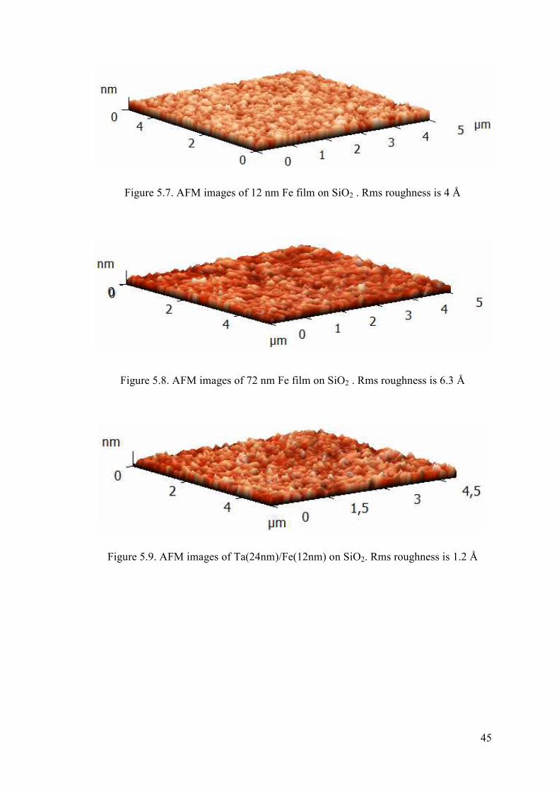
45
Figure 5.7. AFM images of 12 nm Fe film on SiO2 . Rms roughness is 4 Å
Figure 5.8. AFM images of 72 nm Fe film on SiO2 . Rms roughness is 6.3 Å
Figure 5.9. AFM images of Ta(24nm)/Fe(12nm) on SiO2. Rms roughness is 1.2 Å

46
5.3. Vibrating Sample Magnetometer
5.3.1. SiO2/Fe
Magnetic hysteresis loops of Fe layer with different thicknesses on SiO2
substrate are shown in the Figure 5.10. When the thickness of Fe film increases, the Hc
increases linearly. This result may be related to the increase of grain sizes with the
thickness of Fe layer as can seen from the XRD measurements. It is well known that if
the grain sizes increase, crystalline magnetic anisotropy increases within the each grain
and magnetization of each grain has a different orientation. In this case, magnetization
can not rotate at the same time causing an increase in the Hc for thicker films (Sharma,
et al. 2005).
The hysteresis loops are nearly square like shape and there is no magnetic
anisotropy indicating that magnetization reversal occurs via the domain walls motion
(Kumar and Gupta 2006, Swerts, et al. 2004). If coercivity is associated with domain
walls motion across the grain boundaries, than large grain sizes should results in low
Hc. However, we observed opposite results for Fe films. Large grains within the Fe
films are isolated and grain boundaries play a pinning effect on the domain wall
motions. They also cause the disappearance of the anisotropy.
For the 72 nm thick Fe, it is expected that surface roughness increases with
increasing thickness and pinning effects on the domain wall motion increases. In the
case of rough surface, magnetic poles are induced and in-plane demagnetizing field
occurs. This can cause a change in the thickness and sizes of domains. Step edges as a
result of rough surfaces also restrict the wall motion. In the magnetization reversal
process, external field not only overcomes the domain wall but also overcomes the
demagnetizing field. Therefore, domain wall pinning exists and Hc increases (Ng, et al.
2002).

47
Figure 5.10. The hysteresis loops of Fe thin film with different thicknesses on SiO2
5.3.2. SiO2/Ta/Fe
Figure 5.11. shows the effect of Ta buffer layer on the magnetic properties of Fe
film. It is seen that Ta buffer layer causes a significant increase, more than three times,
in Hc of 12 nm thick Fe film. When the crystallinities of the two layers are compared,
this significant increase can be attributed to the improvement of crystalline quality of
the Fe layer because of the Ta buffer layer. As it was discussed above, increasing of
crystalline quality results from the increasing grain sizes and large grains have large
magnetic anisotropy. In this case, each grain has an intrinsic magnetization which does
not interact with the other grains and magnetization reversal process occurs
independently, resulting in an increase in the Hc. Also the strain in the Fe film causes an
increase in the Hc.
-300 -200 -100 0 100 200 300
Norm
alized M
om
ent
Field (Oe)
Fe (72 nm)
Fe (36 nm)
Fe (24 nm)
Fe (12 nm)
Fe (6 nm)
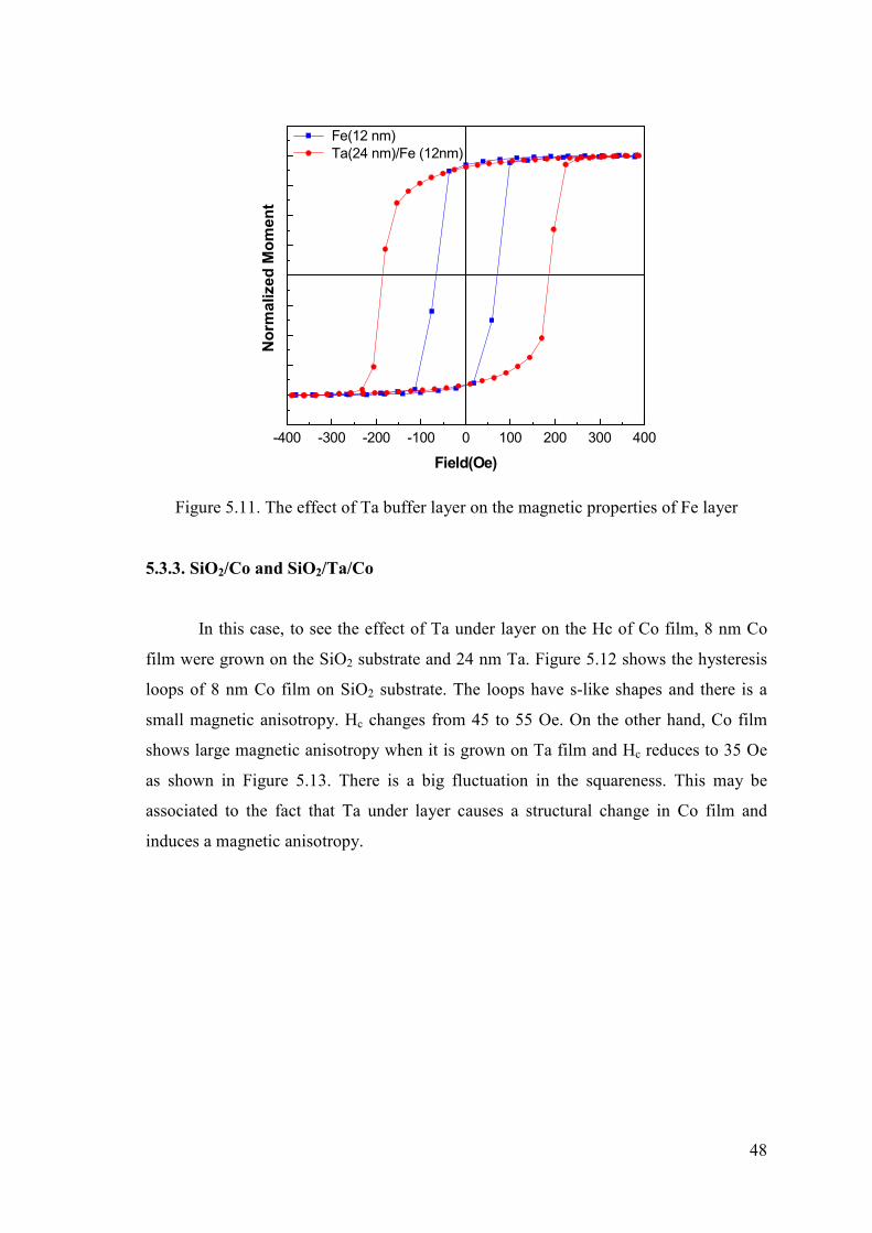
48
Figure 5.11. The effect of Ta buffer layer on the magnetic properties of Fe layer
5.3.3. SiO2/Co and SiO2/Ta/Co
In this case, to see the effect of Ta under layer on the Hc of Co film, 8 nm Co
film were grown on the SiO2 substrate and 24 nm Ta. Figure 5.12 shows the hysteresis
loops of 8 nm Co film on SiO2 substrate. The loops have s-like shapes and there is a
small magnetic anisotropy. Hc changes from 45 to 55 Oe. On the other hand, Co film
shows large magnetic anisotropy when it is grown on Ta film and Hc reduces to 35 Oe
as shown in Figure 5.13. There is a big fluctuation in the squareness. This may be
associated to the fact that Ta under layer causes a structural change in Co film and
induces a magnetic anisotropy.
-400 -300 -200 -100 0 100 200 300 400
Norm
alized M
om
ent
Field(Oe)
Fe(12 nm)
Ta(24 nm)/Fe (12nm)

49
-150 -100 -50 0 50 100 150
Norm
alized M
om
ent
Magnetic Field(Oe)
30
60
90
120
Figure 5.12. The angle dependent hysteresis curves of SiO2/Co(8nm)
-100 -75 -50 -25 0 25 50 75 100
Norm
alized M
om
ent
Magnetic Field (Oe)
0
30
45
60
90
Figure 5.13. The angle dependent hysteresis curves f SiO2/Ta(24nm)/Co(8nm)

50
5.3.4. SiO2/Ta/Fe, SiO2/Ta/Fe/Ta and SiO2/Ta/Fe/TaOx
After determination of the effect of Ta buffer layer, Ta and TaOx layers were
grown on the SiO2/Ta(24nm)/Fe(12nm) structure in order the observe the effect of TaOx
layers on the magnetic properties of the Fe film. Figure 5.14 shows the hysteresis loops
of Ta/Fe, Ta/Fe/Ta and Ta/Fe/TaOx. When a and b are compared in Figure 5.14, it is
seen that Ta capping layer causes an increase in the Hc of the Fe film from 185 to 218
Oe. The reason is that Ta capping layer prevents the oxidation of the Fe film. The low
Hc of the Ta/Fe film arises from the oxidation of the Fe film, resulting in decreasing the
crystallinity and grain size of Fe film. This situation is undesirable for MTJs because
formation of dead layer at the interfaces can effect the spin polarization of electrons.
The b and c compare the effect of Ta and TaOx top layers. The TaOx layer reduces the
Hc of Fe film from 218 to 165 Oe, when it is compared with the Ta capping layer. The
reduction of the Hc can be related to the oxidation effect as it is explained for the graph
a. However, the effect of sputtered TaOx is larger than normal oxidation.
Figure 5.14. The effect of Ta and TaOx capping layers on the Hc of Fe film
-300 -200 -100 0 100 200 300
c
Norm
alized M
om
ent
Field(Oe)
Ta/Fe/TaO
Ta/Fe/Ta
b
Ta/Fe
a

51
5.3.5. SiO2/Ta/Fe/TaOx
In the previous parts, we have investigated the effects of bottom and top layer
on the Hc and crystallinity of the Fe film. In this part, we determine the effect of
thickness of the bottom Ta buffer layer. We tried different Ta thickness with substrate
bias cleaning as a buffer layer. The Figure 5.15 shows the VSM results. The 6 nm Ta
layer causes the lowest Hc of the Fe film. However, there is a big jump in the Hc when
the thickness of the Ta layer is 12 nm. Then, increasing the Ta layer after that thickness
causes a linear decreasing in the Hc. There is no significant change between 24 nm and
36 nm. This can be explained by changes in the structure of Fe film. The 12 nm Ta film
creates the best crystalline Fe film with respect to the other. The structural properties of
the Fe film strongly affect the magnetic properties.
-400 -300 -200 -100 0 100 200 300 400
F i e l d ( O e )
36 nm
24 nm
18 nm
Norm
alized M
oment
12 nm
6 nm
Figure 5.15. Hysteresis loops of SiO2/Ta(d)/Fe(12nm)/TaOx(4nm) structure with
different Ta buffer layer thicknesses
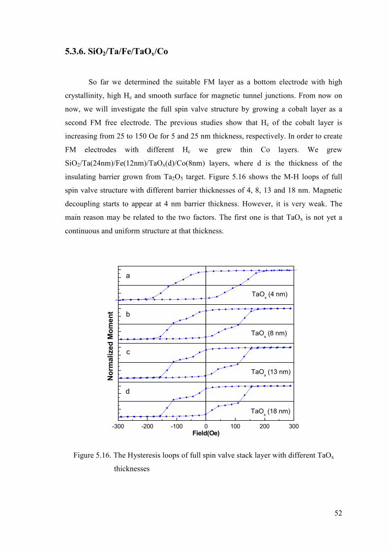
52
5.3.6. SiO2/Ta/Fe/TaOx/Co
So far we determined the suitable FM layer as a bottom electrode with high
crystallinity, high Hc and smooth surface for magnetic tunnel junctions. From now on
now, we will investigate the full spin valve structure by growing a cobalt layer as a
second FM free electrode. The previous studies show that Hc of the cobalt layer is
increasing from 25 to 150 Oe for 5 and 25 nm thickness, respectively. In order to create
FM electrodes with different Hc we grew thin Co layers. We grew
SiO2/Ta(24nm)/Fe(12nm)/TaOx(d)/Co(8nm) layers, where d is the thickness of the
insulating barrier grown from Ta2O5 target. Figure 5.16 shows the M-H loops of full
spin valve structure with different barrier thicknesses of 4, 8, 13 and 18 nm. Magnetic
decoupling starts to appear at 4 nm barrier thickness. However, it is very weak. The
main reason may be related to the two factors. The first one is that TaOx is not yet a
continuous and uniform structure at that thickness.
-300 -200 -100 0 100 200 300
Field(Oe)
TaOx (18 nm)
d
TaOx (13 nm)
c
Norm
alized M
om
ent
TaOx (8 nm)
b
a
TaOx (4 nm)
Figure 5.16. The Hysteresis loops of full spin valve stack layer with different TaOx
thicknesses
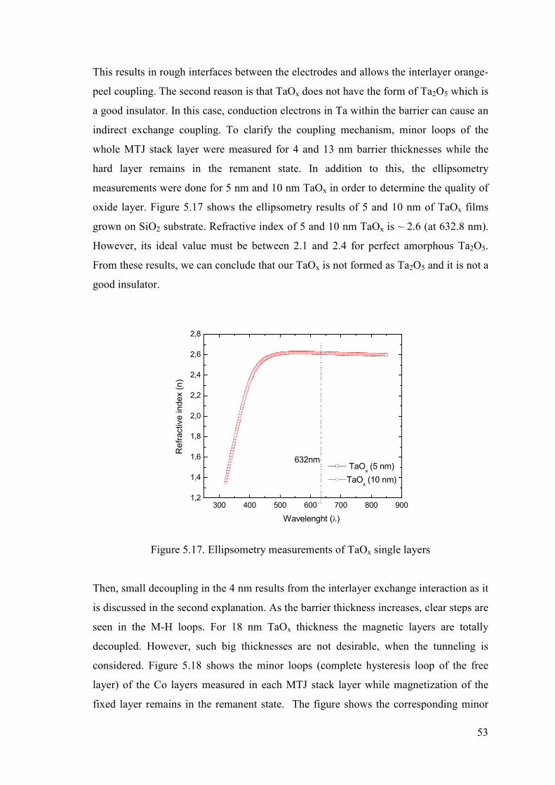
53
This results in rough interfaces between the electrodes and allows the interlayer orange-
peel coupling. The second reason is that TaOx does not have the form of Ta2O5 which is
a good insulator. In this case, conduction electrons in Ta within the barrier can cause an
indirect exchange coupling. To clarify the coupling mechanism, minor loops of the
whole MTJ stack layer were measured for 4 and 13 nm barrier thicknesses while the
hard layer remains in the remanent state. In addition to this, the ellipsometry
measurements were done for 5 nm and 10 nm TaOx in order to determine the quality of
oxide layer. Figure 5.17 shows the ellipsometry results of 5 and 10 nm of TaOx films
grown on SiO2 substrate. Refractive index of 5 and 10 nm TaOx is ~ 2.6 (at 632.8 nm).
However, its ideal value must be between 2.1 and 2.4 for perfect amorphous Ta2O5.
From these results, we can conclude that our TaOx is not formed as Ta2O5 and it is not a
good insulator.
300 400 500 600 700 800 9001,2
1,4
1,6
1,8
2,0
2,2
2,4
2,6
2,8
TaOx (5 nm)
TaOx (10 nm)
632nm
Refractive index (n)
Wavelenght (λ)
Figure 5.17. Ellipsometry measurements of TaOx single layers
Then, small decoupling in the 4 nm results from the interlayer exchange interaction as it
is discussed in the second explanation. As the barrier thickness increases, clear steps are
seen in the M-H loops. For 18 nm TaOx thickness the magnetic layers are totally
decoupled. However, such big thicknesses are not desirable, when the tunneling is
considered. Figure 5.18 shows the minor loops (complete hysteresis loop of the free
layer) of the Co layers measured in each MTJ stack layer while magnetization of the
fixed layer remains in the remanent state. The figure shows the corresponding minor
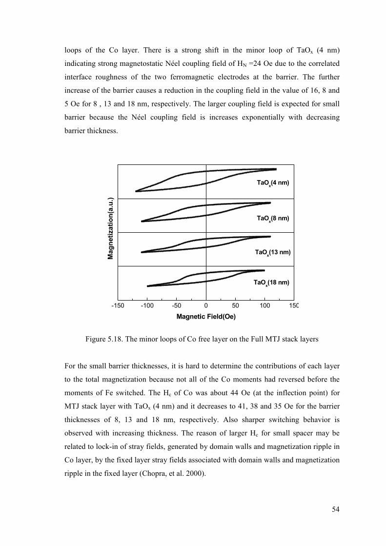
54
loops of the Co layer. There is a strong shift in the minor loop of TaOx (4 nm)
indicating strong magnetostatic Néel coupling field of HN =24 Oe due to the correlated
interface roughness of the two ferromagnetic electrodes at the barrier. The further
increase of the barrier causes a reduction in the coupling field in the value of 16, 8 and
5 Oe for 8 , 13 and 18 nm, respectively. The larger coupling field is expected for small
barrier because the Néel coupling field is increases exponentially with decreasing
barrier thickness.
-150 -100 -50 0 50 100 150
TaOx(18 nm)
Magnetization(a
.u.)
Magnetic Field(Oe)
TaOx(13 nm)
TaOx(8 nm)
TaOx(4 nm)
Figure 5.18. The minor loops of Co free layer on the Full MTJ stack layers
For the small barrier thicknesses, it is hard to determine the contributions of each layer
to the total magnetization because not all of the Co moments had reversed before the
moments of Fe switched. The Hc of Co was about 44 Oe (at the inflection point) for
MTJ stack layer with TaOx (4 nm) and it decreases to 41, 38 and 35 Oe for the barrier
thicknesses of 8, 13 and 18 nm, respectively. Also sharper switching behavior is
observed with increasing thickness. The reason of larger Hc for small spacer may be
related to lock-in of stray fields, generated by domain walls and magnetization ripple in
Co layer, by the fixed layer stray fields associated with domain walls and magnetization
ripple in the fixed layer (Chopra, et al. 2000).
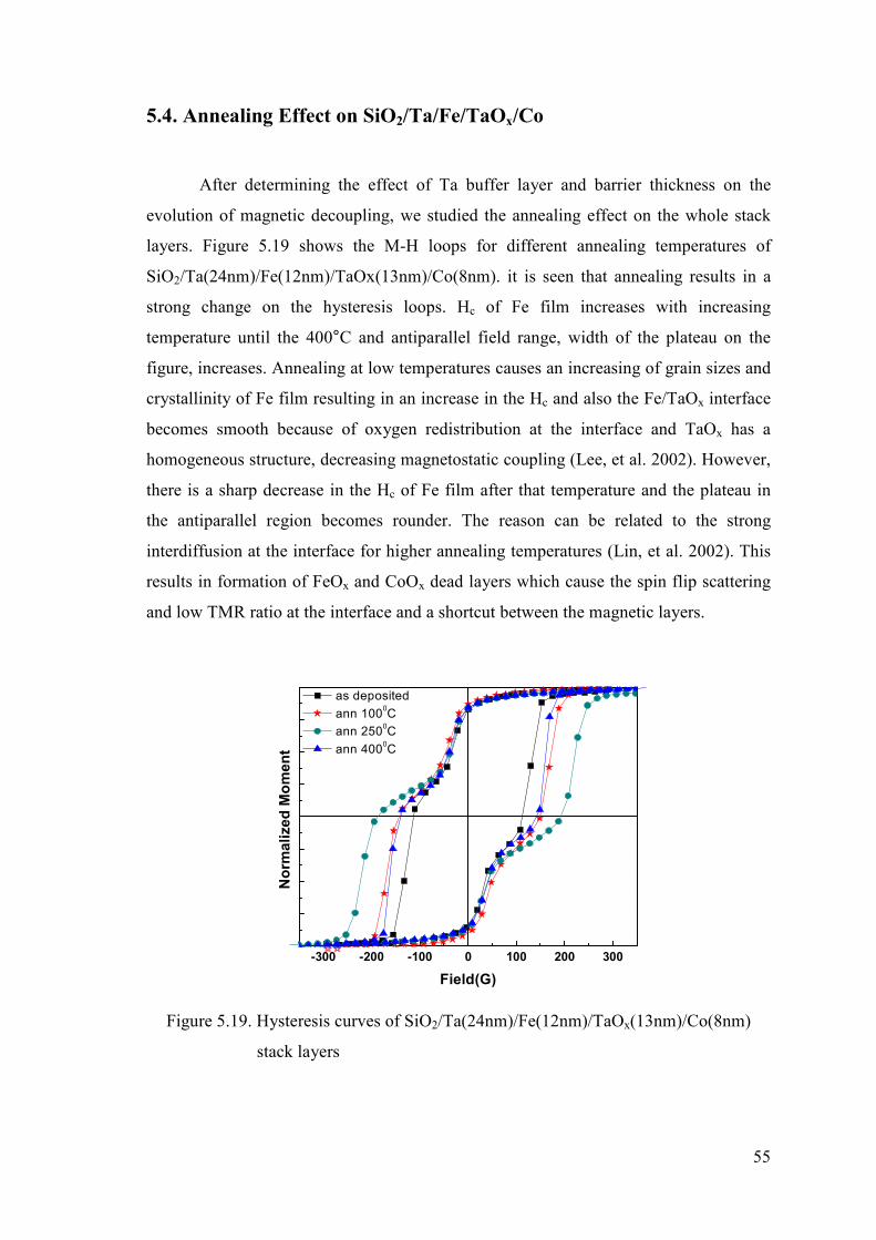
55
5.4. Annealing Effect on SiO2/Ta/Fe/TaOx/Co
After determining the effect of Ta buffer layer and barrier thickness on the
evolution of magnetic decoupling, we studied the annealing effect on the whole stack
layers. Figure 5.19 shows the M-H loops for different annealing temperatures of
SiO2/Ta(24nm)/Fe(12nm)/TaOx(13nm)/Co(8nm). it is seen that annealing results in a
strong change on the hysteresis loops. Hc of Fe film increases with increasing
temperature until the 400°C and antiparallel field range, width of the plateau on the
figure, increases. Annealing at low temperatures causes an increasing of grain sizes and
crystallinity of Fe film resulting in an increase in the Hc and also the Fe/TaOx interface
becomes smooth because of oxygen redistribution at the interface and TaOx has a
homogeneous structure, decreasing magnetostatic coupling (Lee, et al. 2002). However,
there is a sharp decrease in the Hc of Fe film after that temperature and the plateau in
the antiparallel region becomes rounder. The reason can be related to the strong
interdiffusion at the interface for higher annealing temperatures (Lin, et al. 2002). This
results in formation of FeOx and CoOx dead layers which cause the spin flip scattering
and low TMR ratio at the interface and a shortcut between the magnetic layers.
-300 -200 -100 0 100 200 300
Norm
alized M
om
ent
Field(G)
as deposited
ann 1000C
ann 2500C
ann 4000C
Figure 5.19. Hysteresis curves of SiO2/Ta(24nm)/Fe(12nm)/TaOx(13nm)/Co(8nm)
stack layers
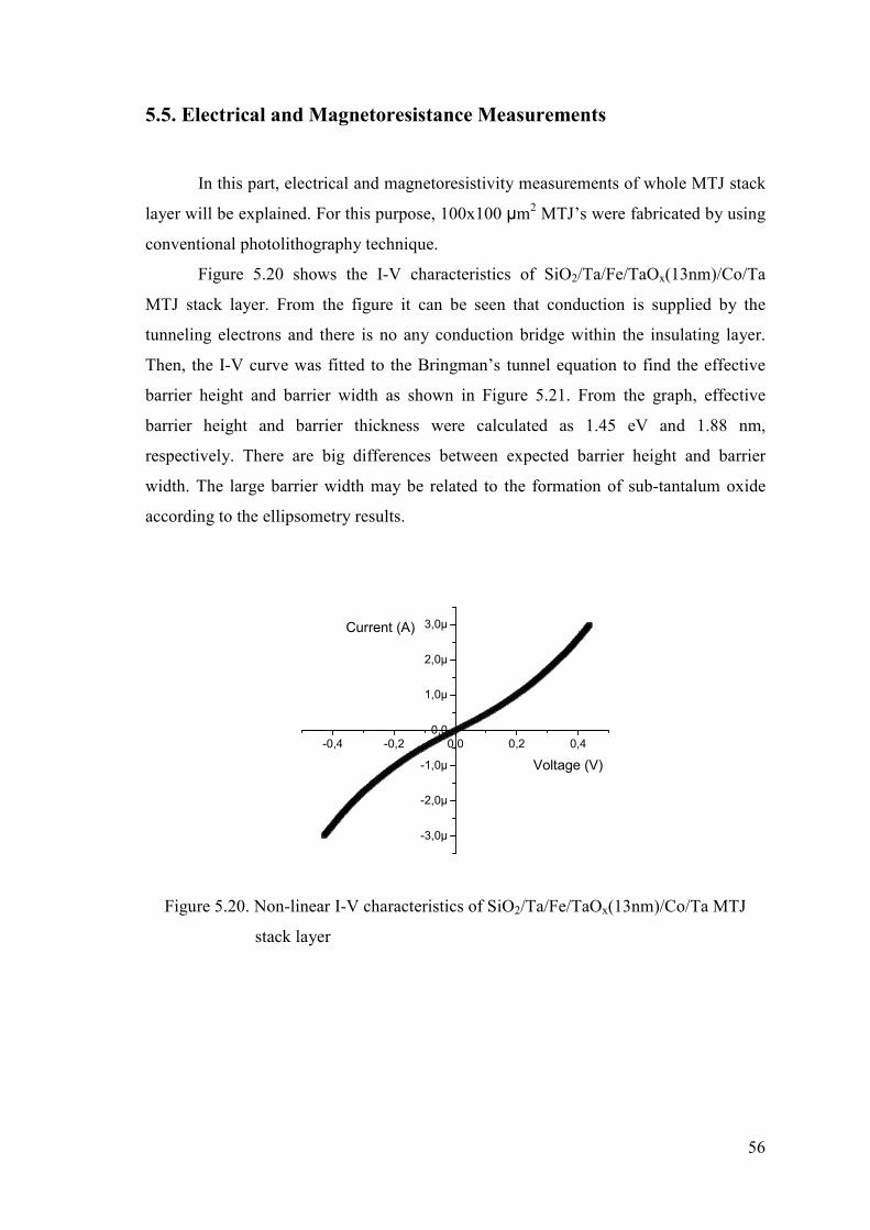
56
-0,4 -0,2 0,0 0,2 0,4
-3,0µ
-2,0µ
-1,0µ
0,0
1,0µ
2,0µ
3,0µCurrent (A)
Voltage (V)
5.5. Electrical and Magnetoresistance Measurements
In this part, electrical and magnetoresistivity measurements of whole MTJ stack
layer will be explained. For this purpose, 100x100 µm2 MTJ’s were fabricated by using
conventional photolithography technique.
Figure 5.20 shows the I-V characteristics of SiO2/Ta/Fe/TaOx(13nm)/Co/Ta
MTJ stack layer. From the figure it can be seen that conduction is supplied by the
tunneling electrons and there is no any conduction bridge within the insulating layer.
Then, the I-V curve was fitted to the Bringman’s tunnel equation to find the effective
barrier height and barrier width as shown in Figure 5.21. From the graph, effective
barrier height and barrier thickness were calculated as 1.45 eV and 1.88 nm,
respectively. There are big differences between expected barrier height and barrier
width. The large barrier width may be related to the formation of sub-tantalum oxide
according to the ellipsometry results.
Figure 5.20. Non-linear I-V characteristics of SiO2/Ta/Fe/TaOx(13nm)/Co/Ta MTJ
stack layer
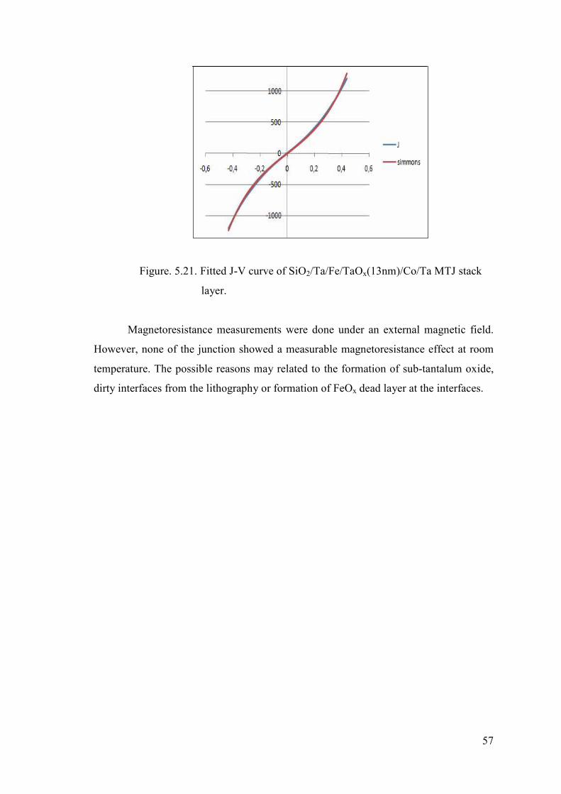
57
Figure. 5.21. Fitted J-V curve of SiO2/Ta/Fe/TaOx(13nm)/Co/Ta MTJ stack
layer.
Magnetoresistance measurements were done under an external magnetic field.
However, none of the junction showed a measurable magnetoresistance effect at room
temperature. The possible reasons may related to the formation of sub-tantalum oxide,
dirty interfaces from the lithography or formation of FeOx dead layer at the interfaces.
58
CHAPTER 6
CONCLUSIONS
In this study, structural and magnetic properties of SiO2/Ta/Fe/TaOx/Co
multilayer were studied. To build up a good magnetic multilayer, Fe, Co, Ta/Fe, Ta/Co,
Ta/Fe/TaOx single and multilayers were investigated by AFM, XRD, VSM and
ellipsometry characterization techniques. Then electrical and magnetoresistance
measurements were done by conventional four point probe technique.
XRD results showed that Fe film starts to gain crystalline order at 12 nm
thickness on SiO2 substrate and its crystallinity increases with increasing thickness.
Using 24 nm Ta buffer layer causes large increase in the crystallinity of Fe peak. The
crystallinity of the Ta under layer also affects the structural and magnetic properties of
Fe film.
AFM results showed that Fe films have very smooth surfaces and their rms
roughness change from 1.7 Å to 6.3 Å for the thicknesses between 6 nm and 72 nm. For
small thicknesses roughness first increases up to 4 Å and then decreases with increasing
thickness. This shows the formation of uniform film and transition from amorphous
phase to crystalline structure. For larger thicknesses, rms value increases with
increasing thickness. The same situation was seen in the Ta buffer layer.
VSM measurements showed that magnetic properties of magnetic films were
strongly affected by structural properties of the films. Hc of Fe film increased with
increasing thickness. When it was compared with the XRD data, it was seen that Hc of
Fe film strongly depended on the crystalline structure. Furthermore, the films did not
show any magnetic anisotropy. This shows that the magnetization reversal is dominated
by domain walls motion. Formation of crystalline structure caused domain wall pinning
centers at the grain boundaries. This caused the disappearance of the anisotropy within
the films. Moreover, magnetic properties of films also were strongly affected by
crystalline structure of under layer.
To see the oxygen effect on the Hc of Fe film, TaOx and Ta capping layers were
grown on Fe films and they were compared with the as-deposited Fe film (oxidized
with air). The results indicated that the Hc of Fe film was smallest one with TaOx

59
capping layer film while the Ta capping layer made the highest Hc of Fe. It was
concluded that there was oxygen diffusion into the Fe layer resulting in reduction of
crystallinity. When the coercivities of as deposited and TaOx capping Fe films
compared, we saw that the effect of oxygen diffusion was higher in the case of
Fe/TaOx.
Co minor loops showed that there is strong magnetostatic coupling between FM
layers. The strength of coupling is large for thin TaOx barrier and it is small for thicker
TaOx. The reason can be related to the formation of non-uniform and sub tantalum-
oxide instead of Ta2O5 as well as large Neel orange peel coupling.
Annealing of the MTJ structure improves the magnetic decoupling and Hc of
Fe. However, when the temperature reached to the 400°C, there was a strong reduction
in both Hc of Fe and decoupling mechanism. The reason was associated with the
increasing annealing temperature increases the crystalline quality of Fe up to the 250 °C
and increases the Hc of Fe. Also annealing causes the formation of smooth interface,
resulting in a decrease of the orange-peel coupling. In contrast, higher annealing
temperatures cause the oxygen diffusion between Fe and TaOx interfaces. Therefore,
FeOx dead layer may exist at the interface, which causes the reduction in Hc of Fe.
Finally, 100x100 µm2 MTJs were fabricated by conventional photolithography
technique. Then, electrical measurements showed non-linear I-V characteristics and
effective barrier height and barrier width were found 1.45 eV and 1.88 nm, respectively.
Magnetoresistance measurements were done under an external magnetic field.
However, none of the junctions showed a measurable magnetoresistance effect at room
temperature.
60
REFERENCES
Baibich, M.N., J.M. Broto, A. Fert, Van Dau F. Nyugen, F. Petroff, P. Eitenne, G.
Creuzet, A. Friederich, and J. Chazelas. 1988. Giant magnetoresistance of (001)Fe/(001)Cr magnetic superlattices. Physical Review Letters 61 (21):2472
Binash, G., P. Grünberg, F. Saurenbach and W. Zinn. 1989. Enhanced Magnetoresistance in layered magnetic structures with antiferromagnetic interlayer exchange. Physical Review B 39 (7):4828-4830.
Bowen, M., M. Bibes, A. Barthélémy, J.P. Contour, A. Anane, Y. Lemaitre and A. Fert. 2003. Nearly total spin polarization in La2/3Sr1/3MnO3 from tunneling experiments. Applied Physics Letters 82:233-235.
Bowen, M., V. Cros, F. Petroff, A. Fert, C. M. Boubeta, J.L. Costa-Krämer, J.M. Anguita, A. Cebollada, F. Briones, J.M. de Terasa, L. Morellón, M.R. Ibarra, F. Güell, F. Peiró and A. Cornet. 2001. Large magnetoresistance in Fe/MgO/FeCo(001) epitaxial tunnel junctions on GaAs(001). Applied Physics
Letters 79:1655-1657.
Brinkman, W.F., R.C. Dyness, and J.M. Rowell. 1970. Tunneling conductance of asymmetrical barriers. Journel of Applied Physics 45:1915-1921.
Cullity, B.D. and S.R. Stock, 2001. Elements of x-ray diffraction. New Jersey: Prentice Hall.
Djayaprawira, D.D., K. Tsunekawa, M. Nagai, H. Maehara, S. Yamagata, N. Watanabe, S. Yuasa, Y. Suzuki and K. Ando. 2005. 230% room-temperature magnetoresistance in CoFeB/MgO/CoFeB magnetic tunnel junctions. Applied
Physics Letters 86:92502
Entani, S., M. Kiguchi, S. Ikeda and K. Saiki. 2005. Magnetic properties of ultrathin
cobalt films on SiO2 substrates. Thin Solid films 493:221-225.
Han, X. F., M. Oogane, H. Kubota, Y. Ando and T. Miyazaki. 2000. Fabrication of high-magnetoresistance tunnel junctions using Co75Fe25 ferromagnetic electrodes. Applied Physics Letters 77:283–285.
61
Hardley, M. J., R. Atkinson and R. J. Pollard. 2002. Magnetic properties of Co films deposited onto obliquely sputtered Ta underlayer. Journal of Magnetism and
Magnetic Materials 246:347-350.
Hehn, M., O. Lenoble, D. Lacour and A. Schuhl. 2000. Magnetic anisotropy and domain duplication in transport properties of tunnel junctions. Physical Review B 62(17):11344-11346.
Hook, J. R. and Hall, H. E. 1995. Solid State Physics. Chicester: John Wiley & Sons.
Jiang, A., T.A. Tyson, L. Axe, L. Gladczuk, M. Sosnowski, P. Cote. 2005. The structure and stability of β-Ta thin films. Thin Solid Film 479:166-173.
Jullière, M. 1975. Tunneling between ferromagnetic films. Physics Letters 54A(3): 225-226.
Kumar, G. 2004. Structural and magnetic characterization of Nd-based Nd-Fe and Nd-Fe-Co-Al metastable alloys. Technical University Dresden Thesis of Ph.D
Kumar, D., and A. Gupta. 2007. Evolution of structural and magnetic properties of sputtered nanocrystalline Co thin films with thermal annealing. Journal of
Magnetism and Magnetic Materials 308:318-324.
Lee, K. I., J. H. Lee, W.Y. Lee, K.W. Rhie, J. G. Ha, C.S. Kim and Shin K. H. 2002. Enhanced tunneling magneroresistance and thermal stability of magnetic tunnel junction by rapid anneal. Journal of Magnetism and Magnetic Materials 239:120-122.
Lee, Y. M., J. Hayakawa, S. Ikeda, F. Matsukura, H. Ohno. 2007. Effect of electrode composition on the tunnel magnetoresistance of pseudo-spin-valve magnetic tunnel junction with a MgO tunnel barrier. Applied Physics Letters 90(212507):1-3.
Lin, M.T., C.H. Ho, Y.D. Yao, R.T. Huang, C.C. Liao, F.R. Chen and J.J. Kai. 2002. Interface characterization and thermal stability of Co/Al-O/CoFe spin-dependent tunnel junctions. Journal of Applied Physics 91(10):7475-7477.
Liu, L., H. Gong, Y. Wang, J. Wang, A.T.S. Wee and R. Liu. 2001. Annealing effects of Tantalum thin films sputtered on [001] Silicon substrate. Materials Science
Engineering C (16):85-89.

62
Magnusson, J., E. Papadopoulou, P. Svedlindh and P. Nordblad. 1997. AC susceptibility of a paramagnetic Meissner effect sample. Physica C 297:317-325.
Meiklejohn, W. P. and C. P. Bean. 1957. New magnetic anisotropy. Physical Review B 105:904.
Miyazaki, T. and N. Tezuka. 1995. Giant magnetic tunneling effect in Fe/Al2O3/Fe Junction. Journal of Magnetism and Magnetic Materials 139(3):231.
Moodera, J.S., L.R. Kinder, T.M. Wong and R. Meservey. 1995. Large magnetoresistance at room temprature in ferromagnetic thin film tunnel junctions. Physical review letters 74(16):3273-3276.
Mott, N.F. 1936. The electrical conductivity of transition metals. Proc. Roy. Soc.
London A 153:699.
Ng, V., J.F. Hu, A.O. Adeyeye, J.P. Wang and T.C. Chong. 2002. Radio frequency substrate bias effect on properties of Co thin film and multileyer structures. Journal of Magnetism and Magnetic Materials 247:339-344.
Park, M.H., Y.K. Honk, S.H. Gee, M.L. Mottern and T.W. Jang. 2002. Difference in coercivity between Co/Fe and Fe/Co bilayers. Journal of Applied Physics 91(10):7218-7220.
Parkin, S.S., C. Kaiser, A. Panchula, P.M. Rice, B. Hughes, M. Samant and S.H. Yang. 2004. Giant tunnelling magnetoresistance at room temperature with MgO (100) tunnel barriers. Nature Materials 3:862-867
Rottländer, P., M. Hehn, O. Lenoble and A. Schuhl. 2001. Tantalum oxide as an alternative low height tunnel barrier. Applied Physics Letter 78 (21): 3274-3276.
Schuhl, A. and Lacour, D. 2005. Spin dependent transport: GMR & TMR. Comptes
Rendus Physique. Vol. 6, pp. 945-955.
Sharma, A., R. Brajpuriya, S. Tripathi and S.M. Chaudhari. 2005. Study of annealed Co thin films deposited by ion beam sputtering. Journal of Vacuum Science
Technology A 24 (1):74-77.

63
Sharma, P. and A. Gupta. 2005. Effect of preparation condition on the soft magnetic properties of FeCuNbSiB thin film. Journal of Magnetism and Magnetic
Materials 288:347-353.
Simmons, J.G. 1963. Generelized formula for the electric tunnel effect between similar electrodes seperated by a thin insulating film. Journal of Applied Physics 34(6):1793.
Sousa, R.C., J.J. Sun, V. Soares, P.P. Freitas, A. Kling, M.F. da Silva and J.C. Soares. 1998. Applied Physics Letter 73 (1998):3288.
Sun, J.J., V. Soares, P.P. Freitas, A. Kling, M.F. da Silva and J.C. Soares. 1998. Large
tunneling magnetoresistance enhancement by thermal anneal. Applied Physics
Letters 73:3288-3290.
Swerts, J., S. Vandelande, K. Temst and C.V. Haesendonck. 2004. Surface roughness effects on the magnetization reversal of polycrstalline Fe/Ag thin films. Solid
Stade Communications 131:359-363.
Thomson, W. 1856. On the electro-dynamic qualities of metals: Effects of magnetization on the electric conductivity of Nickel and of Iron. The Royal
Society of London 8:546-550.
Wang, D., C. Nordman, J.M. Daughton, Z. Qian and J. Fink. 2004. 70% TMR at room temperature for SDT sandwich junctions with CoFeB as free and reference layers. IEEE Transaction on Magnetics 40:2269-2271.
Wang, D., J.M. Daughton, D. Reed, W.D. Wang and J.Q. Wang. 2000. Magnetostatic coupling in spin dependent tunnel junctions. IEEE Transactions on Magnetics. 36(5):2802-2805
Yuasa, S., T. Nagahama, A. Fukushima, Y. Susuki and K. Ando. 2004. Giant room-temperature magnetoresistance in single-crystal Fe/MgO/Fe magnetic tunnel junctions. Nature Materials 3:868-871.


