The Future of Electrical I/O for Microprocessors › r5 › denver › sscs › Presentations ›...
51
1 The Future of Electrical I/O for Microprocessors Frank O’Mahony [email protected] Intel Labs, Hillsboro, OR USA
Transcript of The Future of Electrical I/O for Microprocessors › r5 › denver › sscs › Presentations ›...

1
The Future of Electrical I/O for
Microprocessors
Frank O’Mahony
Intel Labs, Hillsboro, OR USA
2
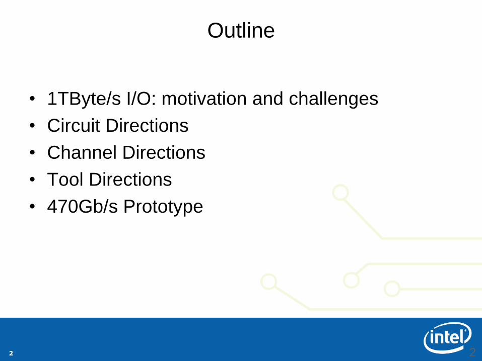
Outline
• 1TByte/s I/O: motivation and challenges
• Circuit Directions
• Channel Directions
• Tool Directions
• 470Gb/s Prototype
2

3
Microprocessor Bandwidth Needs
• As CPU core count increases, I/O bandwidth (BW) requirements will increase for all segments
• Current system bandwidth requirements (Y2010)– Client BW = ~50GB/s
– Server BW = ~100GB/s
– High-end Server BW = ~200GB/s
Server
Example
High-End
Server Example

4
Microprocessor Bandwidth Trends
Bandwidth Drivers:
CPUMemory
CPUCPU
CPUPeripheral
CPUI/O bridge0.1
1
10
100
1000
Bandw
idth
(G
B/s
)
2000 2005 2010 2015
2X/2yrs.
3X/2yrs.
4
High-end microprocessors are expected to
need ~1TB/s during coming decade

5
Microprocessor I/O Power
• Current system I/O power efficiency is 20-40pJ/bit
• If I/O power efficiency doesn’t improve during the next decade, then:
1TB/s x 20pJ/bit = 160W
System BW I/O Pwr. Eff. I/O Pwr
Client ~50GB/s 20pJ/bit 8W
Server ~100GB/s 20pJ/bit 16W
High-End Server
~200GB/s 20pJ/bit 32W

6
I/O Energy Efficiency Trends
1
10
100
Energy Eff.
(pJ/bit)
2002 2004 2006 2008
-20%/year
Issue: ~20% per year power reduction while bandwidth
increasing 40-70% per year
Year
2010
Ref: R. Palmer,
ISSCC ‘07

7
Energy Efficiency and Channel Loss Tradeoff
• Power efficiency is strongly correlated to channel loss
• Simply scaling per-pin BW will not meet power budget
• Low power interfaces should be “wider” not faster
Based on transceivers
reported 2006-2009 in
65-130nm CMOS
10
100
Energy Eff.
(pJ/bit)
0 10 20 30 401
Channel Loss @ Symbol rate (dB)
7

8
Channel/Interconnect Density
• Conventional package/socket density does not
scale with process
• “Width” of interfaces is limited by routing
congestion
C4 pitch << Pkg. pin pitch
Flip-chip Package
µP
Circuit
area
C4 bump
area
Time
Density

9
Problem Statement Summary
• Bandwidth needs are quickly approaching 1TB/s
• Energy efficiency is not scaling as aggressively
as bandwidth
• The channel limits our ability to increase per-pin
data rate and/or increase the width of an
interface

10
How Will Electrical I/O scale to 1TB/s?
1. Co-design the interconnects and I/O circuitry to
meet bandwidth, scalability and power
efficiency demands
2. Scale the channel by transitioning to new
channel configurations and materials
3. Use accurate, statistical link design tools to
identify balanced architectures.

11
Outline
• 1TByte/s I/O: motivation and challenges
• Circuit Directions
• Channel Directions
• Tool Directions
• 470Gb/s Prototype
11
12
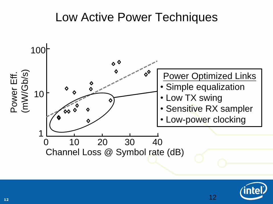
Low Active Power Techniques
12
10
100
0 10 20 30 401
Channel Loss @ Symbol rate (dB)
Pow
er
Eff.
(mW
/Gb
/s)
Power Optimized Links
• Simple equalization
• Low TX swing
• Sensitive RX sampler
• Low-power clocking

13
Minimize analog circuit complexity
RX
L
RTERM
CPAD
Ref: G. Balamurugan, JSSC 4/08
Lowest power links find ways to simplify equalization and
clocking circuitry to reduce power
Equalization examples:
Constrain equalization range by known channel characteristics
Continuous-time linear Rx equalizer
13

14
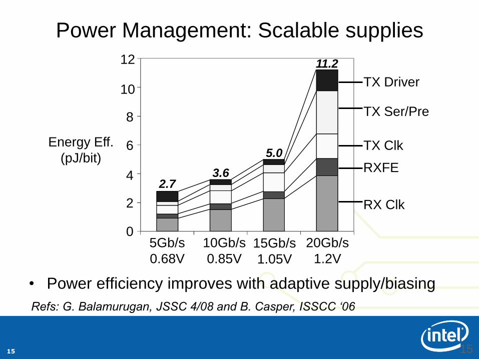
Power Management: Scalable supplies
• Adapt supply to frequency, process, temperature (f,P,T)
– Digital: Power VSUPPLY2∙f
– Analog: Power VSUPPLY∙Ibias
• Removes excess circuit BW and headroom
VR
VSUPPLY
TX
RX
VREG(f,P,T)
+
-
VREG(f,P,T)
CREG
VREF
VSUPPLY
Regulated supply ring VCO Data link with adaptive supply
14
15
Power Management: Scalable supplies
• Power efficiency improves with adaptive supply/biasing
2.73.6
5.0
11.2
5Gb/s
0.68V
10Gb/s
0.85V
15Gb/s
1.05V
20Gb/s
1.2V
Energy Eff.
(pJ/bit)
0
2
4
6
8
10
12
TX Driver
TX Ser/Pre
TX Clk
RXFE
RX Clk
Refs: G. Balamurugan, JSSC 4/08 and B. Casper, ISSCC ‘06
15

16
Aggressive Power Management
• Don’t spend power doing nothing!
• Rapidly adapt to bandwidth demand
– Requires fast, granular bandwidth adaptation
1.0
0.8
0.6
0.4
0.2
0.0
Normalized
Bandwidth
Demand
Time

17
Aggressive Power Management
1.0
0.8
0.6
0.4
0.2
0.0
Normalized
Bandwidth
Demand
Time
Conventional (fixed Bandwidth)
Wasted
Energy
• Don’t spend power doing nothing!
• Rapidly adapt to bandwidth demand
– Requires fast, granular bandwidth adaptation

18
Energy
Savings
Aggressive Power Management
1.0
0.8
0.6
0.4
0.2
0.0
Normalized
Bandwidth
Demand
Time
Conventional (fixed Bandwidth)
Adaptive
Bandwidth
• Don’t spend power doing nothing!
• Rapidly adapt to bandwidth demand
– Requires fast, granular bandwidth adaptation

19
Device Variation in Scaled CMOS
• Device manufacturing
tolerances are improving
• …but area scaling still
causes higher variation
• Fundamental power/area to
variation tradeoff is not
acceptable
Ref: K. Kuhn, IEDM 2007
LeffWeff
c
2
1σV 2
T
19
Need circuit architectures
that fundamentally change
this tradeoff.

20
Mitigating Device Variation
+-Voffset
Circuit derivatives (gm, ro)
are not calibrated by offset
calibration PSRR is not
calibrated
20
• Calibration greatly improves the
power/variation tradeoff
– Receiver offset calibration
– Duty cycle correction
– Adaptive equalizers
– Clock recovery (or deskew)
• Simple calibration doesn’t
alleviate all variation issues (e.g.
PSRR)

21
Mitigating Device Variation• Calibration greatly improves the
power/variation tradeoff
– Receiver offset calibration
– Duty cycle correction
– Adaptive equalizers
– Clock recovery (or deskew)
• Simple calibration doesn’t
alleviate all variation issues (e.g.
PSRR)
• Possible solutions:
– “Dynamic” calibration (e.g. auto-zero)
– Redundancy/reconfigurability
– Better “correct by design” circuits
ΦN
Φ1
selΦ
DSM
ΦOUT
Ref:
P. Hanumolu,
JSSC 2/08.
Coarse
Phase
gen.Φ LPF
DN
L (
ps)
INL (
ps)
21

22
Outline
• 1TByte/s I/O: motivation and challenges
• Circuit Directions
• Channel Directions
• Tool Directions
• 470Gb/s Prototype
22
23
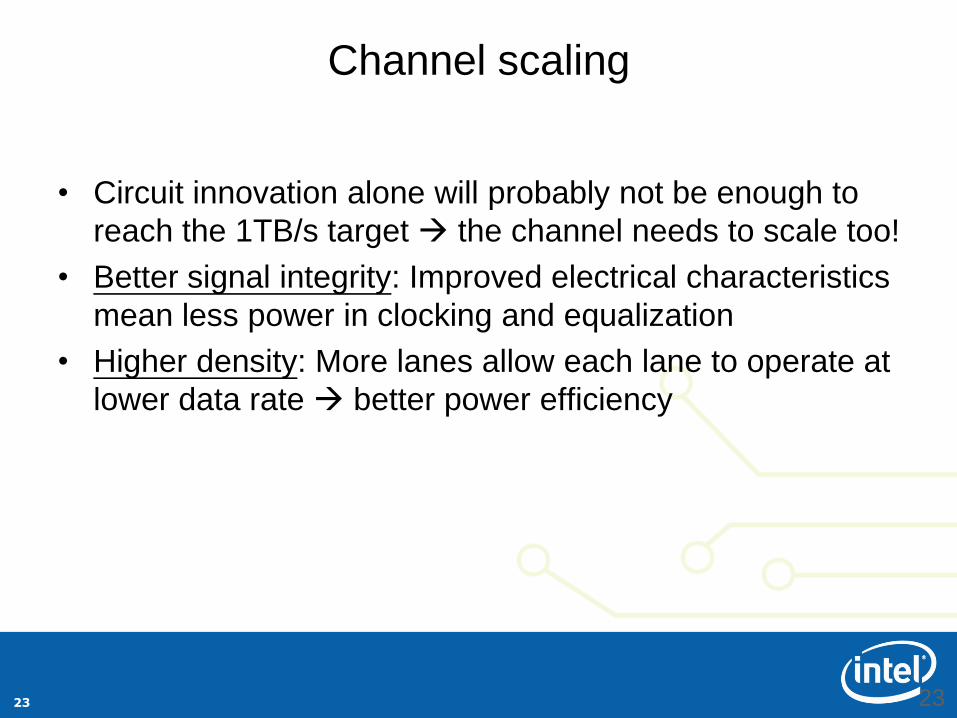
Channel scaling
• Circuit innovation alone will probably not be enough to
reach the 1TB/s target the channel needs to scale too!
• Better signal integrity: Improved electrical characteristics
mean less power in clocking and equalization
• Higher density: More lanes allow each lane to operate at
lower data rate better power efficiency
23

24
Channel vs. Equalization tradeoffs:
Backplane example
-80dB
-60dB
-40dB
0dB
0GHz 5GHz 15GHz
-20dB
10GHz
5mm Stubbed-via BP
Drilled-via BP
Ref: B. Casper, CICC ‘07.
24
|S21|
25
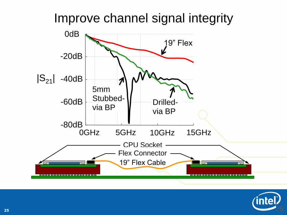
Improve channel signal integrity
19” Flex
-80dB
-60dB
-40dB
0dB
0GHz 5GHz 15GHz
-20dB
10GHz
5mm Stubbed-via BP
Drilled-via BP
19” Flex Cable
CPU SocketFlex Connector
25
|S21|

26
High density channels
10
1000
Ap
pro
x.
Co
nta
ct/
Ro
utin
g
Pitch
(µ
m)
100
1
Contact pitch
Routing pitch
26

27
High density channels
10
1000
Ap
pro
x.
Co
nta
ct/
Ro
utin
g
Pitch
(µ
m)
100
1
Contact pitch
Routing pitch
27

28
High density channels
10
1000
Ap
pro
x.
Co
nta
ct/
Ro
utin
g
Pitch
(µ
m)
100
1
Contact pitch
Routing pitch
28

29
High density channels
10
1000
Ap
pro
x.
Co
nta
ct/
Ro
utin
g
Pitch
(µ
m)
100
1
Contact pitch
Routing pitch
29

30
High density channels
10
1000
Ap
pro
x.
Co
nta
ct/
Ro
utin
g
Pitch
(µ
m)
100
1
Contact pitch
Routing pitch
30
31
Outline
• 1TByte/s I/O: motivation and challenges
• Circuit Directions
• Channel Directions
• Tool Directions
• 470Gb/s Prototype
31

32
What is the “Right” Link Architecture?
• Designers need the ability to quickly and
accurately compare architecture options
32
TX RX
Clock Jitter?
Signal Swing?
Equalization?
ISI? Xtalk?
Modulation (PAM)?
Data Rate?
Interface width?
Clock Jitter?
Sensitivity?
Equalization?

33
Empirical Approach
33
Simulate system with random data
This doesn’t provide adequate accuracy
(BER<10-12)
34
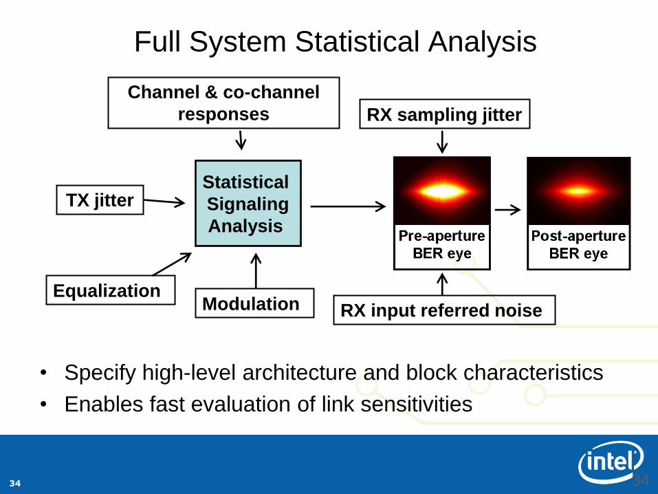
Full System Statistical Analysis
• Specify high-level architecture and block characteristics
• Enables fast evaluation of link sensitivities
Statistical
Signaling
Analysis
TX jitter
Channel & co-channel
responses
EqualizationModulation RX input referred noise
RX sampling jitter
34

35
Maximum Data Rate Comparison:
Backplane vs. Flex
TX FIR taps
DFE taps
1 2 3 4 5 6 4
128
4
1
4
2
4
8
4
16
4
32
4
64
4
4
30Gb/s
15Gb/s
45Gb/s
FlexM
ax. D
ata
Ra
te (
BE
R=
10
-12)
Drilled-via BP
Stubbed-via BP
35
• Statistical system analysis provides designers with real
performance tradeoffs and “brick walls”

36
Maximum Data Rate Comparison:
Backplane vs. Flex
• Statistical system analysis provides designers with real
performance tradeoffs and “brick walls”
TX FIR taps
DFE taps
1 2 3 4 5 6 4
128
4
1
4
2
4
8
4
16
4
32
4
64
4
4
30Gb/s
15Gb/s
45Gb/s
FlexM
ax. D
ata
Ra
te (
BE
R=
10
-12)
Drilled-via BP
Stubbed-via BP
36

37
Outline
• 1TByte/s I/O: motivation and challenges
• Circuit Directions
• Channel Directions
• Tool Directions
• 470Gb/s Prototype
37
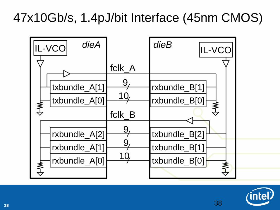
38
txbundle_A[1] rxbundle_B[1]
rxbundle_B[0]txbundle_A[0]
IL-VCOIL-VCO
rxbundle_A[1] txbundle_B[1]
txbundle_B[0]rxbundle_A[0]
rxbundle_A[2] txbundle_B[2]
dieA dieB
fclk_A
9
10
9
9
10
fclk_B
47x10Gb/s, 1.4pJ/bit Interface (45nm CMOS)
38

39
Bundled Architecture
Deskew
Deskew
Deskew
Deskew
Deskew
clk
RX sampler
RX sampler
RX sampler
RX sampler
RX sampler
data
Conventional:
Independent clocking

40
Bundled Architecture
• Clocking innovation Bundle clocking
Deskew
Deskew
Deskew
Deskew
Deskew
clk clk
Bundle
Deskew
RX sampler
RX sampler
RX sampler
RX sampler
RX sampler
data
Conventional:
Independent clocking

41
Bundled Architecture
• Clocking innovation Bundle clocking
Deskew
Deskew
Deskew
Deskew
Deskew
clk clk
RX sampler
RX sampler
RX sampler
RX sampler
RX sampler
RX sampler
RX sampler
RX sampler
RX sampler
RX sampler
data data
Bundled clocking reduces I/O power
Conventional:
Independent clocking
Optimized:
Bundle clocking
Bundle
Deskew
42
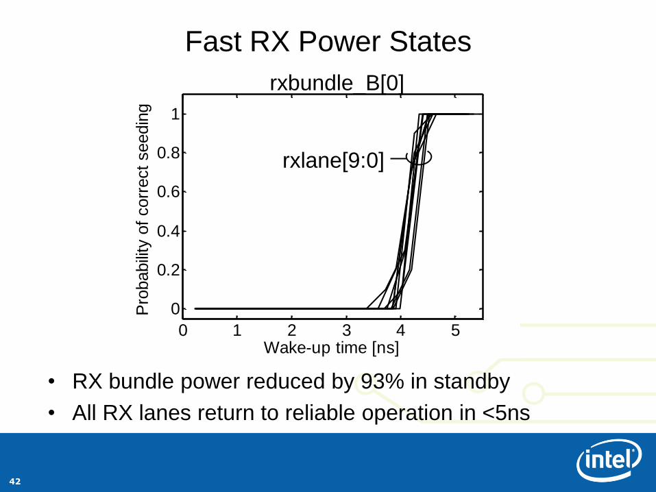
Fast RX Power States
• RX bundle power reduced by 93% in standby
• All RX lanes return to reliable operation in <5ns
0 1 2 3 4 5
0
0.2
0.4
0.6
0.8
1
Wake-up time [ns]
Pro
babili
ty o
f corr
ect
seedin
g
1rxbundle_B[0]
rxlane[9:0]

43
Silicon Area Compression
Conventional: I/O floor plan Power
I/O layout
Ground
I/O signals

44
Silicon Area Compression
• Floor plan optimization minimize I/O area
Conventional: I/O floor plan Power
I/O layout
Ground
I/O circuitry
I/O signals
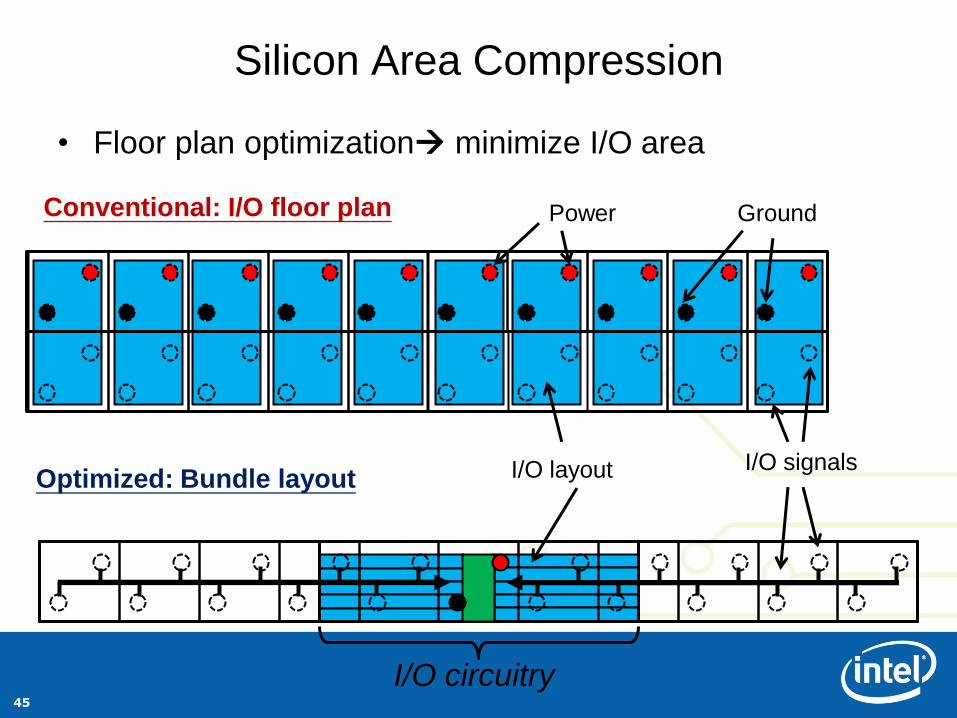
45
Silicon Area Compression
• Floor plan optimization minimize I/O area
Conventional: I/O floor plan Power
I/O layout
Ground
I/O signals
I/O circuitry
Optimized: Bundle layout
46
txbundle_A[0]
rxbundle_A[2]
rxbundle_A[1]
rxbundle_A[0]
txbundle_A[1]
IL-VCO + Drv
Lane[9:5] Lane[4:0]
10 TL pairs
Active I/O circuitry
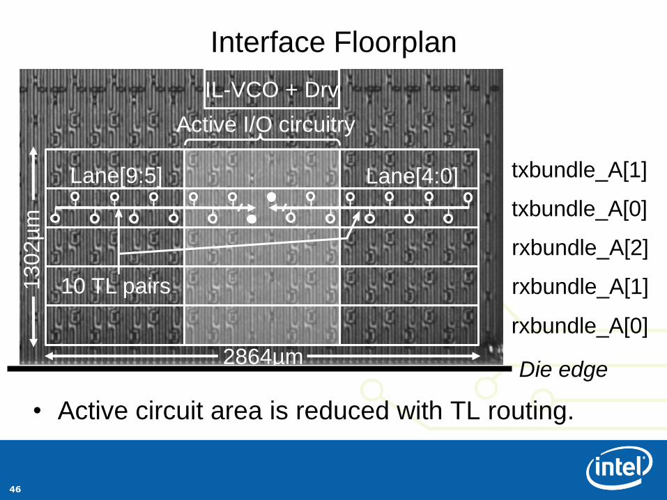
Interface Floorplan1302µ
m
2864µmDie edge
• Active circuit area is reduced with TL routing.

47
Interface Configuration
• Within-bundle lanes matched to <100µm
– Dense LGA connector minimizes breakout area
– Bundles share the same routing layer
– 2X density on stripline layers due to reduced Xtalk
Package
HDI/Flex
bridge500µm LGA
connector
5 signals/mm
Microstrip
Stripline2Stripline1
dieBdieA
SocketPCB

48
Silicon and Interconnect Prototypes
0.5m flex interconnect 3m twinax cable
49
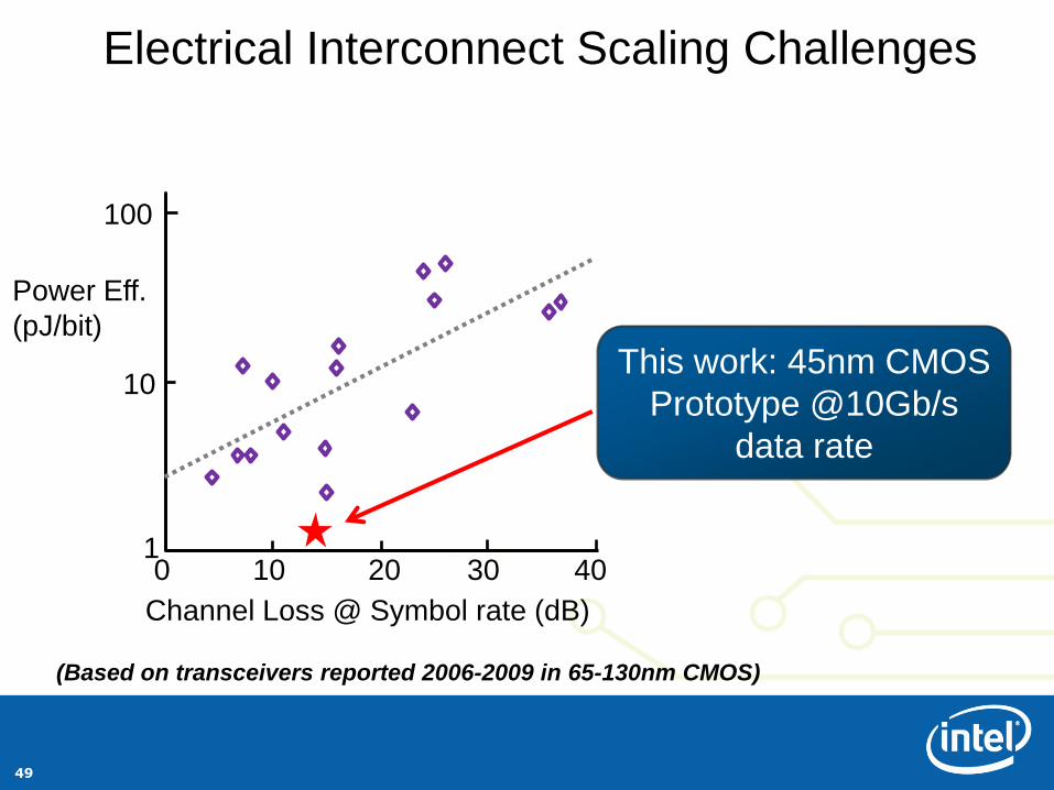
Electrical Interconnect Scaling Challenges
10
100
Power Eff.
(pJ/bit)
0 10 20 30 401
Channel Loss @ Symbol rate (dB)
(Based on transceivers reported 2006-2009 in 65-130nm CMOS)
This work: 45nm CMOS
Prototype @10Gb/s
data rate

50
I/O Power Efficiency Measurements
0.00
0.50
1.00
1.50
2.00
2.50
3.00
0 100 200 300
Po
we
r Ef
fici
en
cy (
pJ/
bit
)
Channel Length (cm)
HDI
LCP flex
32AWG -twinax
Link data rate = 10Gb/s*
*high density
interconnect
(HDI)
51
Summary
• Bandwidth needs are quickly approaching 1TB/s
• Extending electrical I/O to 1TB/s requires balance
between power, data rate, density and cost
• Evaluate alternate channel configurations and
materials
• Recent results indicate that electrical will be up to
the task for “in-box” I/O
51

![Current Affairs 2010_1-Linked [PDF Library]](https://static.fdocuments.in/doc/165x107/552d44684a795970668b46a2/current-affairs-20101-linked-pdf-library.jpg)