The Frequency, Time Design Analysis of Noise Figure ...
8
Communications on Applied Electronics (CAE) – ISSN : 2394-4714 Foundation of Computer Science FCS, New York, USA International Conference on Communication Technology (ICCT 2015) – www.caeaccess.org 35 The Frequency, Time Design Analysis of Noise Figure Optimization of a Wideband PHEMT Hybrid LNA with Flat Gain for WiMAX Application Kishor G. Sawarkar Research Scholar at MCT’s RGIT, Mumbai Pramod K.B. PhD Student of JAIN University Asst Prof. in EXTC Dept. at MCT’s RGIT, Mumbai Kushal Tuckley Director R&D AGV System Mumbai Kumaraswamy H.V. Dept of Telecommunication R. V. C. E, Bangalore, India ABSTRACT In this paper, the Noise figure optimization circuit configuration in PHEMT Hybrid LNA design. The optimal noise figure is achieved by minimizing the noise contributions by utilizing of LC resonance at input and output matching networks to maintain transistor noise optimization.This article as added with not only frequency domain characteristics but also significant time response discussed. Design includes 2 stage cascaded common source PHEMT transistors with inter stage capacitor matching for improvement of gain. An LNA with Bandwidth 2.3-5.8GHz simulation in AWR Microwave office software shows forward gain of 24 dB, noise figure (NF) less than 2 dB and designed amplifier will give the best performance at 5GHz with NF of 0.9 dB and with flat Gain of 24dB. Furthermore, by balun structure input and output time analysis has been done by injecting sinusoidal sample signals with harmonic balance source models. Design is upgraded with EM structure mapping method for accurate results. Keywords Psuedomorphic High electron mobility transistor (PHEMT),Advancing in Wireless Evolution (AWR),Low Noise Amplifier (LNA) and Noise Figure (NF). 1. INTRODUCTION LNA design is a crucial and challenging task at the receiver since received signal will always be weaker in amplitude and corrupted by noise in wireless communications. It should provide low noise figure not only at one frequency but an over range of frequencies or bandwidth of interest [1]. Also requirements of minimum noise figure and maximum gain will always be design trade-offs and cannot be met simultaneously. We need an optimization and fine tuning of component values to get the optimum results. For radio astronomy applications, it is desirable to have wider bandwidth, low noise figure and good gain. There is a trade- off between gain, bandwidth and noise figure (NF). High electron mobility transistor (HEMT) plays a crucial role and is extensively used in ultra-low noise amplifiers 2. A brief Review of existing wideband LNA with noise optimization The key idea of proposed LNA is to get very flat gain throughout the band with minimum noise figure in order to verify and simulating the results AWR Microwave office is used. In this paper [2] SheryAsaadWahbaMarzouk CS topology achieved a high gain but it has tradeoff between gainand matching but CMOS technology offers NF up to 3dB. So for the proposed design as FET technology is used and [3] Ahmed H DC, has tested in microwave the noise performance of GaAs mHEMT and InP pHEMT transistors were presented for both room and cryogenic temperatures by this result the proposed work as done on PHEMT transistor. [4] the inductive peaking technique is used to achieve high and flat value for S21 and good phase linearity is achieved and design include both cascade and cascode. In this paper [5] Pramod K B as simulated the LNA design with I/O matching and intermediate matching network in AWR Microwaveoffice. So proposed work introduced 2 stage cascaded common source PHEMT transistors with I/O matching and capacitive intermediate stage matching networks. 3. Manufacturing Technology, Models and RF Performance Models With the industry's most comprehensive and innovative portfolio of process technologies, E-PHEMT technology with a revolutionary chip scale package Transistor: GaAs pHEMT “ATF36163” from Avago technologies passive fitting to S parameter, EM multiple extraction, normal grounding type. A capacitor of 1pF value of Johansson Company was chosen and resistors of 1kΩ and 150Ω of Panasonic Company were chosen.The use of 0.25-micron gates allows an ultra-low noise figure with respectable associated gain.The PCB board material stack used to qualify the device consists of 40 mil thickness FR4 core material with one-ounce copper for both top and bottom metal. 4. Architecture Circuit design concept DC Port 1 Port 2 Gnd Gnd L1 R1 R2 L2 C2 C1 PHEMT ATF36163 PHEMT ATF36163 Basic Circuit Design Fig 1: Basic circuit design with ideal elements without using micro strip line.
Transcript of The Frequency, Time Design Analysis of Noise Figure ...
Communications on Applied Electronics (CAE) – ISSN : 2394-4714 Foundation of Computer Science FCS, New York, USA International Conference on Communication Technology (ICCT 2015) – www.caeaccess.org
35
The Frequency, Time Design Analysis of Noise Figure
Optimization of a Wideband PHEMT Hybrid LNA with Flat
Gain for WiMAX Application
Kishor G. Sawarkar
Research Scholar at
MCT’s RGIT, Mumbai
Pramod K.B.
PhD Student of JAIN
University
Asst Prof. in EXTC Dept.
at
MCT’s RGIT, Mumbai
Kushal Tuckley
Director R&D
AGV System
Mumbai
Kumaraswamy H.V.
Dept of
Telecommunication
R. V. C. E, Bangalore,
India
ABSTRACT In this paper, the Noise figure optimization circuit
configuration in PHEMT Hybrid LNA design. The optimal
noise figure is achieved by minimizing the noise contributions
by utilizing of LC resonance at input and output matching
networks to maintain transistor noise optimization.This article
as added with not only frequency domain characteristics but
also significant time response discussed. Design includes 2
stage cascaded common source PHEMT transistors with inter
stage capacitor matching for improvement of gain. An LNA
with Bandwidth 2.3-5.8GHz simulation in AWR Microwave
office software shows forward gain of 24 dB, noise figure
(NF) less than 2 dB and designed amplifier will give the best
performance at 5GHz with NF of 0.9 dB and with flat Gain of
24dB. Furthermore, by balun structure input and output time
analysis has been done by injecting sinusoidal sample signals
with harmonic balance source models. Design is upgraded
with EM structure mapping method for accurate results.
Keywords
Psuedomorphic High electron mobility transistor
(PHEMT),Advancing in Wireless Evolution (AWR),Low
Noise Amplifier (LNA) and Noise Figure (NF).
1. INTRODUCTION LNA design is a crucial and challenging task at the receiver
since received signal will always be weaker in amplitude and
corrupted by noise in wireless communications. It should
provide low noise figure not only at one frequency but an over
range of frequencies or bandwidth of interest [1]. Also
requirements of minimum noise figure and maximum gain
will always be design trade-offs and cannot be met
simultaneously. We need an optimization and fine tuning of
component values to get the optimum results. For radio
astronomy applications, it is desirable to have wider
bandwidth, low noise figure and good gain. There is a trade-
off between gain, bandwidth and noise figure (NF). High
electron mobility transistor (HEMT) plays a crucial role and is
extensively used in ultra-low noise amplifiers
2. A brief Review of existing wideband
LNA with noise optimization The key idea of proposed LNA is to get very flat gain
throughout the band with minimum noise figure in order to
verify and simulating the results AWR Microwave office is
used. In this paper [2] SheryAsaadWahbaMarzouk CS
topology achieved a high gain but it has tradeoff between
gainand matching but CMOS technology offers NF up to 3dB.
So for the proposed design as FET technology is used and [3]
Ahmed H DC, has tested in microwave the noise performance
of GaAs mHEMT and InP pHEMT transistors were presented
for both room and cryogenic temperatures by this result the
proposed work as done on PHEMT transistor. [4] the
inductive peaking technique is used to achieve high and flat
value for S21 and good phase linearity is achieved and design
include both cascade and cascode. In this paper [5] Pramod K
B as simulated the LNA design with I/O matching and
intermediate matching network in AWR Microwaveoffice. So
proposed work introduced 2 stage cascaded common source
PHEMT transistors with I/O matching and capacitive
intermediate stage matching networks.
3. Manufacturing Technology, Models and
RF Performance Models With the industry's most comprehensive and innovative
portfolio of process technologies, E-PHEMT technology with
a revolutionary chip scale package Transistor: GaAs pHEMT
“ATF36163” from Avago technologies passive fitting to S
parameter, EM multiple extraction, normal grounding type. A
capacitor of 1pF value of Johansson Company was chosen
and resistors of 1kΩ and 150Ω of Panasonic Company were
chosen.The use of 0.25-micron gates allows an ultra-low noise
figure with respectable associated gain.The PCB board
material stack used to qualify the device consists of 40 mil
thickness FR4 core material with one-ounce copper for both
top and bottom metal.
4. Architecture Circuit design concept
DC
Port 1Port 2
Gnd
Gnd
L1
R1 R2
L2C2
C1
PHEMT ATF36163
PHEMT ATF36163
Basic Circuit Design
Fig 1: Basic circuit design with ideal elements without
using micro strip line.

Communications on Applied Electronics (CAE) – ISSN : 2394-4714 Foundation of Computer Science FCS, New York, USA International Conference on Communication Technology (ICCT 2015) – www.caeaccess.org
36
L1
C1
Cgd1
Cgs1
Gm1*VGS1
Cds1 R1
C2 Cgd2 Cds2
Cgs2 R2
L2
RFout RF in
Gm2*VGS2
Equivalent Circuit
Fig 2: Circuit with necessary PHEMT model for realization.
𝒁𝒊𝒏 = 𝑺𝑳𝟏 + 𝟏
𝑺𝑪𝒊𝒏 (1)
𝑪𝒊𝒏 = 𝑪𝟏 + 𝑪𝒈𝒔𝟏 + 𝑪𝒈𝒅 𝟏 − 𝑨𝒗 (𝟐)
Gain equations with respect to 2 stages
𝑨𝒗 = 𝑨𝒗𝟏 ∗ 𝑨𝒗𝟐 (𝟑)
𝑨𝒗𝟏 = 𝒈𝒎∗𝟏𝒁𝑳𝟏 (𝟒)
𝑨𝒗𝟐 = 𝒈𝒎∗𝟐𝒁𝑳𝟐 (𝟓)
𝒈𝒎∗ = 𝒈𝒎𝒆−𝒊𝝎𝝉 (𝟔)
𝝉 =𝑪𝒈
𝒈𝒎 (7)
𝒈𝒎 = ∈𝒓. 𝑽𝒆𝒇𝒇
𝒅𝒆𝒇𝒇 . 𝒘𝒈 .
𝟏
𝟏 + (𝒏𝒄
𝒏𝒔𝒉𝒆𝒆𝒕)𝟐
(𝟖)
Where,
𝒈𝒎= transconductance
∈𝒓 is the relative dielectric constant
𝑽𝒆𝒇𝒇the effective carrier velocity, 𝒘𝒈 the gate width,
𝒅𝒆𝒇𝒇 an effective gate-to-channel separation
𝒏𝒔𝒉𝒆𝒆𝒕 is the sheet charge density and
𝒏𝒄a reference sheet concentration defined as:
𝒏𝒄 = 𝑬𝒄𝒓𝒊𝒕 .𝒍𝒈.𝑪𝟎
𝒒 (9)
𝑬𝒄𝒓𝒊𝒕 is a critical field for the onset of a "saturated" behavior
and 𝑪𝟎 is an effective channel capacity assuming a fixed
distance between channel charge and gate in a simple
capacitor model.
5. LNA Simulation with Vendor
Components
5.1 Single Transistor The stability factors of the transistor ATF-36163 given by
figure below were found out in the frequency range of 2.3
GHz to 5.8 GHz.
Fig 3: ATF-36163 transistor model
Fig 4: Stability graph of ATF-36163 transistor
The transistor is found to be unstable and gain of the transistor
is varying from 13 dB to 12 dB in the desired frequency range
but we want to achieve a gain of greater than 20 dB, thus we
have cascaded two transistors.
5.2 Two Transistors in cascade Two transistors, ATF-36163 were connected in cascade as
shown in figure 5, and the forward gain (figure 6), stability
parameters (figure 6) were calculated again in the frequency
range of 2.3 GHz to 5.8 GHz.
Fig 5: Schematic of Two Transistors in Cascade
Fig 6: Results of Two Transistors in Cascade
The forward gain S21 was found out to be greater than 20dB,
but the sub circuit was found to be unstable. Thus it was
necessary to stabilize the sub circuit.

Communications on Applied Electronics (CAE) – ISSN : 2394-4714 Foundation of Computer Science FCS, New York, USA International Conference on Communication Technology (ICCT 2015) – www.caeaccess.org
37
5.3 Stabilized Sub-circuit The schematic of the stabilized sub-circuit (figure 7) is given
below
Fig 7: Stabilized sub-circuit schematic
The stability factors (figure 8), K>1 and β> 0, were satisfied
for the stabilized sub-circuit in the frequency range of 2.3
GHz to 5.8 GHz.
Fig 8: Figure Stability of Stabilized Sub-circuit and Noise
figure of Stabilized Sub-circuit
5.4 DC Biasing One of the major advantages of the enhancement mode
technology is that it allows the designer to be able to dC
ground the source leads and then merely apply a positive
voltage on the gate to set the desired amount of quiescent
drain current Id.
Fig 9: DC Biasing
Applying KVL in the output loop we get the following
equation:
Here VDD =12V and IDDis 10mA, using this values we get the
value of RD as 1KΩ.
5.5 Intermediate LNA Schematic After obtaining the biased sub-circuit, the micro-strip lines are
added to connect the lumped elements. Following micro strip
lines were then added: “Mlins", “Mtees", “Mtaper" etc.After
adding micro strip lines, the ideal capacitors and resistors
were replacedwith industry available components.
Fig 10: The final intermediate schematic design
The substrate with εr=12.9 was selected. As we go on
increasing the permittivity of the substrate the thickness of the
substrate goes on decreasing without causing any
complications in the functioning of the circuitry.

Communications on Applied Electronics (CAE) – ISSN : 2394-4714 Foundation of Computer Science FCS, New York, USA International Conference on Communication Technology (ICCT 2015) – www.caeaccess.org
38
Fig 11: Noise Figure of Intermediate LNA
The DC current (IDS) and DC voltage (VDS) are as follows:
Fig 12: DC Current and Voltages
6. Matching Networks The techniques for impedance matching an enhancement
mode device are very similar to those for matching a depletion
mode device. The matching network (figure 13) consists of
matching networks at input and output ends of the
intermediate circuit.
Fig 13: Matching network
The matching equations are,
6.1 Input Matching For input matching, in general the block before LNA either
antenna or filters which is connected will have standard
characteristics of 50Ω output resistance. In order to lower the
system noise and to ensure the maximum power transfer
should have zero reactance.
The source gain circle equations are:
Where,
Cgs= center of the source gain circle
Rgs = radius of the source gain circle
The noise circle equations are:
Where,
CF = center of the noise circle
RF= radius of the noise circle
Fig 14: Schematic of Input Matching Network
6.2 Output Matching For output matching,
The load gain circle equations are:
Where,
CgL= center of the load gain circle
RgL = radius of the load gain circle
Communications on Applied Electronics (CAE) – ISSN : 2394-4714 Foundation of Computer Science FCS, New York, USA International Conference on Communication Technology (ICCT 2015) – www.caeaccess.org
39
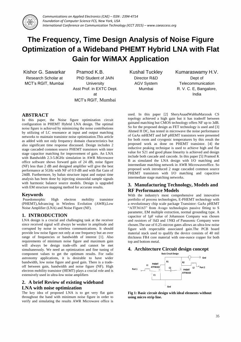
Fig 15: Schematic of Output Matching network
Fig 16: 2D View of LNA
Fig 18: 3D View of LNA
The red cylinders are vias. The green components are lumped
circuit elements. The yellow patches are copper patches
7. Complete LNA Design After combining Input Matching circuit, Intermediate sub-
circuit and Output Matching circuit into a single circuit, the
low noise amplifier was designed.
Fig 17: Schematic of Complete Low Noise Amplifier
7.1 Development of Layout Layout is facet of the LNA design work will all vendor
components is complete and errors have been successfully
removed with the additional steps process: Extraction, Layout
Versus Schematic (LVS) Check, and Post-Layout
Simulations. Extraction involves the creation of a circuit
description called a netlist which provides information
regarding the transistors and their interconnections. The
circuit is terminated with a 50Ω port on the input and output
side. The circuit is named LNA
8. Simulation Results and Analysis
8.1 The forward gain (S21)
Fig 19: Forward gain response of the complete circuit. The forward gain (S21) of the LNA varies from 23.89 dB to
24.46 dB in the frequency range of 2.3 GHz to 5.8 GHz while
providing a flatness of 0.57dB. The forward gain takes a
maximum value of 24.46 dB at 3 GHz and is considerably
high at 4 GHz and 5 GHz.
Communications on Applied Electronics (CAE) – ISSN : 2394-4714 Foundation of Computer Science FCS, New York, USA International Conference on Communication Technology (ICCT 2015) – www.caeaccess.org
40
8.2 Noise Figure (NF)
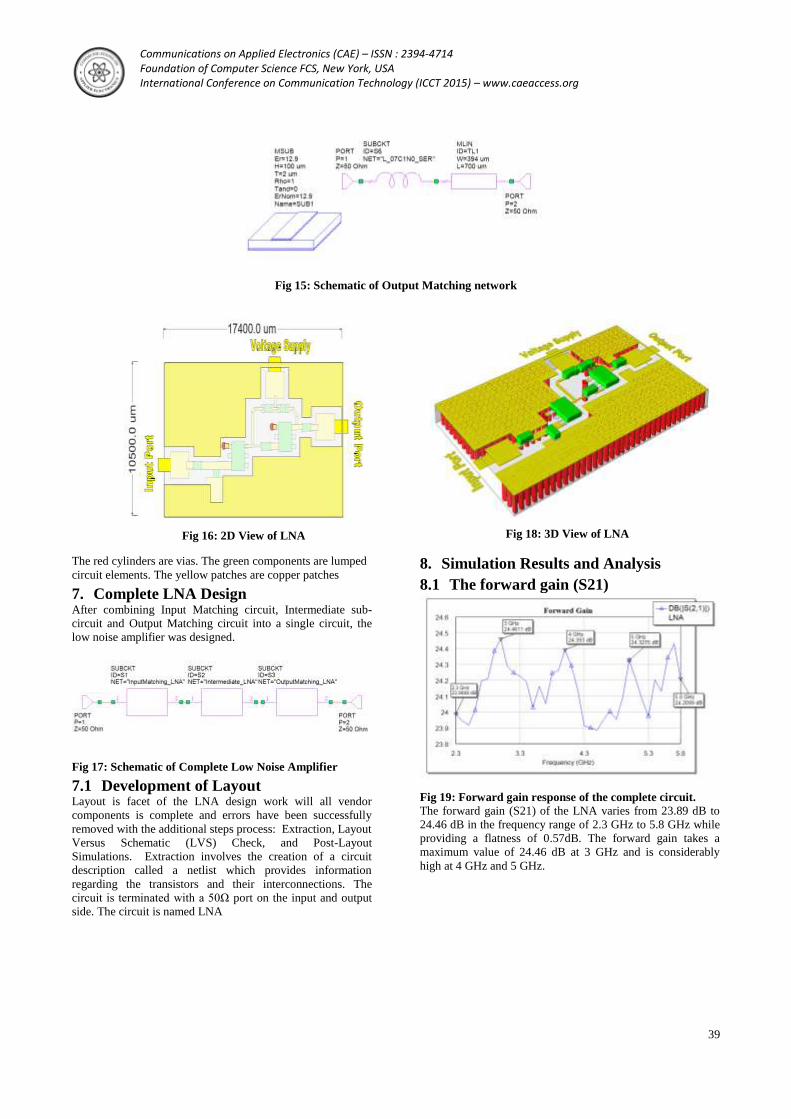
Fig 20: Noise figure response of the complete circuit.
The noise figure (NF) goes on decreasing with the increase in
frequency from 1.56 dB at 2.3 GHz to 1.02 dB at 5.8 GHz,
and has the minimum value of 0.96 dB at 5 GHz. The
minimum noise figure goes on increasing as the frequency
increases from 0.63 dB at 2.3 GHz to 0.81 dB at 5.8 GHz.
8.3 Return Loss
Fig 21: Return loss of the complete LNA circuit.
The input return loss S11 is less than 0 dB throughout the
frequency range of 2.3 GHz to 5.8 GHz and is minimum at 5
GHz with -11.96 dB value. The output return loss S22 is less
than 0 dB throughout the frequency range of 2.3 GHz to 5.8
GHz and is minimum at around 5 GHz with -13.02 dB value.
8.4 VSWR Limitation
Fig 22: VSWR at Input and Output of the complete LNA
circuit.
Design shows very good response at 4.8GHz at input side 1.6
and output side 1.5GHz and there is small limitation at the
input since its value is more at lower frequency and optimum
value after 3.5 GHz.
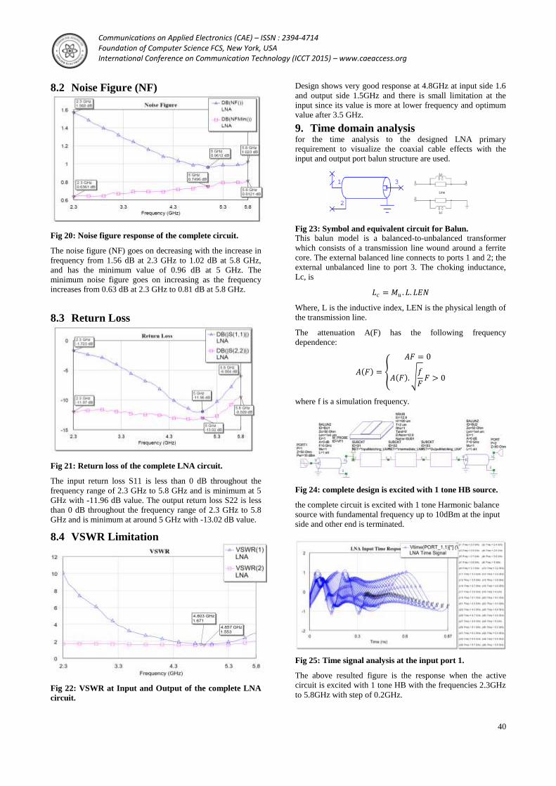
9. Time domain analysis for the time analysis to the designed LNA primary
requirement to visualize the coaxial cable effects with the
input and output port balun structure are used.
Fig 23: Symbol and equivalent circuit for Balun.
This balun model is a balanced-to-unbalanced transformer
which consists of a transmission line wound around a ferrite
core. The external balanced line connects to ports 1 and 2; the
external unbalanced line to port 3. The choking inductance,
Lc, is
𝐿𝑐 = 𝑀𝑢 . 𝐿. 𝐿𝐸𝑁
Where, L is the inductive index, LEN is the physical length of
the transmission line.
The attenuation A(F) has the following frequency
dependence:
𝐴 𝐹 =
𝐴𝐹 = 0
𝐴 𝐹 . 𝑓
𝐹𝐹 > 0
where f is a simulation frequency.
Fig 24: complete design is excited with 1 tone HB source.
the complete circuit is excited with 1 tone Harmonic balance
source with fundamental frequency up to 10dBm at the input
side and other end is terminated.
Fig 25: Time signal analysis at the input port 1.
The above resulted figure is the response when the active
circuit is excited with 1 tone HB with the frequencies 2.3GHz
to 5.8GHz with step of 0.2GHz.

Communications on Applied Electronics (CAE) – ISSN : 2394-4714 Foundation of Computer Science FCS, New York, USA International Conference on Communication Technology (ICCT 2015) – www.caeaccess.org
41
Fig 26: Time signal analysis at the output port 2.
The above resulted response is found when the active circuit
is excited for the active termination that applies load
impedance Z(50Ω) while supplying a power signal of
magnitude power and angleswept across the band (2.3GHz to
5.8GHz).
Fig 27: Showing EM structure line type with EM Mapping
layout.
The design is updated to EM structure line type with EM
mapping which uses both physical properties and conduction
properties in stack up. it has been re-simulated for the entire
frequency band. Each and every sub block have been updated
with new interpolation data and extrapolation was not possible
for this design.
10. Conclusion At the system level, receiver sensitivity is dominated by the
noise figure, Gain and linearity so in this paper a two stage
LNA is designed by adding an input and output matching
Network and DC bias, its behavior is carefully analyzed in
AWR Microwave office. An algorithmic design methodology
for simultaneous noise and input/output impedance matching
in Microwave LNAs has been presented and verified. The
results achieved in this work is having I/O matching network
which is evaluated and relative performance is compared with
below mentioned papers in terms of bandwidth, forward gain
and noise figure.
Table 1. Comparison between proposed work and related
recent published work
Reference Bandwidth
(GHz)
Noise
Figure (dB)
Gain
(dB)
[6] Single point at 1 0.6 17.49
[1] 2-11 1.6-4 15
[7] Single point 2.4 1.8 12.09
[8] 2.1-2.5 1.9-2.1 11.9
This work 2.3-5.8 <1.5 24
This work 5 0.9 24
Thus, the designed amplifier has claims the advantages of
better matching network yields a Forward flat gain of 24 dB
Noise figure less than 1.6 dB over the bandwidth from 2.3
GHz to 5.8 GHz with high linearity and stability. The design
shows the best performance at 5GHz providing the Gain 24dB
and limiting the Noise figure to 0.9dB. The design is
thoroughly measured by using harmonic balance models.
Time analysis has been executed at both input and output
ports with 1 tone analysis. For time analysis the excited tone
has been varied from 2.3GHz to 5.8GHz with RF input up to
10dBm. The design has got very compromising response with
sinusoidal signal and also in turn promising for random
signals too. Design is upgraded with EM Structure mapping
which is very much required for all microwave device which
operates more than 2GHz.
11. Future scope In future multilevel interconnects to realize vertically
integrated RF, Microwave MMIC technology is expected to
use the current Hybrid technology design. So this work as
opened numerous area for future work with respect to flat gain
response in LNA design which could be done better
understanding for the LNA measurements in the receiver
system. The shown 3-D layout technology and EM Structure
mapping is promising in performance of fabrication. Same
deign can be upgraded to MMIC design by using Industrial
standard process development kit.The MMIC fabrication
techniques are diffusion, ion plantation and epitaxial growth
etc. required this kind of work on basic hybrid MIC
technology.In addition to this work followed by the
fabrication by using MMIC technology and will be integrated
to the receiver system of some of the applications like
WiMAX, Digital Audio Radio Satellite (DARS), Amateur
radio, Airport surveillance radars and S/C band radars. Also
commercially viable wireless application in huge scale.
12. ACKNOWLEDGMENTS This work is supported by MCT's Rajiv Gandhi Institute of
Technology, Mumbai and also authors would like to thank Dr.
UdhavBhosle, Principal of RGIT, Chairman, Board of Studies
in EXTC Engineering, University of Mumbai for significant
support and encouragement for this research work. The
authors would like to special thanks forDr. Krishna
Venkatesh, Director & Chief Technological Officer, Jain
University, Prof. K. T Srirangaraj , Dr. TGS Moorthy, Prof.
Chandrashekar K. CET, Jain University, Bangalore and Mr.
Manjunatha Reddy H. V Technical Manager, RF and μW
division, Icon Design Automation Pvt. Ltd. for their valuable
guidance.
13. REFERENCES [1] Niti Mohan, Vaithianathan.V “Noise Analysis of the
Input Matching Circuits for UWB Low Noise
Amplifiers” at International conference on
Communication and Signal Processing, April 3-5, 2013,
India , 978-1-4673-4866-9/13/$31.00 ©2013 IEEE Pg :
545- 550
[2] SheryAsaadWahbaMarzouk, Faisal A. Hussien, A. M.
Shousha “A 3dB NF 0.1–6.6GHzInductorlessWideBand
Low Noise Amplifier in 0.13µm CMOS”978-1-4799-
4132-2/14/$31.00 ©2014 IEEE Pg : 953- 956
[3] Ahmed H. Akgiray, Sander Weinreb, Rémy Leblanc,
Michel Renvoise, Peter Frijlink, Richard Lai, and
Stephen Sarkozy, “Noise Measurements of Discrete
HEMT Transistors and Application to Wideband
VeryLow-Noise Amplifiers”IEEE TRANSACTIONS

Communications on Applied Electronics (CAE) – ISSN : 2394-4714 Foundation of Computer Science FCS, New York, USA International Conference on Communication Technology (ICCT 2015) – www.caeaccess.org
42
ON MICROWAVE THEORY AND TECHNIQUES,
VOL. 61, NO. 9, SEPTEMBER 2013Pg : 3285-3297
[4] A.P. Adsul, Dr. S.K. Bodhe, “A Low-Noise Amplifier
Design for 3.1-10.6 GHz Impulse Radio Ultra Wideband
Receivers.” 978-1-4673-5090-7/13/$31.00 ©2013 IEEE
Pg: 470-474
[5] Pramod K B, Kumaraswamy H.V, Praveen K B, “The
Design and Simulation of Radio Frequency Narrow Band
Low Noise Amplifier with Input, Output, Intermediate
Matching” 978-1-4799-0400-6/13/$31.00 ©2013 IEEE
[6] J.Manjula, S.Malarvizhi, “A 1GHz Current Reuse Low
Noise Amplifier with Active Inductor Load” 978-1-
4673-5090-7/13/$31.00 ©2013 IEEE Pg: 211-215
[7] Fan Cai, A. ÇarUlusoy, John Papapolymerou , “2.4 GHz
Low Cost Low Noise Amplifier on Flexible Organic
Substrate” 2013 Asia-Pacific Microwave Conference
Proceedings , 978-1-4799-1472-2/13/$31.00 ©2013
IEEE Pg: 270-272
[8] YANG Zong-shuai ,Niehai ,HAN Wen-tao , “A high-
linearity S-band SiGe HBT low-noise amplifier
design”2013 International Workshop on Microwave and
Millimeter Wave Circuits and System Technology , 978-
1-4673-5504-9/13/$31.00 ©20 13 IE E EPg: 308-311
[9] IoanaGiangu , Valentin Buiculescu, “Broadband Two
Stages Low Noise Amplifier for Milimeter Wave” 978-
1-4673-5672-5/13/$31.00 © 2013 IEEE Pg: 323-326
[10] FarzanehTaringou, Jens Bornemann, KeWu, “Broadband
coplanar-waveguide and microstriplow-noise amplifier
hybrid integrations for K-band substrate integrated
waveguide applications on low-permittivity
substrate”IET Microw. Antennas Propag., 2014, Vol. 8,
Iss. 2, pp. 99–103doi: 10.1049/iet-map.2013.0251
[11] M. A. Bashir, M. M. Ahmed, U. Rafique, Q. D. Memon
“Design of a Ku Band High Gain Low Noise Amplifier”
2013 IEEE International RF and Microwave Conference
(RFM2013), December 09-11, 2013 - Penang, Malaysia
978-1-4799-2214-7/13/$31.00 ©2013 IEEE Pg : 168-171
[12] T Kawasaki', M Kubota', K. Tsukashima', T Tokumitsu',
and Y Hasegawa “A Full E-band Low Noise Amplifier
Realized by Using Novel Wafer-Level Chip Size
Package Technology Suitable for Reliable Flip-chip
Reflow-Soldering” 978·1-4799-3869-8'14/$31.00 ®2014
IEEE.
[13] Kishor G Sawarkar, Pramod K B Tuckley and
KumaraswamyH.v. Article: Design and Analysis of
Noise Figure Optimization of a wideband PHEMT
Hybrid LNA with Flat gain for WiMAX
Application. IJCA Proceedings on International
Conference on Computer Technology ICCT 2015(7):10-
16, September 2015.
14. AUTHOR PROFILE Mr. Pramod K B was born in Mysore, Karnataka, India in
1989. He is currently working as Assistant Professor in
MCT’s RGIT, Mumbai and also working towards PhD degree
at JAIN University, Bangalore in Electronics Engineering. He
received his B.E degree in Electronics and Communication
from Dr.Ambedkar Institute of Technology, Bangalore
Visvesvaraya Technological University in 2010, M.Tech
degree in R F Communication from Jain University,
Bangalore, in 2012 and He worked as R F Design trainee at
Icon Design and Automation Pvt LtD and as visiting research
scholar at University of Concordia, Montreal, Quebec,
Canada. His research includes Design, Characterization And
Optimization Of RF Passive Devices , Board Level Tuning
And Optimization Of Matching Networks, Low Noise
Amplifier , Power Amplifier, Circuit Linearization And High-
Efficiency Design Techniques, Circuit Instability And
Strategies.
K. G. Sawarkar is currently working as head of electronics &
telecommunication enggDept. RGIT, Mumbai and Research
Scholar in Mumbai University. His Area of Interest is Design
of analog circuits , design of RF circuits and systems He has
done his BE in Electronics and telecommunication under
Amravati University and M.E from Mumbai University.
Prof. Dr. KumaraswamyH.V is currently working as
Professor & HOD in the Dept of Telecommunication
Engineering, RVCE, and Bangalore. His research interests are
Digital Signal Processing, Adaptive Signal Processing and
Communication. He has got PhD from Visvesvaraya
Technological University for the research work on Smart
Antenna System using Dielectric lens. He is the author of the
book titled "Signals & Systems" Published by: SciTech
Publication, Chennai, ISB No.8188429260.
Dr. Kushal R. Tuckley is currently working as Chairman.
Head, R&D, agv systems pvt ltd. Mumbai.He is an expert in
the field of DSP, Radars and RF/Microwave systems. He has
B. Tech, M.Tech and PhD from IIT Bombay. He had a 25
year long career as a scientist in Society for Applied
Microwave Electronics Engineering and Research
(SAMEER), a premium research institute in microwave
systems engineering. He has significant contribution in many
of the prestigious projects commissioned by the Govt. of
India. He had a stint at Astra Microwave Products Ltd
E-mail: [email protected]