THE FLORIDA STATE UNIVERSITY COLLEGE OF ENGINEERING DESIGN...
73
THE FLORIDA STATE UNIVERSITY COLLEGE OF ENGINEERING DESIGN OF A COMPACT MICROSTRIP PATCH ANTENNA FOR USE IN WIRELESS/CELLULAR DEVICES By: Punit S. Nakar A Thesis submitted to the Department of Electrical And Computer Engineering in partial fulfillment of the requirements for the degree of Master of Science Degree awarded: Spring semester, 2004
Transcript of THE FLORIDA STATE UNIVERSITY COLLEGE OF ENGINEERING DESIGN...

THE FLORIDA STATE UNIVERSITY
COLLEGE OF ENGINEERING
DESIGN OF A COMPACT MICROSTRIP PATCH ANTENNA FOR USE IN
WIRELESS/CELLULAR DEVICES
By:
Punit S. Nakar
A Thesis submitted to the Department of Electrical And Computer Engineering
in partial fulfillment of the requirements for the degree of
Master of Science
Degree awarded: Spring semester, 2004

ii
The members of the committee approve the thesis of Punit S. Nakar defended on March 4, 2004.
_____________________ Dr. Frank Gross,
Professor Directing Thesis
_____________________ Dr. Krishna Arora,
Committee member
____________________ Dr. Rodney Roberts, Committee member
Approved: ____________________________________________ Dr. Reginald Perry, Chair, Department of Electrical and Computer Engineering
____________________________________________ Dr. C.J. Chen, Dean, FAMU-FSU College of Engineering
The Office of Graduate Studies has verified and approved the above named committee members.

iii
To my family

iv
ACKNOWLEDGEMENTS I wish to express sincere gratitude to my supervisor Dr. Frank B. Gross for providing me
an opportunity to work in the Sensor Systems Research Lab. His invaluable guidance and
support have added a great deal to the substance of this thesis, and taught me an enormous
amount in the process. Dr. Gross patiently went over the drafts suggesting numerous
improvements and constantly motivated me in my work. I must also thank my committee
members Dr. Krishna Arora and Dr. Rodney Roberts for encouraging my academic and research
efforts. A special thanks to Dr. Roberts for allowing me access to his research laboratory for
carrying out some simulations for this thesis.
Besides professors, my friends here at FSU have also given me crucial assistance and
fruitful suggestions in my research and academic coursework. I would like to thank them as well
for the relaxing discussions I had with them.
Last but not least, a very big thank you to my beloved family and my future wife-to-be
for their support, love and constant encouragement they have bestowed upon me. Without their
support, I would never have gotten so far.

v
TABLE OF CONTENTS
List of Tables……………………………………………………………………………………..vi List of Figures………………………................…………………………………………………vii Abstract……………………………………………………………………………………………x 1. Background of Wireless Communications…………….….……………………………………1 1.1 Cellular Systems – The past…………………………………………………………...1 1.2 Cellular Systems – The present………………………………………………………..3 1.3 Cellular Systems – Vision of the future……………………………………………….3 1.4 Inside a Cellular Phone………………………………………………………………..5 2. Antenna Fundamentals…...…………………….……….…………………………………….. .9
2.1 Introduction…………………………………………………………………………....9 2.2 How an Antenna radiates...…………………………………………………………....9 2.3 Near and Far field regions…………………………………………………………....11 2.4 Far field radiation from wires………………………………………………………..12 2.5 Antenna performance parameters……………………………………………………14 2.6 Types of Antennas…………………………………………………………………...23
3. Microstrip Patch Antenna...………………………………….………………………………..31 3.1 Introduction……………...………………………….………………………………..31 3.2 Advantages and Disadvantages……. ………………………………………………..32 3.3 Feed Techniques………... …………………………………………………………..34 3.4 Methods of Analysis…………………………. ………….………………………….38
4. Microstrip Patch Antenna Design and Results………………………………………………..48 4.1 Design Specifications……………………………………………………………......48 4.2 Design Procedure......………………………………………………………………...49 4.3 Simulation Setup and Results………………………………...……………………...52
5. Conclusions………………………………………………………………………..…………..59 REFERENCES……………………………………………………………….……...…………..61 BIOGRAPHICAL SKETCH………………………………….………………………….......….63

vi
LIST OF TABLES
1. Table 3.1 Comparing the different feed techniques…..…………………..…………...38 2. Table 4.1 Effect of feed location on center frequency, return loss and bandwidth…...53

vii
LIST OF FIGURES
1. Figure 1.1 Frequency Reuse pattern.....…………………………………………………....…...2 2. Figure 1.2 Cell structure for PCS…....……………………………………………...…………..3 3. Figure 1.3 The future vision…………………………………………………………………….4 4. Figure 1.4 User at home, in car, at office, at business trip..…………………………………….5 5. Figure 1.5 Internal components of a NOKIA cellular phone…..……………………………….6 6. Figure 1.6 Cellular handset used with the AMPS system…………………………....................7 7. Figure 1.7 Cellular handsets used in the past few years………………………………………..7 8. Figure 2.1 Radiation from an antenna…………………………………………….…………...10 9. Figure 2.2 Field regions around an antenna……...…………………………………................11 10. Figure 2.3 Spherical co-ordinate system for a Hertzian dipole……………………………...12 11. Figure 2.4 Radiation pattern of a generic directional antenna……………………………….15 12. Figure 2.5 Equivalent circuit of transmitting antenna………………………….....................17 13. Figure 2.6 A linearly (vertically) polarized wave……………………………………………20 14. Figure 2.7 Commonly used polarization schemes…………………………………………...21 15. Figure 2.8 Measuring bandwidth from the plot of the reflection coefficient………………...22 16. Figure 2.9 Half wave dipole………………………………………………………………….23

viii
17. Figure 2.10 Radiation pattern for Half wave dipole……………………………...………….24 18. Figure 2.11 Monopole Antenna……………………………………………………………...24 19. Figure 2.12 Radiation pattern for the Monopole Antenna…………………………………...25 20. Figure 2.13 Loop Antenna…………………….......................................................................26 21. Figure 2.14 Radiation Pattern of Small and Large Loop Antenna..…………………………26 22. Figure 2.15 Helix Antenna…………………………………………………………………...27 23. Figure 2.16 Radiation Pattern of Helix Antenna………………………………..…………...28 24. Figure 2.17 Types of Horn Antenna………………………………………………................29 25. Figure 3.1 Structure of a Microstrip Patch Antenna……………………...………………….31 26. Figure 3.2 Common shapes of microstrip patch elements…………………………………...32 27. Figure 3.3 Microstrip Line Feed…………………………………………………………..…34 28. Figure 3.4 Probe fed Rectangular Microstrip Patch Antenna………………………………..35 29. Figure 3.5 Aperture-coupled feed……………………………………………………………36 30. Figure 3.6 Proximity-coupled Feed……………………………………………….................37 31. Figure 3.7 Microstrip Line ………………..............................................................................39 32. Figure 3.8 Electric Field Lines ………………………………………………………………39 33. Figure 3.9 Microstrip Patch Antenna………………………………………………………...40 34. Figure 3.10 Top View of Antenna …………………………………………………………..41 35. Figure 3.11 Side View of Antenna ……………………...…………………………………..41 36. Figure 3.12 Charge distribution and current density creation on the microstrip patch…...….43 37. Figure 4.1 Top view of Microstrip Patch Antenna………………………………..…………49 38. Figure 4.2 Microstrip patch antenna designed using IE3D …………….……………………52 39. Figure 4.3 Return loss for feed located at different locations……………………..…………54

ix
40. Figure 4.4 Return loss for feed located at (4, 0)……………………………………………..55 41. Figure 4.5 Elevation Pattern for φ = 0 and φ = 90 degrees………….…………………….56 42. Figure 4.6a 3D view of radiation pattern looking along the Y axis in the XZ plane...............57 43. Figure 4.6b 3D view of radiation pattern looking along the Z axis in the XY plane………..57 44. Figure 4.7a 3D view of radiation pattern for cellular phone orientation in the YZ plane..….57 45. Figure 4.7b 3D view of radiation pattern for cellular phone orientation in the XZ plane…...57

x
ABSTRACT The cellular industry came into existence 25 years ago and as of today, there are
approximately 150 million subscribers worldwide. The cellular industry generates $30 billion in
annual revenues and is one of the fastest growing industries. The cellular handsets being used in
the 1980s were bulky and heavy. Advancements in VLSI technology have enabled size reduction
for the various microprocessors and signal processing chips being used in cellular phones.
Another method for reducing handset size is by using more compact antennas. The aim of this
thesis is to design such a compact antenna for use in wireless/cellular devices.
A Microstrip Patch Antenna consists of a dielectric substrate on one side of a patch, with
a ground plane on the other side. Due to its advantages such as low weight and volume, low
profile planar configuration, low fabrication costs and capability to integrate with microwave
integrated circuits (MICs), the microstrip patch antenna is very well suited for applications such
as cellular phones, pagers, missile systems, and satellite communications systems. A compact
microstrip patch antenna is designed for use in a cellular phone at 1.9 GHz. The results obtained
provide a workable antenna design for incorporation in a cellular phone.

61
REFERENCES [1] Rappaport, Theodore S., Wireless Communications: Principles and Practice, Prentice Hall Communications Engineering and Emerging Technologies Series, 1999. [2] www.wirelessadvisor.com [3] http://web.bham.ac.uk/eee1roj8/websites_demo [4] Stutzman, W.L. and Thiele, G.A., Antenna Theory and Design, John Wiley & Sons, Inc, 1998. [5] Balanis, C.A., Antenna Theory: Analysis and Design, John Wiley & Sons, Inc, 1997. [6] Makarov, S.N., Antenna and EM Modeling with MATLAB, John Wiley & Sons, Inc, 2002. [7] Ulaby, F.T., Fundamentals of Applied Electromagnetics, Prentice Hall, 1999. [8] Saunders, S.R., Antennas and Propagation for Wireless Communication Systems, John Wiley & Sons, Ltd, 1999. [9] Kumar, G. and Ray, K.P., Broadband Microstrip Antennas, Artech House, Inc, 2003. [10] Garg, R., Bhartia, P., Bahl, I., Ittipiboon, A., Microstrip Antenna Design Handbook, Artech House, Inc, 2001. [11] Qian, Y., et al., “A Microstrip Patch Antenna using novel photonic bandgap structures”, Microwave J., Vol 42, Jan 1999, pp. 66-76. [12] Balanis, C.A., Advanced Engineering Electromagnetics, John Wiley & Sons, New York, 1989

62
[13] Hammerstad, E.O., “Equations for Microstrip Circuit Design,” Proc. Fifth European Microwave Conf., pp. 268-272, September 1975. [14] James, J.R. and Hall, P.S., Handbook of Microstrip Antennas, Vols 1 and 2, Peter Peregrinus, London, UK, 1989. [15] Bahl, I.J. and Bhartia, P., Microstrip Antennas, Artech House, Dedham, MA, 1980. [16] Richards, W.F., Microstrip Antennas, Chapter 10 in Antenna Handbook: Theory Applications and Design (Y.T. Lo and S.W. Lee, eds.), Van Nostrand Reinhold Co., New York, 1988. [17] Newman, E.H. and Tylyathan, P., “Analysis of Microstrip Antennas Using Moment Methods,” IEEE Trans. Antennas Propag., Vol. AP-29, No. 1, pp. 47-53, January 1981. [18] Harrington. R.F., Field Computation by Moment Methods, Macmillan, New York, 1968. [19] Kantorovich, L. and Akilov, G., Functional Analysis in Normed Spaces, Pergamon, Oxford, pp. 586-587, 1964. [20] IE3D 10.0, Zeland Software Inc., Fremont, CA.

63
BIOGRAPHICAL SKETCH
Punit Shantilal Nakar was born in Mumbai, India on July 29 1979. He received his
Bachelors degree in Electronics and Telecommunications in 2001 from the Bharati Vidyapeeth
College of Engineering (B.V.C.O.E) affiliated with Mumbai University. Feeling the need to
pursue higher education, he enrolled for the Master’s program in Electrical Engineering at the
Florida State University in Fall 2001. He worked part time with different departments at FSU
such as the Communication and Multimedia Services, Department of Meteorology and the
Department of Electrical Engineering as a Graduate Assistant. Apart from academics, his prime
hobbies are music, cricket and reading.

1
CHAPTER 1
BACKGROUND OF WIRELESS COMMUNICATIONS
In 1897, Guglielmo Marconi demonstrated radio’s ability to provide continuous contact
with ships sailing across the English Channel. Since then, numerous advances have been made in
the field of wireless communications. Numerous experiments were carried out by different
researchers to make use of electromagnetic waves to carry information.
1.1 Cellular Systems – The Past
The first public mobile telephone service was launched in the United States in the year
1946. Distances up to 50 km were covered using a single, high-powered transmitter on a large
tower. These services offered only half duplex mode (only one person could talk at a time) and
used 120 kHz of RF bandwidth. Only 3 kHz of baseband spectrum was required but due to
hardware limitations, 120 kHz was used. By the mid 1960s, due to technology advancements, the
bandwidth for voice transmissions was cut down to 30 kHz. By this time, automatic channel
trunking was introduced under the label IMTS (Improved Mobile Telephone Service) which also
offered full duplex service. However, IMTS quickly became saturated since they had few
channels and a very large population to serve as discussed by Rappaport [1].
In the 1960s, the AT&T Bell Laboratories and other telecommunication companies
developed the technique of cellular radiotelephony – the concept of breaking a coverage area into
small cells, each of which reused portions of the spectrum to increase spectrum usage at the
expense of greater system infrastructure. Figure 1.1 shows the concept of frequency reuse. A cell
using frequency 1f has to be located at a particular distance away from another cell using the

2
same frequency to prevent interference. Thus same frequencies would not be used in adjacent
cells. The reuse distance depends on the number of cells forming a cluster which uses all the
available frequencies.
Figure 1.1 Frequency Reuse pattern
The entire spectrum allocated by the FCC was divided into a number of channels and
these channels were used in the cells. Channels would be reused only when there would be
sufficient distance between the transmitters to prevent interference. In 1983, the FCC (Federal
Communications Commission) allocated channels for the AMPS (Advanced Mobile Phone
System) in the range 824-894 MHz. In order to encourage competition and keep prices low, the
U. S. government required the presence of two carriers in every market. Each carrier was
assigned 832 frequencies: 790 for voice and 42 for data. A pair of frequencies (one for transmit
and one for receive) was used to create one channel. The frequencies used in analog voice
channels are typically 30 kHz wide, hence 30 kHz was chosen as the standard size because it
gave voice quality comparable to a wired telephone. The transmit and receive frequencies of
each voice channel were separated by 45 MHz to keep them from interfering with each other.
The AMPS used analog FM along with FDMA [1].
In 1991, the first digital system was installed in major US cities. This system was called
the USDC (U.S. Digital Cellular) and it used digital modulation along with TDMA to give three
times improved capacity. It used the same frequency range as the AMPS, i.e. 824-894 MHz. The
1f2f
3f
4f
5f6f
7f
1f
2f3f
Reuse distance

3
IS-95 was the next digital system launched in 1993 and this used CDMA. It had a channel
bandwidth of 1.25 MHz and used QPSK/BPSK modulation.
1.2 Cellular Systems – The Present
Further improvements and advances in technology led to the PCS (Personal
Communication Services) in 1995. One example of a PCS system is the DCS-1900 which uses
the 1850-1990 MHz band and is in use today. This system is based on TDMA and has 200-kHz
channel spacing and eight time slots. The system also provides services like paging, caller ID,
and e-mail. In a PCS system, the cells are further divided into macrocells, microcells and
picocells to facilitate better coverage as shown in Figure 1.2 (www.ee.washington.edu).
Figure 1.2 Cell structure for PCS
1.3 Cellular Systems – Vision for the Future
According to the Cellular Telecommunications Industry Association (CTIA), today there
exist more than 60 million wireless customers. This figure is hard to imagine considering the fact
that cellular service was invented about 50 years ago. Over the last 25 years, the wireless market

4
has grown steadily from a $3 billion market to a $30 billion market in terms of annual revenues
as indicated by [2].
Figure 1.3 The future vision
Figure 1.3 (www.web.bham.ac.uk) shows the vision of the future. An integrated
terrestrial/satellite multimedia system is envisioned. Global personal communication is to be
supported via satellites using the satellite gateways to connect to the fixed ground network.
Underground cable, optical fibers or fixed radio links would be used to link the gateways to the
fixed networks. The fixed networks would be connected to cellular base stations providing radio
links to mobile hand sets or hand set units on vehicles. Indoor base stations located in offices and
public places such as bus and rail stations, airports and shops would also be connected to the
fixed network. In areas which cannot be provided coverage by terrestrial base stations or fixed
networks, satellites would be used to connect to the personal handsets.

5
Hence, in the future, the handsets would be such that they would support multimedia
which is an integration of voice, data and video signals. Thus, the user would have access to a
very wide range of services such as telephone, fax, electronic mail, world wide web, video
conferencing, remote shopping and emergency services [3].
In the present world cordless, indoor and other types of cellular phones are available for
different applications. In the future, a single handset will be used to serve all applications. The
handset may be used by the user when he is at his home. The same handset would then be
connected to the cellular network when the user would be in his car. When the user reaches his
workplace, the same handset can be connected to the office cordless system. Moreover, on a
business trip, the user would use the handset through the satellite as shown in Figure 1.4 [3].
Figure 1.4 User at home, in car, at office, at business trip
1.4 Inside a Cellular Phone
Cellular phones are some of the most intricate devices people use on a daily basis.
Modern digital cell phones can process millions of calculations per second in order to compress
and decompress the voice stream.
6
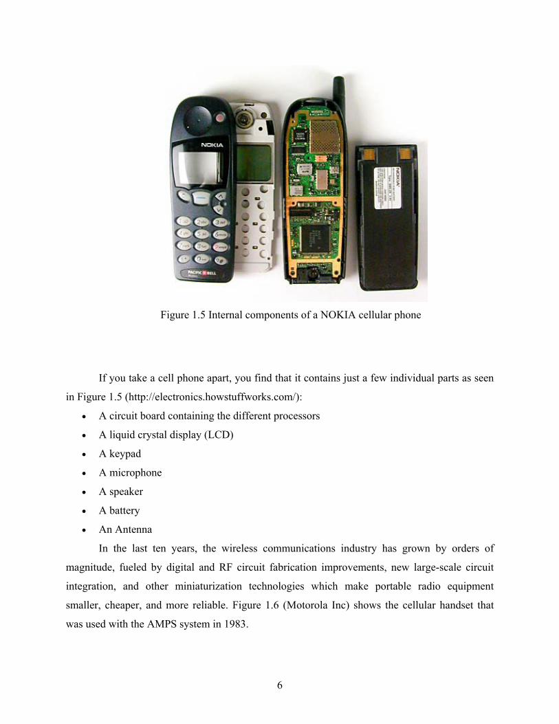
Figure 1.5 Internal components of a NOKIA cellular phone
If you take a cell phone apart, you find that it contains just a few individual parts as seen
in Figure 1.5 (http://electronics.howstuffworks.com/):
• A circuit board containing the different processors
• A liquid crystal display (LCD)
• A keypad
• A microphone
• A speaker
• A battery
• An Antenna
In the last ten years, the wireless communications industry has grown by orders of
magnitude, fueled by digital and RF circuit fabrication improvements, new large-scale circuit
integration, and other miniaturization technologies which make portable radio equipment
smaller, cheaper, and more reliable. Figure 1.6 (Motorola Inc) shows the cellular handset that
was used with the AMPS system in 1983.
7
Figure 1.6 Cellular handset used with the AMPS system
Figure 1.7 (http://www.nttdocomo.co.jp) shows the kind of cellular handsets that were
available in the past and it is seen that over a period of years, the handsets are becoming smaller
and lighter. In order to achieve such smaller designs, it is necessary that each component of the
cellular phone is made small. Advancement in VLSI technologies ensures smaller microchips
which are used for various signal processing needs.
Figure 1.7 Cellular handsets used in the past few years

8
Among the other components, that can be made small, there arises a need for a smaller
and a low profile antenna. If the antenna can be made smaller, then it would ensure a compact
cellular phone. The design of such a compact and low profile antenna, to be used in the future
cellular/PCS handsets, is the aim of this thesis.

9
CHAPTER 2
ANTENNA FUNDAMENTALS
In this chapter, the basic concept of an antenna is provided and its working is explained.
Next, some critical performance parameters of antennas are discussed. Finally, some common
types of antennas are introduced.
2.1 Introduction
Antennas are metallic structures designed for radiating and receiving electromagnetic
energy. An antenna acts as a transitional structure between the guiding device (e.g. waveguide,
transmission line) and the free space. The official IEEE definition of an antenna as given by
Stutzman and Thiele [4] follows the concept: “That part of a transmitting or receiving system
that is designed to radiate or receive electromagnetic waves”.
2.2 How an Antenna radiates
In order to know how an antenna radiates, let us first consider how radiation occurs. A
conducting wire radiates mainly because of time-varying current or an acceleration (or
deceleration) of charge. If there is no motion of charges in a wire, no radiation takes place, since
no flow of current occurs. Radiation will not occur even if charges are moving with uniform
velocity along a straight wire. However, charges moving with uniform velocity along a curved or
bent wire will produce radiation. If the charge is oscillating with time, then radiation occurs even
along a straight wire as explained by Balanis [5].

10
The radiation from an antenna can be explained with the help of Figure 2.1 which shows
a voltage source connected to a two conductor transmission line. When a sinusoidal voltage is
applied across the transmission line, an electric field is created which is sinusoidal in nature and
this results in the creation of electric lines of force which are tangential to the electric field. The
magnitude of the electric field is indicated by the bunching of the electric lines of force. The free
electrons on the conductors are forcibly displaced by the electric lines of force and the movement
of these charges causes the flow of current which in turn leads to the creation of a magnetic field.
Figure 2.1 Radiation from an antenna
Due to the time varying electric and magnetic fields, electromagnetic waves are created
and these travel between the conductors. As these waves approach open space, free space waves
are formed by connecting the open ends of the electric lines. Since the sinusoidal source
continuously creates the electric disturbance, electromagnetic waves are created continuously
Source Transmission Line Antenna Free space wave
E
11
and these travel through the transmission line, through the antenna and are radiated into the free
space. Inside the transmission line and the antenna, the electromagnetic waves are sustained due
to the charges, but as soon as they enter the free space, they form closed loops and are radiated
[5].
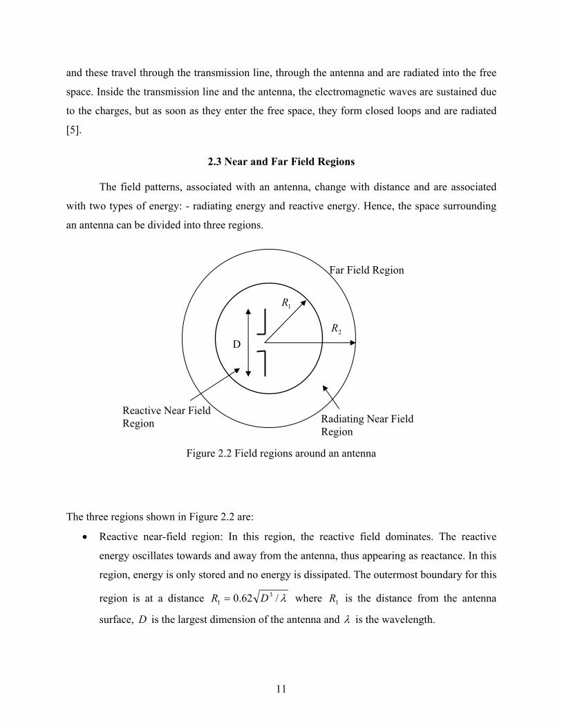
2.3 Near and Far Field Regions
The field patterns, associated with an antenna, change with distance and are associated
with two types of energy: - radiating energy and reactive energy. Hence, the space surrounding
an antenna can be divided into three regions.
Figure 2.2 Field regions around an antenna
The three regions shown in Figure 2.2 are:
• Reactive near-field region: In this region, the reactive field dominates. The reactive
energy oscillates towards and away from the antenna, thus appearing as reactance. In this
region, energy is only stored and no energy is dissipated. The outermost boundary for this
region is at a distance λ/62.0 31 DR = where 1R is the distance from the antenna
surface, D is the largest dimension of the antenna and λ is the wavelength.
D
1R
2R
Reactive Near Field Region Radiating Near Field
Region
Far Field Region
12
• Radiating near-field region (also called Fresnel region): This is the region which lies
between the reactive near-field region and the far field region. Reactive fields are smaller
in this field as compared to the reactive near-field region and the radiation fields
dominate. In this region, the angular field distribution is a function of the distance from
the antenna. The outermost boundary for this region is at a distance λ/2 22 DR = where
2R is the distance from the antenna surface.
• Far-field region (also called Fraunhofer region): The region beyond λ/2 22 DR = is the
far field region. In this region, the reactive fields are absent and only the radiation fields
exist. The angular field distribution is not dependent on the distance from the antenna in
this region and the power density varies as the inverse square of the radial distance in this
region.
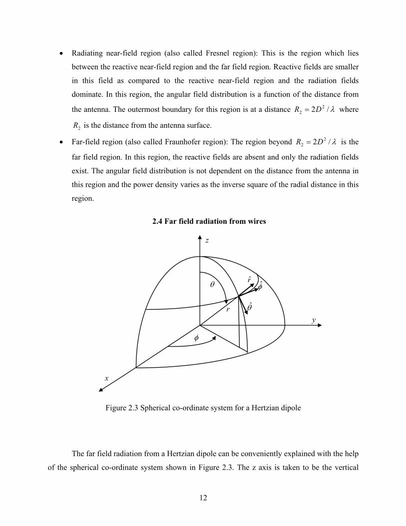
2.4 Far field radiation from wires
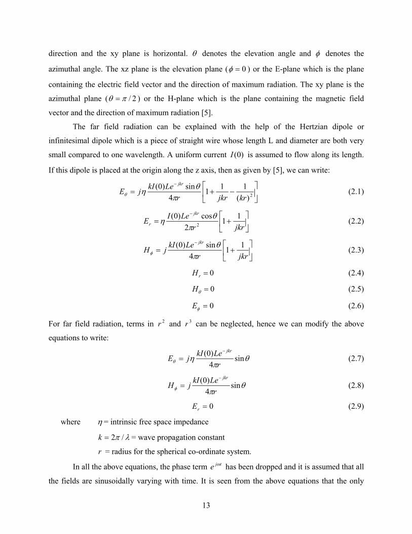
Figure 2.3 Spherical co-ordinate system for a Hertzian dipole
The far field radiation from a Hertzian dipole can be conveniently explained with the help
of the spherical co-ordinate system shown in Figure 2.3. The z axis is taken to be the vertical
θ
φ
x
y
z
r
rφ
θ
13
direction and the xy plane is horizontal. θ denotes the elevation angle and φ denotes the
azimuthal angle. The xz plane is the elevation plane ( 0=φ ) or the E-plane which is the plane
containing the electric field vector and the direction of maximum radiation. The xy plane is the
azimuthal plane ( 2/πθ = ) or the H-plane which is the plane containing the magnetic field
vector and the direction of maximum radiation [5].
The far field radiation can be explained with the help of the Hertzian dipole or
infinitesimal dipole which is a piece of straight wire whose length L and diameter are both very
small compared to one wavelength. A uniform current )0(I is assumed to flow along its length.
If this dipole is placed at the origin along the z axis, then as given by [5], we can write:
−+=
−
2)(111
4sin)0(
krjkrrLekIjE
jkr
πθηθ (2.1)
+=
−
jkrrLeIE
jkr
r11
2cos)0(
2πθη (2.2)
+=
−
jkrrLekIjH
jkr 114
sin)0(π
θφ (2.3)
0=rH (2.4)
0=θH (2.5)
0=φE (2.6)
For far field radiation, terms in 2r and 3r can be neglected, hence we can modify the above
equations to write:
θπ
ηθ sin4)0(rLekIjE
jkr−
= (2.7)
θπφ sin
4)0(rLekIjH
jkr−
= (2.8)
0=rE (2.9)
where η = intrinsic free space impedance
λπ /2=k = wave propagation constant
r = radius for the spherical co-ordinate system.
In all the above equations, the phase term tje ω has been dropped and it is assumed that all
the fields are sinusoidally varying with time. It is seen from the above equations that the only

14
non-zero fields are θE and φH , and that they are transverse to each other. The ratio θE / φH =η ,
such that the wave impedance is 120π and the fields are in phase and inversely proportional
to r . The directions of E , H and r form a right handed set such that the Poynting vector is in
the r direction and it indicates the direction of propagation of the electromagnetic wave. Hence
the time average poynting vector given by [5] can be written as:
]Re[21 *HEWav ×= )/( 2mWatts (2.10)
where E and H represent the peak values of the electric and magnetic fields respectively.
The average power radiated by an antenna can be written as:
∫∫= dsWP radrad (Watts ) (2.11)
where ds is the vector differential surface = rddr )φθθsin2
radW is the magnitude of the time average poynting vector )/( 2mWatts
The radiation intensity is defined as the power radiated from an antenna per unit solid angle and
is given as:
radWrU 2= (2.12)
where U is the radiation intensity in Watts per unit solid angle.
2.5 Antenna Performance Parameters
The performance of an antenna can be gauged from a number of parameters. Certain critical
parameters are discussed below.
2.5.1 Radiation Pattern
The radiation pattern of an antenna is a plot of the far-field radiation properties of an
antenna as a function of the spatial co-ordinates which are specified by the elevation angle θ and
the azimuth angleφ . More specifically it is a plot of the power radiated from an antenna per unit
solid angle which is nothing but the radiation intensity [5]. Let us consider the case of an
isotropic antenna. An isotropic antenna is one which radiates equally in all directions. If the total
power radiated by the isotropic antenna isP , then the power is spread over a sphere of radius r ,
so that the power density S at this distance in any direction is given as:

15
24 rP
areaPS
π== (2.13)
Then the radiation intensity for this isotropic antenna iU can be written as:
π42 PSrUi == (2.14)
An isotropic antenna is not possible to realize in practice and is useful only for
comparison purposes. A more practical type is the directional antenna which radiates more
power in some directions and less power in other directions. A special case of the directional
antenna is the omnidirectional antenna whose radiation pattern may be constant in one plane (e.g.
E-plane) and varies in an orthogonal plane (e.g. H-plane). The radiation pattern plot of a generic
directional antenna is shown in Figure 2.4.
Figure 2.4 Radiation pattern of a generic directional antenna
Figure 2.4 shows the following:
• HPBW: The half power beamwidth (HPBW) can be defined as the angle subtended
by the half power points of the main lobe.
• Main Lobe: This is the radiation lobe containing the direction of maximum radiation.
• Minor Lobe: All the lobes other then the main lobe are called the minor lobes. These
lobes represent the radiation in undesired directions. The level of minor lobes is
HPBW
Back Lobe
Side Lobe
Minor Lobes Main Lobe
Null

16
usually expressed as a ratio of the power density in the lobe in question to that of the
major lobe. This ratio is called as the side lobe level (expressed in decibels).
• Back Lobe: This is the minor lobe diametrically opposite the main lobe.
• Side Lobes: These are the minor lobes adjacent to the main lobe and are separated by
various nulls. Side lobes are generally the largest among the minor lobes.
In most wireless systems, minor lobes are undesired. Hence a good antenna design should
minimize the minor lobes.
2.5.2 Directivity
The directivity of an antenna has been defined by [5] as “the ratio of the radiation
intensity in a given direction from the antenna to the radiation intensity averaged over all
directions”. In other words, the directivity of a nonisotropic source is equal to the ratio of its
radiation intensity in a given direction, over that of an isotropic source.
PU
UUDi
π4== (2.15)
where D is the directivity of the antenna
U is the radiation intensity of the antenna
iU is the radiation intensity of an isotropic source
P is the total power radiated
Sometimes, the direction of the directivity is not specified. In this case, the direction of the
maximum radiation intensity is implied and the maximum directivity is given by [5] as:
PU
UU
Di
maxmaxmax
4π== (2.16)
where maxD is the maximum directivity
maxU is the maximum radiation intensity
Directivity is a dimensionless quantity, since it is the ratio of two radiation intensities.
Hence, it is generally expressed in dBi. The directivity of an antenna can be easily estimated
from the radiation pattern of the antenna. An antenna that has a narrow main lobe would have
better directivity, then the one which has a broad main lobe, hence it is more directive.

17
2.5.3 Input Impedance
The input impedance of an antenna is defined by [5] as “the impedance presented by an
antenna at its terminals or the ratio of the voltage to the current at the pair of terminals or the
ratio of the appropriate components of the electric to magnetic fields at a point”. Hence the
impedance of the antenna can be written as:
ininin jXRZ += (2.17)
where inZ is the antenna impedance at the terminals
inR is the antenna resistance at the terminals
inX is the antenna reactance at the terminals
The imaginary part, inX of the input impedance represents the power stored in the near
field of the antenna. The resistive part, inR of the input impedance consists of two components,
the radiation resistance rR and the loss resistance LR . The power associated with the radiation
resistance is the power actually radiated by the antenna, while the power dissipated in the loss
resistance is lost as heat in the antenna itself due to dielectric or conducting losses.
2.5.4 Voltage Standing Wave Ratio (VSWR)
Figure 2.5 Equivalent circuit of transmitting antenna
SZ
sR SX
rR
LR
inX
Transmitter Antenna
inZ
18
In order for the antenna to operate efficiently, maximum transfer of power must take
place between the transmitter and the antenna. Maximum power transfer can take place only
when the impedance of the antenna ( inZ ) is matched to that of the transmitter ( SZ ). According to
the maximum power transfer theorem, maximum power can be transferred only if the impedance
of the transmitter is a complex conjugate of the impedance of the antenna under consideration
and vice-versa. Thus, the condition for matching is:
inZ = *SZ (2.18)
where ininin jXRZ +=
SSS jXRZ += as shown in Figure 2.5
If the condition for matching is not satisfied, then some of the power maybe reflected
back and this leads to the creation of standing waves, which can be characterized by a parameter
called as the Voltage Standing Wave Ratio (VSWR).
The VSWR is given by Makarov [6] as:
Γ−
Γ+=
11
VSWR (2.19)
Sin
Sin
i
r
ZZZZ
VV
+−
==Γ (2.20)
where Γ is called the reflection coefficient
rV is the amplitude of the reflected wave
iV is the amplitude of the incident wave
The VSWR is basically a measure of the impedance mismatch between the transmitter
and the antenna. The higher the VSWR, the greater is the mismatch. The minimum VSWR
which corresponds to a perfect match is unity. A practical antenna design should have an input
impedance of either 50Ω or 75Ω since most radio equipment is built for this impedance.
2.5.5 Return Loss (RL)
The Return Loss (RL) is a parameter which indicates the amount of power that is “lost”
to the load and does not return as a reflection. As explained in the preceding section, waves are
reflected leading to the formation of standing waves, when the transmitter and antenna

19
impedance do not match. Hence the RL is a parameter similar to the VSWR to indicate how well
the matching between the transmitter and antenna has taken place. The RL is given as by [6] as:
Γ−= 10log20RL (dB) (2.21)
For perfect matching between the transmitter and the antenna, 0=Γ and ∞=RL which
means no power would be reflected back, whereas a 1=Γ has a 0=RL dB, which implies that
all incident power is reflected. For practical applications, a VSWR of 2 is acceptable, since this
corresponds to a RL of -9.54 dB.
2.5.6 Antenna Efficiency
The antenna efficiency is a parameter which takes into account the amount of losses at
the terminals of the antenna and within the structure of the antenna. These losses are given by [5]
as:
• Reflections because of mismatch between the transmitter and the antenna
• RI 2 losses (conduction and dielectric)
Hence the total antenna efficiency can be written as:
dcrt eeee = (2.22)
where te = total antenna efficiency
)1( 2Γ−=re = reflection (mismatch) efficiency
ce = conduction efficiency
de = dielectric efficiency
Since ce and de are difficult to separate, they are lumped together to form the cde efficiency
which is given as:
Lr
rdccd RR
Reee+
== (2.23)
cde is called as the antenna radiation efficiency and is defined as the ratio of the power delivered
to the radiation resistance rR , to the power delivered to rR and LR .

20
2.5.7 Antenna Gain
Antenna gain is a parameter which is closely related to the directivity of the antenna. We
know that the directivity is how much an antenna concentrates energy in one direction in
preference to radiation in other directions. Hence, if the antenna is 100% efficient, then the
directivity would be equal to the antenna gain and the antenna would be an isotropic radiator.
Since all antennas will radiate more in some direction that in others, therefore the gain is the
amount of power that can be achieved in one direction at the expense of the power lost in the
others as explained by Ulaby [7]. The gain is always related to the main lobe and is specified in
the direction of maximum radiation unless indicated. It is given as:
( ) ( )φθφθ ,, DeG cd= (dBi) (2.24)
2.5.8 Polarization
Polarization of a radiated wave is defined by [5] as “that property of an electromagnetic
wave describing the time varying direction and relative magnitude of the electric field vector”.
The polarization of an antenna refers to the polarization of the electric field vector of the radiated
wave. In other words, the position and direction of the electric field with reference to the earth’s
surface or ground determines the wave polarization. The most common types of polarization
include the linear (horizontal or vertical) and circular (right hand polarization or the left hand
polarization).
Figure 2.6 A linearly (vertically) polarized wave
xE
yH
z

21
If the path of the electric field vector is back and forth along a line, it is said to be linearly
polarized. Figure 2.6 shows a linearly polarized wave. In a circularly polarized wave, the electric
field vector remains constant in length but rotates around in a circular path. A left hand circular
polarized wave is one in which the wave rotates counterclockwise whereas right hand circular
polarized wave exhibits clockwise motion as shown in Figure 2.7.
Figure 2.7 Commonly used polarization schemes
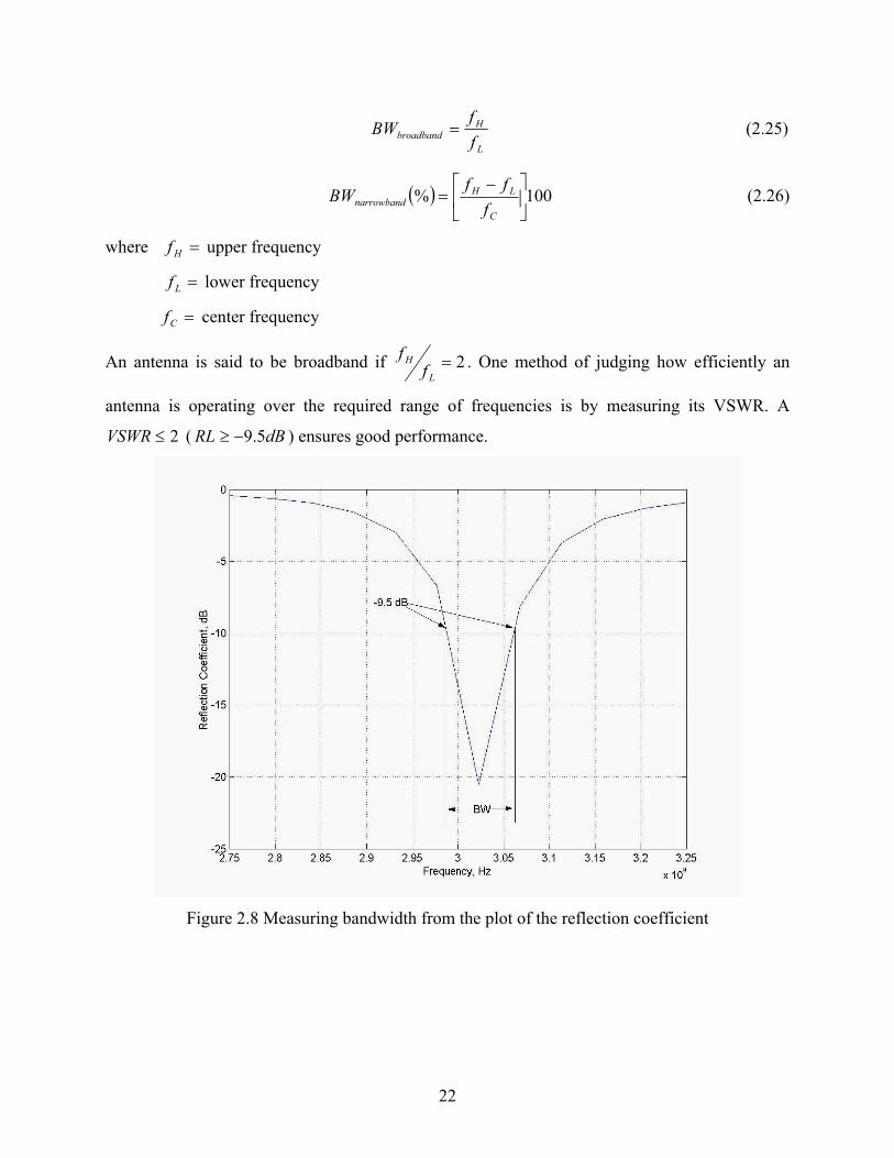
2.5.9 Bandwidth
The bandwidth of an antenna is defined by [5] as “the range of usable frequencies within
which the performance of the antenna, with respect to some characteristic, conforms to a
specified standard.” The bandwidth can be the range of frequencies on either side of the center
frequency where the antenna characteristics like input impedance, radiation pattern, beamwidth,
polarization, side lobe level or gain, are close to those values which have been obtained at the
center frequency. The bandwidth of a broadband antenna can be defined as the ratio of the upper
to lower frequencies of acceptable operation. The bandwidth of a narrowband antenna can be
defined as the percentage of the frequency difference over the center frequency [5]. According to
[4] these definitions can be written in terms of equations as follows:
E
Vertical Linear Polarization
E
Horizontal Linear Polarization
E
Right hand circular polarization
E
Left hand circular polarization
22
L
Hbroadband f
fBW = (2.25)
( ) 100%
−=
C
LHnarrowband f
ffBW (2.26)
where =Hf upper frequency
=Lf lower frequency
=Cf center frequency
An antenna is said to be broadband if 2=L
Hf
f . One method of judging how efficiently an
antenna is operating over the required range of frequencies is by measuring its VSWR. A
2≤VSWR ( dBRL 5.9−≥ ) ensures good performance.
Figure 2.8 Measuring bandwidth from the plot of the reflection coefficient

23
2.6 Types of Antennas
Antennas come in different shapes and sizes to suit different types of wireless
applications. The characteristics of an antenna are very much determined by its shape, size and
the type of material that it is made of. Some of the commonly used antennas are briefly described
below.
2.6.1 Half Wave Dipole
The length of this antenna is equal to half of its wavelength as the name itself suggests.
Dipoles can be shorter or longer than half the wavelength, but a tradeoff exists in the
performance and hence the half wavelength dipole is widely used.
Figure 2.9 Half wave dipole
The dipole antenna is fed by a two wire transmission line, where the two currents in the
conductors are of sinusoidal distribution and equal in amplitude, but opposite in direction.
Hence, due to canceling effects, no radiation occurs from the transmission line. As shown in
Figure 2.9, the currents in the arms of the dipole are in the same direction and they produce
radiation in the horizontal direction. Thus, for a vertical orientation, the dipole radiates in the
horizontal direction. The typical gain of the dipole is 2dB and it has a bandwidth of about 10%.
The half power beamwidth is about 78 degrees in the E plane and its directivity is 1.64 (2.15dB)
I
I
2λ
z
yx

24
with a radiation resistance of 73Ω [4]. Figure 2.10 shows the radiation pattern for the half wave
dipole.
Figure 2.10 Radiation pattern for Half wave dipole
2.6.2 Monopole Antenna The monopole antenna, shown in Figure 2.11, results from applying the image theory to
the dipole. According to this theory, if a conducting plane is placed below a single element of
length 2/L carrying a current, then the combination of the element and its image acts identically
to a dipole of length L except that the radiation occurs only in the space above the plane as
discussed by Saunders [8].
Figure 2.11 Monopole Antenna
z
y y
xElevation Azimuth
z
y
x
Ground plane 4λ
Monopole
Image
2λ

25
For this type of antenna, the directivity is doubled and the radiation resistance is halved
when compared to the dipole. Thus, a half wave dipole can be approximated by a quarter wave
monopole ( 4/2/ λ=L ). The monopole is very useful in mobile antennas where the conducting
plane can be the car body or the handset case. The typical gain for the quarter wavelength
monopole is 2-6dB and it has a bandwidth of about 10%. Its radiation resistance is 36.5Ω and its
directivity is 3.28 (5.16dB) [4]. The radiation pattern for the monopole is shown below in Figure
2.12.
Figure 2.12 Radiation pattern for the Monopole Antenna
2.6.3 Loop Antennas
The loop antenna is a conductor bent into the shape of a closed curve such as a circle or a
square with a gap in the conductor to form the terminals as shown in Figure 2.13. There are two
types of loop antennas-electrically small loop antennas and electrically large loop antennas. If the
total loop circumference is very small as compared to the wavelength ( λ<<<L ), then the loop
antenna is said to be electrically small. An electrically large loop antenna typically has its
circumference close to a wavelength. The far-field radiation patterns of the small loop antenna
are insensitive to shape [4].
z
y y
xElevation Azimuth

26
Figure 2.13 Loop Antenna As shown in Figure 2.14, the radiation patterns are identical to that of a dipole despite the
fact that the dipole is vertically polarized whereas the small circular loop is horizontally
polarized.
Figure 2.14 Radiation Pattern of Small and Large Loop Antenna
z
y
Elevation
y
xAzimuth
y
Azimuth x
z
y
Elevation
Small Loop Antenna
Large Loop Antenna
z
y
x
Small Circular Loop Antenna
z
y
x
4λ
Large Square Loop Antenna
27
The performance of the loop antenna can be increased by filling the core with ferrite.
This helps in increasing the radiation resistance. When the perimeter or circumference of the
loop antenna is close to a wavelength, then the antenna is said to be a large loop antenna.
The radiation pattern of the large loop antenna is different then that of the small loop
antenna. For a one wavelength square loop antenna, radiation is maximum normal to the plane of
the loop (along the z axis). In the plane of the loop, there is a null in the direction parallel to the
side containing the feed (along the x axis), and there is a lobe in a direction perpendicular to the
side containing the feed (along the y axis). Loop antennas generally have a gain from -2dB to
3dB and a bandwidth of around 10%. . The small loop antenna is very popular as a receiving
antenna [4]. Single turn loop antennas are used in pagers and multiturn loop antennas are used in
AM broadcast receivers.
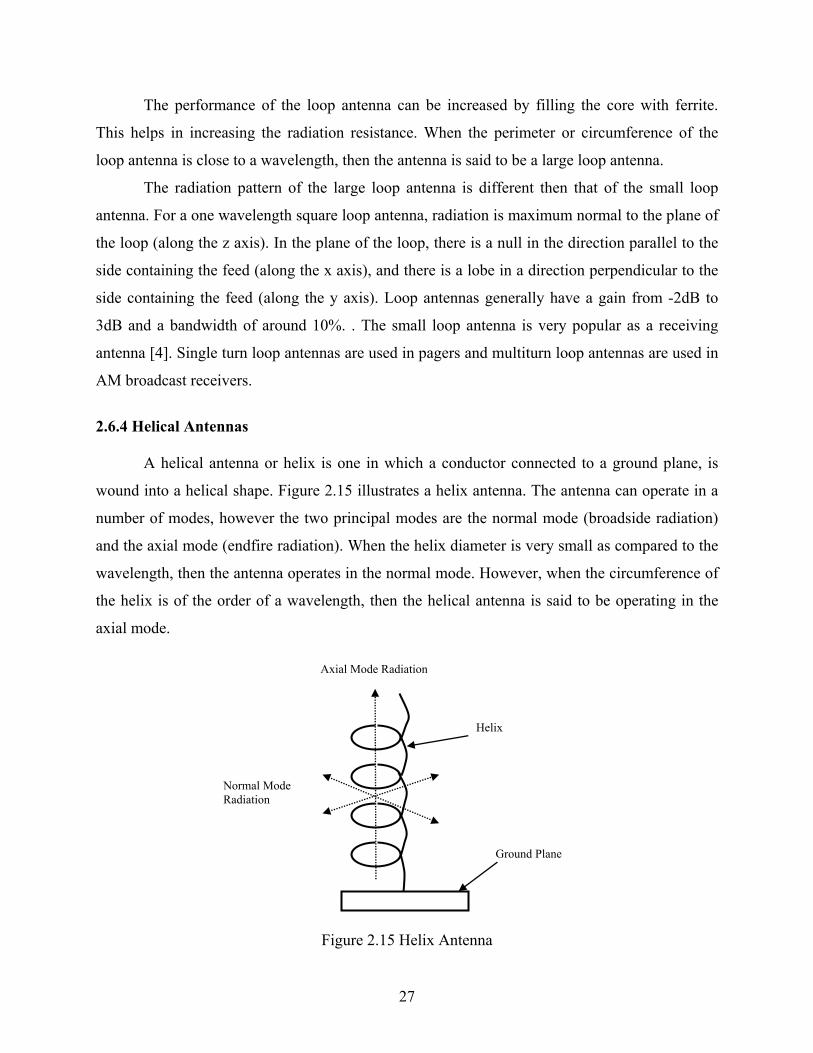
2.6.4 Helical Antennas
A helical antenna or helix is one in which a conductor connected to a ground plane, is
wound into a helical shape. Figure 2.15 illustrates a helix antenna. The antenna can operate in a
number of modes, however the two principal modes are the normal mode (broadside radiation)
and the axial mode (endfire radiation). When the helix diameter is very small as compared to the
wavelength, then the antenna operates in the normal mode. However, when the circumference of
the helix is of the order of a wavelength, then the helical antenna is said to be operating in the
axial mode.
Figure 2.15 Helix Antenna
Helix
Ground Plane
Normal Mode Radiation
Axial Mode Radiation

28
In the normal mode of operation, the antenna field is maximum in a plane normal to the
helix axis and minimum along its axis. This mode provides low bandwidth and is generally used
for hand-portable mobile applications [8].
Figure 2.16 Radiation Pattern of Helix Antenna
In the axial mode of operation, the antenna radiates as an endfire radiator with a single
beam along the helix axis. This mode provides better gain (upto 15dB) [4] and high bandwidth
ratio (1.78:1) as compared to the normal mode of operation. For this mode of operation, the
beam becomes narrower as the number of turns on the helix is increased. Due to its broadband
nature of operation, the antenna in the axial mode is used mainly for satellite communications.
Figure 2.16 above shows the radiation patterns for the normal mode as well as the axial mode of
operations.
z
y
Elevation
y
xAzimuth
z
Normal Mode Axial Mode

29
2.6.5 Horn Antennas
Horn antennas are used typically in the microwave region (gigahertz range) where
waveguides are the standard feed method, since horn antennas essentially consist of a waveguide
whose end walls are flared outwards to form a megaphone like structure.
Figure 2.17 Types of Horn Antenna
Horns provide high gain, low VSWR, relatively wide bandwidth, low weight, and are
easy to construct [4]. The aperture of the horn can be rectangular, circular or elliptical. However,
rectangular horns are widely used. The three basic types of horn antennas that utilize a
rectangular geometry are shown in Figure 2.17. These horns are fed by a rectangular waveguide
which have a broad horizontal wall as shown in the figure. For dominant waveguide mode
excitation, the E-plane is vertical and H-plane horizontal. If the broad wall dimension of the horn
is flared with the narrow wall of the waveguide being left as it is, then it is called an H-plane
sectoral horn antenna as shown in the figure. If the flaring occurs only in the E-plane dimension,
it is called an E-plane sectoral horn antenna. A pyramidal horn antenna is obtained when flaring
occurs along both the dimensions. The horn basically acts as a transition from the waveguide
mode to the free-space mode and this transition reduces the reflected waves and emphasizes the
traveling waves which lead to low VSWR and wide bandwidth [4]. The horn is widely used as a
feed element for large radio astronomy, satellite tracking, and communication dishes.
E E
E
E-plane Horn Antenna H-plane Horn Antenna
Pyramidal Horn Antenna

30
In the above sections, several antennas have been discussed. Another commonly used
antenna is the Microstrip patch antenna. The aim of this thesis is to design a compact microstrip
patch antenna to be used in wireless communication and this antenna is explained in the next
chapter.
31
CHAPTER 3
MICROSTRIP PATCH ANTENNA
In this chapter, an introduction to the Microstrip Patch Antenna is followed by its
advantages and disadvantages. Next, some feed modeling techniques are discussed. Finally, a
detailed explanation of Microstrip patch antenna analysis and its theory are discussed, and also
the working mechanism is explained.
3.1 Introduction
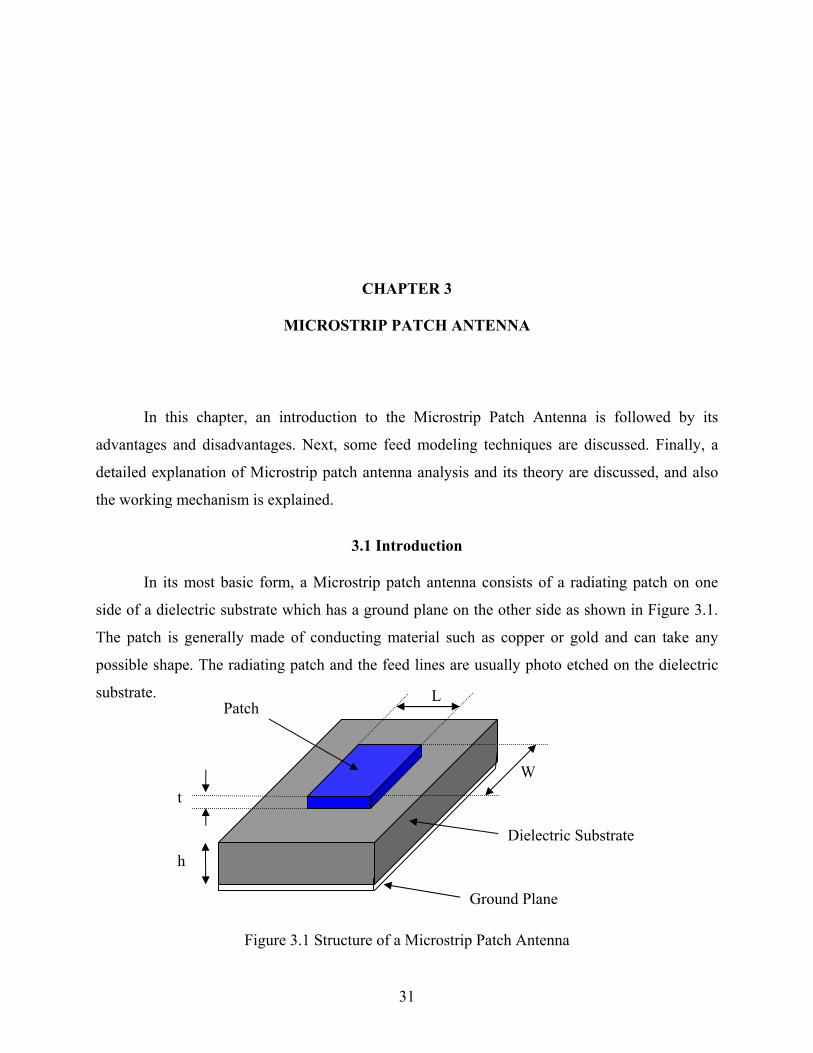
In its most basic form, a Microstrip patch antenna consists of a radiating patch on one
side of a dielectric substrate which has a ground plane on the other side as shown in Figure 3.1.
The patch is generally made of conducting material such as copper or gold and can take any
possible shape. The radiating patch and the feed lines are usually photo etched on the dielectric
substrate.
Figure 3.1 Structure of a Microstrip Patch Antenna
Ground Plane
Patch
Dielectric Substrate
t
h
W
L

32
In order to simplify analysis and performance prediction, the patch is generally square,
rectangular, circular, triangular, elliptical or some other common shape as shown in Figure 3.2.
For a rectangular patch, the length L of the patch is usually oo L λλ 5.03333.0 << , where oλ is
the free-space wavelength. The patch is selected to be very thin such that ot λ<< (where t is the
patch thickness). The height h of the dielectric substrate is usually 0.003 oo h λλ 05.0≤≤ . The
dielectric constant of the substrate ( rε ) is typically in the range 122.2 ≤≤ rε .
Figure 3.2 Common shapes of microstrip patch elements
Microstrip patch antennas radiate primarily because of the fringing fields between the
patch edge and the ground plane. For good antenna performance, a thick dielectric substrate
having a low dielectric constant is desirable since this provides better efficiency, larger
bandwidth and better radiation [5]. However, such a configuration leads to a larger antenna size.
In order to design a compact Microstrip patch antenna, higher dielectric constants must be used
which are less efficient and result in narrower bandwidth. Hence a compromise must be reached
between antenna dimensions and antenna performance.
3.2 Advantages and Disadvantages
Microstrip patch antennas are increasing in popularity for use in wireless applications due
to their low-profile structure. Therefore they are extremely compatible for embedded antennas in
handheld wireless devices such as cellular phones, pagers etc... The telemetry and
Square Rectangular Dipole Circular
EllipticalTriangular Circular Ring

33
communication antennas on missiles need to be thin and conformal and are often Microstrip
patch antennas. Another area where they have been used successfully is in Satellite
communication. Some of their principal advantages discussed by [5] and Kumar and Ray [9] are
given below:
• Light weight and low volume.
• Low profile planar configuration which can be easily made conformal to host surface.
• Low fabrication cost, hence can be manufactured in large quantities.
• Supports both, linear as well as circular polarization.
• Can be easily integrated with microwave integrated circuits (MICs).
• Capable of dual and triple frequency operations.
• Mechanically robust when mounted on rigid surfaces.
Microstrip patch antennas suffer from a number of disadvantages as compared to
conventional antennas. Some of their major disadvantages discussed by [9] and Garg et al [10]
are given below:
• Narrow bandwidth
• Low efficiency
• Low Gain
• Extraneous radiation from feeds and junctions
• Poor end fire radiator except tapered slot antennas
• Low power handling capacity.
• Surface wave excitation
Microstrip patch antennas have a very high antenna quality factor (Q). Q represents the
losses associated with the antenna and a large Q leads to narrow bandwidth and low efficiency.
Q can be reduced by increasing the thickness of the dielectric substrate. But as the thickness
increases, an increasing fraction of the total power delivered by the source goes into a surface
wave. This surface wave contribution can be counted as an unwanted power loss since it is
ultimately scattered at the dielectric bends and causes degradation of the antenna characteristics.
However, surface waves can be minimized by use of photonic bandgap structures as discussed
by Qian et al [11]. Other problems such as lower gain and lower power handling capacity can be
overcome by using an array configuration for the elements.

34
3.3 Feed Techniques
Microstrip patch antennas can be fed by a variety of methods. These methods can be
classified into two categories- contacting and non-contacting. In the contacting method, the RF
power is fed directly to the radiating patch using a connecting element such as a microstrip line.
In the non-contacting scheme, electromagnetic field coupling is done to transfer power between
the microstrip line and the radiating patch [5]. The four most popular feed techniques used are
the microstrip line, coaxial probe (both contacting schemes), aperture coupling and proximity
coupling (both non-contacting schemes).
3.3.1 Microstrip Line Feed
In this type of feed technique, a conducting strip is connected directly to the edge of the
microstrip patch as shown in Figure 3.3. The conducting strip is smaller in width as compared to
the patch and this kind of feed arrangement has the advantage that the feed can be etched on the
same substrate to provide a planar structure.
Figure 3.3 Microstrip Line Feed
The purpose of the inset cut in the patch is to match the impedance of the feed line to the
patch without the need for any additional matching element. This is achieved by properly
controlling the inset position. Hence this is an easy feeding scheme, since it provides ease of
Substrate
Ground Plane
Microstrip Feed Patch

35
fabrication and simplicity in modeling as well as impedance matching. However as the thickness
of the dielectric substrate being used, increases, surface waves and spurious feed radiation also
increases, which hampers the bandwidth of the antenna [5]. The feed radiation also leads to
undesired cross polarized radiation.
3.3.2 Coaxial Feed
The Coaxial feed or probe feed is a very common technique used for feeding Microstrip
patch antennas. As seen from Figure 3.4, the inner conductor of the coaxial connector extends
through the dielectric and is soldered to the radiating patch, while the outer conductor is
connected to the ground plane.
Figure 3.4 Probe fed Rectangular Microstrip Patch Antenna The main advantage of this type of feeding scheme is that the feed can be placed at any
desired location inside the patch in order to match with its input impedance. This feed method is
easy to fabricate and has low spurious radiation. However, its major disadvantage is that it
Ground PlaneCoaxial Connector
Substrate
Patch

36
provides narrow bandwidth and is difficult to model since a hole has to be drilled in the substrate
and the connector protrudes outside the ground plane, thus not making it completely planar for
thick substrates ( oh λ02.0> ). Also, for thicker substrates, the increased probe length makes the
input impedance more inductive, leading to matching problems [9]. It is seen above that for a
thick dielectric substrate, which provides broad bandwidth, the microstrip line feed and the
coaxial feed suffer from numerous disadvantages. The non-contacting feed techniques which
have been discussed below, solve these problems.
3.3.3 Aperture Coupled Feed
In this type of feed technique, the radiating patch and the microstrip feed line are
separated by the ground plane as shown in Figure 3.5. Coupling between the patch and the feed
line is made through a slot or an aperture in the ground plane.
Figure 3.5 Aperture-coupled feed The coupling aperture is usually centered under the patch, leading to lower cross-
polarization due to symmetry of the configuration. The amount of coupling from the feed line to
the patch is determined by the shape, size and location of the aperture. Since the ground plane
separates the patch and the feed line, spurious radiation is minimized. Generally, a high dielectric
Ground Plane Substrate 2
Substrate 1
Microstrip Line Patch Aperture/Slot

37
material is used for the bottom substrate and a thick, low dielectric constant material is used for
the top substrate to optimize radiation from the patch [5]. The major disadvantage of this feed
technique is that it is difficult to fabricate due to multiple layers, which also increases the
antenna thickness. This feeding scheme also provides narrow bandwidth.
3.3.4 Proximity Coupled Feed
This type of feed technique is also called as the electromagnetic coupling scheme. As
shown in Figure 3.6, two dielectric substrates are used such that the feed line is between the two
substrates and the radiating patch is on top of the upper substrate. The main advantage of this
feed technique is that it eliminates spurious feed radiation and provides very high bandwidth (as
high as 13%) [5], due to overall increase in the thickness of the microstrip patch antenna. This
scheme also provides choices between two different dielectric media, one for the patch and one
for the feed line to optimize the individual performances.
Figure 3.6 Proximity-coupled Feed
Matching can be achieved by controlling the length of the feed line and the width-to-line
ratio of the patch. The major disadvantage of this feed scheme is that it is difficult to fabricate
Microstrip Line
Patch
Substrate 1
Substrate 2

38
because of the two dielectric layers which need proper alignment. Also, there is an increase in
the overall thickness of the antenna.
Table 3.1 below summarizes the characteristics of the different feed techniques.
Table 3.1 Comparing the different feed techniques [4] Characteristics Microstrip Line
Feed
Coaxial Feed Aperture
coupled Feed
Proximity
coupled Feed
Spurious feed radiation
More More Less Minimum
Reliability Better Poor due to
soldering
Good Good
Ease of fabrication
Easy Soldering and
drilling needed
Alignment
required
Alignment
required
Impedance Matching
Easy Easy Easy Easy
Bandwidth (achieved with impedance matching)
2-5% 2-5% 2-5% 13%
3.4 Methods of Analysis
The most popular models for the analysis of Microstrip patch antennas are the
transmission line model, cavity model, and full wave model [5] (which include primarily integral
equations/Moment Method). The transmission line model is the simplest of all and it gives good
physical insight but it is less accurate. The cavity model is more accurate and gives good
physical insight but is complex in nature. The full wave models are extremely accurate, versatile
and can treat single elements, finite and infinite arrays, stacked elements, arbitrary shaped
elements and coupling. These give less insight as compared to the two models mentioned above
and are far more complex in nature.
39
3.4.1 Transmission Line Model
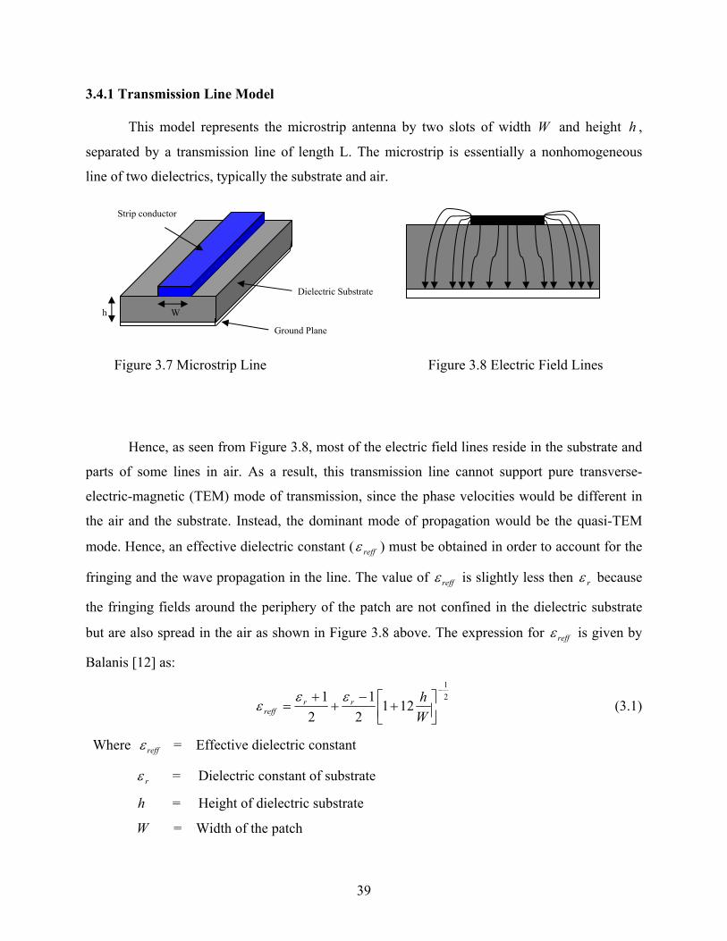
This model represents the microstrip antenna by two slots of width W and height h ,
separated by a transmission line of length L. The microstrip is essentially a nonhomogeneous
line of two dielectrics, typically the substrate and air.
Figure 3.7 Microstrip Line Figure 3.8 Electric Field Lines Hence, as seen from Figure 3.8, most of the electric field lines reside in the substrate and
parts of some lines in air. As a result, this transmission line cannot support pure transverse-
electric-magnetic (TEM) mode of transmission, since the phase velocities would be different in
the air and the substrate. Instead, the dominant mode of propagation would be the quasi-TEM
mode. Hence, an effective dielectric constant ( reffε ) must be obtained in order to account for the
fringing and the wave propagation in the line. The value of reffε is slightly less then rε because
the fringing fields around the periphery of the patch are not confined in the dielectric substrate
but are also spread in the air as shown in Figure 3.8 above. The expression for reffε is given by
Balanis [12] as:
21
1212
12
1 −
+
−+
+=
Whrr
reffεε
ε (3.1)
Where reffε = Effective dielectric constant
rε = Dielectric constant of substrate
h = Height of dielectric substrate
W = Width of the patch
Ground Plane
Dielectric Substrate
h W
Strip conductor

40
Consider Figure 3.9 below, which shows a rectangular microstrip patch antenna of
length L , width W resting on a substrate of heighth . The co-ordinate axis is selected such that
the length is along the x direction, width is along the y direction and the height is along the z
direction.
Figure 3.9 Microstrip Patch Antenna
In order to operate in the fundamental 10TM mode, the length of the patch must be
slightly less than 2/λ where λ is the wavelength in the dielectric medium and is equal to
reffo ελ / where oλ is the free space wavelength. The 10TM mode implies that the field varies
one 2/λ cycle along the length, and there is no variation along the width of the patch. In the
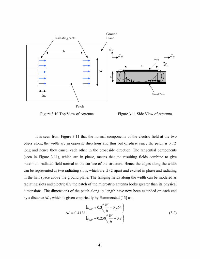
Figure 3.10 shown below, the microstrip patch antenna is represented by two slots, separated by
a transmission line of length L and open circuited at both the ends. Along the width of the patch,
the voltage is maximum and current is minimum due to the open ends. The fields at the edges
can be resolved into normal and tangential components with respect to the ground plane.
h Substrate
Ground Plane
Microstrip Feed Patch
W
L
x
y z
41
Figure 3.10 Top View of Antenna Figure 3.11 Side View of Antenna
It is seen from Figure 3.11 that the normal components of the electric field at the two
edges along the width are in opposite directions and thus out of phase since the patch is 2/λ
long and hence they cancel each other in the broadside direction. The tangential components
(seen in Figure 3.11), which are in phase, means that the resulting fields combine to give
maximum radiated field normal to the surface of the structure. Hence the edges along the width
can be represented as two radiating slots, which are 2/λ apart and excited in phase and radiating
in the half space above the ground plane. The fringing fields along the width can be modeled as
radiating slots and electrically the patch of the microstrip antenna looks greater than its physical
dimensions. The dimensions of the patch along its length have now been extended on each end
by a distance L∆ , which is given empirically by Hammerstad [13] as:
( )
( )
+−
++
=∆8.0258.0
264.03.0412.0
hWhW
hLreff
reff
ε
ε (3.2)
L
W
Radiating Slots
Patch
Ground Plane
L∆
h
Patch
Ground Plane
L
VE
HE HE
VE

42
The effective length of the patch effL now becomes:
LLLeff ∆+= 2 (3.3)
For a given resonance frequency of , the effective length is given by [9] as:
reffo
eff fcLε2
= (3.4)
For a rectangular Microstrip patch antenna, the resonance frequency for any mnTM mode is
given by James and Hall [14] as:
21
22
2
+
=
Wn
Lmcf
reffo ε
(3.5)
Where m and n are modes along L and W respectively.
For efficient radiation, the width W is given by Bahl and Bhartia [15] as:
( )
212 +
=r
of
cWε
(3.6)
3.4.2 Cavity Model
Although the transmission line model discussed in the previous section is easy to use, it
has some inherent disadvantages. Specifically, it is useful for patches of rectangular design and it
ignores field variations along the radiating edges. These disadvantages can be overcome by using
the cavity model. A brief overview of this model is given below.
In this model, the interior region of the dielectric substrate is modeled as a cavity
bounded by electric walls on the top and bottom. The basis for this assumption is the following
observations for thin substrates ( )λ<<h [10].
• Since the substrate is thin, the fields in the interior region do not vary much in the z
direction, i.e. normal to the patch.
• The electric field is z directed only, and the magnetic field has only the transverse
components xH and yH in the region bounded by the patch metallization and the ground
plane. This observation provides for the electric walls at the top and the bottom.

43
Figure 3.12 Charge distribution and current density creation on the microstrip patch
Consider Figure 3.12 shown above. When the microstrip patch is provided power, a
charge distribution is seen on the upper and lower surfaces of the patch and at the bottom of the
ground plane. This charge distribution is controlled by two mechanisms-an attractive mechanism
and a repulsive mechanism as discussed by Richards [16]. The attractive mechanism is between
the opposite charges on the bottom side of the patch and the ground plane, which helps in
keeping the charge concentration intact at the bottom of the patch. The repulsive mechanism is
between the like charges on the bottom surface of the patch, which causes pushing of some
charges from the bottom, to the top of the patch. As a result of this charge movement, currents
flow at the top and bottom surface of the patch. The cavity model assumes that the height to
width ratio (i.e. height of substrate and width of the patch) is very small and as a result of this the
attractive mechanism dominates and causes most of the charge concentration and the current to
be below the patch surface. Much less current would flow on the top surface of the patch and as
the height to width ratio further decreases, the current on the top surface of the patch would be
almost equal to zero, which would not allow the creation of any tangential magnetic field
components to the patch edges. Hence, the four sidewalls could be modeled as perfectly
magnetic conducting surfaces. This implies that the magnetic fields and the electric field
distribution beneath the patch would not be disturbed. However, in practice, a finite width to
height ratio would be there and this would not make the tangential magnetic fields to be
completely zero, but they being very small, the side walls could be approximated to be perfectly
magnetic conducting [5].
- - -
- - ---
+ + +
+ + ++ +
W
h
tJ
bJ+ + + + + + - - - - - - - - -

44
Since the walls of the cavity, as well as the material within it are lossless, the cavity
would not radiate and its input impedance would be purely reactive. Hence, in order to account
for radiation and a loss mechanism, one must introduce a radiation resistance rR and a loss
resistance LR . A lossy cavity would now represent an antenna and the loss is taken into account
by the effective loss tangent effδ which is given as:
Teff Q/1=δ (3.7)
TQ is the total antenna quality factor and has been expressed by [4] in the form:
rcdT QQQQ
1111++= (3.8)
• dQ represents the quality factor of the dielectric and is given as :
δ
ωtan
1==
d
Trd P
WQ (3.9)
where rω is the angular resonant frequency.
TW is the total energy stored in the patch at resonance.
dP is the dielectric loss.
δtan is the loss tangent of the dielectric.
• cQ represents the quality factor of the conductor and is given as :
∆
==h
PW
Qc
Trc
ω (3.10)
where cP is the conductor loss.
∆ is the skin depth of the conductor.
h is the height of the substrate.
• rQ represents the quality factor for radiation and is given as:
r
Trr P
WQ
ω= (3.11)
where rP is the power radiated from the patch.
Substituting equations (3.8), (3.9), (3.10) and (3.11) in equation (3.7), we get
Tr
reff W
Ph ω
δδ +∆
+= tan (3.12)

45
Thus, equation (3.12) describes the total effective loss tangent for the microstrip patch antenna.
3.4.3 Full Wave Solutions-Method of Moments
One of the methods, that provide the full wave analysis for the microstrip patch antenna,
is the Method of Moments. In this method, the surface currents are used to model the microstrip
patch and the volume polarization currents are used to model the fields in the dielectric slab. It
has been shown by Newman and Tulyathan [17] how an integral equation is obtained for these
unknown currents and using the Method of Moments, these electric field integral equations are
converted into matrix equations which can then be solved by various techniques of algebra to
provide the result. A brief overview of the Moment Method described by Harrington [18] and [5]
is given below.
The basic form of the equation to be solved by the Method of Moment is:
hgF =)( (3.13)
where F is a known linear operator, g is an unknown function, and h is the source or
excitation function. The aim here is to find g , when F and h are known. The unknown function
g can be expanded as a linear combination of N terms to give:
∑=
+++==N
nNNnn gagagagag
12211 ....... (3.14)
where na is an unknown constant and ng is a known function usually called a basis or
expansion function. Substituting equation (3.14) in (3.13) and using the linearity property of the
operatorF , we can write:
∑=
=N
nnn hgFa
1)( (3.15)
The basis functions ng must be selected in such a way, that each )( ngF in the above
equation can be calculated. The unknown constants na cannot be determined directly because
there are N unknowns, but only one equation. One method of finding these constants is the
method of weighted residuals. In this method, a set of trial solutions is established with one or
more variable parameters. The residuals are a measure of the difference between the trial
solution and the true solution. The variable parameters are selected in a way which guarantees a
best fit of the trial functions based on the minimization of the residuals. This is done by defining

46
a set of N weighting (or testing) functions Nm wwww ,....., 21= in the domain of the
operatorF . Taking the inner product of these functions, equation (3.15) becomes:
∑=
⟩⟨=⟩⟨N
nmnmn hwgFwa
1,)(, (3.16)
where Nm ,.....2,1=
Writing in Matrix form as shown in [5], we get:
[ ][ ] [ ]mnmn haF = (3.17)
where
[ ]
⟩⟩⟨⟨⟩⟩⟨⟨
=
M
M
.........)(,)(,.........)(,)(,
2212
2111
gFwgFwgFwgFw
Fmn [ ]
=
N
n
a
aaa
aM
3
2
1
[ ]
⟩⟨
⟩⟨⟩⟨⟩⟨
=
hw
hwhwhw
h
N
m
,
,,,
3
2
1
M
The unknown constants na can now be found using algebraic techniques such as LU
decomposition or Gaussian elimination. It must be remembered that the weighting functions
must be selected appropriately so that elements of nw are not only linearly independent but
they also minimize the computations required to evaluate the inner product. One such choice of
the weighting functions may be to let the weighting and the basis function be the same, that is,
.nn gw = This is called as the Galerkin’s Method as described by Kantorovich and Akilov [19].
From the antenna theory point of view, we can write the Electric field integral equation as:
)(JfE e= (3.18)
where E is the known incident electric field.
J is the unknown induced current.
ef is the linear operator.
The first step in the moment method solution process would be to expand J as a finite sum of
basis function given as:
∑=
=M
iiibJJ
1 (3.19)

47
where ib is the ith basis function and iJ is an unknown coefficient. The second step involves the
defining of a set of M linearly independent weighting functions, jw . Taking the inner product on
both sides and substituting equation (3.19) in equation (3.18) we get:
∑=
⟩⟨=⟩⟨M
iiiejj bJfwEw
1
),(,, (3.20)
where Mj ,.....2,1=
Writing in Matrix form as,
[ ][ ] [ ]jij EJZ = (3.21)
where ⟩⟨= )(, iejij bfwZ
⟩⟨= HwE jj ,
J is the current vector containing the unknown quantities.
The vector E contains the known incident field quantities and the terms of the Z matrix
are functions of geometry. The unknown coefficients of the induced current are the terms of the
J vector. Using any of the algebraic schemes mentioned earlier, these equations can be solved to
give the current and then the other parameters such as the scattered electric and magnetic fields
can be calculated directly from the induced currents. Thus, the Moment Method has been briefly
explained for use in antenna problems. The software used in this thesis, Zeland Inc’s IE3D [20]
is a Moment Method simulator. Further details about the software will be provided in the next
chapter.

48
CHAPTER 4
MICROSTRIP PATCH ANTENNA DESIGN AND RESULTS
In this chapter, the procedure for designing a rectangular microstrip patch antenna is
explained. Next, a compact rectangular microstrip patch antenna is designed for use in cellular
phones. Finally, the results obtained from the simulations are demonstrated.
4.1 Design Specifications
The three essential parameters for the design of a rectangular Microstrip Patch Antenna
are:
• Frequency of operation ( of ): The resonant frequency of the antenna must be selected
appropriately. The Personal Communication System (PCS) uses the frequency range
from 1850-1990 MHz. Hence the antenna designed must be able to operate in this
frequency range. The resonant frequency selected for my design is 1.9 GHz.
• Dielectric constant of the substrate ( rε ): The dielectric material selected for my design is
Silicon which has a dielectric constant of 11.9. A substrate with a high dielectric constant
has been selected since it reduces the dimensions of the antenna.
• Height of dielectric substrate (h ): For the microstrip patch antenna to be used in cellular
phones, it is essential that the antenna is not bulky. Hence, the height of the dielectric
substrate is selected as 1.5 mm.

49
Hence, the essential parameters for the design are:
• of = 1.9 GHz
• rε = 11.9
• h = 1.5 mm
4.2 Design Procedure
Figure 4.1 Top view of Microstrip Patch Antenna
The transmission line model described in chapter 3 will be used to design the antenna.
Step 1: Calculation of the Width (W ): The width of the Microstrip patch antenna is given by
equation (3.6) as:
( )2
12 +=
rof
cWε
(4.1)
gL
L
W
),( ff YX
gW
Feed Point
Patch
Ground Plane

50
Substituting c = 3e8 m/s, rε = 11.9 and of = 1.9 GHz, we get:
W = 0.0311 m = 31.1 mm
Step 2: Calculation of Effective dielectric constant ( reffε ): Equation (3.1) gives the effective
dielectric constant as:
21
1212
12
1 −
+
−+
+=
Whrr
reffεε
ε (4.2)
Substituting rε = 11.9, W = 31.1 mm and h = 1.5 mm we get:
reffε = 10.7871
Step 3: Calculation of the Effective length ( effL ): Equation (3.4) gives the effective length as:
reffoeff f
cLε2
= (4.3)
Substituting reffε = 10.7871, c = 3e8 m/s and of = 1.9 GHz we get:
effL = 0.024 m = 24 mm
Step 4: Calculation of the length extension ( L∆ ): Equation (3.2) gives the length extension
as:
( )
( )
+−
++
=∆8.0258.0
264.03.0412.0
hWhW
hLreff
reff
ε
ε (4.4)
Substituting reffε = 10.7871, W = 31.1 mm and h = 1.5 mm we get:

51
L∆ = 6.3455 e-4 mm
Step 5: Calculation of actual length of patch ( L ): The actual length is obtained by re-writing
equation (3.3) as:
LLL eff ∆−= 2 (4.5)
Substituting effL = 24 mm and L∆ = 6.3455 e-4 mm we get:
L = 0.0228 m = 22.8 mm
Step 6: Calculation of the ground plane dimensions ( gL and gW ):
The transmission line model is applicable to infinite ground planes only. However, for
practical considerations, it is essential to have a finite ground plane. It has been shown by [9] that
similar results for finite and infinite ground plane can be obtained if the size of the ground plane
is greater than the patch dimensions by approximately six times the substrate thickness all around
the periphery. Hence, for this design, the ground plane dimensions would be given as:
mmLhLg 8.318.22)5.1(66 =+=+=
mmWhWg 1.401.31)5.1(66 =+=+=
Step 7: Determination of feed point location ( ff YX , ):
A coaxial probe type feed is to be used in this design. As shown in Figure 4.1, the center
of the patch is taken as the origin and the feed point location is given by the co-ordinates
( ff YX , ) from the origin. The feed point must be located at that point on the patch, where the
input impedance is 50 ohms for the resonant frequency. Hence, a trial and error method is used
to locate the feed point. For different locations of the feed point, the return loss (R.L) is
compared and that feed point is selected where the R.L is most negative. According to [5] there
exists a point along the length of the patch where the R.L is minimum. Hence in this design, fY
will be zero and only fX will be varied to locate the optimum feed point.
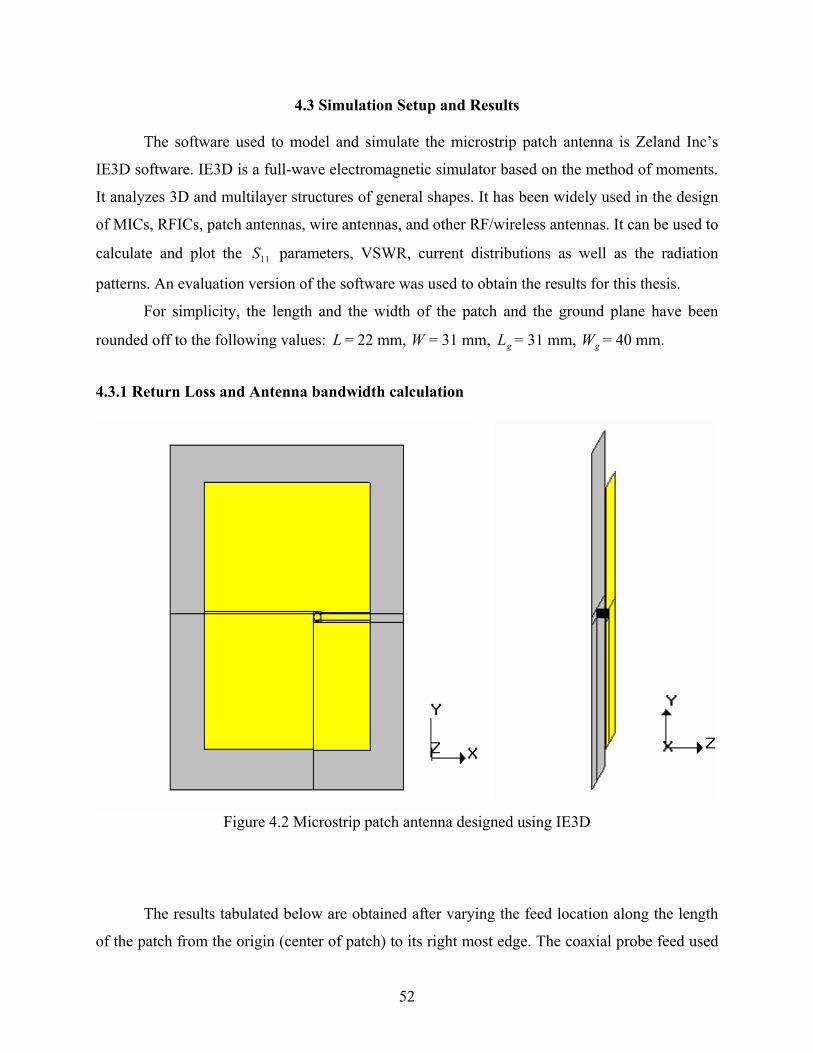
52
4.3 Simulation Setup and Results
The software used to model and simulate the microstrip patch antenna is Zeland Inc’s
IE3D software. IE3D is a full-wave electromagnetic simulator based on the method of moments.
It analyzes 3D and multilayer structures of general shapes. It has been widely used in the design
of MICs, RFICs, patch antennas, wire antennas, and other RF/wireless antennas. It can be used to
calculate and plot the 11S parameters, VSWR, current distributions as well as the radiation
patterns. An evaluation version of the software was used to obtain the results for this thesis.
For simplicity, the length and the width of the patch and the ground plane have been
rounded off to the following values: L = 22 mm, W = 31 mm, gL = 31 mm, gW = 40 mm.
4.3.1 Return Loss and Antenna bandwidth calculation
Figure 4.2 Microstrip patch antenna designed using IE3D
The results tabulated below are obtained after varying the feed location along the length
of the patch from the origin (center of patch) to its right most edge. The coaxial probe feed used

53
is designed to have a radius of 0.5mm. A frequency range of 1.7-2.1 GHz is selected and 401
frequency points are selected over this range to obtain accurate results. Table 4.1 shows the
calculated results for different feed locations.
Table 4.1 Effect of feed location on center frequency, return loss and bandwidth
No.
Feed Location
( ff YX , )
(mm)
Center Frequency
(GHz)
Return Loss (RL)
(dB)
Bandwidth
(RL > -9.5dB)
(MHz)
1 (1,0) 1.9153 -1.1384 -
2 (2,0) 1.9147 -4.5967 -
3 (3,0) 1.9127 -10.9602 9.97
4 (3.25,0) 1.9133 -13.3696 15.32
5 (3.5,0) 1.9127 -16.6242 18.84
6 (3.75,0) 1.9127 -21.2769 21.43
7 (4,0) 1.9120 -31.3585 23.28
8 (4.25,0) 1.9127 -28.5068 24.40
9 (4.5,0) 1.9127 -21.2952 25.16
10 (4.75,0) 1.9120 -17.6845 25.23
11 (5,0) 1.9120 -15.0623 24.30
12 (6,0) 1.9087 -10.2221 13.57
13 (7,0) 1.9087 -7.7754 -
14 (8,0) 1.9087 -6.3367 -
15 (9,0) 1.9073 -5.5806 -
16 (10,0) 1.9073 -5.0228 -

54
Figure 4.3 below shows the return loss plots for some of the feed point locations.
Figure 4.3 Return loss for feed located at different locations
The center frequency is selected as the one at which the return loss is minimum. As
described in chapter 2, the bandwidth can be calculated from the return loss (RL) plot. The
bandwidth of the antenna can be said to be those range of frequencies over which the RL is
greater than -9.5 dB (-9.5 dB corresponds to a VSWR of 2 which is an acceptable figure). From
table 4.1, the optimum feed point is found to be at ( ff YX , ) = (4, 0) where a RL of -31.3585 dB
is obtained. The bandwidth of the antenna for this feed point location is calculated (as shown
below in Figure 4.4) to be 23.28 MHz and a center frequency of 1.9120 GHz is obtained which is
very close to the desired design frequency of 1.9 GHz. It is observed from the table that, as the
feed point location is moved away from the center of the patch, the center frequency starts to

55
decrease slightly. It is also seen that though the maximum return loss is obtained at ( ff YX , ) =
(4, 0), the maximum bandwidth is obtained at ( ff YX , ) = (4.75, 0).
Figure 4.4 Return loss for feed located at (4, 0)
4.3.2 Radiation Pattern plots
Since a microstrip patch antenna radiates normal to its patch surface, the elevation pattern
for φ = 0 and φ = 90 degrees would be important. Figure 4.5 below shows the gain of the
antenna at 1.9120 GHz for φ = 0 and φ = 90 degrees.
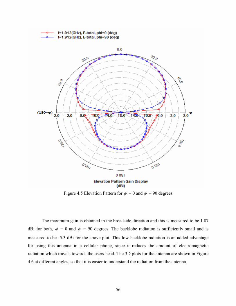
56
Figure 4.5 Elevation Pattern for φ = 0 and φ = 90 degrees
The maximum gain is obtained in the broadside direction and this is measured to be 1.87
dBi for both, φ = 0 and φ = 90 degrees. The backlobe radiation is sufficiently small and is
measured to be -5.3 dBi for the above plot. This low backlobe radiation is an added advantage
for using this antenna in a cellular phone, since it reduces the amount of electromagnetic
radiation which travels towards the users head. The 3D plots for the antenna are shown in Figure
4.6 at different angles, so that it is easier to understand the radiation from the antenna.
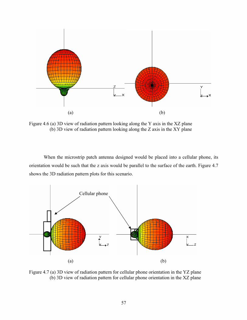
57
(a) (b) Figure 4.6 (a) 3D view of radiation pattern looking along the Y axis in the XZ plane (b) 3D view of radiation pattern looking along the Z axis in the XY plane When the microstrip patch antenna designed would be placed into a cellular phone, its
orientation would be such that the z axis would be parallel to the surface of the earth. Figure 4.7
shows the 3D radiation pattern plots for this scenario.
(a) (b) Figure 4.7 (a) 3D view of radiation pattern for cellular phone orientation in the YZ plane (b) 3D view of radiation pattern for cellular phone orientation in the XZ plane
Cellular phone

58
4.3.3 Other calculated parameters Some of the other calculated parameters, such as the gain, directivity, antenna efficiency
and 3 dB beamwidth for the antenna at 1.912 GHz are given below.
• Gain = 1.8717 dBi
• Directivity = 5.56 dBi
• Antenna Efficiency = 42.77%
• 3 dB Beamwidth = (106.85, 110.24) degrees

59
CHAPTER 5
CONCLUSIONS
The aim of this thesis was to design a compact microstrip patch antenna for use in
wireless/cellular devices. A typical cellular phone measures about 14.5 cm by 4.5 cm. Hence the
antenna designed must be able to fit in such a cellular phone. As demonstrated by the design and
the results obtained in chapter 4, a compact microstrip patch antenna has been successfully
designed having a center frequency of 1.91 GHz. The ground plane dimensions for the patch
antenna have been designed to be 31 mm by 40 mm and the patch dimensions are 22 mm by 31
mm. Hence the designed antenna is compact enough to be placed in a typical cellular phone.
Radiation pattern plots have been obtained for the desired antenna orientation. Reduced back
lobe radiation was obtained which is an added advantage for the application of the antenna in
cellular handsets since this minimizes the amount of electromagnetic energy radiated towards the
users head. A gain of 1.87 dBi and directivity of 5.56 dBi were obtained. The bandwidth
obtained for this antenna is 23.28 MHz which should be sufficient for cellular devices in the PCS
range since TDMA and GSM systems use 30 KHz channels.
Another area for future work is to extend this concept to a multiband design. It is
envisioned in the future, that a single handset would serve a number of applications. When the
user would be at home, the handset would operate in the same frequency range as used by
cordless phones and thus would be connected to the local telephone exchange. When the user
would be outside his house, the handset would connect to the cellular network. On a business trip
away from home, the handset would then connect though the satellite network to provide service
to the user. These different networks would require that the antenna in the handset is able to

60
operate at separate frequencies. The antenna designed in this thesis is a uniband antenna centered
at 1.91 GHz. Work must be done to design a dichroic or trichroic microstrip parch antenna which
can operate at two or three frequencies to serve multiple applications.