
The fabrication and characterisation of metal oxide thin films for
176
The fabrication and characterisation of metal oxide thin films for microelectronic and optical applications Matthew R. Field B.App.Sci (App.Phys)(Hons) A thesis written for the fulfilment of the requirements for the degree Doctor of Philosophy School of Applied Sciences College of Science, Engineering and Health RMIT University Melbourne, Australia May, 2011
Transcript of The fabrication and characterisation of metal oxide thin films for
The fabrication and characterisation of
metal oxide thin films for
microelectronic and optical applications
Matthew R. Field
B.App.Sci (App.Phys)(Hons)
A thesis written for the fulfilment of the requirements
for the degree Doctor of Philosophy
School of Applied Sciences
College of Science, Engineering and Health
RMIT University
Melbourne, Australia
May, 2011


I
“It’s a long walk back to Eden, sweetheart, so don’t sweat the small stuff!”
-Carolyn Roberts, “Insomnia” by Stephen King
"Be faithful in small things because it is in them that your strength lies."
-Mother Teresa

II
Declaration
I certify that except where due acknowledgement has been made, the work is that of the author
alone; the work has not been submitted previously, in whole or in part, to qualify for any other
academic award; the content of the thesis is the result of work which has been carried out since
the official commencement date of the approved research program; any editorial work, paid or
unpaid, carried out by a third party is acknowledged; and, ethics procedures and guidelines
have been followed.
.........................................
Matthew Field
31 May 2011

III
Acknowledgements
First of all I would like to thank the people who helped me throughout this long endeavour in
completing my PhD and writing this thesis. To my supervisor Prof. Dougal McCulloch who has
not only guided me but has also taught me many valuable things in work and in life. Granted,
on some occasions I might have come to your views kicking and screaming, but the experience
was definitely valuable.
I would also like to thank my other supervisor, even if he fervently denies being it, Dr. James
Partridge. Without your influence, I would possibly never have looked into gate dielectrics or
gas sensors, and I would certainly be left sitting in the labs scratching my head over E(J)
curves! I would also like to thank the many people that I have worked with over the years, Dr.
Andre Anders, Dr Sunnie Lim and Dr. Jeff Brown for instilling a fascination of electrochromic
materials and solar cells into me. It was an absolute pleasure working with you people and I
hope to see you all again in Berkeley labs sometime in the near future.
I‟d like to next thank the contributions of the RMMF and RMIT staff. Without Phil Francis and
Peter Rummel, the RMIT microscopy suite would surely fall into chaos. I would also like to
thank Ju Lin Peng, who has helped me in making TEM samples. Next I have many thanks for
my co-workers, Dr Desmond Lau, Dr Nemo Biluš Abaffy, Arwen Pagon, Ali Moafi and Ben
Kent for keeping me sane while in the lab, and the rest of the RMIT staff for keeping
lunchtimes entertaining with the superquiz and fun chatter. Many thanks also go to my dear
friends Tasha, Jarrad and Aaron, whom I would never have gotten through my undergraduate
degree without! Whether you believe it or not, all of you were all very important to me during
my undergrad.

IV
Finally, to all the people out there outside of physics who have supported me through this long
and frustrating time. I am REALLY sorry that I keep talking thin film coatings at you and
making you zone out! Don‟t get me wrong, I do see your eyes glaze over from time to time, but
sometimes I can‟t help myself and need to get it fully out of my system! So a big thankyou to
my housemates Mark, Clifty, Zack, Ria and Rowan for keeping my life in check outside of
work.
The last of the people for me to thank are my brother Nathan and my Mum. Without you guys,
I‟m not sure where I would be right now let-alone being up at 3am writing thesis chapters. But
for what it‟s all worth, I am happy with where I am and who I am. And for that, I‟m always
grateful.
~Matt
V
Authors Publications
[1] Field MR, Partridge JG, Du Plessis J, McCulloch DG. Hafnium oxide thin films
deposited from a filtered cathodic vacuum arc. Applied Physics A: Materials Science
& Processing. 2009;97(3):627-33.
[2] Field MR, McCulloch DG, Lim SNH, Anders A, Keast VJ, Burgess RW. The electronic
structure of tungsten oxide thin films prepared by pulsed cathodic arc deposition and
plasma-assisted pulsed magnetron sputtering. Journal of Physics: Condensed Matter.
2008;20(17):175216.
[3] Partridge JG, Field MR, Peng JL, Sadek AZ, Kalantar-zadeh K, Plessis JD, et al.
Nanostructured SnO2 films prepared from evaporated Sn and their application as
gas sensors. Nanotechnology. 2008;19(12):125504.
[4] Partridge JG, Field MR, Sadek AZ, Kalantar-zadeh K, Du Plessis J, Taylor MB, et al.
Fabrication, Structural Characterization and Testing of a Nanostructured Tin Oxide Gas
Sensor. Sensors Journal, IEEE. 2009;9(5):563-8.
[5] Field MR, Partridge JG, Mayes EH, Latham K, McCulloch DG. The relationship
between microstructure and electrical breakdown in cathodic arc deposited hafnium
oxide films. Journal of Applied Physics. Submitted for publication 2010.
VI
Conference Presentations
[1] The synthesis and characterisation of tungsten oxide thin films
ACMM Conference, 11th -15th February 2008 (Perth, Australia)
M. R. Field, D. G. McCulloch, S.N.H. Lim, A. Anders, V. J. Keast, R. W. Burgess
[2] Analysis of metal oxide thin films deposited using a filtered cathodic vacuum arc
ACMM Conference, 11th-15th February 2008 (Perth, Australia)
J. G. Partridge, M. Field, N. Biluš Abaffy, J. Du Plessis and D. G. McCulloch
[3] Deposition of high quality metal oxide thin films using an FCVA
Poster at 15th AINSE Conference on Nuclear and Complementary Techniques of
Analysis (NCTA), 21st – 23rd November 2007 (Melbourne, Australia)
N. Biluš Abaffy, M. Field, J. G. Partridge, J. Du Plessis and D. G. McCulloch
[4] A study of the morphology and stoichiometry of nanostructured SnO2 thin films
Poster at ICONN 08, January 2008 (Melbourne, Australia).
J. G. Partridge, M. Field, J. Du Plessis, J. Yu and D. G. McCulloch
[5] Improving aluminum doped zinc oxide films by minimizing negative ion damage
ICCG 8 - International Conference on Coatings on Glass and Plastics
June 13 - 17, 2010, (Braunschweig, Germany)
André Anders, Jeff Brown, Sunnie Lim, Rueben Mendelsberg, Leonardo Gontijo, Kin
Man Yu, and Matthew Field
[6] Microstructural analysis of zinc oxide films doped with aluminium for solar cell
research
21st Australian Conference on Microscopy & Microanalysis
July 11 - 15, 2010, (Brisbane, Australia)
Matthew Field, André Anders, Jeff Brown and Dougal McCulloch
VII
Abstract
Metal oxide thin films are the subject of considerable research due to their novel optical and
electrical properties which make them suitable for use in many applications. These applications
include gas sensors, solar cell arrays, anti dazzling rear view mirrors, smart windows, display
devices, gate dielectrics, semiconductors and many more. The possibilities for new metal oxide
based materials is forever growing with the introduction of novel deposition methods which
allow precise control of the deposition parameters and the ability to dope in order to tailor
properties. The conditions used for the deposition of these coatings has an influence on the
microstructure which in turn plays an important role in determining physical properties, such as
the optical transmission and electrical conductivity. In addition, for many metal oxide materials
the structure-property relationship is not well understood. The aim of this thesis was two-fold.
Firstly, to deposit some metal oxide thin film coatings using several physical vapour deposition
techniques and characterise their microstructure and physical properties. Secondly, to make a
comparison between films deposited using different techniques to determine how the properties
of a film depend on the conditions under which they are formed.
To achieve these aims, tungsten oxide, zinc oxide doped with aluminium (also known as
aluminium zinc oxide - AZO) and hafnium oxide coatings were deposited and the
microstructure and physical properties were investigated. For tungsten oxide deposition, films
were deposited using pulsed magnetron sputtering and pulsed cathodic arc. It was found that
films deposited using magnetron sputtering were highly disordered. In contrast, those deposited
with cathodic arc were a highly ordered and exhibited a tetragonal phase, usually only observed
at high temperatures.
In the case of AZO, films were deposited using pulsed cathodic arc, pulsed magnetron
sputtering and high power impulse magnetron sputtering (HIPIMS). The pulsed cathodic arc
VIII
films were found to have both good transmittance in the visible region and the best resistivity of
all of the samples.
It was found that magnetron and HIPIMS produced films that exhibited non-uniform properties
across their surface due to in situ oxygen bombardment during deposition. This undesirable
effect was eliminated by incorporating a novel magnetic filter into the deposition setup which
acted to improve both the crystallinity and the resistivity. This thesis also performed the first
comprehensive investigation of hafnium oxide films prepared using a filtered cathodic vacuum
arc. Samples deposited at high substrate biases were found to damage readily which made
them electrically leaky. Samples deposited at room temperature were found to have a
disordered microstructure and had a good electrical breakdown. At elevated temperatures the
crystallinity of the samples increased, resulting in a microstructure containing large monoclinic
crystals. However, it was also found that the electrical breakdown worsened at elevated
temperatures, in agreement with other researchers who also find that hafnium oxide films with
disordered microstructure have the best electrical characteristics.
Ab initio calculations of the near edge structure found in x-ray and electron loss edges were
found to be a powerful way of distinguishing between the phases of tungsten oxide.
IX
Table of Contents
DECLARATION ....................................................................................................................... II
ACKNOWLEDGEMENTS .................................................................................................... III
AUTHORS PUBLICATIONS .................................................................................................. V
CONFERENCE PRESENTATIONS ..................................................................................... VI
ABSTRACT ............................................................................................................................ VII
TABLE OF CONTENTS ........................................................................................................ IX
LIST OF FIGURES .............................................................................................................. XIII
LIST OF TABLES .................................................................................................................. XX
CHAPTER 1 ................................................................................................................................ 1
INTRODUCTION ...................................................................................................................... 1
1.1 BIBLIOGRAPHY ............................................................................................................................. 7
CHAPTER 2 .............................................................................................................................. 10
BACKGROUND ....................................................................................................................... 10
2.1 METAL OXIDE DEPOSITION ..................................................................................................... 11
2.1.1 Cathodic arc deposition ............................................................................................ 11
2.1.2 Filtered cathodic vacuum arc (FCVA) deposition..................................................... 12
2.1.3 Pulsed cathodic arc deposition.................................................................................. 15
2.1.4 Magnetron sputtering ................................................................................................ 16
2.1.5 High power impulse magnetron sputtering (HIPIMS) .............................................. 17
2.2 EXPERIMENTAL ANALYSIS METHODS ................................................................................. 19
2.2.1 Scanning electron microscopy (SEM) ....................................................................... 19
2.2.2 Atomic force microscopy (AFM) ............................................................................... 19
2.2.2 X-ray diffraction (XRD) ............................................................................................. 19
2.2.3 X-ray photoelectron spectroscopy (XPS) .................................................................. 20
2.2.4 Optical transmission .................................................................................................. 21
2.2.5 Resistivity and Hall measurements ............................................................................ 22
2.2.6 Breakdown voltage .................................................................................................... 23
2.2.7 Transmission electron microscopy (TEM) sample preparation ................................ 23
2.2.8 TEM and selected area electron diffraction (SAED) ................................................. 25
2.2.9 Electron energy loss spectroscopy (EELS) ................................................................ 26
2.2.10 Energy loss near edge structure (ELNES) ............................................................... 28
X
2.2.11 X-ray absorption near edge structure (XANES) ...................................................... 28
2.3 THEORETICAL METHODS ......................................................................................................... 31
2.3.1 Multiple scattering calculations using the FEFF code .............................................. 31
2.3.2 Band structure calculations using the WIEN2k code ................................................ 34
2.4 BIBLIOGRAPHY ........................................................................................................................... 35
CHAPTER 3 .............................................................................................................................. 37
THE MICROSTRUCTURE AND ELECTRONIC STRUCTURE OF TUNGSTEN
OXIDE THIN FILMS ............................................................................................................... 37
3.1 INTRODUCTION .......................................................................................................................... 38
3.1.2 The crystal structure of WO3 ..................................................................................... 38
3.1.3 Growth of thin films of WO3 ...................................................................................... 41
3.2 EXPERIMENTAL TECHNIQUES ................................................................................................ 44
3.2.1 Deposition using pulsed cathodic arc ........................................................................ 44
3.2.2 Deposition using magnetron sputtering ..................................................................... 44
3.2.2 Theoretical methods ................................................................................................... 45
3.3 RESULTS AND DISCUSSIONS ................................................................................................... 46
3.3.1 X-ray photoelectron spectroscopy (XPS) ................................................................... 46
3.3.2 Cross sectional transmission electron microscopy (TEM) ........................................ 47
3.3.4 Electron energy loss spectroscopy (EELS) ................................................................ 51
3.3.4 Local density of states (LDOS) .................................................................................. 52
3.3.5 Energy-loss near edge structure (ELNES) ................................................................. 52
3.4 CONCLUSIONS ............................................................................................................................. 58
3.5 BIBLIOGRAPHY ........................................................................................................................... 59
CHAPTER 4 .............................................................................................................................. 62
MICROSTRUCTURAL ANALYSIS OF ZINC OXIDE FILMS DOPED WITH
ALUMINIUM FOR SOLAR CELL RESEARCH................................................................. 62
4.1 INTRODUCTION/BACKGROUND THEORY ............................................................................ 63
4.1.1 Doped zinc oxide in industry ..................................................................................... 63
4.1.2 Crystal structure and doping ..................................................................................... 63
4.1.3 AZO coatings ............................................................................................................. 65
4.1.4 Presence of negative ions in magnetron sputtering techniques ................................. 68
4.2. EXPERIMENTAL METHODS ..................................................................................................... 69
4.2.1 Pulsed cathodic arc ................................................................................................... 69
4.2.2 Magnetron sputtering ................................................................................................ 71
4.2.3 High power impulse magnetron sputtering (HIPIMS) ............................................... 71
4.2.4 Negative ion filter in magnetron deposition .............................................................. 71
XI
4.3. PULSED CATHODIC ARC DEPOSITED FILMS ...................................................................... 73
4.3.1 Resistivity and Hall Effect ......................................................................................... 73
4.3.2 Optical transmission .................................................................................................. 74
4.3.3 Composition and microstructure ............................................................................... 75
4.4 MAGNETRON SPUTTERED FILMS ........................................................................................... 83
4.4.1 Resistivity and Hall Effect ......................................................................................... 83
4.4.2 Optical transmission .................................................................................................. 84
4.4.3 Composition and microstructure ............................................................................... 85
4.5 HIPIMS ........................................................................................................................................... 91
4.5.1 Resistivity and Hall Effect ......................................................................................... 91
4.5.2 Optical transmission .................................................................................................. 93
4.5.3 Composition and microstructure ............................................................................... 94
4.6 FILTERED HIPIMS ..................................................................................................................... 101
4.6.1 Resistivity and Hall Effect ....................................................................................... 101
4.6.2 Optical transmission ................................................................................................ 101
4.6.3 Composition and microstructure ............................................................................. 102
4.7 COMPARISON OF TECHNIQUES ............................................................................................ 108
4.7 CONCLUSIONS .......................................................................................................................... 111
4.8 BIBLIOGRAPHY ......................................................................................................................... 113
CHAPTER 5 ............................................................................................................................ 116
THE MICROSTRUCTURE AND ELECTRICAL PROPERTIES................................... 116
OF HAFNIUM OXIDE PREPARED USING FILTERED CATHODIC VACUUM ARC
.................................................................................................................................................. 116
5.1 INTRODUCTION ........................................................................................................................ 117
5.1.1 Hafnium oxide as a dielectric .................................................................................. 117
5.1.2 Crystal structure of HfO2 ......................................................................................... 118
5.1.3 Hafnium oxide films ................................................................................................. 120
5.2 EXPERIMENTAL TECHNIQUES .............................................................................................. 121
5.3 THE EFFECT OF SUBSTRATE BIAS ON HAFNIUM OXIDE FILMS SYNTHESISED USING
FCVA .................................................................................................................................................. 122
5.3.1 X-ray photoelectron spectroscopy (XPS) ................................................................ 123
5.3.2 Film topography ...................................................................................................... 124
5.3.3 Transmission electron microscopy (TEM) .............................................................. 127
5.3.4 Electron energy loss spectroscopy (EELS) .............................................................. 130
5.3.5 Electrical breakdown ............................................................................................... 131

XII
5.4 THE EFFECT OF SUBSTRATE TEMPERATURE ON HAFNIUM OXIDE FILMS
SYNTHESISED USING FCVA ......................................................................................................... 132
5.4.1 X-ray photoelectron spectroscopy (XPS) ................................................................. 132
5.4.2 X-ray diffraction (XRD) ........................................................................................... 135
5.4.3 Transmission electron microscopy (TEM) ............................................................... 137
5.4.4 X-ray absorption spectroscopy (XAS) ...................................................................... 140
5.4.5 Electrical breakdown ............................................................................................... 142
5.6 CONCLUSIONS ........................................................................................................................... 144
5.7 BIBLIOGRAPHY ......................................................................................................................... 144
CHAPTER 6 ............................................................................................................................ 148
CONCLUSIONS AND FUTURE WORK ............................................................................ 148
XIII
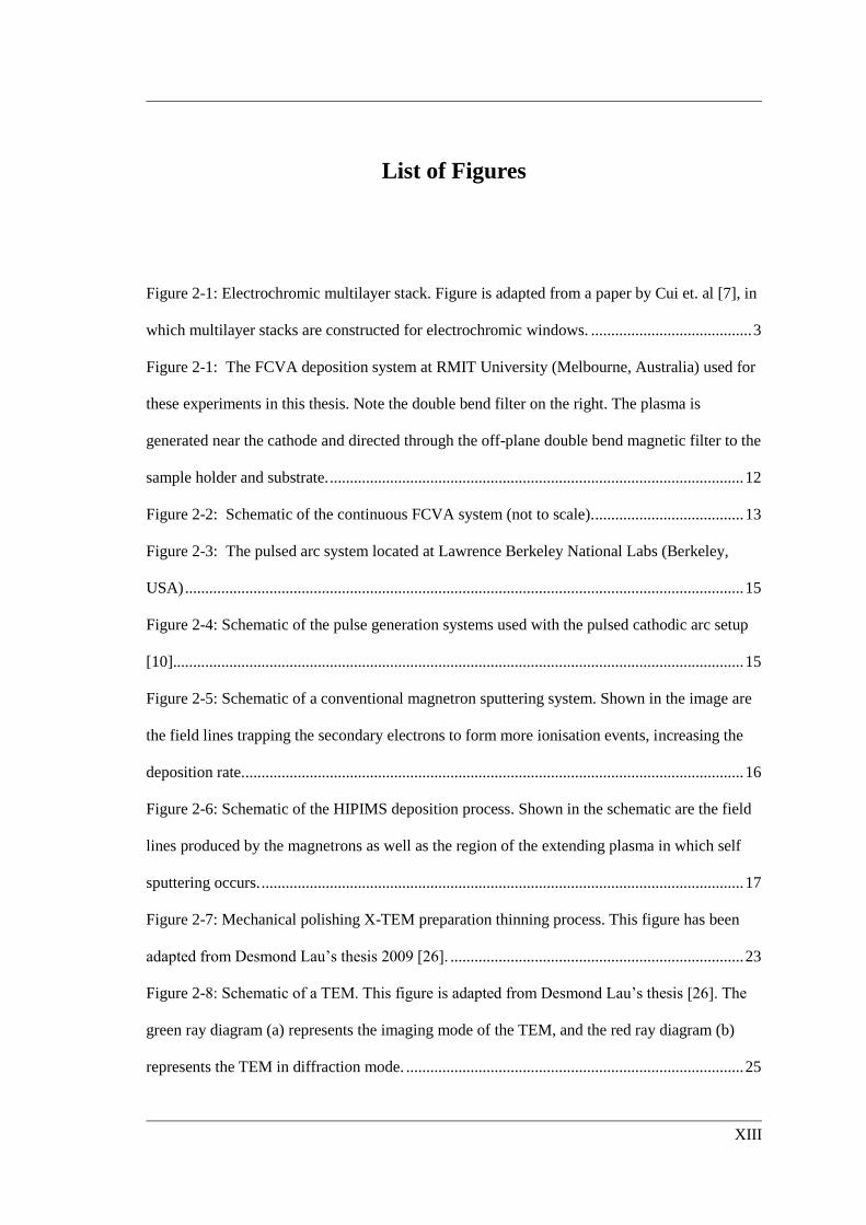
List of Figures
Figure 2-1: Electrochromic multilayer stack. Figure is adapted from a paper by Cui et. al [7], in
which multilayer stacks are constructed for electrochromic windows. ........................................ 3
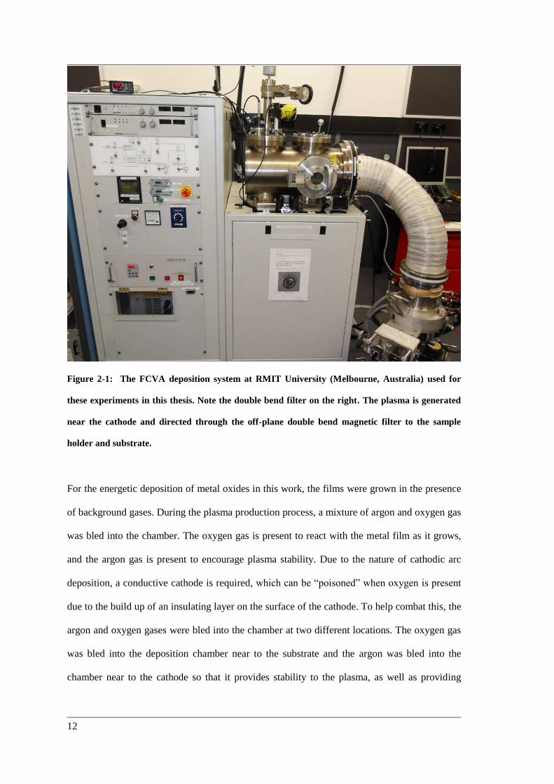
Figure 2-1: The FCVA deposition system at RMIT University (Melbourne, Australia) used for
these experiments in this thesis. Note the double bend filter on the right. The plasma is
generated near the cathode and directed through the off-plane double bend magnetic filter to the
sample holder and substrate. ....................................................................................................... 12
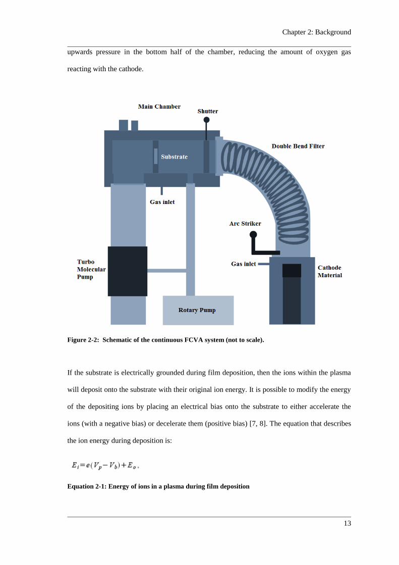
Figure 2-2: Schematic of the continuous FCVA system (not to scale). ..................................... 13
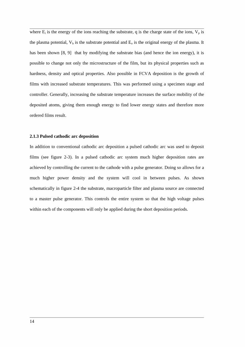
Figure 2-3: The pulsed arc system located at Lawrence Berkeley National Labs (Berkeley,
USA) ........................................................................................................................................... 15
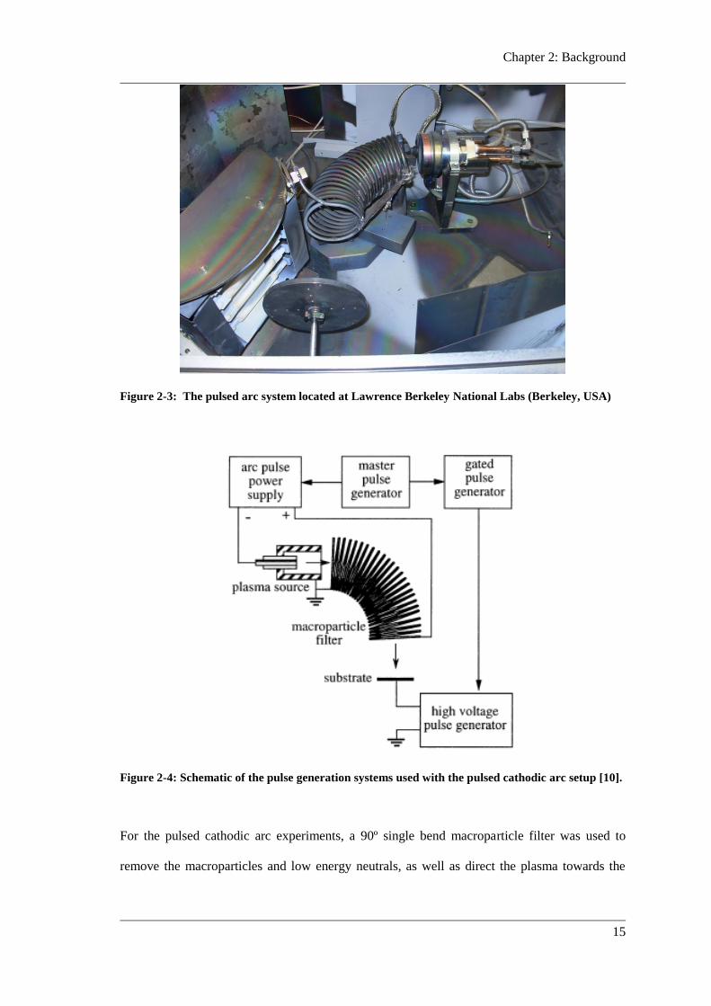
Figure 2-4: Schematic of the pulse generation systems used with the pulsed cathodic arc setup
[10].............................................................................................................................................. 15
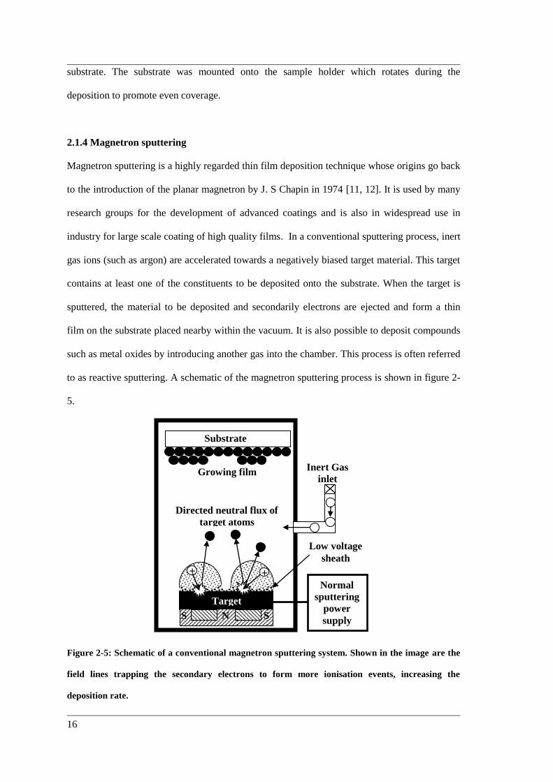
Figure 2-5: Schematic of a conventional magnetron sputtering system. Shown in the image are
the field lines trapping the secondary electrons to form more ionisation events, increasing the
deposition rate. ............................................................................................................................ 16
Figure 2-6: Schematic of the HIPIMS deposition process. Shown in the schematic are the field
lines produced by the magnetrons as well as the region of the extending plasma in which self
sputtering occurs. ........................................................................................................................ 17
Figure 2-7: Mechanical polishing X-TEM preparation thinning process. This figure has been
adapted from Desmond Lau‟s thesis 2009 [26]. ......................................................................... 23
Figure 2-8: Schematic of a TEM. This figure is adapted from Desmond Lau‟s thesis [26]. The
green ray diagram (a) represents the imaging mode of the TEM, and the red ray diagram (b)
represents the TEM in diffraction mode. .................................................................................... 25
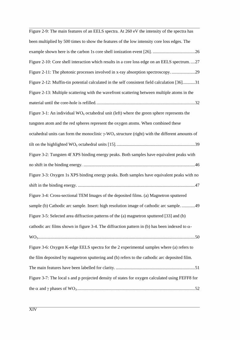
XIV
Figure 2-9: The main features of an EELS spectra. At 260 eV the intensity of the spectra has
been multiplied by 500 times to show the features of the low intensity core loss edges. The
example shown here is the carbon 1s core shell ionization event [26]. ...................................... 26
Figure 2-10: Core shell interaction which results in a core loss edge on an EELS spectrum. .... 27
Figure 2-11: The photonic processes involved in x-ray absorption spectroscopy. ..................... 29
Figure 2-12: Muffin-tin potential calculated in the self consistent field calculation [36]. .......... 31
Figure 2-13: Multiple scattering with the wavefront scattering between multiple atoms in the
material until the core-hole is refilled. ........................................................................................ 32
Figure 3-1: An individual WO6 octahedral unit (left) where the green sphere represents the
tungsten atom and the red spheres represent the oxygen atoms. When combined these
octahedral units can form the monoclinic -WO3 structure (right) with the different amounts of
tilt on the highlighted WO6 octahedral units [15]. ...................................................................... 39
Figure 3-2: Tungsten 4f XPS binding energy peaks. Both samples have equivalent peaks with
no shift in the binding energy. .................................................................................................... 46
Figure 3-3: Oxygen 1s XPS binding energy peaks. Both samples have equivalent peaks with no
shift in the binding energy. ......................................................................................................... 47
Figure 3-4: Cross-sectional TEM Images of the deposited films. (a) Magnetron sputtered
sample (b) Cathodic arc sample. Insert: high resolution image of cathodic arc sample. ............ 49
Figure 3-5: Selected area diffraction patterns of the (a) magnetron sputtered [33] and (b)
cathodic arc films shown in figure 3-4. The diffraction pattern in (b) has been indexed to -
WO3............................................................................................................................................. 50
Figure 3-6: Oxygen K-edge EELS spectra for the 2 experimental samples where (a) refers to
the film deposited by magnetron sputtering and (b) refers to the cathodic arc deposited film.
The main features have been labelled for clarity. ....................................................................... 51
Figure 3-7: The local s and p projected density of states for oxygen calculated using FEFF8 for
the and phases of WO3. ......................................................................................................... 52
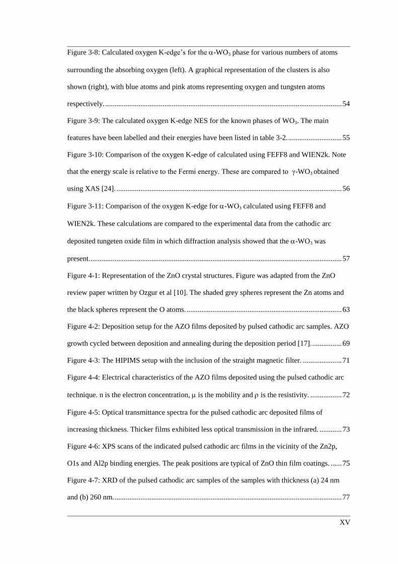
XV
Figure 3-8: Calculated oxygen K-edge‟s for the -WO3 phase for various numbers of atoms
surrounding the absorbing oxygen (left). A graphical representation of the clusters is also
shown (right), with blue atoms and pink atoms representing oxygen and tungsten atoms
respectively. ................................................................................................................................ 54
Figure 3-9: The calculated oxygen K-edge NES for the known phases of WO3. The main
features have been labelled and their energies have been listed in table 3-2. ............................. 55
Figure 3-10: Comparison of the oxygen K-edge of calculated using FEFF8 and WIEN2k. Note
that the energy scale is relative to the Fermi energy. These are compared to γ-WO3 obtained
using XAS [24]. .......................................................................................................................... 56
Figure 3-11: Comparison of the oxygen K-edge for -WO3 calculated using FEFF8 and
WIEN2k. These calculations are compared to the experimental data from the cathodic arc
deposited tungeten oxide film in which diffraction analysis showed that the -WO3 was
present. ........................................................................................................................................ 57
Figure 4-1: Representation of the ZnO crystal structures. Figure was adapted from the ZnO
review paper written by Ozgur et al [10]. The shaded grey spheres represent the Zn atoms and
the black spheres represent the O atoms. .................................................................................... 63
Figure 4-2: Deposition setup for the AZO films deposited by pulsed cathodic arc samples. AZO
growth cycled between deposition and annealing during the deposition period [17]. ................ 69
Figure 4-3: The HIPIMS setup with the inclusion of the straight magnetic filter. ..................... 71
Figure 4-4: Electrical characteristics of the AZO films deposited using the pulsed cathodic arc
technique. n is the electron concentration, is the mobility and is the resistivity. ................. 72
Figure 4-5: Optical transmittance spectra for the pulsed cathodic arc deposited films of
increasing thickness. Thicker films exhibited less optical transmission in the infrared. ............ 73
Figure 4-6: XPS scans of the indicated pulsed cathodic arc films in the vicinity of the Zn2p,
O1s and Al2p binding energies. The peak positions are typical of ZnO thin film coatings. ...... 75
Figure 4-7: XRD of the pulsed cathodic arc samples of the samples with thickness (a) 24 nm
and (b) 260 nm. ........................................................................................................................... 77
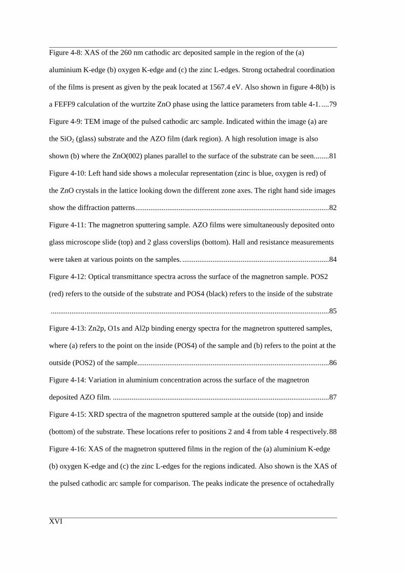
XVI
Figure 4-8: XAS of the 260 nm cathodic arc deposited sample in the region of the (a)
aluminium K-edge (b) oxygen K-edge and (c) the zinc L-edges. Strong octahedral coordination
of the films is present as given by the peak located at 1567.4 eV. Also shown in figure 4-8(b) is
a FEFF9 calculation of the wurtzite ZnO phase using the lattice parameters from table 4-1. .... 79
Figure 4-9: TEM image of the pulsed cathodic arc sample. Indicated within the image (a) are
the SiO2 (glass) substrate and the AZO film (dark region). A high resolution image is also
shown (b) where the ZnO(002) planes parallel to the surface of the substrate can be seen. ....... 81
Figure 4-10: Left hand side shows a molecular representation (zinc is blue, oxygen is red) of
the ZnO crystals in the lattice looking down the different zone axes. The right hand side images
show the diffraction patterns ....................................................................................................... 82
Figure 4-11: The magnetron sputtering sample. AZO films were simultaneously deposited onto
glass microscope slide (top) and 2 glass coverslips (bottom). Hall and resistance measurements
were taken at various points on the samples. .............................................................................. 84
Figure 4-12: Optical transmittance spectra across the surface of the magnetron sample. POS2
(red) refers to the outside of the substrate and POS4 (black) refers to the inside of the substrate
.................................................................................................................................................... 85
Figure 4-13: Zn2p, O1s and Al2p binding energy spectra for the magnetron sputtered samples,
where (a) refers to the point on the inside (POS4) of the sample and (b) refers to the point at the
outside (POS2) of the sample...................................................................................................... 86
Figure 4-14: Variation in aluminium concentration across the surface of the magnetron
deposited AZO film. ................................................................................................................... 87
Figure 4-15: XRD spectra of the magnetron sputtered sample at the outside (top) and inside
(bottom) of the substrate. These locations refer to positions 2 and 4 from table 4 respectively. 88
Figure 4-16: XAS of the magnetron sputtered films in the region of the (a) aluminium K-edge
(b) oxygen K-edge and (c) the zinc L-edges for the regions indicated. Also shown is the XAS of
the pulsed cathodic arc sample for comparison. The peaks indicate the presence of octahedrally
XVII
coordinated Al bonding, but are largely disordered structures. Also shown in figure 4-16(b) is a
FEFF9 calculation of the wurtzite ZnO phase using the lattice parameters from table 4-1........ 91
Figure 4-17: The deposited HIPIMS samples. The AZO films were deposited onto a glass
microscope slide (bottom) and 2 glass coverslips (top). Points of interest are labelled on the
image. ......................................................................................................................................... 93
Figure 4-18: Resistivity of the HIPIMS sample across the surface as measured by 4 point probe.
.................................................................................................................................................... 94
Figure 4-19: Optical transmittance spectra across the surface of the HIPIMS samples. POS1
(red) refers to the outside of the substrate and POS3 (black) refers to the inside of the substrate
.................................................................................................................................................... 95
Figure 4-20: Zn2p, O1s and Al2p binding energy spectra for the HIPIMS samples, where (a)
refers to the point on the inside (POS3) of the sample and (b) refers to the point at the outside
(POS1) of the sample .................................................................................................................. 97
Figure 4-21: XPS line scan of the Al2p peak across the surface of the HIPIMS sample from
position A to B. ........................................................................................................................... 98
Figure 4-22: Comparison of the HIPIMS XRD. Shown in the figure are the respective grain size
and Hall measurements for each of the samples. ........................................................................ 99
Figure 4-23: XAS of the indicated HIPIMS samples in the region of the (a) aluminium K-edge,
(b) oxygen K-edge and (c) zinc L-edges compared to the pulsed cathodic arc sample. Less
resolved peaks in the spectra relating to the centre of the HIPIMS samples is indicative of
increased disorder in the film. Also shown in figure 4-23(b) is a FEFF9 calculation of the
wurtzite ZnO phase using the lattice parameters from table 4-1. ............................................. 101
Figure 4-24: Optical transmittance spectra comparison between unfiltered HIPIMS (black) and
straight filtered HIPIMS (red) .................................................................................................. 103
Figure 4-25: Zn2p, O1s and Al2p binding energy spectra for the HIPIMS samples with and
without the straight line magnetic filter. where (a) refers to the filtered sample and (b) refers to
the unfiltered one. ..................................................................................................................... 104
XVIII
Figure 4-26: XPS line scan of the Al2p peak across the surface of the filtered HIPIMS sample
from position A to B. ................................................................................................................ 105
Figure 4-27: XRD comparison between the filtered HIPIMS sample and the HIPIMS sample.
.................................................................................................................................................. 106
Figure 4-28: XAS of the indicated HIPIMS samples in the region of the (a) aluminium K-edge,
(b) oxygen K-edge and (c) zinc L-edges. Less resolved peaks in the spectra relating to the
centre of the HIPIMS samples is indicative of increased disorder in the film. Also shown in
figure 4-23(b) is a FEFF9 calculation of the wurtzite ZnO phase using the lattice parameters
from table 4-1. ........................................................................................................................... 108
Figure 4-29: Comparison of the electrical properties for the techniques used to deposit the AZO
films. ......................................................................................................................................... 110
Figure 4-30: Comparison of transmission intensity for AZO films deposited by (a) magnetron
sputtering, (b) filtered HIPIMS, (c) HIPIMS and (d) cathodic arc deposition techniques........ 111
Figure 5-1: Schematic of HfO2 acting as a gate dielectric in a field effect transistor device .... 119
Figure 5-2: The three ambient pressure phases of HfO2 adapted from Zhao et. al [14]. .......... 120
Figure 5-3: XPS spectra of the HfO2 films with the indicated substrate biases in the region of
the hafnium 4f binding energy peaks. ....................................................................................... 124
Figure 5-4: XPS spectra of the HfO2 films with the indicated substrate bias‟s in the region of
the oxygen 1s binding energy peak. .......................................................................................... 125
Figure 5-5: SEM images of the HfO2 bias series with a (a) floating potential, (b) -100 V bias
and a (c) -500 V bias. ................................................................................................................ 127
Figure 5-6: AFM images of the bias series of HfO2 films deposited using FCVA deposited with
a (a) floating potential, (b) -100 V bias and a (c) -500 V bias. ................................................. 128
Figure 5-7: Bright field cross-sectional TEM images of the (a) sample deposited at floating
potential, (b) −100 V bias sample and the (c) −500 V bias sample. Note that the diffraction
pattern in (c) contains diffraction spots from the [011] zone axis of the Si substrate. The two
XIX
main diffraction rings indicated in (a) occur at d = 2.7 Å and d = 1.6 Å and can be indexed to
the (011) and a combination of the (120) and (211) reflections of monoclinic P21/c HfO2. .... 130
Figure 5-8: EELS spectra of the HfO2 films deposited at different substrate bias‟s compared to
that of a broadened monoclinic structure as calculated using the FEFF8 ab initio code. ......... 132
Figure 5-9: E-J characteristics of the HfO2 film deposited at floating potential. Films deposited
with a greater substrate bias sustained film damage and the breakdown characteristics couldn‟t
be determined. .......................................................................................................................... 133
Figure 5-10: XPS spectra of the Hafnium 4f peak for the HfOx films deposited at the
temperatures indicated. ............................................................................................................ 134
Figure 5-11: XPS spectra in the region of the oxygen 1s binding energy peak of the hafnium
oxide films deposited at the temperatures indicated ................................................................. 135
Figure 5-12: XRD patterns of the hafnium oxide films deposited with the indicated deposition
temperatures. The labelled peaks have been indexed either to the monoclinic or tetragonal
phases of HfO2 as shown in table 5-4. ...................................................................................... 137
Figure 5-13: X-TEM images of the HfO2 films prepared with substrate temperatures of (a)
room temperature, (b) 400 ºC and (c) 800 ºC. The HfO2 film is the dark region running down
the centre of each image, the silicon substrate is on the right hand side and the epoxy bonding
agent is on the left hand side. .................................................................................................... 139
Figure 5-14: SAED patterns of the film areas shown in figure 5-13, deposited with substrate
temperatures of (a) room temperature, (b) 400 ºC and (c) 800 ºC. The patterns have been
indexed to the monoclinic phase of HfO2. ................................................................................ 140
Figure 5-15: XAS in the vicinity of the oxygen K-edge of the HfO2 films deposited with the
indicated temperatures compared to a monoclinic powder standard. ....................................... 142
Figure 5-16: Comparison of the oxygen K-edge for the FEFF9 calculations of 3 phases of HfO2
compared to the 800ºC HfO2 sample and monoclinic powder standard. The spectra „FEFF9 –
Mix‟ refers to a 3:2 linear combination of the monoclinic phase and the tetragonal phase. .... 143
Figure 5-17: E-J characteristics measured from HfO2 films deposited using a FCVA with the
indicated substrate temperatures. .............................................................................................. 144
XX
List of Tables
Table 3-1: Details of the crystallography of the phases of WO3 and the method of formation of
the bulk crystal. Those marked with „Powder‟ in the formation method were a commercially
purchased polycrystalline powder of unspecified phase. ............................................................ 40
Table 3-2: The position (eV) of the main features in the experimental and calculated oxygen K-
edges. Note that the experimental and calculated values have been shifted so that the first NES
peak (A) aligns with previous XAS measurements of -WO3 [24]. ........................................... 58
Table 4-1: Crystallographic details of the main ZnO crystal structures. .................................... 63
Table 4-2: Pulsed arc electrical results. Electrical results were determined from the Hall Effect
measurements. ............................................................................................................................. 72
Table 4-3: Details for the atomic percentages of the pulsed arc deposited AZO films. ............. 76
Table 4-4: XRD of pulsed arc samples showing the film thickness, Bragg scattering angle,
FWHM of the XRD peak and the calculated crystal grain size. ................................................. 77
Table 4-5: Electrical measurements performed on the samples deposited by magnetron
sputtering. Highlighted cells refer to locations on the samples that are analysed later with other
techniques. NM refers to points where no measurement was possible. ...................................... 84
Table 4-6: Details of the XPS experiment on the magnetron sputtered samples ........................ 86
Table 4-7: Peak position and grain size analysis of the AZO samples deposited using magnetron
sputtering and HIPIMS. .............................................................................................................. 89
Table 4-8: Electrical characteristics for the HIPIMS sample. The positions refer to the points
shown in figure 4-17. Highlighted cells refer to locations on the samples that are analysed later
with other techniques .................................................................................................................. 93
XXI
Table 4-9: Details of the XPS experiment on the static HIPIMS sample. POS3 refers to the
inside of the sample, POS1 refers to the outside of the sample .................................................. 97
Table 4-10: Peak position and grain size analysis of the AZO samples deposited using
magnetron sputtering and HIPIMS. .......................................................................................... 100
Table 4-11: Electrical characteristics for the HIPIMS samples deposited both with and without
the inclusion of the straight magnetic filter. ............................................................................. 102
Table 4-12: Details of the XPS experiment on the static HIPIMS sample. POS3 refers to the
inside of the sample, POS1 refers to the outside of the sample ................................................ 104
Table 4-13: Peak position and grain size analysis of the AZO samples deposited using
magnetron sputtering and HIPIMS. .......................................................................................... 106
Table 4-14: Comparison of electrical properties for each of the listed deposition methods. Films
of similar thickness were chosen so that a fair comparison could be made. ............................ 110
Table 4-15: Comparison of microstructural properties of the deposited AZO films. ............... 112
Table 5-1: Lattice parameters of the ambient pressure phases calculated using GGA by Zhao et.
al [14] as well as their formation temperature. Also shown is the high pressure phase calculated
by Lowther et al. ....................................................................................................................... 120
Table 5-2: Atomic percentage of the HfO2 films with increasing substrate bias during
deposition determined using XPS. Each of the deposited films was found to be close to
stoichiometric HfO2. ................................................................................................................. 125
Table 5-3: Calculated atomic percentages within the HfO2 films rounded to the nearest percent.
.................................................................................................................................................. 135
Table 5-4: Details of the indexing of the XRD spectra shown in figure 2. All peaks could be
indexed either to the monoclinic or tetragonal phases of HfO2 using previously published lattice
parameters [14]. Note that multiple phases are shown for peaks „4‟ and „7‟ due to ambiguity in
the peak positions between the two phases. .............................................................................. 138
Table 5-5: The microstructures of the films determined using XRD and the electric field at
which the leakage current density exceeded 1 µAcm-2
. ............................................................ 144

XXII
Chapter 1: Introduction
1
Chapter 1
Introduction
Nanotechnology is one of the fastest growing areas in materials science, with billions of dollars
spent in the western economies to develop national nanotechnology initiatives and further
research into enhanced products that improve our lifestyles. Within the realm of
nanotechnology, the metal oxide group of materials plays an important role because of their
diverse range of properties and their outstanding performance for many applications. These
applications include capacitive devices, gas and bio sensor arrays, modulated refractive index
layers in optical coatings, solar cells and energy saving applications. The diversity of metal
oxide properties (and applications) arises from their complex atomic and electronic structures.
The reason for this complexity is the variety of oxidation states, coordination number,
symmetry, density, and stoichiometry giving rise to properties ranging from electrically
insulating to conducting and from optically opaque to transparent.
The focus of this thesis was the investigation of three different types of metal oxides, all of
which are technologically important. These are tungsten oxide, aluminium doped zinc oxide
(also known as aluminium zinc oxide or AZO) and hafnium oxide. Tungsten oxide and AZO
are members of a group of metal oxides known as transparent conducting oxides (TCO’s).
Normally conductive materials (such as metals) are opaque due to their large carrier
concentration, and insulating materials (such as glasses) are transparent. TCO’s are a unique
group of materials that combine the conductivity usually inherent in metals with the
transparency of glasses.
2
Tungsten oxide is a d0-transition metal oxide which exhibits many interesting optical, electrical
structural and defect properties. Interest in this TCO material begun back in 1837 when Wohler
observed an intense metal lustre in LiWO3 [1, 2]. Thinking that formation of metal alloys
caused this lustre, he named this set of materials ‘tungsten bronzes’. Considerable experimental
and theoretical work was performed by Mott [3], Sienko [4] and many others from the 1950’s
on tungsten bronzes because they are unusually conductive for oxidised materials [3-6]. Since
then in the mid 1960’s, thin film MoO3 and WO3 both have been studied to investigate
photochromism, an effect which causes thin films show reversible bleaching and
discolouration. This led to the discovery of the electrochromic (EC) effect in highly disordered
films.
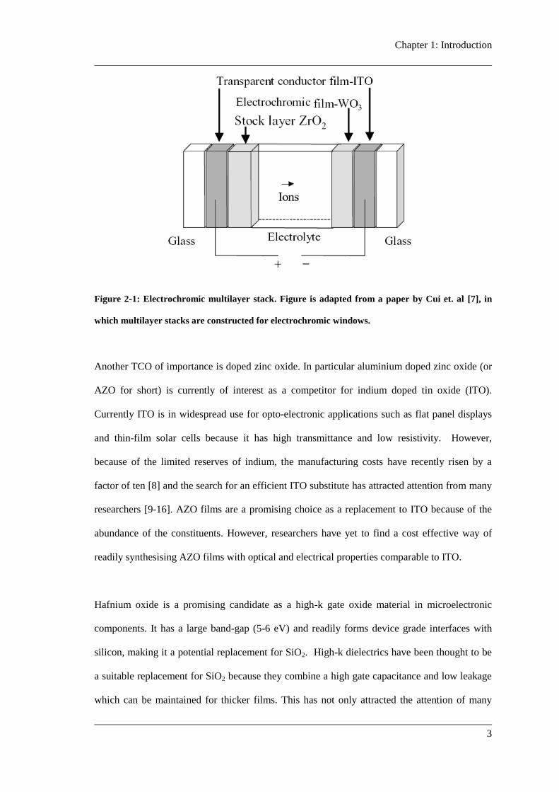
Soon ‘thin film sandwiches’ were being constructed, whereby a multilayer film stack is
synthesised and has been shown to exhibit a reversible change in colouration. Figure 2-1 shows
an example of WO3 used in a multilayer stack for electrochromic windows [7]. The EC effect
was originally demonstrated using semi solid state devices were used with a liquid electrolyte,
but a much more practical solution is to use a multilayer stack film to construct a full solid state
device. An example of this structure is M-SiO-WO3-TCO, which has been modified to include
other transition metal oxides, and has since been studied extensively. Although studied for
some time, there is still considerable interest in investigating the structure-property
relationships in tungsten oxides.
Chapter 1: Introduction
3
Figure 2-1: Electrochromic multilayer stack. Figure is adapted from a paper by Cui et. al [7], in
which multilayer stacks are constructed for electrochromic windows.
Another TCO of importance is doped zinc oxide. In particular aluminium doped zinc oxide (or
AZO for short) is currently of interest as a competitor for indium doped tin oxide (ITO).
Currently ITO is in widespread use for opto-electronic applications such as flat panel displays
and thin-film solar cells because it has high transmittance and low resistivity. However,
because of the limited reserves of indium, the manufacturing costs have recently risen by a
factor of ten [8] and the search for an efficient ITO substitute has attracted attention from many
researchers [9-16]. AZO films are a promising choice as a replacement to ITO because of the
abundance of the constituents. However, researchers have yet to find a cost effective way of
readily synthesising AZO films with optical and electrical properties comparable to ITO.
Hafnium oxide is a promising candidate as a high-k gate oxide material in microelectronic
components. It has a large band-gap (5-6 eV) and readily forms device grade interfaces with
silicon, making it a potential replacement for SiO2. High-k dielectrics have been thought to be
a suitable replacement for SiO2 because they combine a high gate capacitance and low leakage
which can be maintained for thicker films. This has not only attracted the attention of many
4
research groups [17-21], but is also being studied by the Intel Corporation for use as a
complementary metal oxide semiconductor in transistors [22, 23]. It remains a challenge to
indentify the most effective method of synthesising HfO2 films with high dielectric constant
and low leakage current.
It is clear that tungsten oxide, AZO and hafnium oxide are technologically important materials.
However, for these materials to fulfil their potential, precise control over their synthesis is
needed. Since most applications require thin films, methods for synthesis are required which
allow the deposition of high quality films with precise thicknesses. In addition, depending on
the deposition method used, different microstructure can result leading to vastly different
electrical and optical properties. It has been shown, for example, that depending on deposition
method ZnO films can be grown to be spherically shaped, lenticular or columnar [13, 24, 25].
Since electrical and optical properties of materials are dependant on the microstructure, in order
to fully optimise a material for use in industry, their structure must be understood on an atomic
level. Therefore, methods which are capable of studying structure at high spatial resolution are
critical. For this reason, this thesis employs electron microscopy, diffraction and spectroscopy
techniques which are capable of accurately investigating the atomic level, structure and
bonding.
This thesis synthesises thin films with a process known as physical vapour deposition (PVD) in
which a coating is deposited from a plasma of its constituent elements. Several different PVD
methods are available which differ in the way they produce the plasma. For example, sputtering
methods produce a plasma by bombarding a target with inert gas ions (usually Ar), whereas in a
filtered cathodic vacuum arc (FCVA) the plasma is generated by applying a high current to a
conducting cathode. These plasmas differ considerably in their nature and this can lead to
considerable differences in the microstructure of the deposited films. For example, in
conventional sputtering, films are formed mainly by low energy neutrals while in the cathodic
arc, deposition occurs from energetic ions. It is therefore important that the relationship
Chapter 1: Introduction
5
between synthesis method and the resulting microstructure and properties of a particular type of
film be investigated. By properly understanding the strengths and weaknesses of the deposition
techniques, it is possible to extend this knowledge to other fields and enhance the properties of
other thin films.
The specific aims of this thesis are:
to study tungsten oxide thin films deposited by two very different deposition techniques
– pulsed magnetron sputtering and pulsed cathodic arc so that the relationship between
deposition conditions and resulting microstructure can be determined.
to investigate AZO coatings prepared using pulsed cathodic arc, pulsed magnetron
sputtering and high power impulse magnetron sputtering (HIPIMS) in order to
determine the optimum conditions under which films can be prepared with high optical
transparency and good electrical performance.
to undertake a thorough investigation of hafnium oxide coatings prepared using a
filtered cathodic vacuum arc. An important aspect of the study was to find a link
between the type of structure of the deposited film and its breakdown voltage so that
the electrical properties can be optimised for future use as a gate dielectric in
microprocessor applications.
This thesis is divided into several chapters. Chapter 2 outlines the background theory,
describing both the deposition methods used to synthesise the thin film coatings and the
techniques used to study them. Chapters 3, 4 and 5 present the main results of the investigation
of the three metal oxide coatings outlined in the aims above. Chapter 6 provides a summary on
the work presented in this thesis as well as some future work to be explored.
6
The major outcomes of this thesis include:
Tungsten oxide films deposited using pulsed cathodic arc and pulsed magnetron
sputtering exhibit very different microstructures. Films deposited using pulsed cathodic
arc were ordered and exhibited a phase which is usually only observed at high
temperatures, while pulsed magnetron sputtering produced films that were highly
disordered.
A comparison of AZO films prepared using several physical vapour deposition
techniques found that films deposited using pulsed cathodic arc displayed the best
electrical properties.
Non-uniformity in magnetron sputtered AZO coatings, which had previously been
thought to be due to in situ oxygen ion damage during film growth, was confirmed by
using a novel magnetic filter to remove these ions during deposition. The magnetic
filter was also found to increase the deposition rate in HIPIMS, potentially overcoming
the major limitation of this technique which is a low deposition rate.
Hafnium oxide films deposited at room temperature using an FCVA display a
disordered microstructure and exhibit good breakdown characteristics. Those deposited
at elevated temperatures have improved crystallinity, however, the breakdown
characteristics are compromised, supporting the proposition that disordered hafnium
oxide films exhibit the best electrical breakdown properties.
Throughout this thesis, ab initio calculations were found to be extremely useful for
simulating near-edge structure of metal oxides and help identify changes in local
bonding and microstructure.
Chapter 1: Introduction
7
1.1 Bibliography
1. Raubenheimer, O., Friedrich wöhler and the centenary of synthesis. Journal of the
American Pharmaceutical Association, 1928. 17(10): p. 973-980.
2. Deb, S.K., Opportunities and challenges in science and technology of WO3 for
electrochromic and related applications. Solar Energy Materials and Solar Cells, 2008.
92(2): p. 245-258.
3. Mott, N.F., The degenerate electron gas in tungsten bronzes and in highly doped
silicon. Philosophical Magazine, 1977. 35(1): p. 111 - 128.
4. Sienko, M.J. and S.M. Morehouse, Electrical and Magnetic Properties of Potassium
Tungsten Bronze and Rubidium Tungsten Bronze. Inorganic Chemistry, 1963. 2(3): p.
485-489.
5. Straumanis, M.E. and S.S. Hsu, The Lithium Tungsten Bronzes. Journal of the
American Chemical Society, 1950. 72(9): p. 4027-4030.
6. Weller, P.F., B.E. Taylor, and R.L. Mohler, Crystal preparation of doped sodium
tungsten bronze. Materials Research Bulletin, 1970. 5(6): p. 465-476.
7. Cui, H.N., M.F. Costa, V. Teixeira, I. Porqueras, and E. Bertran, Electrochromic
coatings for smart windows. Surface Science Proceedings of the 7th International
Conference on Nanometer-Scale Science and Technology and the 21st European
Conference on Surface Science, 2003. 532-535: p. 1127-1131.
8. Minami, T., Present status of transparent conducting oxide thin-film development for
Indium-Tin-Oxide (ITO) substitutes. Thin Solid Films, 2008. 516(17): p. 5822-5828.
9. Anders, A., S.H.N. Lim, K.M. Yu, J. Andersson, J. Rosén, M. McFarland, and J.
Brown, High quality ZnO:Al transparent conducting oxide films synthesized by pulsed
filtered cathodic arc deposition. Thin Solid Films, 2010. 518(12): p. 3313-3319.
10. Dasgupta, N.P., S. Neubert, W. Lee, O. Trejo, J.-R. Lee, and F.B. Prinz, Atomic Layer
Deposition of Al-doped ZnO Films: Effect of Grain Orientation on Conductivity.
Chemistry of Materials, 2010. 22(16): p. 4769-4775.
11. Deng, Z., C. Huang, J. Huang, M. Wang, H. He, H. Wang, and Y. Cao, Effects of Al
content on the properties of ZnO:Al films prepared by
Al<sub>2</sub>O<sub>3</sub> and ZnO co-sputtering.
Journal of Materials Science: Materials in Electronics, 2010. 21(10): p. 1030-1035.
12. Fang, G. and et al., Magnetron sputtered AZO thin films on commercial ITO glass for
application of a very low resistance transparent electrode. Journal of Physics D:
Applied Physics, 2002. 35(23): p. 3096.
13. Lim, D.G., D.H. Kim, J.K. Kim, O. Kwon, K.J. Yang, K.I. Park, B.S. Kim, S.W. Lee,
M.W. Park, and D.J. Kwak, Improved electrical properties of ZnO:Al transparent
conducting oxide films using a substrate bias. Superlattices and Microstructures, 2006.
39(1-4): p. 107-114.
14. Saarenpää, H., T. Niemi, A. Tukiainen, H. Lemmetyinen, and N. Tkachenko,
Aluminum doped zinc oxide films grown by atomic layer deposition for organic
photovoltaic devices. Solar Energy Materials and Solar Cells, 2010. 94(8): p. 1379-
1383.
15. Tsujino, J., N. Homma, T. Sugawara, I. Shimono, and Y. Abe, Preparation of Al-doped
ZnO thin films by RF thermal plasma evaporation. Thin Solid Films, 2002. 407(1-2): p.
86-91.
16. Xu, J., H. Wang, L. Yang, M. Jiang, S. Wei, and T. Zhang, Low temperature growth of
highly crystallized ZnO:Al films by ultrasonic spray pyrolysis from acetylacetone salt.
Materials Science and Engineering: B, 2010. 167(3): p. 182-186.
17. Afanas'ev, V.V., A. Stesmans, and W. Tsai, Determination of interface energy band
diagram between (100)Si and mixed Al--Hf oxides using internal electron
photoemission. Applied Physics Letters, 2003. 82(2): p. 245-247.
8
18. Nguyen, N.V., A.V. Davydov, D. Chandler-Horowitz, and M.M. Frank, Sub-bandgap
defect states in polycrystalline hafnium oxide and their suppression by admixture of
silicon. Applied Physics Letters, 2005. 87(19): p. 192903-3.
19. Preisler, E.J., S. Guha, M. Copel, N.A. Bojarczuk, M.C. Reuter, and E. Gusev,
Interfacial oxide formation from intrinsic oxygen in W--HfO2 gated silicon field-effect
transistors. Applied Physics Letters, 2004. 85(25): p. 6230-6232.
20. Yan, Z.J., R. Xu, Y.Y. Wang, S. Chen, Y.L. Fan, and Z.M. Jiang, Thin HfO2 films
grown on Si(100) by atomic oxygen assisted molecular beam epitaxy. Applied Physics
Letters, 2004. 85(1): p. 85-87.
21. Yu, H.Y., M.F. Li, B.J. Cho, C.C. Yeo, M.S. Joo, D.L. Kwong, J.S. Pan, C.H. Ang, J.Z.
Zheng, and S. Ramanathan, Energy gap and band alignment for (HfO2)x(Al2O3)1 - x on
(100) Si. Applied Physics Letters, 2002. 81(2): p. 376-378.
22. Chau, R., J. Brask, S. Datta, G. Dewey, M. Doczy, B. Doyle, J. Kavalieros, B. Jin, M.
Metz, A. Majumdar, and M. Radosavljevic, Application of high- gate dielectrics and
metal gate electrodes to enable silicon and non-silicon logic nanotechnology.
Microelectronic Engineering, 2005. 80: p. 1-6.
23. Chau, R., S. Datta, M. Doczy, J. Kavalieros, and M. Metz, Gate Dielectric Scaling for
High-Performance CMOS: from SiO2 to High-, in Extended Abstracts of International
Workshop on Gate Insulator (IWGI). November 2003, pp. 124-126: Tokyo, Japan.
24. Lu, J.G., Z.Z. Ye, Y.J. Zeng, L.P. Zhu, L. Wang, J. Yuan, B.H. Zhao, and Q.L. Liang,
Structural, optical, and electrical properties of (Zn,Al)O films over a wide range of
compositions. Journal of Applied Physics, 2006. 100(7): p. 073714-11.
25. Schuler, T. and M.A. Aegerter, Optical, electrical and structural properties of sol gel
ZnO:Al coatings. Thin Solid Films, 1999. 351(1-2): p. 125-131.

Chapter 2: Background
9
Chapter 2
Background
This chapter describes the techniques used to deposit the metal oxide films and explains why
they were selected. Following this, the experimental methods used to characterise the thin films
are presented. Finally, the ab initio codes which was used to predict the fine structure on
absorption edges measured using electron energy loss and x-ray absorption spectroscopy are
described. This calculated fine structure was found to be particularly useful for helping to
identify phases in the several of the metal oxides of interest in this thesis.
10
2.1 Metal oxide deposition
For the work outlined in this thesis, metal oxide thin films were deposited using a variety of
techniques. In the following sections, details of these deposition techniques are presented.
2.1.1 Cathodic arc deposition
In this deposition technique, a conducting cathode is kept under vacuum and is connected to a
high current (20-200 A), low voltage power (~20 V) supply. After being initiated by striking
the cathode with an earthed trigger, a plasma stream is formed. This plasma stream expands and
is directed away from the cathode towards the substrate material to form a thin film. The
mechanisms for this plasma deposition process are still hotly debated [1-4], but one theory
suggests that the high current forms localised intense electric fields and explosive field
emission of electrons [5]. This field emission causes local heating in the cathode, and in turn
thermally emitted electrons are also released. The constant emission of electrons in this way
forms a positive feedback loop, and thermal runaway occurs forming microscopic non-
stationary regions known as „cathode spots‟. These microscopic cathode spots have extremely
high current density, power density and plasma density. Over time the plasma spots increase in
size, which in turn reduces the current density and the voltage at the spot will drop. The rapid
heating of the material in this localised region also reduces the conductivity, making it less
favourable for the spot to remain stationary. This extinguishes the plasma spot at its current
location and a new spot will form with the same current density in a new location, giving rise to
a near continuous plasma emission. The plasma expanding from the cathode contains charged
ions (of kinetic energy approximately 18-150 eV), and due to the explosive nature of the
process the plasma stream also contains macroparticles and neutral atoms. Macroparticles are
undesirable since they can degrade film quality.
Chapter 2: Background
11
2.1.2 Filtered cathodic vacuum arc (FCVA) deposition
For the removal of macroparticles, the FCVA was developed by Akensov et al in 1978 [6]. In
this design, a 90º toroidal magnetic filter was used to direct the plasma stream from the cathode
to the substrate. When using a magnetic field in this manner, the plasma stream follows the
filter around the 90º bend because it is highly charged. Any macroparticles and neutral atoms
are unaffected by the field, thus will continue in their original trajectory and are filtered out.
Further improvements to the magnetic filter have since been made. The FCVA located at RMIT
University (used in this study, shown in figure 2-1) uses an off-plane double bend magnetic
filter, first developed by Shi et al [1], to more effectively remove macroparticles.
Figure 2-2 shows a schematic of the FCVA at RMIT University. The cathode is water cooled to
prevent heating damage to nearby components, and is rotated during deposition to further
randomise the location at which the cathode spots appear so that even wear of the cathode
surface is achieved. The plasma produced at the cathode is directed through an off plane double
bend magnetic filter towards the sample holder holding the substrate. The sample holder is
connected to a DC power supply so that a controllable bias can be supplied to the substrate to
increase the deposition energy of the plasma. The deposition system was pumped by a turbo-
molecular pump backed by a scroll pump.
12
Figure 2-1: The FCVA deposition system at RMIT University (Melbourne, Australia) used for
these experiments in this thesis. Note the double bend filter on the right. The plasma is generated
near the cathode and directed through the off-plane double bend magnetic filter to the sample
holder and substrate.
For the energetic deposition of metal oxides in this work, the films were grown in the presence
of background gases. During the plasma production process, a mixture of argon and oxygen gas
was bled into the chamber. The oxygen gas is present to react with the metal film as it grows,
and the argon gas is present to encourage plasma stability. Due to the nature of cathodic arc
deposition, a conductive cathode is required, which can be “poisoned” when oxygen is present
due to the build up of an insulating layer on the surface of the cathode. To help combat this, the
argon and oxygen gases were bled into the chamber at two different locations. The oxygen gas
was bled into the deposition chamber near to the substrate and the argon was bled into the
chamber near to the cathode so that it provides stability to the plasma, as well as providing
Chapter 2: Background
13
upwards pressure in the bottom half of the chamber, reducing the amount of oxygen gas
reacting with the cathode.
Figure 2-2: Schematic of the continuous FCVA system (not to scale).
If the substrate is electrically grounded during film deposition, then the ions within the plasma
will deposit onto the substrate with their original ion energy. It is possible to modify the energy
of the depositing ions by placing an electrical bias onto the substrate to either accelerate the
ions (with a negative bias) or decelerate them (positive bias) [7, 8]. The equation that describes
the ion energy during deposition is:
Equation 2-1: Energy of ions in a plasma during film deposition
14
where Ei is the energy of the ions reaching the substrate, q is the charge state of the ions, Vp is
the plasma potential, Vb is the substrate potential and Eo is the original energy of the plasma. It
has been shown [8, 9] that by modifying the substrate bias (and hence the ion energy), it is
possible to change not only the microstructure of the film, but its physical properties such as
hardness, density and optical properties. Also possible in FCVA deposition is the growth of
films with increased substrate temperatures. This was performed using a specimen stage and
controller. Generally, increasing the substrate temperature increases the surface mobility of the
deposited atoms, giving them enough energy to find lower energy states and therefore more
ordered films result.
2.1.3 Pulsed cathodic arc deposition
In addition to conventional cathodic arc deposition a pulsed cathodic arc was used to deposit
films (see figure 2-3). In a pulsed cathodic arc system much higher deposition rates are
achieved by controlling the current to the cathode with a pulse generator. Doing so allows for a
much higher power density and the system will cool in between pulses. As shown
schematically in figure 2-4 the substrate, macroparticle filter and plasma source are connected
to a master pulse generator. This controls the entire system so that the high voltage pulses
within each of the components will only be applied during the short deposition periods.
Chapter 2: Background
15
Figure 2-3: The pulsed arc system located at Lawrence Berkeley National Labs (Berkeley, USA)
Figure 2-4: Schematic of the pulse generation systems used with the pulsed cathodic arc setup [10].
For the pulsed cathodic arc experiments, a 90º single bend macroparticle filter was used to
remove the macroparticles and low energy neutrals, as well as direct the plasma towards the
16
substrate. The substrate was mounted onto the sample holder which rotates during the
deposition to promote even coverage.
2.1.4 Magnetron sputtering
Magnetron sputtering is a highly regarded thin film deposition technique whose origins go back
to the introduction of the planar magnetron by J. S Chapin in 1974 [11, 12]. It is used by many
research groups for the development of advanced coatings and is also in widespread use in
industry for large scale coating of high quality films. In a conventional sputtering process, inert
gas ions (such as argon) are accelerated towards a negatively biased target material. This target
contains at least one of the constituents to be deposited onto the substrate. When the target is
sputtered, the material to be deposited and secondarily electrons are ejected and form a thin
film on the substrate placed nearby within the vacuum. It is also possible to deposit compounds
such as metal oxides by introducing another gas into the chamber. This process is often referred
to as reactive sputtering. A schematic of the magnetron sputtering process is shown in figure 2-
5.
Figure 2-5: Schematic of a conventional magnetron sputtering system. Shown in the image are the
field lines trapping the secondary electrons to form more ionisation events, increasing the
deposition rate.
+
N S S
+
Directed neutral flux of
target atoms
Normal
sputtering
power
supply
Substrate
Growing film Inert Gas
inlet
Low voltage
sheath
Target
Chapter 2: Background
17
In magnetron sputtering the target is mounted upon a series of negatively biased magnetrons
which are used to attract the positive ions [11]. Inclusion of the ring magnets traps the
secondary electrons within the magnetic field allowing for more ionisation events to occur,
further increasing the deposition rate of the target material.
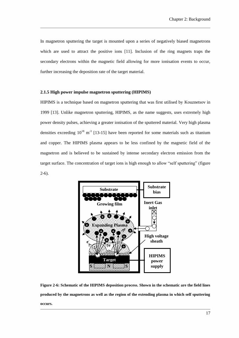
2.1.5 High power impulse magnetron sputtering (HIPIMS)
HIPIMS is a technique based on magnetron sputtering that was first utilised by Kouznetsov in
1999 [13]. Unlike magnetron sputtering, HIPIMS, as the name suggests, uses extremely high
power density pulses, achieving a greater ionisation of the sputtered material. Very high plasma
densities exceeding 1018
m-3
[13-15] have been reported for some materials such as titanium
and copper. The HIPIMS plasma appears to be less confined by the magnetic field of the
magnetron and is believed to be sustained by intense secondary electron emission from the
target surface. The concentration of target ions is high enough to allow “self sputtering” (figure
2-6).
Figure 2-6: Schematic of the HIPIMS deposition process. Shown in the schematic are the field lines
produced by the magnetrons as well as the region of the extending plasma in which self sputtering
occurs.
+
N S S
+
Expanding Plasma
HIPIMS
power
supply
Substrate
Growing film Inert Gas
inlet
High voltage
sheath
Target
+
+ +
+
+ + +
+
+
e-
e-
e-
Substrate
bias
18
A universal problem in HIPIMS, for both non reactive and reactive processes, is a low
deposition rate. A recent report has shown that ions can be more efficiently directed towards the
substrate in the so called “unbalanced” magnetron which uses a magnetic field with open lines
of force that connect the substrate to the target [16, 17]
2.2 Experimental Analysis Methods
2.2.1 Scanning electron microscopy (SEM)
SEM images were obtained using a FEI Nova NanoSEM field emission SEM in high vacuum
mode with a spot size of 3.5 nm and an accelerating voltage of 20kV. Carbon strapping was run
from the surface of the samples to the stub (earth) to minimise any possible charging effects on
the sample surface during image acquisition.
2.2.2 Atomic force microscopy (AFM)
AFM is a technique which can be used to provide very high resolution surface profiles of a
sample. It can be used to determine the RMS roughness of a surface and give topographic
information. AFM was performed using a Veeco Dimension 3100 AFM operated in tapping
mode over an area of 500m x 500m to determine the RMS roughness and defect density of
the samples.
2.2.2 X-ray diffraction (XRD)
XRD is a technique which takes advantage of Bragg diffraction, in which x-rays of a known
wavelength are used to probe a sample. XRD studies were carried out on a Bruker D8
ADVANCE wide-angle diffractometer, using a graphite-monochromated Cu K source of
wavelength = 1.5406 Å. Data was collected with a scan range of 2= 10–90, a step size of
0.02 and a count rate of 2s per step.
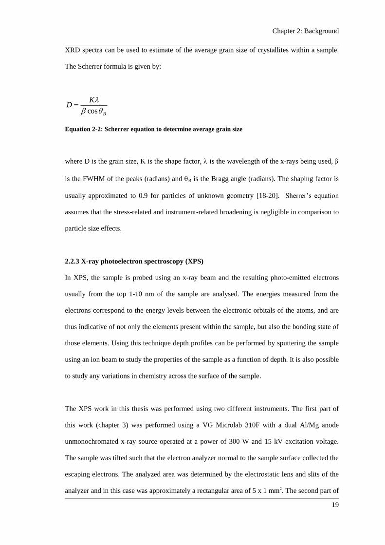
Chapter 2: Background
19
XRD spectra can be used to estimate of the average grain size of crystallites within a sample.
The Scherrer formula is given by:
B
KD
cos
Equation 2-2: Scherrer equation to determine average grain size
where D is the grain size, K is the shape factor, is the wavelength of the x-rays being used,
is the FWHM of the peaks (radians) and B is the Bragg angle (radians). The shaping factor is
usually approximated to 0.9 for particles of unknown geometry [18-20]. Sherrer‟s equation
assumes that the stress-related and instrument-related broadening is negligible in comparison to
particle size effects.
2.2.3 X-ray photoelectron spectroscopy (XPS)
In XPS, the sample is probed using an x-ray beam and the resulting photo-emitted electrons
usually from the top 1-10 nm of the sample are analysed. The energies measured from the
electrons correspond to the energy levels between the electronic orbitals of the atoms, and are
thus indicative of not only the elements present within the sample, but also the bonding state of
those elements. Using this technique depth profiles can be performed by sputtering the sample
using an ion beam to study the properties of the sample as a function of depth. It is also possible
to study any variations in chemistry across the surface of the sample.
The XPS work in this thesis was performed using two different instruments. The first part of
this work (chapter 3) was performed using a VG Microlab 310F with a dual Al/Mg anode
unmonochromated x-ray source operated at a power of 300 W and 15 kV excitation voltage.
The sample was tilted such that the electron analyzer normal to the sample surface collected the
escaping electrons. The analyzed area was determined by the electrostatic lens and slits of the
analyzer and in this case was approximately a rectangular area of 5 x 1 mm2. The second part of
20
this work (chapters 4 and 5) were performed using a Thermo Scientific K-Alpha Spectrometer
with an Al anode x-ray source. The spot size for measurements was ~400m and a flood gun
was utilised to remove the possibility of sample charging during analysis. Depth profiles were
performed to remove surface contaminants with a 500eV Ar ion beam with a low sputter
current so as to not damage the sample during analysis.
In addition to collecting spectra in the region of the oxygen 1s, carbon 1s and metal bonding
peaks, broad survey spectra were also collected to check for the possibility of impurities within
the films. Samples were argon ion sputter cleaned before measurements were performed to
remove any surface contaminants. Since cleaning may alter the bonding of the sample, care
must be taken when analysing bond information. Gaussian peaks were fitted to these binding
energy spectra using the Thermo Avantage software, the peak area was calculated, normalised
and sensitivity factors of the corresponding peaks were applied to determine the composition.
2.2.4 Optical transmission
Optical transmission spectra were performed on the AZO films to determine their suitability as
a transparent conducting oxide (TCO). Transmittance measurements were performed using a
Perkin-Elmer Lambda 19 and 950 by spectrophotometry in the wavelength range of 200-2500
nm. The sample must be deposited onto a transparent substrate so that the transmittance of the
film can be determined. In a spectrophotometry experiment, a light source is shone onto a
monochromator, a device with a diffraction grating used to select a particular wavelength. This
monochomated light then passes through the sample and then has its intensity measured using a
light sensitive detector. By cycling the monochromator through a variety of wavelengths, the
transparency of the films can be determined as a function of wavelength.
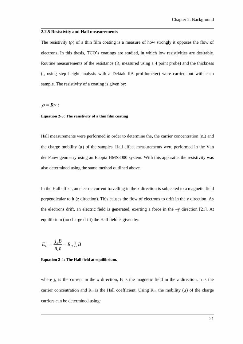
Chapter 2: Background
21
2.2.5 Resistivity and Hall measurements
The resistivity () of a thin film coating is a measure of how strongly it opposes the flow of
electrons. In this thesis, TCO‟s coatings are studied, in which low resistivities are desirable.
Routine measurements of the resistance (R, measured using a 4 point probe) and the thickness
(t, using step height analysis with a Dektak IIA profilometer) were carried out with each
sample. The resistivity of a coating is given by:
tR
Equation 2-3: The resistivity of a thin film coating
Hall measurements were performed in order to determine the, the carrier concentration (ne) and
the charge mobility () of the samples. Hall effect measurements were performed in the Van
der Pauw geometry using an Ecopia HMS3000 system. With this apparatus the resistivity was
also determined using the same method outlined above.
In the Hall effect, an electric current travelling in the x direction is subjected to a magnetic field
perpendicular to it (z direction). This causes the flow of electrons to drift in the y direction. As
the electrons drift, an electric field is generated, exerting a force in the –y direction [21]. At
equilibrium (no charge drift) the Hall field is given by:
BjRen
BjE xH
e
xH
Equation 2-4: The Hall field at equilibrium.
where jx is the current in the x direction, B is the magnetic field in the z direction, n is the
carrier concentration and RH is the Hall coefficient. Using RH, the mobility () of the charge
carriers can be determined using:
22
ene
1
Equation 2-5: Mobility of the charge carriers as a function of the resistivity
2.2.6 Breakdown voltage
The breakdown characteristics of a dielectric thin film are related to the potential at which
current flows through it. A requirement for a dielectric film is to able to hold charge without
leakage currents due to crystal grain boundaries and quantum tunneling [22-25]. The higher the
breakdown field of a metal oxide semiconductor device, the better the performance as a
transistor. The electrical breakdown characteristics of the films were measured using
lithographically defined NiCr contact pads on the surface of the films, a probing station and a
programmable semiconductor parameter. The E(J) (leakage) characteristics were obtained
using a programmable voltage ramping source and a PC-interfaced digital multimeter. Film
thickness measurements (required to calculate the electric-field from applied voltage) were
performed using a surface profiler.
2.2.7 Transmission electron microscopy (TEM) sample preparation
Cross sectional TEM (X-TEM) samples were prepared by first mechanical polishing with a
tripod polisher and then further thinning with argon ion beams. X-TEM samples allow for the
study of films as a function of depth, allowing the microstructure and electronic structure of the
films to be thoroughly explored.
The first step for mechanically thinning the samples involves cleaving 3mm x 1mm strips from
the samples and preparing strips of blank silicon in the same manner. The pieces are then
affixed together using epoxy glue as shown in figure 2-7a. This sandwich structure is affixed to
a polished silicon flat on a quartz stub (figure 2-7b) and is then mechanically polished on
increasingly fine diamond paper (30m 9m3m1m) until the sample is less than 1m
in thickness (figure 2-7c). An oval shaped copper grid with a section cut out of it is then affixed
Chapter 2: Background
23
to the sample using epoxy glue. The X-TEM sample is then cut out of the structure using a
razor blade (figure 2-7d) and lifted from the structure by soaking it in acetone.
Figure 2-7: Mechanical polishing X-TEM preparation thinning process. This figure has been
adapted from Desmond Lau’s thesis 2009 [26].
For ion beam thinning of the sample the copper grid with sample attached is placed into the
precision ion polishing system (PIPS, Gatan Model 691) where the sample is ion beam thinned
until a region surrounding the thin film is less than 100nm in thickness (electron transparent).
X- TEM samples were also prepared using a JEOL ion slicer. Samples were prepared by first
epoxy gluing a protective capping material (eg. a microscope coverslip or silicon) on top of the
sample of interest. This was then polished down in cross-section to approximately 100 m in
thickness and cut into 2.8 mm x 1 mm pieces. After mechanical polishing, the sample was
placed into the ion slicer. An ion gun is positioned above the specimen and a thin masking belt
is used to protect the centre region by acting as a sacrificial shield. During milling the sample
rocks back and forth parallel to the masking belt to provide even thinning. There are two ion
beam milling steps, the first step was a basic thinning of the sample to make a thin channel
24
down the centre. The second step involves setting the ion gun to thin the region of interest at a
selected angle until a hole appears in the specimen.
2.2.8 TEM and selected area electron diffraction (SAED)
TEM is one of the major analytical techniques employed in this thesis to determine the
microstructure of the metal oxide thin films. Analysis was performed on either a JEOL 2010
TEM or a JEOL2100F TEM, both fitted with a Gatan imaging filter (GIF) spectrometers. A
GIF not only allows the collection of electron energy loss spectroscopy spectra but can also be
used to collect energy filtered TEM images [27, 28].
Figure 2-8 shows a basic schematic of the TEM system. Included are ray diagrams to show how
the electrons pass through the TEM to provide high resolution images (Figure 2-8a) and
diffraction (Figure 2-8b). Electrons are generated from a LaB6 filament, accelerated to 200kV
and then pass through a series of magnetic filters (depicted as ovals in figure 2-8). Images are
formed when the flux of electrons are focussed onto the specimen using the condenser lens
system, following this the objective lens focuses the image onto the 1st image plane and is thus
focussed onto the phosphor screen using the projector lens system. For diffraction, the
condenser lens system is used to project a parallel beam through the specimen. In diffraction
mode, the projector lens system focuses on the back focal plane of the objective lens, producing
a diffraction pattern instead of an image on the viewing screen. Diffraction patterns give a
reciprocal space representation of the crystal planes within a film, where the spots appear
perpendicular to the planes. Using the distance from the primary beam to a diffraction spot, the
d-spacing can be calculated using Bragg‟s law [29]. In a disordered sample the crystal planes
are in many directions, thus the diffraction pattern appears as ring patterns where the d spacings
and can be deduced in a similar way.
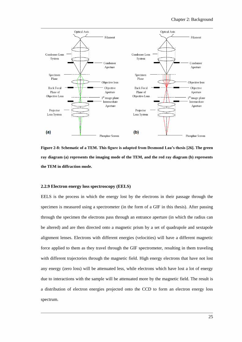
Chapter 2: Background
25
Figure 2-8: Schematic of a TEM. This figure is adapted from Desmond Lau’s thesis [26]. The green
ray diagram (a) represents the imaging mode of the TEM, and the red ray diagram (b) represents
the TEM in diffraction mode.
2.2.9 Electron energy loss spectroscopy (EELS)
EELS is the process in which the energy lost by the electrons in their passage through the
specimen is measured using a spectrometer (in the form of a GIF in this thesis). After passing
through the specimen the electrons pass through an entrance aperture (in which the radius can
be altered) and are then directed onto a magnetic prism by a set of quadrupole and sextapole
alignment lenses. Electrons with different energies (velocities) will have a different magnetic
force applied to them as they travel through the GIF spectrometer, resulting in them traveling
with different trajectories through the magnetic field. High energy electrons that have not lost
any energy (zero loss) will be attenuated less, while electrons which have lost a lot of energy
due to interactions with the sample will be attenuated more by the magnetic field. The result is
a distribution of electron energies projected onto the CCD to form an electron energy loss
spectrum.
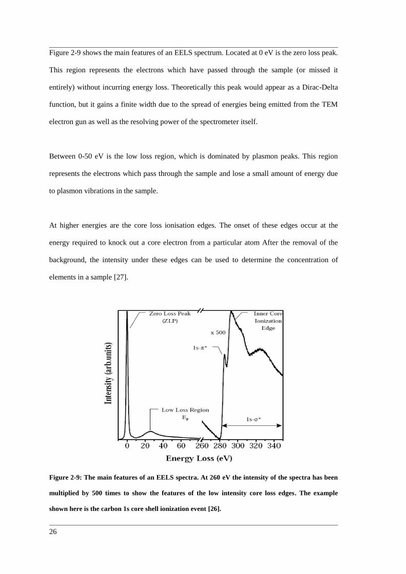
26
Figure 2-9 shows the main features of an EELS spectrum. Located at 0 eV is the zero loss peak.
This region represents the electrons which have passed through the sample (or missed it
entirely) without incurring energy loss. Theoretically this peak would appear as a Dirac-Delta
function, but it gains a finite width due to the spread of energies being emitted from the TEM
electron gun as well as the resolving power of the spectrometer itself.
Between 0-50 eV is the low loss region, which is dominated by plasmon peaks. This region
represents the electrons which pass through the sample and lose a small amount of energy due
to plasmon vibrations in the sample.
At higher energies are the core loss ionisation edges. The onset of these edges occur at the
energy required to knock out a core electron from a particular atom After the removal of the
background, the intensity under these edges can be used to determine the concentration of
elements in a sample [27].
Figure 2-9: The main features of an EELS spectra. At 260 eV the intensity of the spectra has been
multiplied by 500 times to show the features of the low intensity core loss edges. The example
shown here is the carbon 1s core shell ionization event [26].
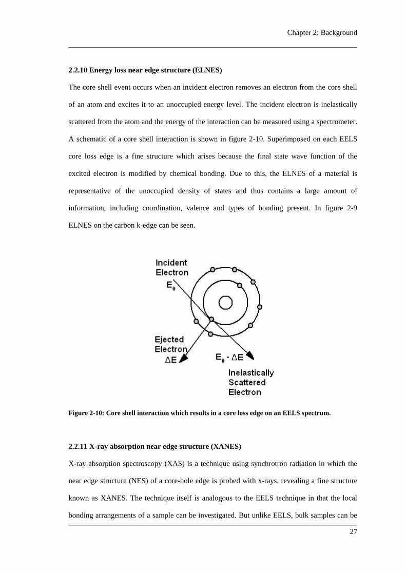
Chapter 2: Background
27
2.2.10 Energy loss near edge structure (ELNES)
The core shell event occurs when an incident electron removes an electron from the core shell
of an atom and excites it to an unoccupied energy level. The incident electron is inelastically
scattered from the atom and the energy of the interaction can be measured using a spectrometer.
A schematic of a core shell interaction is shown in figure 2-10. Superimposed on each EELS
core loss edge is a fine structure which arises because the final state wave function of the
excited electron is modified by chemical bonding. Due to this, the ELNES of a material is
representative of the unoccupied density of states and thus contains a large amount of
information, including coordination, valence and types of bonding present. In figure 2-9
ELNES on the carbon k-edge can be seen.
Figure 2-10: Core shell interaction which results in a core loss edge on an EELS spectrum.
2.2.11 X-ray absorption near edge structure (XANES)
X-ray absorption spectroscopy (XAS) is a technique using synchrotron radiation in which the
near edge structure (NES) of a core-hole edge is probed with x-rays, revealing a fine structure
known as XANES. The technique itself is analogous to the EELS technique in that the local
bonding arrangements of a sample can be investigated. But unlike EELS, bulk samples can be
28
used in the synchrotron, which therefore has the advantage of minimal sample preparation. A
disadvantage of XANES is that there is a relatively poor spatial resolution due to the large x-ray
beam used (typically ~1 mm). However, XANES has a much better energy resolution than can
be achieved in EELS.
In XAS experiments, an x-ray beam is shone onto the sample to excite photoelectrons from the
inner shells (core electrons) from atoms in the sample (figure 2-11a). In order for the electron
to leave the atom, it must be given sufficient energy by the incident x-rays to be promoted to an
unoccupied state above the Fermi energy. Therefore, x-ray absorption spectra, like ELNES,
provides information on the unoccupied DOS of the sample. Several different detectors are
used to measure the intensity as a function of x-ray energy. After the core shell electron (n) is
removed from the atom, a transition will occur where an outer shell electron (n‟) will fill in the
newly created core hole. In dropping down an energy level, the electron releases energy in the
form of a photon (figure 2-11b) or Auger electron (figure 2-11c). Photons are measured using a
fluorescence detector (known as the fluorescence yield, FY) and the Auger electrons are
measured using a hemispherical detector (known as the Auger electron yield, AEY). The other
method for obtaining spectra is by monitoring the total electron yield (TEY, also known as the
drain), in which the back of the sample is connected to ground through an ammeter and the total
number of secondary electrons generated are measured (figure 2-11d).
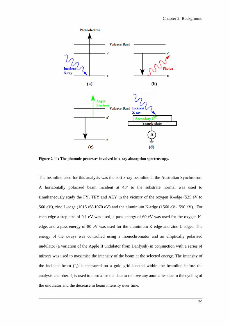
Chapter 2: Background
29
Figure 2-11: The photonic processes involved in x-ray absorption spectroscopy.
The beamline used for this analysis was the soft x-ray beamline at the Australian Synchrotron.
A horizontally polarized beam incident at 45º to the substrate normal was used to
simultaneously study the FY, TEY and AEY in the vicinity of the oxygen K-edge (525 eV to
560 eV), zinc L-edge (1015 eV-1070 eV) and the aluminium K-edge (1560 eV-1590 eV). For
each edge a step size of 0.1 eV was used, a pass energy of 60 eV was used for the oxygen K-
edge, and a pass energy of 80 eV was used for the aluminium K-edge and zinc L-edges. The
energy of the x-rays was controlled using a monochromator and an elliptically polarised
undulator (a variation of the Apple II undulator from Danfysik) in conjunction with a series of
mirrors was used to maximise the intensity of the beam at the selected energy. The intensity of
the incident beam (I0) is measured on a gold grid located within the beamline before the
analysis chamber. I0 is used to normalise the data to remove any anomalies due to the cycling of
the undulator and the decrease in beam intensity over time.
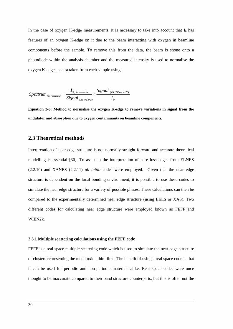
30
In the case of oxygen K-edge measurements, it is necessary to take into account that I0 has
features of an oxygen K-edge on it due to the beam interacting with oxygen in beamline
components before the sample. To remove this from the data, the beam is shone onto a
photodiode within the analysis chamber and the measured intensity is used to normalise the
oxygen K-edge spectra taken from each sample using:
0
),(0
I
Signal
Signal
ISpectrum
TEYorAEYFY
photodiode
photodiode
Normalised
Equation 2-6: Method to normalise the oxygen K-edge to remove variations in signal from the
undulator and absorption due to oxygen contaminants on beamline components.
2.3 Theoretical methods
Interpretation of near edge structure is not normally straight forward and accurate theoretical
modelling is essential [30]. To assist in the interpretation of core loss edges from ELNES
(2.2.10) and XANES (2.2.11) ab initio codes were employed. Given that the near edge
structure is dependent on the local bonding environment, it is possible to use these codes to
simulate the near edge structure for a variety of possible phases. These calculations can then be
compared to the experimentally determined near edge structure (using EELS or XAS). Two
different codes for calculating near edge structure were employed known as FEFF and
WIEN2k.
2.3.1 Multiple scattering calculations using the FEFF code
FEFF is a real space multiple scattering code which is used to simulate the near edge structure
of clusters representing the metal oxide thin films. The benefit of using a real space code is that
it can be used for periodic and non-periodic materials alike. Real space codes were once
thought to be inaccurate compared to their band structure counterparts, but this is often not the
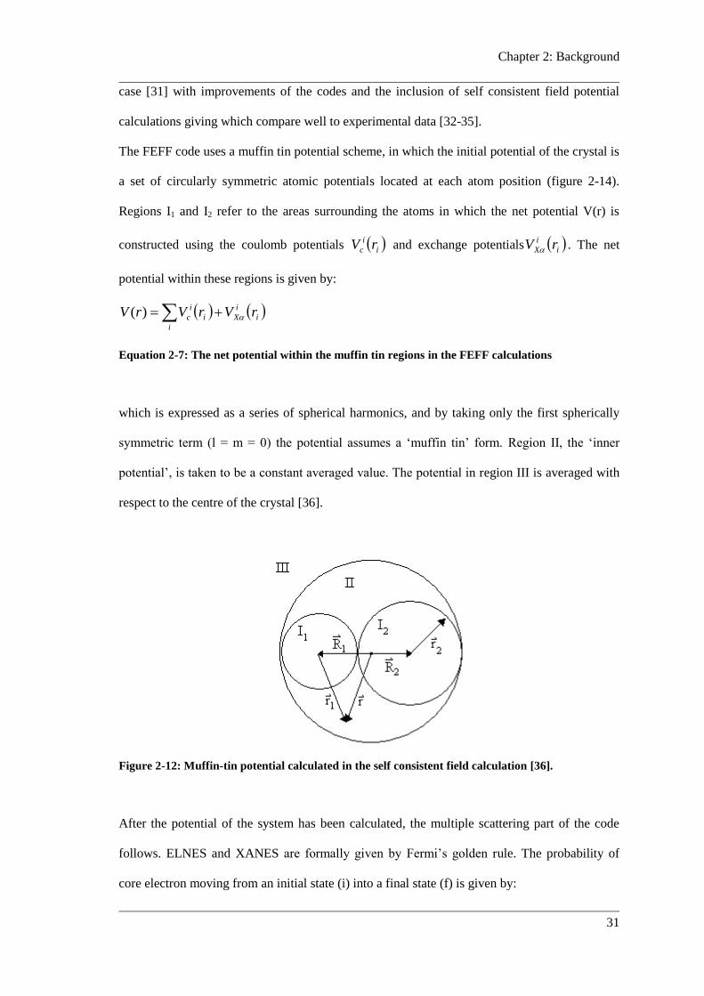
Chapter 2: Background
31
case [31] with improvements of the codes and the inclusion of self consistent field potential
calculations giving which compare well to experimental data [32-35].
The FEFF code uses a muffin tin potential scheme, in which the initial potential of the crystal is
a set of circularly symmetric atomic potentials located at each atom position (figure 2-14).
Regions I1 and I2 refer to the areas surrounding the atoms in which the net potential V(r) is
constructed using the coulomb potentials i
i
c rV and exchange potentials i
i
X rV . The net
potential within these regions is given by:
i
i
Xi
i
i
c rVrVrV )(
Equation 2-7: The net potential within the muffin tin regions in the FEFF calculations
which is expressed as a series of spherical harmonics, and by taking only the first spherically
symmetric term (l = m = 0) the potential assumes a „muffin tin‟ form. Region II, the „inner
potential‟, is taken to be a constant averaged value. The potential in region III is averaged with
respect to the centre of the crystal [36].
Figure 2-12: Muffin-tin potential calculated in the self consistent field calculation [36].
After the potential of the system has been calculated, the multiple scattering part of the code
follows. ELNES and XANES are formally given by Fermi‟s golden rule. The probability of
core electron moving from an initial state (i) into a final state (f) is given by:
32
Ff EE
f
fa EEirfE )(ˆ)(2
Equation 2-8: Fermi's golden rule, describing the probability of core-level electron transition.
where r is the dipole operator for the incident electromagnetic wave interacting with the
material and the sum is over all energies above the Fermi energy (Ef). When the atom absorbs
the incident electron or x-ray and the core hole is formed, the ejected photoelectron propagates
outwardly and scatters from surrounding atoms until the core hole is refilled [33]. Figure 2-13
shows a representation of the photoelectron wavefront scattering from multiple atoms within a
material. Each of these paths must be considered as these multiple scattering events add
towards the final near edge structure on the EELS and XAS core loss edges.
(1)
(2)
(1)
(2)
Figure 2-13: Multiple scattering with the wavefront scattering between multiple atoms in the
material until the core-hole is refilled.
The input structure files for the FEFF code were generated using the atoms code [37]. Into this
program it is possible to insert the space group, the lattice parameters, the electron shell to be
studied, the size of the atomic cluster as well as the crystallographic coordinates of each of the
atoms in the unit cell. The FEFF code often calculated the Fermi energy incorrectly. The
Chapter 2: Background
33
correct Fermi energy was found by examining the DOS and determining the energy of the gap
between occupied and unoccupied states. Calculations were run repeatedly with increasing
number of shells of atoms until increases in cluster size no longer resulted in differences in near
edge structure. Lorentzian broadening to account for experimental and lifetime broadening in
the ELNES and XANES was included in the calculations by adding an imaginary “optical”
potential using the EXCHANGE card [32]. An important consideration when calculating the
NES of a structure is the core-hole effect, which may affect the potentials within the muffin tin
radius. FEFF uses a self consistent fully screened core-hole, which acts in shifting the spectra to
lower energies while increasing the intensity of the main peak [32].
In this thesis, two versions of the FEFF code were used to calculate the near edge spectra.
FEFF8.2 (which will be referred to as FEFF8 for the remainder of this thesis) was used in
chapters 3 and 5. FEFF9, the latest version of the code, was used in chapter 4.
2.3.2 Band structure calculations using the WIEN2k code
Band structure calculations are performed in reciprocal space and are based on density
functional theory in which the electronic structure of many body systems is calculated [38, 39].
From this it is possible to calculate many ground state properties, such as optical constants,
density of states, low loss spectra and high loss spectra. The band structure calculations in this
thesis were performed using the WIEN2k code which uses parameters provided in an input file
to calculate many properties of a crystal. Band structure calculations have the benefit of being
able to calculate many physical properties, however the main drawback for using this technique
is that the properties are calculated for the ground state [40]. Despite this, WIEN2k has been
shown [40-43] to give good results in the simulation of XANES and ELNES spectra. For the
WIEN2k calculations in this thesis, the electron wavefunctions and eigenvalues were calculated
by the full-potential (linearised) augmented plane-wave ((L)APW) + local orbitals (lo) method.
Exchange and correlation were treated using the generalized gradient approximation (GGA).
34
2.4 Bibliography
1. Shi, X., B.K. Tay, H.S. Tan, E. Liu, J. Shi, L.K. Cheah, and X. Jin, Transport of
vacuum arc plasma through an off-plane double bend filtering duct. Thin Solid Films,
1999. 345(1): p. 1-6.
2. Tay, B.K., G.F. You, S.P. Lau, and X. Shi, Plasma flow simulation in an off-plane
double bend magnetic filter. Surface and Coatings Technology, 2000. 133-134: p. 593-
597.
3. Brown, I.G. and X. Godechot, Vacuum arc ion charge-state distributions. Plasma
Science, IEEE Transactions on, 1991. 19(5): p. 713-717.
4. Bilek, M.M.M., The effect of magnetic field configuration on plasma beam profiles in
curved magnetic filters. Journal of Applied Physics, 1999. 85(9): p. 6385-6391.
5. Anders, A., Physics of arcing, and implications to sputter deposition. Thin Solid Films,
2006. 502(1-2): p. 22-28.
6. Aksenov, I.I., V.A. Belous, V.G. Padalka, and V.M. Khoroshikh, Transport of plasma
streams in a curvilinear plasma-optics system. Soviet Journal of Plasma Physics, 1978.
4: p. 425-428.
7. Anders, A., Cathodic Arcs: From Fractal Spots to Energetic Condensation, ed. L.B.N.
Laboratory. 2003: Springer.
8. Xu, S., B.K. Tay, H.S. Tan, L. Zhong, Y.Q. Tu, S.R.P. Silva, and W.I. Milne,
Properties of carbon ion deposited tetrahedral amorphous carbon films as a function of
ion energy. Journal of Applied Physics, 1996. 79(9): p. 7234-7240.
9. Lau, D.W.M., D.G. McCulloch, M.B. Taylor, J.G. Partridge, D.R. McKenzie, N.A.
Marks, E.H.T. Teo, and B.K. Tay, Abrupt Stress Induced Transformation in
Amorphous Carbon Films with a Highly Conductive Transition Phase. Physical
Review Letters, 2008. 100(17): p. 176101.
10. Anders, A., S.H.N. Lim, K.M. Yu, J. Andersson, J. Rosén, M. McFarland, and J.
Brown, High quality ZnO:Al transparent conducting oxide films synthesized by pulsed
filtered cathodic arc deposition. Thin Solid Films, 2010. 518(12): p. 3313-3319.
11. Bräuer, G., B. Szyszka, M. Vergöhl, and R. Bandorf, Magnetron sputtering -
Milestones of 30 years. Vacuum, 2010. 84(12): p. 1354-1359.
12. Chapin, J.S., 'Sputtering process and apparatus', US patent #4,166,018., in Vacuum
Technology. (1974).
13. Kouznetsov, V., K. Macák, J.M. Schneider, U. Helmersson, and I. Petrov, A novel
pulsed magnetron sputter technique utilizing very high target power densities. Surface
and Coatings Technology, 1999. 122(2-3): p. 290-293.
14. Ehiasarian, A.P., R. New, W.D. Münz, L. Hultman, U. Helmersson, and V.
Kouznetsov, Influence of high power densities on the composition of pulsed magnetron
plasmas. Vacuum, 2002. 65(2): p. 147-154.
15. Gudmundsson, J.T., J. Alami, and U. Helmersson, Evolution of the electron energy
distribution and plasma parameters in a pulsed magnetron discharge. Applied Physics
Letters, 2001. 78(22): p. 3427-3429.
16. Lin, J., J.J. Moore, W.D. Sproul, B. Mishra, and Z. Wu, Modulated pulse power
sputtered chromium coatings. Thin Solid Films, 2009. 518(5): p. 1566-1570.
17. VlCek, J., P. KudlaCek, K. Burcalova, and J. Musil, High-power pulsed sputtering
using a magnetron with enhanced plasma confinement. Journal of Vacuum Science &
Technology A: Vacuum, Surfaces, and Films, 2007. 25(1): p. 42-47.
18. Modreanu, M., J. Sancho-Parramon, D. O'Connell, J. Justice, O. Durand, and B. Servet,
Solid phase crystallisation of HfO2 thin films. Materials Science and Engineering B,
2005. 118(1-3): p. 127-131.
19. Gullapalli, S.K., R.S. Vemuri, and C.V. Ramana, Structural transformation induced
changes in the optical properties of nanocrystalline tungsten oxide thin films. Applied
Physics Letters, 2010. 96(17): p. 171903-171903-3.
Chapter 2: Background
35
20. Birks, L.S. and H. Friedman, Particle Size Determination from X-Ray Line Broadening.
Journal of Applied Physics, 1946. 17(8): p. 687-692.
21. Hall, E.H., On a New Action of the Magnet on Electric Currents. American Journal of
Mathematics, 1879. 2(3): p. 287-292.
22. Forsgren, K., A. Harsta, J. Aarik, A. Aidla, J. Westlinder, and J. Olsson, Deposition of
HfO2 Thin Films in HfI4-Based Processes. Journal of The Electrochemical Society,
2002. 149(10): p. F139-F144.
23. Rangarajan, V., H. Bhandari, and T.M. Klein, Comparison of hafnium silicate thin
films on silicon (1 0 0) deposited using thermal and plasma enhanced metal organic
chemical vapor deposition. Thin Solid Films, 2002. 419(1-2): p. 1-4.
24. Moon Sig, J., C. Byung Jin, Y. Chia Ching, D. Siu Hung Chan, W. Sung Jin, S.
Mathew, L. Kanta Bera, N. Balasubramanian, and K. Dim-Lee, Formation of hafnium-
aluminum-oxide gate dielectric using single cocktail liquid source in MOCVD process.
Electron Devices, IEEE Transactions on, 2003. 50(10): p. 2088-2094.
25. Choi, C.H., S.J. Rhee, T.S. Jeon, N. Lu, J.H. Sim, R. Clark, M. Niwa, and D.L. Kwong.
Thermally stable CVD HfOxNy advanced gate dielectrics with poly-Si gate electrode. in
Electron Devices Meeting, 2002. IEDM '02. Digest. International. 2002.
26. Lau, D., Characterisation of Novel Carbonaceous Materials Synthesised Using
Plasmas. 2009, RMIT University: Melbourne.
27. Egerton, R.F., Electron Energy-Loss Spectroscopy in the Electron Microscope. 2 ed.
1996, New York
London: Plenum Press. 227-243.
28. Brydson, R., Electron Energy Loss Spectroscopy. Microscopy Handbooks. 2001: BIOS
Scientific Publishers Limited.
29. Pieranski, P., Colloidal crystals. Contemporary Physics, 1983. 24(1): p. 25 - 73.
30. Keast, V.J., A.J. Scott, R. Brydson, D.B. Williams, and J. Bruley, Electron energy-loss
near-edge structure - a tool for the investigation of electronic structure on the
nanometre scale. Journal of Microscopy, 2001. 203(2): p. 135-175.
31. Rehr, J.J. and R.C. Albers, Theoretical approaches to x-ray absorption fine structure.
Reviews of Modern Physics, 2000. 72(3): p. 621.
32. Moreno, M.S., K. Jorissen, and J.J. Rehr, Practical aspects of electron energy-loss
spectroscopy (EELS) calculations using FEFF8. Micron, 2007. 38(1): p. 1-11.
33. Ravel, B., A practical introduction to multiple scattering theory. Journal of Alloys and
Compounds, 2005. 401(1-2): p. 118-126.
34. Hallmeier, K.H., I. Uhlig, and R. Szargan, Sulphur L2,3 and L1 XANES investigations
of pyrite and marcasite. Journal of Electron Spectroscopy and Related Phenomena,
2002. 122(1): p. 91-96.
35. Ankudinov, A.L., J.J. Rehr, J.J. Low, and S.R. Bare, Theoretical Interpretation of
XAFS and XANES in Pt Clusters. Topics in Catalysis, 2002. 18(1): p. 3-7.
36. Stohr, J., NEXAFS Spectroscopy. Springer Series in Surface Sciences. Vol. 25. 1992.
37. Ravel, B., Webatoms. 2003, http://cars9.uchicago.edu/cgi-bin/atoms/atoms.cgi.
38. Hohenberg, P. and W. Kohn, Inhomogeneous Electron Gas. Physical Review, 1964.
136(3B): p. B864.
39. Kohn, W. and L.J. Sham, Self-Consistent Equations Including Exchange and
Correlation Effects. Physical Review, 1965. 140(4A): p. A1133.
40. Hebert, C., Practical aspects of running the WIEN2k code for electron spectroscopy.
Micron, 2007. 38(1): p. 12-28.
41. Holec, D., P.M.F.J. Costa, P.D. Cherns, and C.J. Humphreys, A theoretical study of
ELNES spectra of AlxGa1-xN using Wien2k and Telnes programs. Computational
Materials Science, 2008. 44(1): p. 91-96.
42. Soldatov, A., G. Yalovega, G. Smolentsev, A. Kravtsova, D. Lamoen, C.
Balasubramanian, A. Marcelli, G. Cinque, and S. Bellucci, ALN nanoparticles XANES
analysis: Local atomic and electronic structure. Nuclear Instruments and Methods in
Physics Research Section A: Accelerators, Spectrometers, Detectors and Associated
Equipment, 2007. 575(1-2): p. 85-87.

36
43. Kunisu, M., F. Oba, H. Ikeno, I. Tanaka, and T. Yamamoto, Local environment of Mn
dopant in ZnO by near-edge x-ray absorption fine structure analysis. Applied Physics
Letters, 2005. 86(12): p. 121902-3.

Chapter 3: The microstructure and electronic structure of tungsten oxide
37
Chapter 3
The microstructure and electronic structure of
tungsten oxide thin films
In this chapter, the microstructure of tungsten oxide (WO3) thin films prepared using pulsed
magnetron sputtering and pulsed cathodic arc deposition is investigated. As discussed in
chapter 2, the differences between these two techniques are significant. Cathodic arc deposited
films are formed from energetic and charged ions while sputtered films are deposited primarily
from low energy neutrals. Transmission electron microscopy (TEM) and electron energy-loss
spectroscopy (EELS) are used to characterize the films. The oxygen K-edge measured with
EELS provides a convenient way of distinguishing between the various phases of WO3. In
addition to experimental measurements, this chapter employs theoretical calculations to
calculate the near edge structure (NES) which is present on each oxygen k-edge for different
phases or WO3. These calculated edges are used to help identify the particular phase of WO3
present in the samples.
38
3.1 Introduction
As discussed in chapter 1, transparent conductive oxides (TCO‟s) are of growing interest to the
scientific community for the purposes of solar cell research and energy saving applications [1].
Electrochromic (EC) coatings have the ability to reversibly change their optical properties by
applying a small on/off voltage. These properties have led to many applications including anti
dazzling rear view mirrors and various display devices [2, 3]. Of specific interest for tungsten
oxide is the production of „smart windows‟ [4]. Using the electrochromic effect it is possible to
manufacture a window with reversible colouration change simply by applying a small voltage.
This is important in energy saving applications, in that large office buildings can be fitted with
these windows and be heated or cooled by controlling the amount of IR radiation allowed into
the building.
3.1.1 Tungsten oxide as a TCO
Of all the transition metal oxide materials studied thus far, WO3 is one of the most extensively
studied [5-7]. In addition to EC applications, WO3 has also been investigated for use in gas
sensing [8], biosensors [9], superconductors [10], imaging recording [11] and optical storage
[12]. Many of these applications require the preparation of high quality thin films. Therefore, it
is important to investigate how different deposition techniques give rise to different film
microstructure. Before considering previous work on tungsten oxide thin films, in the next
section, the type of structures that tungsten oxide forms in the bulk is discussed.
3.1.2 The crystal structure of WO3
Bulk crystalline WO3 is known to have a perovskite type structure which at atmospheric
pressure undergoes several phase changes depending on temperature [13, 14]. However, all of
the tungsten oxide phases are made up of a basic structure comprised of many WO6 octahedral
units. The details of the structure including the W-O distance and the tilting of the octahedral
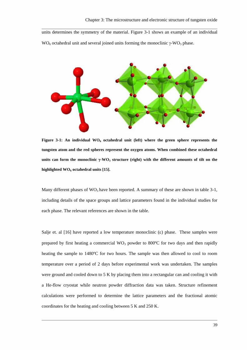
Chapter 3: The microstructure and electronic structure of tungsten oxide
39
units determines the symmetry of the material. Figure 3-1 shows an example of an individual
WO6 octahedral unit and several joined units forming the monoclinic -WO3 phase.
Figure 3-1: An individual WO6 octahedral unit (left) where the green sphere represents the
tungsten atom and the red spheres represent the oxygen atoms. When combined these octahedral
units can form the monoclinic -WO3 structure (right) with the different amounts of tilt on the
highlighted WO6 octahedral units [15].
Many different phases of WO3 have been reported. A summary of these are shown in table 3-1,
including details of the space groups and lattice parameters found in the individual studies for
each phase. The relevant references are shown in the table.
Salje et. al [16] have reported a low temperature monoclinic () phase. These samples were
prepared by first heating a commercial WO3 powder to 800ºC for two days and then rapidly
heating the sample to 1480ºC for two hours. The sample was then allowed to cool to room
temperature over a period of 2 days before experimental work was undertaken. The samples
were ground and cooled down to 5 K by placing them into a rectangular can and cooling it with
a He-flow cryostat while neutron powder diffraction data was taken. Structure refinement
calculations were performed to determine the lattice parameters and the fractional atomic
coordinates for the heating and cooling between 5 K and 250 K.
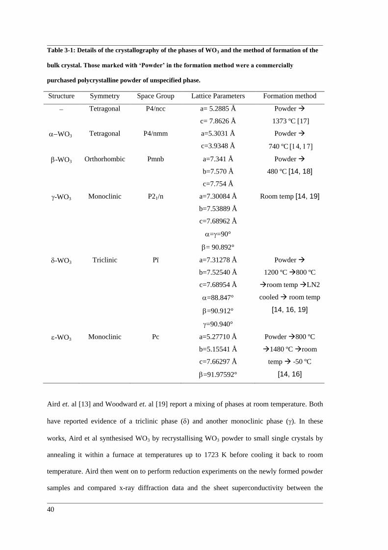
40
Table 3-1: Details of the crystallography of the phases of WO3 and the method of formation of the
bulk crystal. Those marked with ‘Powder’ in the formation method were a commercially
purchased polycrystalline powder of unspecified phase.
Structure Symmetry Space Group Lattice Parameters Formation method
Tetragonal P4/ncc a= 5.2885 Å
c= 7.8626 Å
Powder
1373 ºC [17]
WO3 Tetragonal P4/nmm a=5.3031 Å
c=3.9348 Å
Powder
740 ºC
-WO3 Orthorhombic Pmnb a=7.341 Å
b=7.570 Å
c=7.754 Å
Powder
480 ºC [14, 18]
-WO3 Monoclinic P21/n a=7.30084 Å
b=7.53889 Å
c=7.68962 Å
==90°
= 90.892°
Room temp [14, 19]
-WO3 Triclinic Pī a=7.31278 Å
b=7.52540 Å
c=7.68954 Å
=88.847°
=90.912°
=90.940°
Powder
1200 ºC 800 ºC
room temp LN2
cooled room temp
[14, 16, 19]
-WO3 Monoclinic Pc a=5.27710 Å
b=5.15541 Å
c=7.66297 Å
=91.97592°
Powder 800 ºC
1480 ºC room
temp -50 ºC
[14, 16]
Aird et. al [13] and Woodward et. al [19] report a mixing of phases at room temperature. Both
have reported evidence of a triclinic phase () and another monoclinic phase (). In these
works, Aird et al synthesised WO3 by recrystallising WO3 powder to small single crystals by
annealing it within a furnace at temperatures up to 1723 K before cooling it back to room
temperature. Aird then went on to perform reduction experiments on the newly formed powder
samples and compared x-ray diffraction data and the sheet superconductivity between the
Chapter 3: The microstructure and electronic structure of tungsten oxide
41
reduced sample and the fully stoichiometric WO3. In the study performed by Woodward et al
[19], neutron powder diffraction was performed on WO3 samples that had first been heated to
1200ºC in air, and then cooled in stages to room temperature. It was found that the samples
contained mixed phases of both triclinic () and monoclinic phases (). The sample was then
cooled in liquid nitrogen and then allowed to heat back up to room temperature. Repeating the
same neutron diffraction experiment yielded only single phase triclinic WO3. Using this neutron
data, Rietveld structure refinement calculations were performed to determine the lattice
parameters and the oxygen/tungsten positional parameters of the triclinic structure.
At elevated temperatures of 480ºC and 770ºC -WO3 transforms into orthorhombic () and then
to tetragonal () phases respectively. The -WO3 was studied by Salje et al [18] in which -
WO3 crystals were placed onto nickel wire and heat treated to form orthorhombic crystals of
space group Pnmb. The lattice parameters a,b and c as well as the atomic positions of the 2
unique tungsten atoms and 8 unique oxygen atoms were determined using x-ray analysis.
The -WO3 phase was studied and refined by Locherer in 1999 [17] using ab initio
calculations. In this work the superconductive nature of WO3 was studied, as well as the
existence of further tetragonal phases when the sample is heated beyond 1100 K. At this high
temperature, a new tetragonal phase (shown in table 3-1 with space group P4/ncc) was found
with slightly different lattice parameters, as well as slight shifting in the WO6 octahedra about
the [001] direction.
3.1.3 Growth of thin films of WO3
WO3 films have been deposited using several methods including sputtering [5, 6], evaporation
[20, 21], pulsed laser deposition [22] and filtered cathodic arc deposition [23]. In general, the
microstructure and performance of the films depends on the method, deposition temperature
and other process conditions, with both amorphous and polycrystalline materials reported [24].
42
In the work by Cui et al [5], a dc magnetron sputterer was used to deposit the WO3 films grown
specifically for the purpose of smart windows. It was found that the films were initially
amorphous, however the microstructure changed and monoclinic crystals formed following
annealing to 500ºC. Given the importance of this research for smart windows, it would have
been very important for this study to perform electron microscopy and diffraction on the films
to get a stronger understanding of the microstructure being deposited. It has been accepted that
highly disordered films perform better as EC devices [25], so it would also have been
interesting for the authors to have published transmittance and electrical measurements on the
500ºC film to see how great a change in these properties a crystalline film has over an
amorphous film.
Gillet et al [20] and Shigesato et al [21] used a simple thermal evaporator for deposition. Gillet
deposited the WO3 films onto an alumina substrate and found that the as-deposited films were
highly disordered and showed broad rings in the reflection high energy electron diffraction
(RHEED) patterns. Annealing these films resulted in the crystals aligning and an observable
single crystal diffraction which was indexed to a <001> oriented monoclinic structure. TEM
and electron diffraction data is presented in this paper clearly showing the difference in
microstructures between the two films. Shigesato used Raman Spectroscopy to study WO3
films evaporated onto glass substrates. It was found that the as-deposited films were
amorphous, but crystallinity of the films increased when annealed between 40ºC and 145ºC.
Although both of these thermal evaporation studies of WO3 look at many aspects of the films,
neither of them probe the electronic structure of the films. This could have been performed
easily with x-ray photoelectron spectroscopy (XPS), EELS or x-ray absorption spectroscopy
(XAS). This not only would have allowed for confirmation that the deposited films were
stoichiometric, but it would have given in depth knowledge on the bonding configurations
between the tungsten and oxygen atoms.
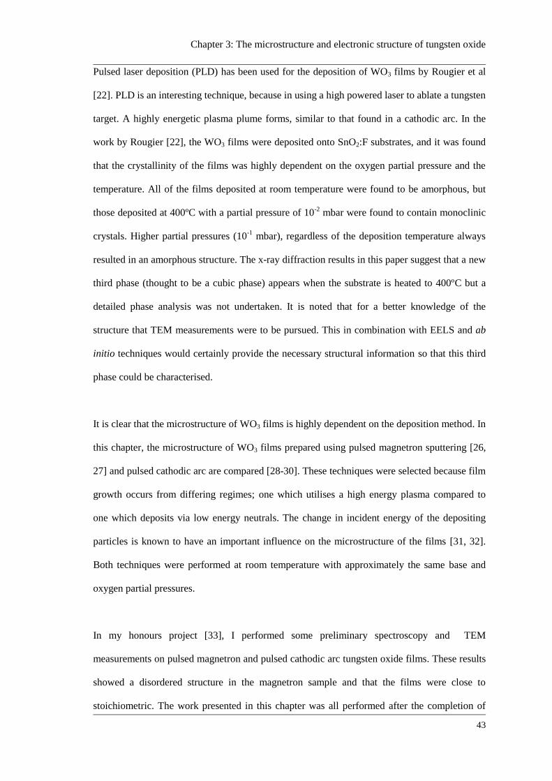
Chapter 3: The microstructure and electronic structure of tungsten oxide
43
Pulsed laser deposition (PLD) has been used for the deposition of WO3 films by Rougier et al
[22]. PLD is an interesting technique, because in using a high powered laser to ablate a tungsten
target. A highly energetic plasma plume forms, similar to that found in a cathodic arc. In the
work by Rougier [22], the WO3 films were deposited onto SnO2:F substrates, and it was found
that the crystallinity of the films was highly dependent on the oxygen partial pressure and the
temperature. All of the films deposited at room temperature were found to be amorphous, but
those deposited at 400ºC with a partial pressure of 10-2
mbar were found to contain monoclinic
crystals. Higher partial pressures (10-1
mbar), regardless of the deposition temperature always
resulted in an amorphous structure. The x-ray diffraction results in this paper suggest that a new
third phase (thought to be a cubic phase) appears when the substrate is heated to 400ºC but a
detailed phase analysis was not undertaken. It is noted that for a better knowledge of the
structure that TEM measurements were to be pursued. This in combination with EELS and ab
initio techniques would certainly provide the necessary structural information so that this third
phase could be characterised.
It is clear that the microstructure of WO3 films is highly dependent on the deposition method. In
this chapter, the microstructure of WO3 films prepared using pulsed magnetron sputtering [26,
27] and pulsed cathodic arc are compared [28-30]. These techniques were selected because film
growth occurs from differing regimes; one which utilises a high energy plasma compared to
one which deposits via low energy neutrals. The change in incident energy of the depositing
particles is known to have an important influence on the microstructure of the films [31, 32].
Both techniques were performed at room temperature with approximately the same base and
oxygen partial pressures.
In my honours project [33], I performed some preliminary spectroscopy and TEM
measurements on pulsed magnetron and pulsed cathodic arc tungsten oxide films. These results
showed a disordered structure in the magnetron sample and that the films were close to
stoichiometric. The work presented in this chapter was all performed after the completion of
44
my honours project and includes much more detailed measurements including high resolution
TEM imaging, diffraction patterns as well as the use of the ab initio calculations to help
interpret the NES observed on the absorption edges measured using EELS.
3.2 Experimental Techniques
3.2.1 Deposition using pulsed cathodic arc
Details of the cathodic arc deposition system are provided in chapter 2, For the WO3
depositions, the chamber was pumped down to a base pressure of about 7 x 10⁻⁶
Torr (9 x 10⁻⁴
Pa) and backfilled with O2 at a flow rate of 10 sccm to a pressure of about 6.6 mTorr (0.88 Pa).
The pulsed arc source [34], equipped with a tungsten rod cathode and a 90° open-coil
macroparticle filter, was fed from a switched capacitor bank (0.3 F) charged to 270 V, resulting
in an arc current of about 180 A, limited by a 1.5 Ω resistor in series. The arc repetition rate
was 3 pulses per second each with a duration of 3 ms. After 7600 pulses, a film thickness of
200 nm was obtained, with the holder placed about 90 mm from the filter exit. Throughout the
deposition process, the sample holder was pulsed-biased to -200 V with pulse cycle of 10 s on
(-200 V) and 90 s off (ground).
3.2.2 Deposition using magnetron sputtering
The magnetron sputtering was performed in the system outlined in chapter 2. The chamber was
initially pumped down to a base pressure of about 1.3x10⁻⁶
Torr (1.7 x 10⁻⁴
Pa) using a
cryogenic pump with a pumping speed of 1500 l/s. The pumping speed was reduced using an
adjustable gate valve to obtain a relatively high total pressure of 42 mTorr (5.6 Pa) with Ar and
O2 gas flows of 50 and 40 sccm, respectively. The gas was introduced into a gas plasma source
of the constricted plasma source type [35] operated with a Pinnacle Plus power supply at 1500
W (pulsed-DC, 100 kHz, 1 s reverse time). It was noted that the total pressure was reduced to
about 36 mTorr (4.8 Pa) during deposition, which is due to the consumption of oxygen by the
Chapter 3: The microstructure and electronic structure of tungsten oxide
45
growing film. A 76 mm diameter W target with a sputter power of 1200 W was used. The
substrate was placed 90 mm away from the sputtering gun and the plasma source. Total
deposition time was 10 mins.
3.2.2 Theoretical methods
Using the structures outlined in table 3-1, ab initio simulations were performed to calculate the
oxygen K-edge using both multiple scattering and band structure calculations.
The multiple scattering calculations were performed using the FEFF8 code (outlined in section
2.6). Cluster sizes of up to approximately 150 atoms as found to be sufficient to obtain
convergence. A core-hole following the final state rule was used because it was found to
provide a better approximation of the NES. A muffin-tin overlap of 15% was employed and the
Hedin–Lundqvist exchange potential was used as it is recommended for solids [36]. Each of the
WO3 structures listed in table 3-1 has multiple unique oxygen positions in the unit cell.
Therefore, the NES of each unique oxygen atom was modelled separately and then combined to
provide an average. Unbroadened spectra were used to compare the features on the calculated
WO3 phases. Lorentzian broadening of 1.3 eV was included into the calculation by adding the
imaginary optical potential (as detailed in section 2.3.1) in order to compare with the
experimental ELNES and XANES spectra.
For the WIEN2k calculations, the parameter determining the size of the basis set, RMTKMAX,
was set to 7. The muffin tin radii were chosen as large as possible but without overlapping
spheres. The number of k-points in the irreducible Brillouin zone (BZ) was 90 for -WO3 and
54 for -WO3. Convergence tests showed that this number of k-points were adequate. A core-
hole was not included in the results presented here, as it only changed the relative intensity of
peaks by a small amount, but with a considerable increase in computational time. The oxygen
K-edge was calculated using the XSPEC subroutine within WIEN2k. Spectra were calculated
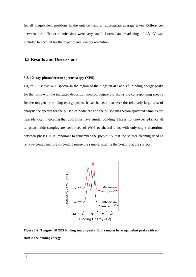
46
for all inequivalent positions in the unit cell and an appropriate average taken. Differences
between the different atomic sites were very small. Lorentzian broadening of 1.3 eV was
included to account for the experimental energy resolution.
3.3 Results and Discussions
3.3.1 X-ray photoelectron spectroscopy (XPS)
Figure 3-2 shows XPS spectra in the region of the tungsten 4f7 and 4f5 binding energy peaks
for the films with the indicated deposition method. Figure 3-3 shows the corresponding spectra
for the oxygen 1s binding energy peaks. It can be seen that over the relatively large area of
analysis the spectra for the pulsed cathodic arc and the pulsed magnetron sputtered samples are
near identical, indicating that both films have similar bonding. This is not unexpected since all
tungsten oxide samples are comprised of WO6 octahedral units with only slight distortions
between phases. It is important to remember the possibility that the sputter cleaning used to
remove contaminants also could damage the sample, altering the bonding at the surface.
44 40 36 32 28
Inte
nsity (
arb
. u
nits)
Binding Energy (eV)
Cathodic Arc
Magnetron
Figure 3-2: Tungsten 4f XPS binding energy peaks. Both samples have equivalent peaks with no
shift in the binding energy.
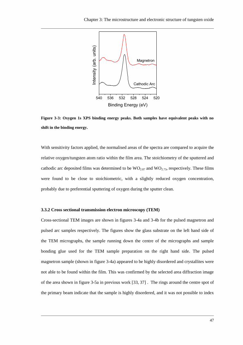
Chapter 3: The microstructure and electronic structure of tungsten oxide
47
540 536 532 528 524 520 I
nte
nsity (
arb
. u
nits)
Binding Energy (eV)
Magnetron
Cathodic Arc
Figure 3-3: Oxygen 1s XPS binding energy peaks. Both samples have equivalent peaks with no
shift in the binding energy.
With sensitivity factors applied, the normalised areas of the spectra are compared to acquire the
relative oxygen/tungsten atom ratio within the film area. The stoichiometry of the sputtered and
cathodic arc deposited films was determined to be WO2.87 and WO2.73, respectively. These films
were found to be close to stoichiometric, with a slightly reduced oxygen concentration,
probably due to preferential sputtering of oxygen during the sputter clean.
3.3.2 Cross sectional transmission electron microscopy (TEM)
Cross-sectional TEM images are shown in figures 3-4a and 3-4b for the pulsed magnetron and
pulsed arc samples respectively. The figures show the glass substrate on the left hand side of
the TEM micrographs, the sample running down the centre of the micrographs and sample
bonding glue used for the TEM sample preparation on the right hand side. The pulsed
magnetron sample (shown in figure 3-4a) appeared to be highly disordered and crystallites were
not able to be found within the film. This was confirmed by the selected area diffraction image
of the area shown in figure 3-5a in previous work [33, 37] . The rings around the centre spot of
the primary beam indicate that the sample is highly disordered, and it was not possible to index
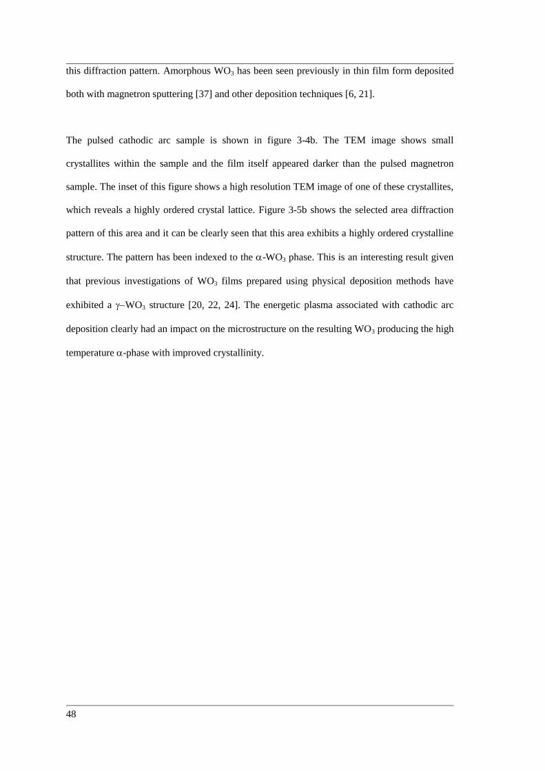
48
this diffraction pattern. Amorphous WO3 has been seen previously in thin film form deposited
both with magnetron sputtering [37] and other deposition techniques [6, 21].
The pulsed cathodic arc sample is shown in figure 3-4b. The TEM image shows small
crystallites within the sample and the film itself appeared darker than the pulsed magnetron
sample. The inset of this figure shows a high resolution TEM image of one of these crystallites,
which reveals a highly ordered crystal lattice. Figure 3-5b shows the selected area diffraction
pattern of this area and it can be clearly seen that this area exhibits a highly ordered crystalline
structure. The pattern has been indexed to the -WO3 phase. This is an interesting result given
that previous investigations of WO3 films prepared using physical deposition methods have
exhibited a WO3 structure [20, 22, 24]. The energetic plasma associated with cathodic arc
deposition clearly had an impact on the microstructure on the resulting WO3 producing the high
temperature -phase with improved crystallinity.

Chapter 3: The microstructure and electronic structure of tungsten oxide
49
Figure 3-4: Cross-sectional TEM Images of the deposited films. (a) Magnetron sputtered sample
(b) Cathodic arc sample. Insert: high resolution image of cathodic arc sample.
50
Figure 3-5: Selected area diffraction patterns of the (a) magnetron sputtered [33] and (b) cathodic
arc films shown in figure 3-4. The diffraction pattern in (b) has been indexed to -WO3.
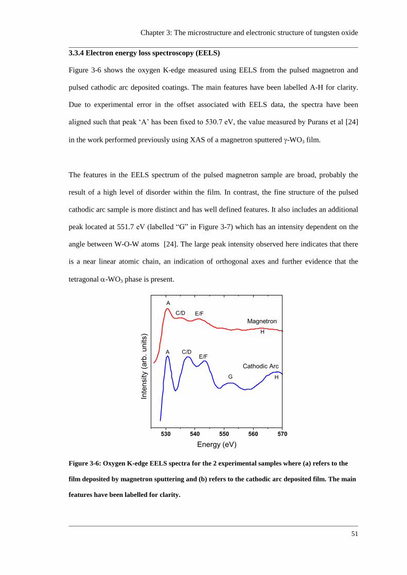
Chapter 3: The microstructure and electronic structure of tungsten oxide
51
3.3.4 Electron energy loss spectroscopy (EELS)
Figure 3-6 shows the oxygen K-edge measured using EELS from the pulsed magnetron and
pulsed cathodic arc deposited coatings. The main features have been labelled A-H for clarity.
Due to experimental error in the offset associated with EELS data, the spectra have been
aligned such that peak „A‟ has been fixed to 530.7 eV, the value measured by Purans et al [24]
in the work performed previously using XAS of a magnetron sputtered -WO3 film.
The features in the EELS spectrum of the pulsed magnetron sample are broad, probably the
result of a high level of disorder within the film. In contrast, the fine structure of the pulsed
cathodic arc sample is more distinct and has well defined features. It also includes an additional
peak located at 551.7 eV (labelled “G” in Figure 3-7) which has an intensity dependent on the
angle between W-O-W atoms [24]. The large peak intensity observed here indicates that there
is a near linear atomic chain, an indication of orthogonal axes and further evidence that the
tetragonal -WO3 phase is present.
530 540 550 560 570
H
E/FC/DA
Inte
nsity (
arb
. u
nits)
Energy (eV)
A
C/D E/F
G H
Magnetron
Cathodic Arc
Figure 3-6: Oxygen K-edge EELS spectra for the 2 experimental samples where (a) refers to the
film deposited by magnetron sputtering and (b) refers to the cathodic arc deposited film. The main
features have been labelled for clarity.
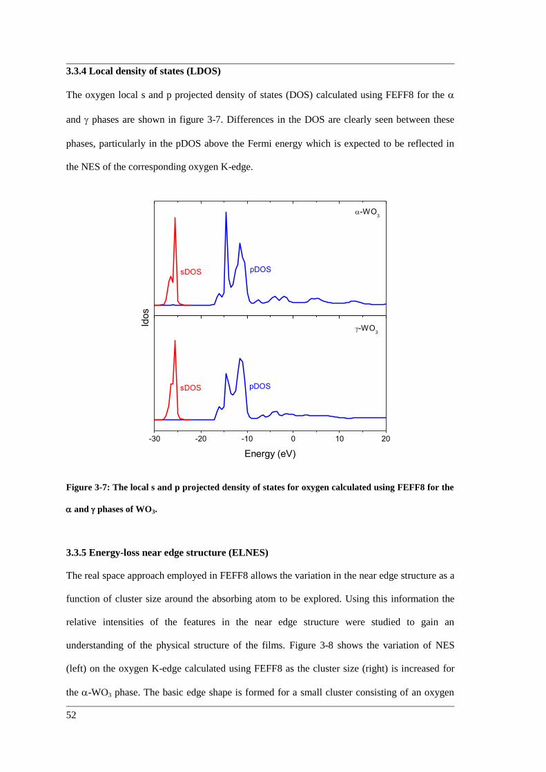
52
3.3.4 Local density of states (LDOS)
The oxygen local s and p projected density of states (DOS) calculated using FEFF8 for the
and phases are shown in figure 3-7. Differences in the DOS are clearly seen between these
phases, particularly in the pDOS above the Fermi energy which is expected to be reflected in
the NES of the corresponding oxygen K-edge.
sDOS
sDOS pDOS
pDOS
-WO3
-WO3
ldo
s
-30 -20 -10 0 10 20
Energy (eV)
Figure 3-7: The local s and p projected density of states for oxygen calculated using FEFF8 for the
and phases of WO3.
3.3.5 Energy-loss near edge structure (ELNES)
The real space approach employed in FEFF8 allows the variation in the near edge structure as a
function of cluster size around the absorbing atom to be explored. Using this information the
relative intensities of the features in the near edge structure were studied to gain an
understanding of the physical structure of the films. Figure 3-8 shows the variation of NES
(left) on the oxygen K-edge calculated using FEFF8 as the cluster size (right) is increased for
the -WO3 phase. The basic edge shape is formed for a small cluster consisting of an oxygen
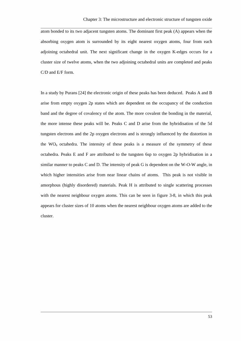
Chapter 3: The microstructure and electronic structure of tungsten oxide
53
atom bonded to its two adjacent tungsten atoms. The dominant first peak (A) appears when the
absorbing oxygen atom is surrounded by its eight nearest oxygen atoms, four from each
adjoining octahedral unit. The next significant change in the oxygen K-edges occurs for a
cluster size of twelve atoms, when the two adjoining octahedral units are completed and peaks
C/D and E/F form.
In a study by Purans [24] the electronic origin of these peaks has been deduced. Peaks A and B
arise from empty oxygen 2p states which are dependent on the occupancy of the conduction
band and the degree of covalency of the atom. The more covalent the bonding in the material,
the more intense these peaks will be. Peaks C and D arise from the hybridisation of the 5d
tungsten electrons and the 2p oxygen electrons and is strongly influenced by the distortion in
the WO6 octahedra. The intensity of these peaks is a measure of the symmetry of these
octahedra. Peaks E and F are attributed to the tungsten 6sp to oxygen 2p hybridisation in a
similar manner to peaks C and D. The intensity of peak G is dependent on the W-O-W angle, in
which higher intensities arise from near linear chains of atoms. This peak is not visible in
amorphous (highly disordered) materials. Peak H is attributed to single scattering processes
with the nearest neighbour oxygen atoms. This can be seen in figure 3-8, in which this peak
appears for cluster sizes of 10 atoms when the nearest neighbour oxygen atoms are added to the
cluster.
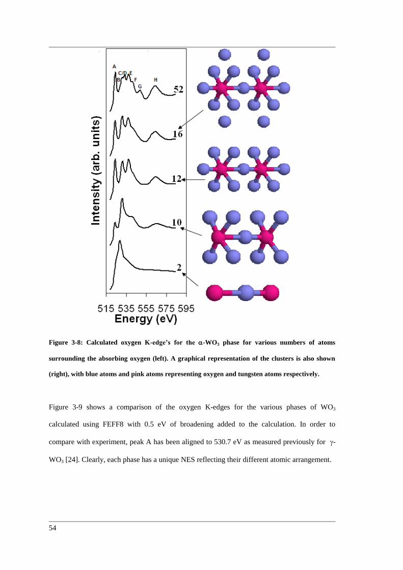
54
Figure 3-8: Calculated oxygen K-edge’s for the -WO3 phase for various numbers of atoms
surrounding the absorbing oxygen (left). A graphical representation of the clusters is also shown
(right), with blue atoms and pink atoms representing oxygen and tungsten atoms respectively.
Figure 3-9 shows a comparison of the oxygen K-edges for the various phases of WO3
calculated using FEFF8 with 0.5 eV of broadening added to the calculation. In order to
compare with experiment, peak A has been aligned to 530.7 eV as measured previously for -
WO3 [24]. Clearly, each phase has a unique NES reflecting their different atomic arrangement.
Chapter 3: The microstructure and electronic structure of tungsten oxide
55
Figure 3-9: The calculated oxygen K-edge NES for the known phases of WO3. The main features
have been labelled and their energies have been listed in table 3-2.
Calculations of the oxygen K-edges were also performed using the WIEN2k code [38] on the
tetragonal -WO3 phase and the monoclinic -WO3 phase. Figure 3-10 compares the oxygen K-
edge of -WO3 calculated using FEFF8 and that obtained using WIEN2k. Also shown is the
oxygen K-edge obtained using XAS for a sputtered WO3 film which was identified as being -
WO3 [24]. Overall, the results are similar with the main features reproduced using both
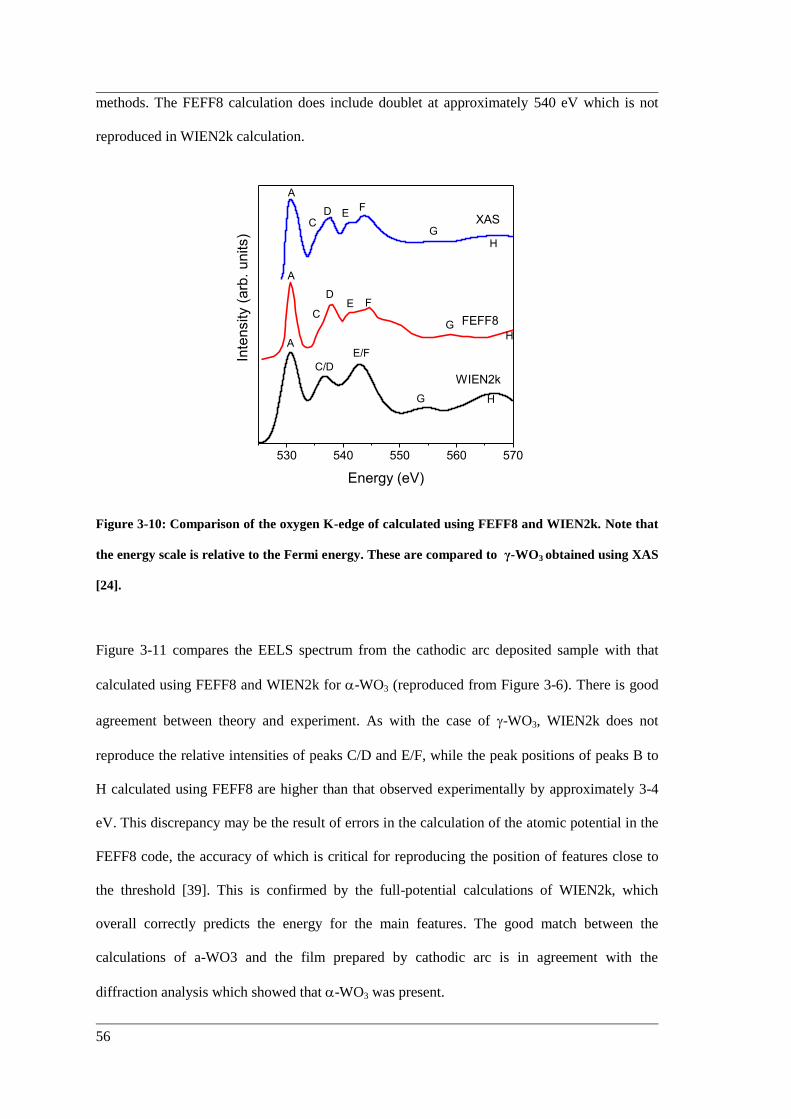
56
methods. The FEFF8 calculation does include doublet at approximately 540 eV which is not
reproduced in WIEN2k calculation.
530 540 550 560 570
F
C
H
E
E/F
C/D
G
AH
G
D
C
A
HG
FE
A
D
WIEN2k
FEFF8
XAS
Inte
nsity (
arb
. units)
Energy (eV)
Figure 3-10: Comparison of the oxygen K-edge of calculated using FEFF8 and WIEN2k. Note that
the energy scale is relative to the Fermi energy. These are compared to γ-WO3 obtained using XAS
[24].
Figure 3-11 compares the EELS spectrum from the cathodic arc deposited sample with that
calculated using FEFF8 and WIEN2k for -WO3 (reproduced from Figure 3-6). There is good
agreement between theory and experiment. As with the case of -WO3, WIEN2k does not
reproduce the relative intensities of peaks C/D and E/F, while the peak positions of peaks B to
H calculated using FEFF8 are higher than that observed experimentally by approximately 3-4
eV. This discrepancy may be the result of errors in the calculation of the atomic potential in the
FEFF8 code, the accuracy of which is critical for reproducing the position of features close to
the threshold [39]. This is confirmed by the full-potential calculations of WIEN2k, which
overall correctly predicts the energy for the main features. The good match between the
calculations of a-WO3 and the film prepared by cathodic arc is in agreement with the
diffraction analysis which showed that -WO3 was present.
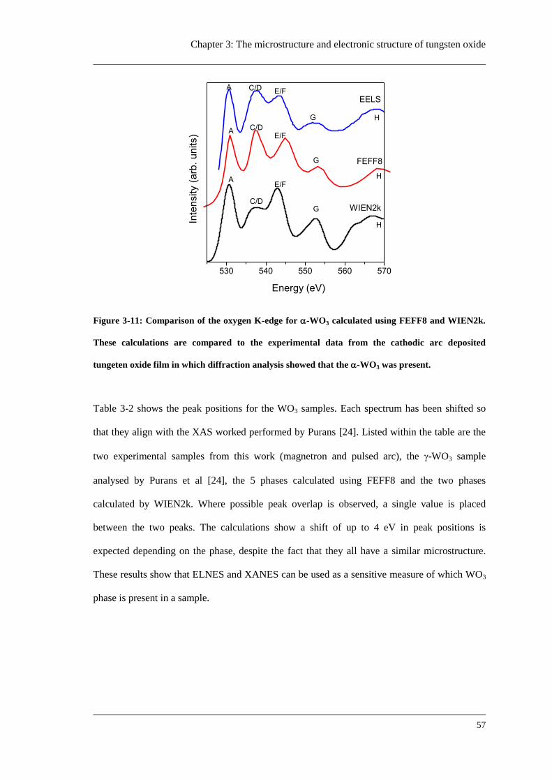
Chapter 3: The microstructure and electronic structure of tungsten oxide
57
530 540 550 560 570
H
WIEN2k
FEFF8
Inte
nsity (
arb
. units)
Energy (eV)
EELS
G
E/FA
C/D
HG
E/FC/DA
H
G
E/FC/DA
Figure 3-11: Comparison of the oxygen K-edge for -WO3 calculated using FEFF8 and WIEN2k.
These calculations are compared to the experimental data from the cathodic arc deposited
tungeten oxide film in which diffraction analysis showed that the -WO3 was present.
Table 3-2 shows the peak positions for the WO3 samples. Each spectrum has been shifted so
that they align with the XAS worked performed by Purans [24]. Listed within the table are the
two experimental samples from this work (magnetron and pulsed arc), the -WO3 sample
analysed by Purans et al [24], the 5 phases calculated using FEFF8 and the two phases
calculated by WIEN2k. Where possible peak overlap is observed, a single value is placed
between the two peaks. The calculations show a shift of up to 4 eV in peak positions is
expected depending on the phase, despite the fact that they all have a similar microstructure.
These results show that ELNES and XANES can be used as a sensitive measure of which WO3
phase is present in a sample.
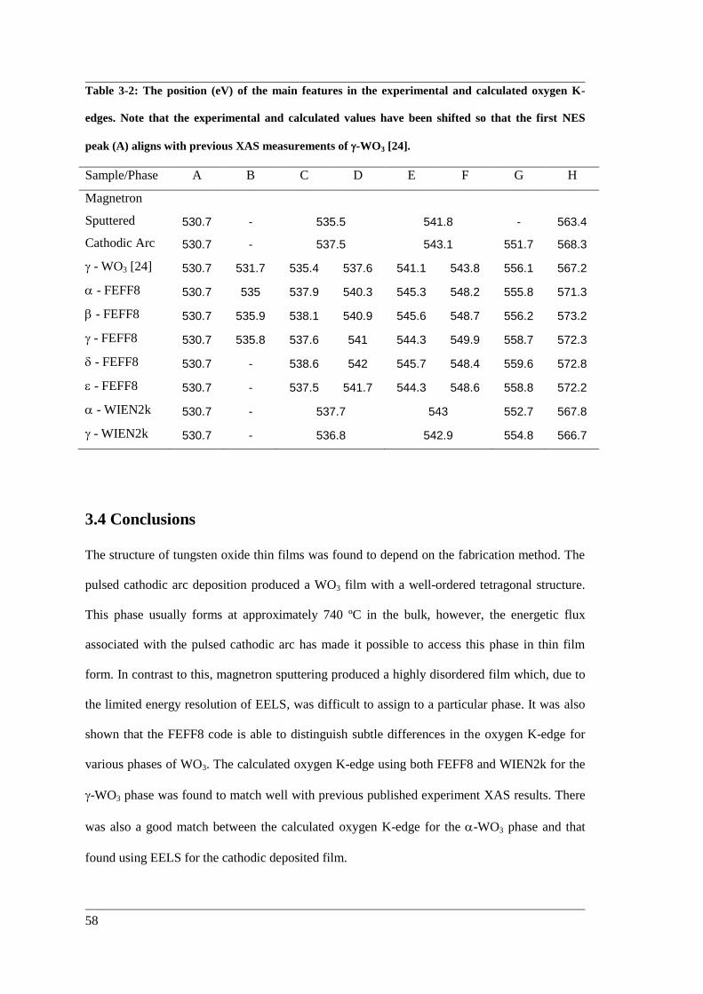
58
Table 3-2: The position (eV) of the main features in the experimental and calculated oxygen K-
edges. Note that the experimental and calculated values have been shifted so that the first NES
peak (A) aligns with previous XAS measurements of -WO3 [24].
Sample/Phase A B C D E F G H
Magnetron
Sputtered 530.7 - 535.5 541.8 - 563.4
Cathodic Arc 530.7 - 537.5 543.1 551.7 568.3
- WO3 [24] 530.7 531.7 535.4 537.6 541.1 543.8 556.1 567.2
- FEFF8 530.7 535 537.9 540.3 545.3 548.2 555.8 571.3
- FEFF8 530.7 535.9 538.1 540.9 545.6 548.7 556.2 573.2
- FEFF8 530.7 535.8 537.6 541 544.3 549.9 558.7 572.3
- FEFF8 530.7 - 538.6 542 545.7 548.4 559.6 572.8
- FEFF8 530.7 - 537.5 541.7 544.3 548.6 558.8 572.2
- WIEN2k 530.7 - 537.7 543 552.7 567.8
- WIEN2k 530.7 - 536.8 542.9 554.8 566.7
3.4 Conclusions
The structure of tungsten oxide thin films was found to depend on the fabrication method. The
pulsed cathodic arc deposition produced a WO3 film with a well-ordered tetragonal structure.
This phase usually forms at approximately 740 ºC in the bulk, however, the energetic flux
associated with the pulsed cathodic arc has made it possible to access this phase in thin film
form. In contrast to this, magnetron sputtering produced a highly disordered film which, due to
the limited energy resolution of EELS, was difficult to assign to a particular phase. It was also
shown that the FEFF8 code is able to distinguish subtle differences in the oxygen K-edge for
various phases of WO3. The calculated oxygen K-edge using both FEFF8 and WIEN2k for the
-WO3 phase was found to match well with previous published experiment XAS results. There
was also a good match between the calculated oxygen K-edge for the -WO3 phase and that
found using EELS for the cathodic deposited film.
Chapter 3: The microstructure and electronic structure of tungsten oxide
59
3.5 Bibliography
1. Azens and Granqvist, Electrochromic smart windows: energy efficiency and device
aspects. Journal of Solid State Electrochemistry, 2003. 7(2): p. 64-68.
2. Su, L., J. Fang, Z. Xiao, and Z. Lu, An all-solid-state electrochromic display device of
prussian blue and WO3 particulate film with a PMMA gel electrolyte. Thin Solid
Films, 1997. 306(1): p. 133-136.
3. Delichère, P., P. Falaras, and A. Hugot-Le Goff, WO3 anodic films in organic medium
for electrochromic display devices. Solar Energy Materials, 1989. 19(3-5): p. 323-333.
4. Cui, H.N., M.F. Costa, V. Teixeira, I. Porqueras, and E. Bertran, Electrochromic
coatings for smart windows. Surface Science
Proceedings of the 7th International Conference on Nanometer-Scale Science and
Technology and the 21st European Conference on Surface Science, 2003. 532-535: p.
1127-1131.
5. Cui, H.N., M.F. Costa, V. Teixeira, I. Porqueras, and E. Bertran, Electrochromic
coatings for smart windows. Surface Science Proceedings of the 7th International
Conference on Nanometer-Scale Science and Technology and the 21st European
Conference on Surface Science, 2003. 532-535: p. 1127-1131.
6. Akl, A.A., H. Kamal, and K. Abdel-Hady, Characterization of tungsten oxide films of
different crystallinity prepared by RF sputtering. Physica B: Condensed Matter, 2003.
325: p. 65-75.
7. Granquist, C.G., Handbook of Inorganic Electrochromic Materials. 1995, Amsterdam:
Elsevier.
8. Labidi, A., C. Jacolin, M. Bendahan, A. Abdelghani, J. Guérin, K. Aguir, and M.
Maaref, Impedance spectroscopy on WO3 gas sensor. Sensors and Actuators B:
Chemical, 2005. 106(2): p. 713-718.
9. Deng, Z., Y. Gong, Y. Luo, and Y. Tian, WO3 nanostructures facilitate electron
transfer of enzyme: Application to detection of H2O2 with high selectivity. Biosensors
and Bioelectronics, 2009. 24(8): p. 2465-2469.
10. Yong, F., Z. Lian, D. Shejun, W. Jinrong, Z. Pingxiang, S. Lei, and Z. Yuheng,
Superconductivity in quenched YBCO---WO3 system. Physica C: Superconductivity,
1994. 235-240(Part 1): p. 405-406.
11. Yuan, H., D.E. Laughlin, X. Zhu, and B. Lu, Ru + oxide interlayer for perpendicular
magnetic recording media. Journal of Applied Physics, 2008. 103(7): p. 07F513.
12. Bussjager, R., J.M. Osman, E. Voss, and J. Chaiken. Tungsten oxide based media for
optical data storage and switching applications. in Aerospace Conference, 1999.
Proceedings. 1999 IEEE. 1999.
13. Aird, A., M.C. Domeneghetti, F. Mazzi, V. Tazzoli, and E.K.H. Salje, Sheet
superconductivity in : crystal structure of the tetragonal matrix. Journal of Physics:
Condensed Matter, 1998. 10(33): p. L569-L574.
14. Salje, E. and K. Viswanathan, Physical properties and phase transitions in WO3. Acta
Crystallographica Section A, 1975. 31: p. 360-363.
15. WebElements, Compounds of Tungsten.
http://www.webelements.com/webelements/compounds/text/W/O3W1-1314358.html.
16. Salje, E.K.H., S. Rehmann, F. Pobell, D. Morris, K.S. Knight, T. Herrmannsdorfer, and
M.T. Dove, Crystal structure and paramagnetic behaviour of -WO3-x. Journal of
Physics: Condensed Matter, 1997. 9(31): p. 6563-6577.
17. Locherer, K.R., I.P. Swainson, and E.K.H. Salje, Transition to a new tetragonal phase
of WO3: crystal structure and distortion parameters. Journal of Physics: Condensed
Matter, 1999. 11(21): p. 4143-4156.
18. Salje, E., The orthorhombic phase of WO3. Acta Crystallographica Section B, 1977. 33:
p. 574-577.
19. Woodward, P.M., A.W. Sleight, and T. Vogt, Structure refinement of triclinic tungsten
trioxide. Journal of Physics and Chemistry of Solids, 1995. 56(10): p. 1305-1315.
60
20. Gillet, M., A. Al-Mohammad, and C. Lemire, Microstructural analysis of WO3 thin
films on alumina substrates. Thin Solid Films, 2002. 410(1-2): p. 194-199.
21. Shigesato, Y., A. Murayama, T. Kamimori, and K. Matsuhiro, Characterization of
evaporated amorphous WO3 films by Raman and FTIR spectroscopies. Applied Surface
Science, 1988. 33-34: p. 804-811.
22. Rougier, A., F. Portemer, A. Quede, and M. El Marssi, Characterization of pulsed laser
deposited WO3 thin films for electrochromic devices. Applied Surface Science, 1999.
153(1): p. 1-9.
23. Tay, B.K., Z.W. Zhao, and D.H.C. Chua, Review of metal oxide films deposited by
filtered cathodic vacuum arc technique. Materials Science and Engineering: R:
Reports, 2006. 52(1-3): p. 1-48.
24. Purans, J., A. Kuzmin, P. Parent, and C. Laffon, X-ray absorption study of the
electronic structure of tungsten and molybdenum oxides on the O K-edge.
Electrochimica Acta, 2001. 46(13-14): p. 1973-1976.
25. Deb, S.K., Opportunities and challenges in science and technology of WO3 for
electrochromic and related applications. Solar Energy Materials and Solar Cells, 2008.
92(2): p. 245-258.
26. Mattox, D.M., Handbook of physical vapour deposition (PVD) processing. 1998:
Noyes Publications.
27. Mráz, S. and J.M. Schneider, Energy distribution of O- ions during reactive magnetron
sputtering. Applied Physics Letters, 2006. 89(5): p. 051502
28. Anders, A., Ion charge state distributions of vacuum arc plasmas: The origin of
species. Physical Review E, 1997. 55(1): p. 969.
29. Anders, A. and G.Y. Yushkov, Ion flux from vacuum arc cathode spots in the absence
and presence of a magnetic field. Journal of Applied Physics, 2002. 91(8): p. 4824-
4832.
30. Oks, E.M., E.M. Oks, A. Anders, I.G. Brown, M.R.A.D.M.R. Dickinson, and
R.A.A.M.R.A. MacGill, Ion charge state distributions in high current vacuum arc
plasmas in a magnetic field. Plasma Science, IEEE Transactions on, 1996. 24(3): p.
1174-1183.
31. Bilek, M.M.M., M.M.M. Bilek, R.N. Tarrant, D.R. McKenzie, S.H.N.A.L.S.H.N. Lim,
and D.G.A.M.D.G. McCulloch, Control of stress and microstructure in cathodic arc
deposited films. Plasma Science, IEEE Transactions on, 2003. 31(5): p. 939-944.
32. Brown, I.G., Cathodic arc deposition of films. Annual Review of Materials Science,
1998. 28(1): p. 243-269.
33. Field, M., The Characterisation of Tungsten Oxide Thin Films. RMIT University,
Melbourne, 2006. Honours Thesis.
34. MacGill, R.A., M.R. Dickinson, A. Anders, O.R. Monteiro, and I.G. Brown. Streaming
metal plasma generation by vacuum arc plasma guns. in Proceedings of the 7th
international conference on ion sources. 1998. Shirahama, Wakayama (Japan): AIP.
35. Anders, A. and G.Y. Yushkov, Low-energy linear oxygen plasma source. Review of
Scientific Instruments, 2007. 78(4): p. 043304-7.
36. Moreno, M.S., K. Jorissen, and J.J. Rehr, Practical aspects of electron energy-loss
spectroscopy (EELS) calculations using FEFF8. Micron, 2007. 38(1): p. 1-11.
37. Marszalek, K., Magnetron-sputtered WO3 films for electrochromic devices. Thin Solid
Films, 1989. 175: p. 227-233.
38. Hebert, C., Practical aspects of running the WIEN2k code for electron spectroscopy.
Micron, 2007. 38(1): p. 12-28.
39. Modrow, H., S. Bucher, J.J. Rehr, and A.L. Ankudinov, Calculation and interpretation
of K-shell x-ray absorption near-edge structure of transition metal oxides. Physical
Review B, 2003. 67(3): p. 035123.
Chapter 4: Microstructural analysis of zinc oxide films doped with aluminium
61
Chapter 4
Microstructural analysis of zinc oxide films doped with
aluminium for solar cell research
In this chapter, the structure and properties of aluminium zinc oxide (AZO) films are
investigated. Films are deposited using high power impulse magnetron sputtering (HIPIMS),
pulsed cathodic arc and magnetron sputtering. So that a direct comparison can be made
between these techniques, deposition parameters such as partial pressures and substrate
temperature were kept similar. Optical transmittance measurements were performed films as
well as 4 point probe and Hall measurements in order to obtain the electrical properties such
as the electron concentration, mobility and the resistivity. The microstructure, stoichiometry
and electronic structure of the films was determined using x-ray diffraction (XRD), x-ray
photoelectron spectroscopy (XPS), transmission electron microscopy (TEM), electron
diffraction and x-ray absorption spectroscopy (XAS).
62
4.1 Introduction/Background theory
4.1.1 Doped zinc oxide in industry
As discussed in chapter 1, ZnO is a material of much interest to the scientific community due to
its low cost, ease of synthesis and the desirable properties that can be attained when the
material is doped. Aluminium doped zinc oxide (ZnO:Al or AZO) and gallium doped zinc
oxide (ZnO:Ga or GZO) are two materials that are a possible replacement for tin doped indium
oxide (In2O3:Sn or ITO) [1], which due to limited reserves of indium, alternate materials need
to be found. ITO is currently the most widely used transparent conductive oxide due to its
combination of optical transparency and electrical conductivity. When used in the form of a
thin film, ITO has many uses, such as liquid crystal displays, touch panels, light emitting
diodes, solar cells and anti-static coatings.
4.1.2 Crystal structure and doping
Zinc oxide (ZnO) is a material which has been studied for many decades [2-8] and thus the
crystal structure and the lattice parameters of this material are well known. ZnO can appear as
one of 3 phases, wurtzite (hexagonal) [6], zinc-blende (cubic) [9] or rocksalt (cubic with a
NaCl-like structure) [6]. The wurtzite phase is most thermodynamically stable at ambient
conditions [10] and is the phase which is most commonly observed. The zinc-blende phase can
be grown by depositing ZnO onto a substrate which has a cubic structure [10]. The rocksalt
phase can be grown when depositing the ZnO film at high pressures [10]. Figure 4-1 (adapted
from the ZnO review paper by Ozgur et al [10]) shows a ball and stick representation of the
three ZnO crystal phases. Table 4-1 shows the space groups for each of the structures as well as
their lattice parameters. These were determined using transmission electron microscopy (TEM)
[9], x-ray diffraction (XRD) [6,9] and reflection high energy electron diffraction (RHEED) [9].
In the work presented in this thesis, ZnO-like films were deposited onto amorphous substrates
in low pressure environments, so that the wurtzite phase is expected.
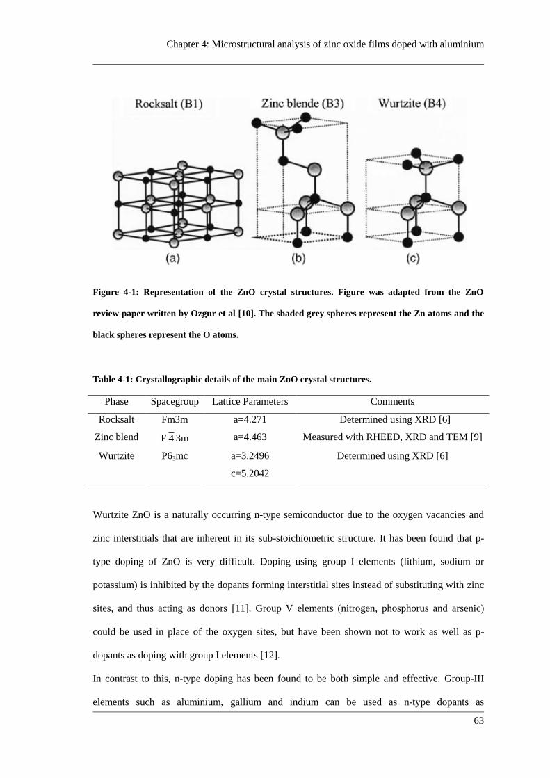
Chapter 4: Microstructural analysis of zinc oxide films doped with aluminium
63
Figure 4-1: Representation of the ZnO crystal structures. Figure was adapted from the ZnO
review paper written by Ozgur et al [10]. The shaded grey spheres represent the Zn atoms and the
black spheres represent the O atoms.
Table 4-1: Crystallographic details of the main ZnO crystal structures.
Phase Spacegroup Lattice Parameters Comments
Rocksalt Fm3m a=4.271 Determined using XRD [6]
Zinc blend F 4 3m a=4.463 Measured with RHEED, XRD and TEM [9]
Wurtzite P63mc a=3.2496
c=5.2042
Determined using XRD [6]
Wurtzite ZnO is a naturally occurring n-type semiconductor due to the oxygen vacancies and
zinc interstitials that are inherent in its sub-stoichiometric structure. It has been found that p-
type doping of ZnO is very difficult. Doping using group I elements (lithium, sodium or
potassium) is inhibited by the dopants forming interstitial sites instead of substituting with zinc
sites, and thus acting as donors [11]. Group V elements (nitrogen, phosphorus and arsenic)
could be used in place of the oxygen sites, but have been shown not to work as well as p-
dopants as doping with group I elements [12].
In contrast to this, n-type doping has been found to be both simple and effective. Group-III
elements such as aluminium, gallium and indium can be used as n-type dopants as
64
substitutional elements for the zinc sites [13-15]. Group-VII elements such as chlorine or iodine
can be used for n-type doping as a substitute for the oxygen position [4, 16]. Of the many
possible n-type dopants available, using aluminium as a dopant in ZnO is a good choice. It has
not only shown promising opto-electrical properties [13, 17-21], but also is cost effective for
extraction and manufacturing, non-toxic and can be exploited as a natural impurity in zinc
metal.
4.1.3 AZO coatings
Growth of AZO films has been performed by many research groups to attain reproducible
TCO’s with the potential to replace ITO [7, 22, 23]. AZO coatings often have a polycrystalline
microstructure with a preferred c-axis crystallographic orientation with respect to the substrate.
For example, Lim et al [18] performed XRD on AZO films prepared using DC magnetron
sputtering and found only the wurtzite (002) peak (c-axis alignment) perpendicular to the
substrate was present. However, the author didn’t specify the phase of the ZnO. Also in this
study, the electrical and optical properties were determined using 4-point probe and optical
transmittance respectively. It was found that the films had a good optical transmittance of
approximately 91.5%, but had a resistivity of 4.3x10⁻⁴ cm, an order of magnitude greater than
that of ITO films.
Lu et al [20] deposited a variety of films also using dc reactive magnetron sputtering with
increasing aluminium content within the target material. It was found that aluminium
concentrations greater than 10% affected the microstructures of the films greatly. Up to 10% Al
concentration the only significant XRD peak was the wurtzite(002) located at 2=34º,
indicating that strong preferred orientation is present in which the c-axis is aligned
perpendicular to the substrate. As the concentration of aluminium is increased above 10%, the
microstructure of the films change. At 15% and 20% aluminium concentrations the XRD shows
additional wurtzite(100) and wurtzite(101) peaks respectively. For Al concentrations >30% the
Chapter 4: Microstructural analysis of zinc oxide films doped with aluminium
65
ZnO(002) peak disappears almost entirely and a Al-metal(113) peak located at approximately
2=44º appears, indicating a two phase system. In this work, electrical characterisation was also
carried out, in which it was found that the minimum resistivity of the AZO films occurs when
an aluminium concentration of 4% is present. For concentrations either side of this, an increase
in the resistivity was observed.
In a paper by Lin et al [19], heavily Al doped (>10%) AZO films were deposited by
simultaneous dc and rf magnetron sputtering. The effect of substrate temperature increase from
room temperature up to 200ºC was investigated. It was found using XRD that the ZnO crystals
growing in the <001>, <102> and <103> directions perpendicular to the substrate were present
in the film. No appreciable shifting in the wurtzite(002) XRD peak was observed, which
indicates an absence of stress generated from the inclusion of Al dopants into the ZnO lattice.
This suggests that the majority of the Al content was located outside of the ZnO (002)
crystallites and was instead forming other Zn-Al phases. This crystallinity was also confirmed
using selected area diffraction in the TEM.
In a paper by Schuler and Aegerter [21] AZO films were deposited using the sol gel dip
coating process where the film thickness was controlled by depositing multiple AZO layers on
top one another. The effect of the number of layers on the microstructure, resistivity and optical
transmittance was studied. Measurements of the resistivity were performed and found to be in
the order of 5x10⁻³
cm, optical measurements yielded approximately 80% transmittance in
the visible region of the spectrum. TEM imaging was also performed on the samples with
differing number of AZO layers and yielded interesting results. For the films deposited by this
method, columnar growth did not occur with the single layer samples, but instead the films
grew as spherical particles 15-25 nm in diameter spread across the substrate. Increase in the
number of layers increased the particle size until eventually at 5-10 layers columnar growth was
present. Thick single layer coatings deposited using this method also appeared as particles, with
66
elongation of the particles in the <001> direction occurring with multilayer films with thick
layers. This paper shows that the thickness of the film has a dramatic effect on the
microstructure of the films, with spherical particles and columnar particles both observed and
shown to yield different physical properties.
Xu et al [24] deposited AZO films at low temperatures by spray pyrolysis. Interestingly the
films had a strong preferred orientation with the <101> direction perpendicular to the substrate
and formed lenticular shaped wurtzite crystals. This is quite unlike most papers (see above) in
which growth usually occurs with the c-axis perpendicular to the substrate. It was found that for
the lowest sheet resistance, an atomic percentage of 4% aluminium was required. This is the
same as what Lu et al [20] found. However in this work, even though the transmission
measurements in the visible region were acceptable (~80% at 550 nm), the resistivities were
quite high. Using a doping concentration of 4% aluminium and post annealing of 550ºC, the
best achievable resistivity was 1×10⁻²
Ω.cm. In contrast to this, the films grown by magnetron
sputtering by Lu et al had much better resistivities (10-4
Ω.cm), high transmittance (~90%) and
had much stronger preferred orientation with the wurtzite c-axis perpendicular to the substrate
and increased crystal size and quality [20].
4.1.4 Presence of negative ions in magnetron sputtering techniques
During reactive deposition using magnetron sputtering and HIPIMS, there is a flux of O- ions
which are generated at the magnetrons and directed towards the deposited film during
deposition along the magnetic field lines. In an experiment by Mráz and Schneider [25] the
energy distribution functions within the chamber during magnetron deposition was determined
using a mass energy analyser and several ion populations were discovered. There was a low
energy ion population which was attributed to dissociative electron attachment of oxygen, in
which the newly formed O- is accelerated towards the substrate by a small fraction of the
magnetron potential. The high energy species are formed from oxygen being sputtered from the
target material as O- and being accelerated towards the substrate and reaching it with an energy
Chapter 4: Microstructural analysis of zinc oxide films doped with aluminium
67
given by the target potential. The medium energy species were found to have energy half that
of the target potential and high energy species. This population was attributed to O2- ions being
accelerated from the target material at full potential, and then dissociating to O- and O with the
energy divided evenly between the species. Hence the O- is detected as having half of the
energy of the target potential. The energy distribution function was also measured for the
possibility of O+ ions within the beam. It was found that this species was present in the beam,
but only as a low energy population with a small intensity. Due to this, it was suggested that
this species does not play a key role in the structure evolution of metal oxide thin films.
This oxygen ion damage effect has been seen in doped zinc oxide films. Minami et al [7]
deposited zinc oxide films doped with Sc and Y using magnetron sputtering. The resistivity,
Hall mobility and carrier concentration of the films was analysed across the surface of the
sample and it was found that these properties were non-uniform. Across the substrate surface
over the magnetron racetrack there were inferior electrical properties such as high resistivity,
low mobility and low carrier concentration.
The work presented in this chapter uses the same pulsed cathodic arc setup employed by
Anders et al [17]. The substrates were heated to 200 ºC during deposition (as it was found to
result in the best resistivity by Anders [17]) and a Zn/Al cathode with 4 at% Al was used. A
more rigorous study of the microstructure is performed by employing XRD, XPS and XAS at
the Australian Synchrotron to directly probe the microstructure electronic structure. It has been
shown that different microstructures can be achieved depending on the deposition technique,
with spherically shaped particles [21], lenticular shaped particles [24] and columnar growth
with c-axis perpendicular to the substrate [18, 20, 21] all being reported. The results presented
in this chapter is a comparison of AZO films prepared using the pulsed arc deposition system to
two other techniques: magnetron sputtering and HIPIMS. By using the same cathode material
for all three deposition methods, a direct comparison between the techniques is presented. Also
presented in this chapter is an investigation of the effect of oxygen ion damage to the films

68
during the deposition of magnetron sputtered and HIPIMS samples. In particular a novel
magnetic filter is used in an attempt to remove O- ion damage.
4.2. Experimental Methods
In this work, four different deposition techniques are used to grow AZO films. Pulsed cathodic
arc deposition grows coatings using a filtered plasma of high energy ions (section 2.1.3),
conventional magnetron sputtering using low energy neutrals (section 2.1.4) and HIPIMS uses
an unfiltered plasma of high energy ions (section 2.1.5). Like the work performed on tungsten
oxide (section 3.1.3), the change in incident energy of the depositing particles is known to have
an important influence on the microstructure of the films [26, 27] which may lead to enhanced
optical or electrical performance. A negative ion filter is introduced into the HIPIMS system
(section 4.2.3) to create a novel deposition technique which may prevent the oxygen ion
damage outlined in section 4.1.4. All of the films were deposited onto both glass microscope
slides and microscope coverslips. A pen mark (<1 mm2 in area) was placed into the corner of
the substrate before deposition, and was later wiped off so that step height analysis using a
profilometer could be performed on the samples to determine the film thickness. Details of the
experimental parameters used in each of these methods are presented below.
4.2.1 Pulsed cathodic arc
Pulsed cathodic arc was used to deposit films with a variety of thicknesses by varying the total
number of pulses to the cathode. The cathode target used was zinc doped with 4% aluminium.
The zinc-aluminum plasma stream passed a 90°-bent open filter to remove most of the
macroparticles. Pure oxygen gas was injected into the chamber using a mass flow controller
(MKS Instruments) and was monitored by a differentially pumped quadrupole mass
spectrometer (model RGA100 by SRS). Arc pulses of 1 ms duration and amplitude of 780 A
were delivered with a repetition rate of usually 3 to 4 pulses per second by a pulse-forming
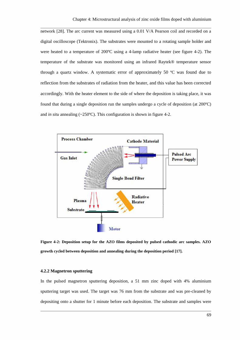
Chapter 4: Microstructural analysis of zinc oxide films doped with aluminium
69
network [28]. The arc current was measured using a 0.01 V/A Pearson coil and recorded on a
digital oscilloscope (Tektronix). The substrates were mounted to a rotating sample holder and
were heated to a temperature of 200ºC using a 4-lamp radiative heater (see figure 4-2). The
temperature of the substrate was monitored using an infrared Raytek® temperature sensor
through a quartz window. A systematic error of approximately 50 ºC was found due to
reflection from the substrates of radiation from the heater, and this value has been corrected
accordingly. With the heater element to the side of where the deposition is taking place, it was
found that during a single deposition run the samples undergo a cycle of deposition (at 200ºC)
and in situ annealing (~250ºC). This configuration is shown in figure 4-2.
Figure 4-2: Deposition setup for the AZO films deposited by pulsed cathodic arc samples. AZO
growth cycled between deposition and annealing during the deposition period [17].
4.2.2 Magnetron sputtering
In the pulsed magnetron sputtering deposition, a 51 mm zinc doped with 4% aluminium
sputtering target was used. The target was 76 mm from the substrate and was pre-cleaned by
depositing onto a shutter for 1 minute before each deposition. The substrate and samples were
70
heated to ~200 ºC using a 4 lamp radiative heater during deposition. The magnetron was a 50
mm close-to-balanced magnetron with modified connectors to allow for a high peak current of
up to 500 A. The power supply was run in pulsed DC with 100 kHz pulse rate, 736 ns off time
(+ve pulse) per cycle with an operating power of 75 W. The oxygen gas flow was adjusted to
60 sccm Ar, 36% O2 (total pressure 7.5 mTorr) during the run to maintain a near constant
operating voltage of 311-315 V.
4.2.3 High power impulse magnetron sputtering (HIPIMS)
For the HIPIMS samples, the same 4% aluminium doped zinc target was used as with the
magnetron setup. Current pulses were supplied by an upgraded SPIK 2000A pulser, with a
charging voltage up to 1000 V and pulse length of typically 400 µs. The total pressure within
the chamber for all experiments was typically 1 Pa (7 mTorr). The magnetron was a 5 cm close-
to-balanced magnetron that was placed 210 mm from the substrate. The substrate and samples
were heated to ~200ºC using a 4-lamp radiative heater as this temperature was found to provide
the best films for this setup [17].
4.2.4 Negative ion filter in magnetron deposition
To combat the effect of film degradation due to the geometry of the magnetron racetrack a
simple straight line magnetic filter was introduced into the HIPIMS setup between the
magnetron and the substrate. The filter setup is shown in figure 4-3. This acts to change the
trajectory of the negative ions in the beam to force them away from the substrate and the AZO
film being deposited. It will also act to focus the positive ions (for example our aluminium and
zinc ions) towards the substrate, increasing the deposition rate. To test the effect of the ion filter
on HIPIMS deposition, two samples were prepared. The first sample was prepared using the
same setup as in section 4.2.3, but with the inclusion of the straight magnetic filter. A sufficient
number of pulses to achieve a thickness of approximately 200 nm was chosen. The second
sample was prepared in the exact same way, with the same number of pulses, but without the
inclusion of the filter.
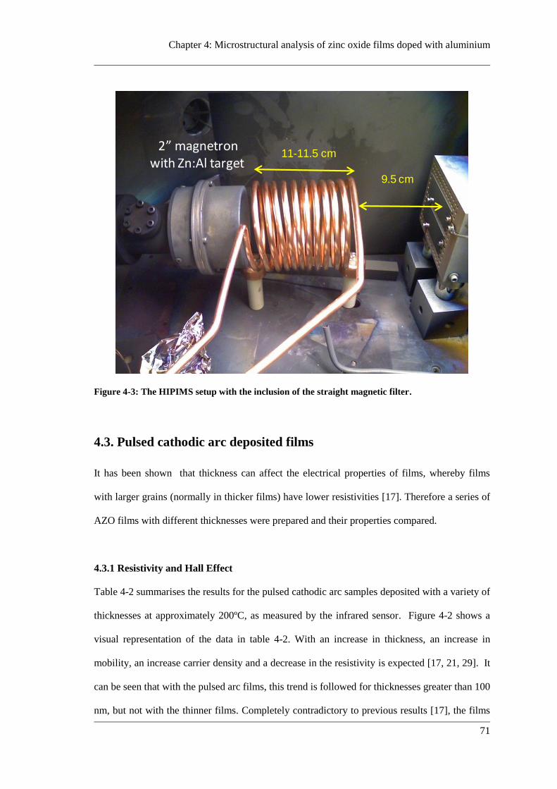
Chapter 4: Microstructural analysis of zinc oxide films doped with aluminium
71
11-11.5 cm
9.5 cm
2” magnetron with Zn:Al target
Figure 4-3: The HIPIMS setup with the inclusion of the straight magnetic filter.
4.3. Pulsed cathodic arc deposited films
It has been shown that thickness can affect the electrical properties of films, whereby films
with larger grains (normally in thicker films) have lower resistivities [17]. Therefore a series of
AZO films with different thicknesses were prepared and their properties compared.
4.3.1 Resistivity and Hall Effect
Table 4-2 summarises the results for the pulsed cathodic arc samples deposited with a variety of
thicknesses at approximately 200ºC, as measured by the infrared sensor. Figure 4-2 shows a
visual representation of the data in table 4-2. With an increase in thickness, an increase in
mobility, an increase carrier density and a decrease in the resistivity is expected [17, 21, 29]. It
can be seen that with the pulsed arc films, this trend is followed for thicknesses greater than 100
nm, but not with the thinner films. Completely contradictory to previous results [17], the films
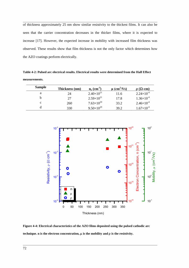
72
of thickness approximately 25 nm show similar resistivity to the thickest films. It can also be
seen that the carrier concentration decreases in the thicker films, where it is expected to
increase [17]. However, the expected increase in mobility with increased film thickness was
observed. These results show that film thickness is not the only factor which determines how
the AZO coatings perform electrically.
Table 4-2: Pulsed arc electrical results. Electrical results were determined from the Hall Effect
measurements.
Sample Thickness (nm) ne (cm
-3) μ (cm
2/Vs) -cm)
a 24 2.40×10²¹
11.6 2.24×10⁻⁴
b 27 2.59×10²¹
17.8 1.36×10⁻⁴
c 260 7.63×10²⁰
33.2 2.46×10⁻⁴
d 330 9.50×10²⁰
39.2 1.67×10⁻⁴
0 50 100 150 200 250 300 350
1018
1019
1020
1021
1022
Ele
ctr
on
Co
nce
ntr
atio
n,
n (
cm
-3)
Thickness (nm)
10-1
100
101
102
Re
sis
tivity, (
cm
-1)
Mo
bili
ty, (
cm
2/V
s)
10-5
10-4
10-3
10-2
n
Figure 4-4: Electrical characteristics of the AZO films deposited using the pulsed cathodic arc
technique. n is the electron concentration, is the mobility and is the resistivity.
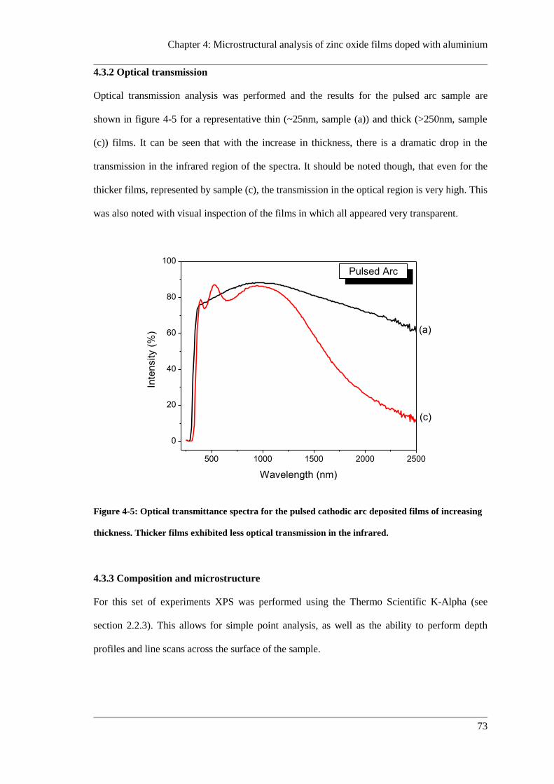
Chapter 4: Microstructural analysis of zinc oxide films doped with aluminium
73
4.3.2 Optical transmission
Optical transmission analysis was performed and the results for the pulsed arc sample are
shown in figure 4-5 for a representative thin (~25nm, sample (a)) and thick (>250nm, sample
(c)) films. It can be seen that with the increase in thickness, there is a dramatic drop in the
transmission in the infrared region of the spectra. It should be noted though, that even for the
thicker films, represented by sample (c), the transmission in the optical region is very high. This
was also noted with visual inspection of the films in which all appeared very transparent.
500 1000 1500 2000 2500
0
20
40
60
80
100
(c)
(a)
Pulsed Arc
Inte
nsity (
%)
Wavelength (nm)
Figure 4-5: Optical transmittance spectra for the pulsed cathodic arc deposited films of increasing
thickness. Thicker films exhibited less optical transmission in the infrared.
4.3.3 Composition and microstructure
For this set of experiments XPS was performed using the Thermo Scientific K-Alpha (see
section 2.2.3). This allows for simple point analysis, as well as the ability to perform depth
profiles and line scans across the surface of the sample.
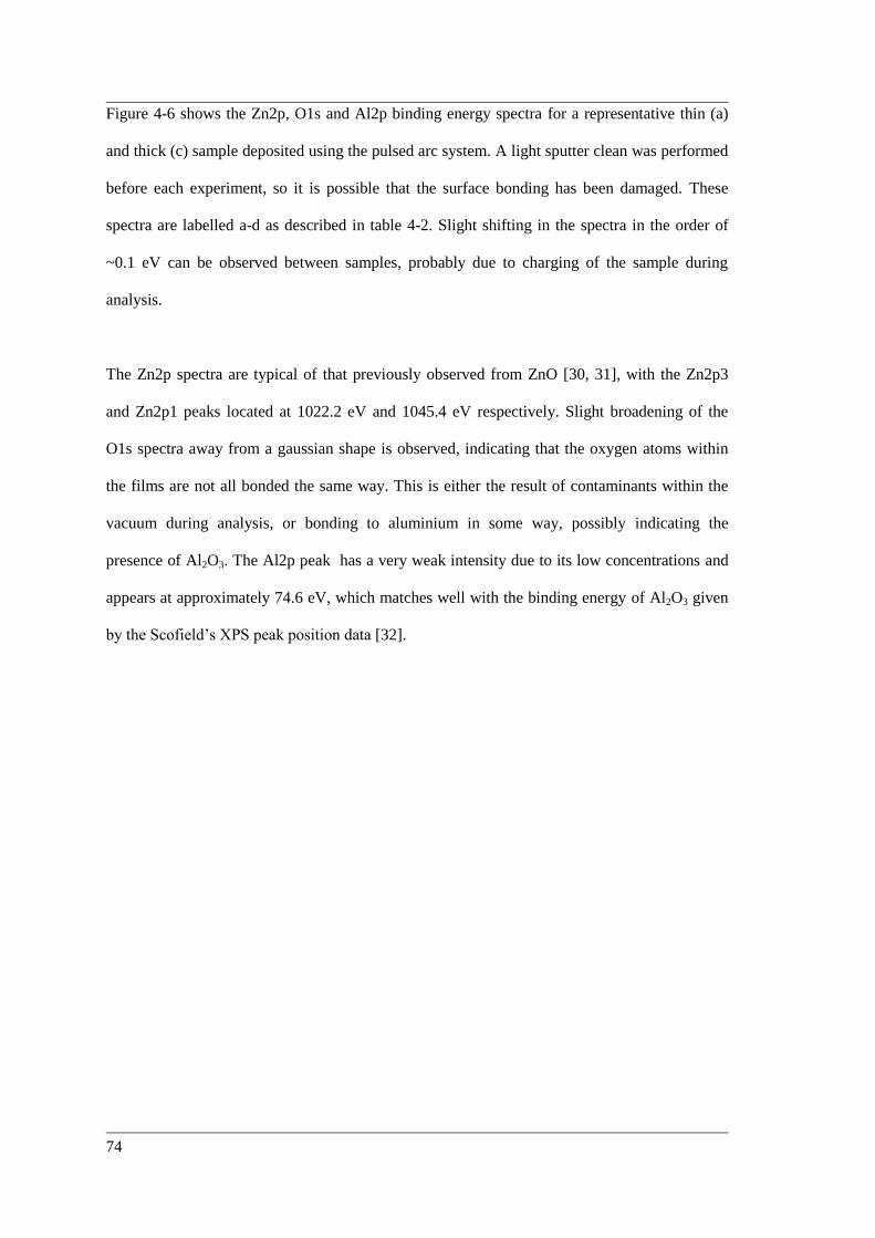
74
Figure 4-6 shows the Zn2p, O1s and Al2p binding energy spectra for a representative thin (a)
and thick (c) sample deposited using the pulsed arc system. A light sputter clean was performed
before each experiment, so it is possible that the surface bonding has been damaged. These
spectra are labelled a-d as described in table 4-2. Slight shifting in the spectra in the order of
~0.1 eV can be observed between samples, probably due to charging of the sample during
analysis.
The Zn2p spectra are typical of that previously observed from ZnO [30, 31], with the Zn2p3
and Zn2p1 peaks located at 1022.2 eV and 1045.4 eV respectively. Slight broadening of the
O1s spectra away from a gaussian shape is observed, indicating that the oxygen atoms within
the films are not all bonded the same way. This is either the result of contaminants within the
vacuum during analysis, or bonding to aluminium in some way, possibly indicating the
presence of Al2O3. The Al2p peak has a very weak intensity due to its low concentrations and
appears at approximately 74.6 eV, which matches well with the binding energy of Al2O3 given
by the Scofield’s XPS peak position data [32].
Chapter 4: Microstructural analysis of zinc oxide films doped with aluminium
75
1050 1040 1030 1020
Inte
nsity (
arb
. units)
Binding energy (eV)
(c)
(a)
Zn2p
544 540 536 532 528
O1s
Inte
nsity (
arb
. units)
Binding Energy (eV)
(c)
(a)
85 80 75 70 65
In
ten
sity (
arb
. u
nits)
Binding Energy (eV)
(c)
(a)
Al2p
Figure 4-6: XPS scans of the indicated
pulsed cathodic arc films in the vicinity
of the Zn2p, O1s and Al2p binding
energies. The peak positions are typical
of ZnO thin film coatings.
Using the normalised peak area and sensitivity factors we determine the atomic percentages of
the elements within the coatings. Table 4-3 shows the stoichiometry results for the pulsed
cathodic arc films of varying thicknesses. It can be seen with these films that the overall
aluminium concentration of the films stays approximately the same as that found within the
cathode material. All of the films were found to be oxygen deficient, possibly due to
preferential oxygen sputtering during the sputter cleaning with Ar+ ions. [33]
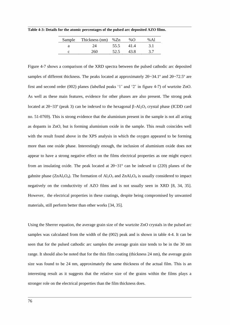
76
Table 4-3: Details for the atomic percentages of the pulsed arc deposited AZO films.
Sample Thickness (nm) %Zn %O %Al
a 24 55.5 41.4 3.1
c 260 52.5 43.8 3.7
Figure 4-7 shows a comparison of the XRD spectra between the pulsed cathodic arc deposited
samples of different thickness. The peaks located at approximately 2~34.1º and 2~72.5º are
first and second order (002) planes (labelled peaks ‘1’ and ‘2’ in figure 4-7) of wurtzite ZnO.
As well as these main features, evidence for other phases are also present. The strong peak
located at 2~33º (peak 3) can be indexed to the hexagonal -Al2O3 crystal phase (ICDD card
no. 51-0769). This is strong evidence that the aluminium present in the sample is not all acting
as dopants in ZnO, but is forming aluminium oxide in the sample. This result coincides well
with the result found above in the XPS analysis in which the oxygen appeared to be forming
more than one oxide phase. Interestingly enough, the inclusion of aluminium oxide does not
appear to have a strong negative effect on the films electrical properties as one might expect
from an insulating oxide. The peak located at 2~31º can be indexed to (220) planes of the
gahnite phase (ZnAl2O4). The formation of Al2O3 and ZnAl2O4 is usually considered to impact
negatively on the conductivity of AZO films and is not usually seen in XRD [8, 34, 35].
However, the electrical properties in these coatings, despite being compromised by unwanted
materials, still perform better than other works [34, 35].
Using the Sherrer equation, the average grain size of the wurtzite ZnO crystals in the pulsed arc
samples was calculated from the width of the (002) peak and is shown in table 4-4. It can be
seen that for the pulsed cathodic arc samples the average grain size tends to be in the 30 nm
range. It should also be noted that for the thin film coating (thickness 24 nm), the average grain
size was found to be 24 nm, approximately the same thickness of the actual film. This is an
interesting result as it suggests that the relative size of the grains within the films plays a
stronger role on the electrical properties than the film thickness does.
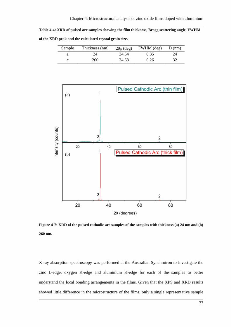
Chapter 4: Microstructural analysis of zinc oxide films doped with aluminium
77
Table 4-4: XRD of pulsed arc samples showing the film thickness, Bragg scattering angle, FWHM
of the XRD peak and the calculated crystal grain size.
Sample Thickness (nm) 2B (deg) FWHM (deg) D (nm)
a 24 34.54 0.35 24
c 260 34.68 0.26 32
20 40 60 80
20 40 60 80
In
ten
sity (
co
un
ts)
23
1
2 (degrees)
Pulsed Cathodic Arc (thick film)
Pulsed Cathodic Arc (thin film)
23
1
Figure 4-7: XRD of the pulsed cathodic arc samples of the samples with thickness (a) 24 nm and (b)
260 nm.
X-ray absorption spectroscopy was performed at the Australian Synchrotron to investigate the
zinc L-edge, oxygen K-edge and aluminium K-edge for each of the samples to better
understand the local bonding arrangements in the films. Given that the XPS and XRD results
showed little difference in the microstructure of the films, only a single representative sample
(a)
(b)
78
(c) was selected for this experiment. Figure 4-8a shows the aluminium K-edge for the AZO
coating with a thickness of 260 nm. The peaks located at approximately 1567.4 eV and 1571.5
eV refer to the lag to eu transition and the multiple scattering contributions respectively [5]. The
peak at 1567.4 eV is characteristic of distorted octahedral coordination (AlO6, with 6 fold
symmetry) of the aluminium atoms with the surrounding oxygen environment [5, 36]. The peak
characteristic of tetrahedral coordination (located at approximately 1565.4 eV) is not present
within these films [5, 36]. This result supports the XPS and XRD results in which it was found
that the aluminium was appearing as aluminium oxide (Al2O3) and not as a dopant.
Figure 4-8b shows the XAS in the region of the oxygen K-edge for the pulsed arc deposited
coating. The only prominent feature in the spectrum is a broad peak at approximately 538 eV
due to transitions of the O1s electrons to the O2p and Zn4sp hybrid orbital. The peaks relating
to the O1s to O2p and Zn3d orbitals are present because of the d10
configuration of ZnO [37].
Also shown in this figure is the oxygen K-edge calculated for wurtzite ZnO using the FEFF9
code. It can be seen that there is extra broadening of features in the pulsed arc XANES, making
the transition peak appear washed out. This is possibly due to the inclusion of oxygen K-edge
contributions from Al2O3 or other oxidised Zn/Al phases. Figure 4-8c shows the XAS spectrum
in the region of the zinc L-edges. The energy positions and shape of the spectra match well with
that previously reported for ZnO using XANES [38].
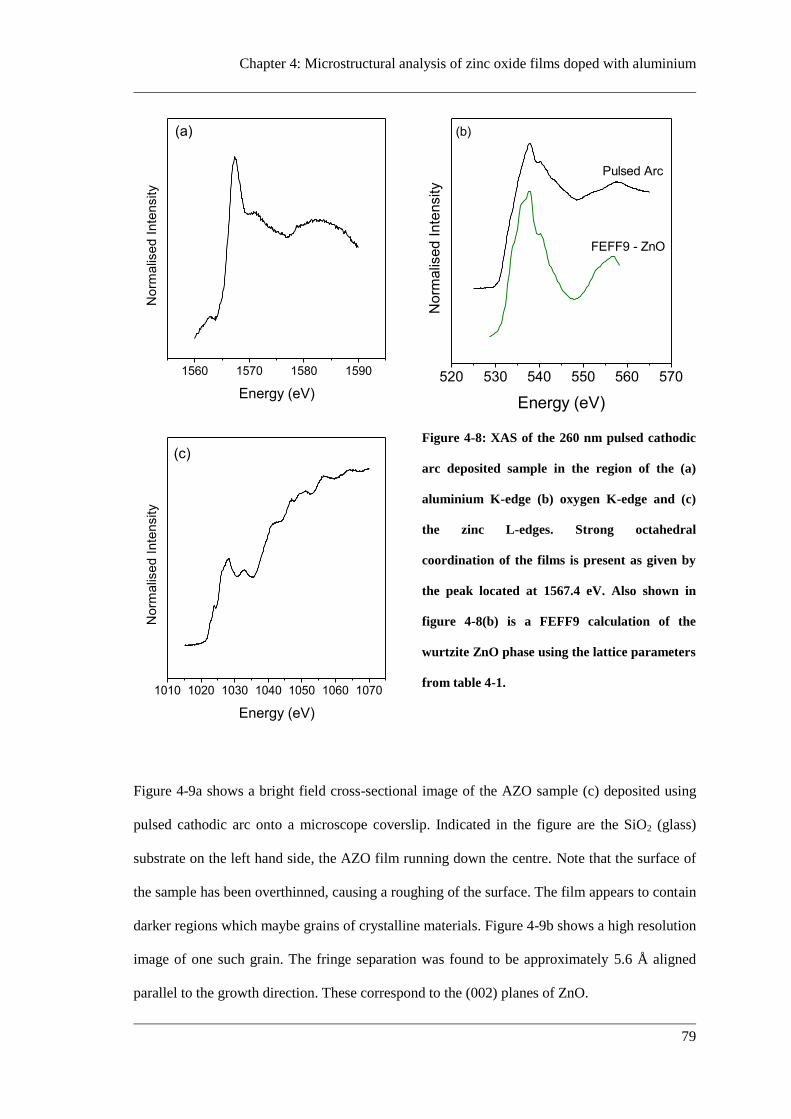
Chapter 4: Microstructural analysis of zinc oxide films doped with aluminium
79
1560 1570 1580 1590
No
rma
lise
d I
nte
nsity
Energy (eV)
(a)
520 530 540 550 560 570
(b)
No
rma
lise
d I
nte
nsity
Energy (eV)
Pulsed Arc
FEFF9 - ZnO
1010 1020 1030 1040 1050 1060 1070
No
rma
lise
d I
nte
nsity
Energy (eV)
(c)
Figure 4-8: XAS of the 260 nm pulsed cathodic
arc deposited sample in the region of the (a)
aluminium K-edge (b) oxygen K-edge and (c)
the zinc L-edges. Strong octahedral
coordination of the films is present as given by
the peak located at 1567.4 eV. Also shown in
figure 4-8(b) is a FEFF9 calculation of the
wurtzite ZnO phase using the lattice parameters
from table 4-1.
Figure 4-9a shows a bright field cross-sectional image of the AZO sample (c) deposited using
pulsed cathodic arc onto a microscope coverslip. Indicated in the figure are the SiO2 (glass)
substrate on the left hand side, the AZO film running down the centre. Note that the surface of
the sample has been overthinned, causing a roughing of the surface. The film appears to contain
darker regions which maybe grains of crystalline materials. Figure 4-9b shows a high resolution
image of one such grain. The fringe separation was found to be approximately 5.6 Å aligned
parallel to the growth direction. These correspond to the (002) planes of ZnO.

80
The indexed diffraction pattern for this area is shown in figure 4-10 (left). The diffraction
pattern itself is comprised of a combination of diffraction patterns each from crystal grains with
strong c-axis <001> orientation (as seen by the strong intensity of the respective spots)
perpendicular to the surface. Each of these grains has a different amount of rotation around the
c-axis, so we observe diffraction patterns from different Laue zones simultaneously. Figure 4-
10 (right) shows the indexing of the diffraction pattern from 3 different Laue zones ([110] [210]
and [310]) and a molecular representation (left) of the orientation of the particular grains as
calculated using the JEMS software package [39].
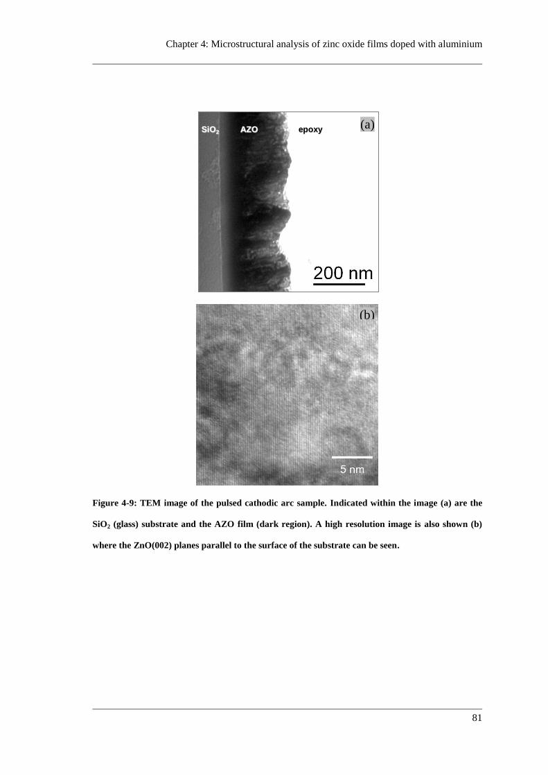
Chapter 4: Microstructural analysis of zinc oxide films doped with aluminium
81
SiO2 AZO epoxy
Figure 4-9: TEM image of the pulsed cathodic arc sample. Indicated within the image (a) are the
SiO2 (glass) substrate and the AZO film (dark region). A high resolution image is also shown (b)
where the ZnO(002) planes parallel to the surface of the substrate can be seen.
(a)
(b)
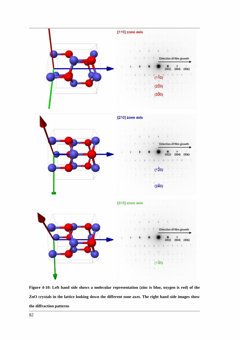
82
Figure 4-10: Left hand side shows a molecular representation (zinc is blue, oxygen is red) of the
ZnO crystals in the lattice looking down the different zone axes. The right hand side images show
the diffraction patterns
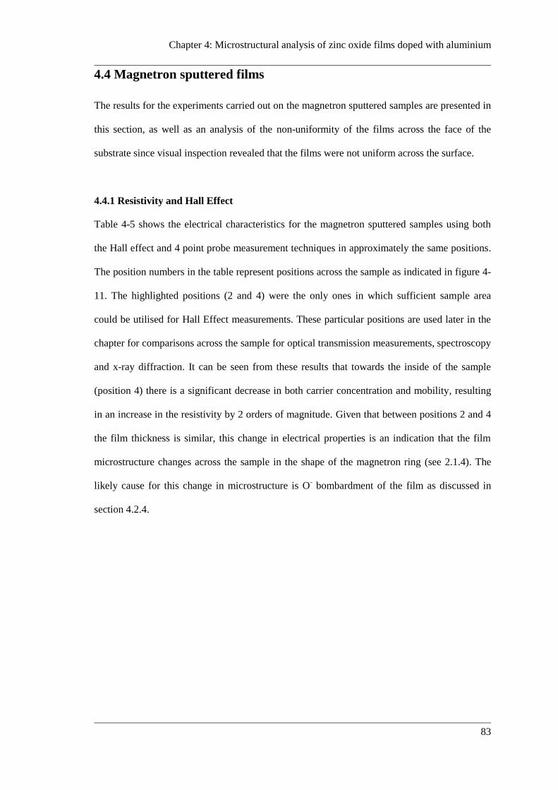
Chapter 4: Microstructural analysis of zinc oxide films doped with aluminium
83
4.4 Magnetron sputtered films
The results for the experiments carried out on the magnetron sputtered samples are presented in
this section, as well as an analysis of the non-uniformity of the films across the face of the
substrate since visual inspection revealed that the films were not uniform across the surface.
4.4.1 Resistivity and Hall Effect
Table 4-5 shows the electrical characteristics for the magnetron sputtered samples using both
the Hall effect and 4 point probe measurement techniques in approximately the same positions.
The position numbers in the table represent positions across the sample as indicated in figure 4-
11. The highlighted positions (2 and 4) were the only ones in which sufficient sample area
could be utilised for Hall Effect measurements. These particular positions are used later in the
chapter for comparisons across the sample for optical transmission measurements, spectroscopy
and x-ray diffraction. It can be seen from these results that towards the inside of the sample
(position 4) there is a significant decrease in both carrier concentration and mobility, resulting
in an increase in the resistivity by 2 orders of magnitude. Given that between positions 2 and 4
the film thickness is similar, this change in electrical properties is an indication that the film
microstructure changes across the sample in the shape of the magnetron ring (see 2.1.4). The
likely cause for this change in microstructure is O- bombardment of the film as discussed in
section 4.2.4.
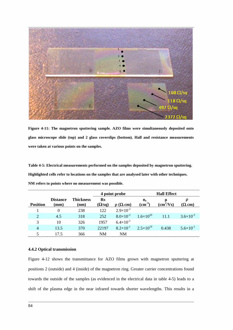
84
Figure 4-11: The magnetron sputtering sample. AZO films were simultaneously deposited onto
glass microscope slide (top) and 2 glass coverslips (bottom). Hall and resistance measurements
were taken at various points on the samples.
Table 4-5: Electrical measurements performed on the samples deposited by magnetron sputtering.
Highlighted cells refer to locations on the samples that are analysed later with other techniques.
NM refers to points where no measurement was possible.
4 point probe Hall Effect
Position
Distance
(mm)
Thickness
(nm)
Rs
(Ω/sq) cm)
ne
(cm-3
)
μ
(cm2/Vs)
cm)
1 0 238 122 2.9×10⁻³
2 4.5 318 252 8.0×10⁻³
1.6×10²⁰
11.1 3.6×10⁻³
3 10 326 1957 6.4×10⁻²
4 13.5 370 22197 8.2×10⁻¹
2.5×10¹⁹
0.438 5.6×10⁻¹
5 17.5 366 NM NM
4.4.2 Optical transmission
Figure 4-12 shows the transmittance for AZO films grown with magnetron sputtering at
positions 2 (outside) and 4 (inside) of the magnetron ring. Greater carrier concentrations found
towards the outside of the samples (as evidenced in the electrical data in table 4-5) leads to a
shift of the plasma edge in the near infrared towards shorter wavelengths. This results in a
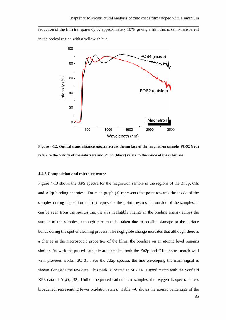
Chapter 4: Microstructural analysis of zinc oxide films doped with aluminium
85
reduction of the film transparency by approximately 10%, giving a film that is semi-transparent
in the optical region with a yellowish hue.
500 1000 1500 2000 2500
0
20
40
60
80
100
POS4 (inside)
POS2 (outside)
Magnetron
Inte
nsity (
%)
Wavelength (nm)
Figure 4-12: Optical transmittance spectra across the surface of the magnetron sample. POS2 (red)
refers to the outside of the substrate and POS4 (black) refers to the inside of the substrate
4.4.3 Composition and microstructure
Figure 4-13 shows the XPS spectra for the magnetron sample in the regions of the Zn2p, O1s
and Al2p binding energies. For each graph (a) represents the point towards the inside of the
samples during deposition and (b) represents the point towards the outside of the samples. It
can be seen from the spectra that there is negligible change in the binding energy across the
surface of the samples, although care must be taken due to possible damage to the surface
bonds during the sputter cleaning process. The negligible change indicates that although there is
a change in the macroscopic properties of the films, the bonding on an atomic level remains
similar. As with the pulsed cathodic arc samples, both the Zn2p and O1s spectra match well
with previous works [30, 31]. For the Al2p spectra, the line enveloping the main signal is
shown alongside the raw data. This peak is located at 74.7 eV, a good match with the Scofield
XPS data of Al2O3 [32]. Unlike the pulsed cathodic arc samples, the oxygen 1s spectra is less
broadened, representing fewer oxidation states. Table 4-6 shows the atomic percentage of the
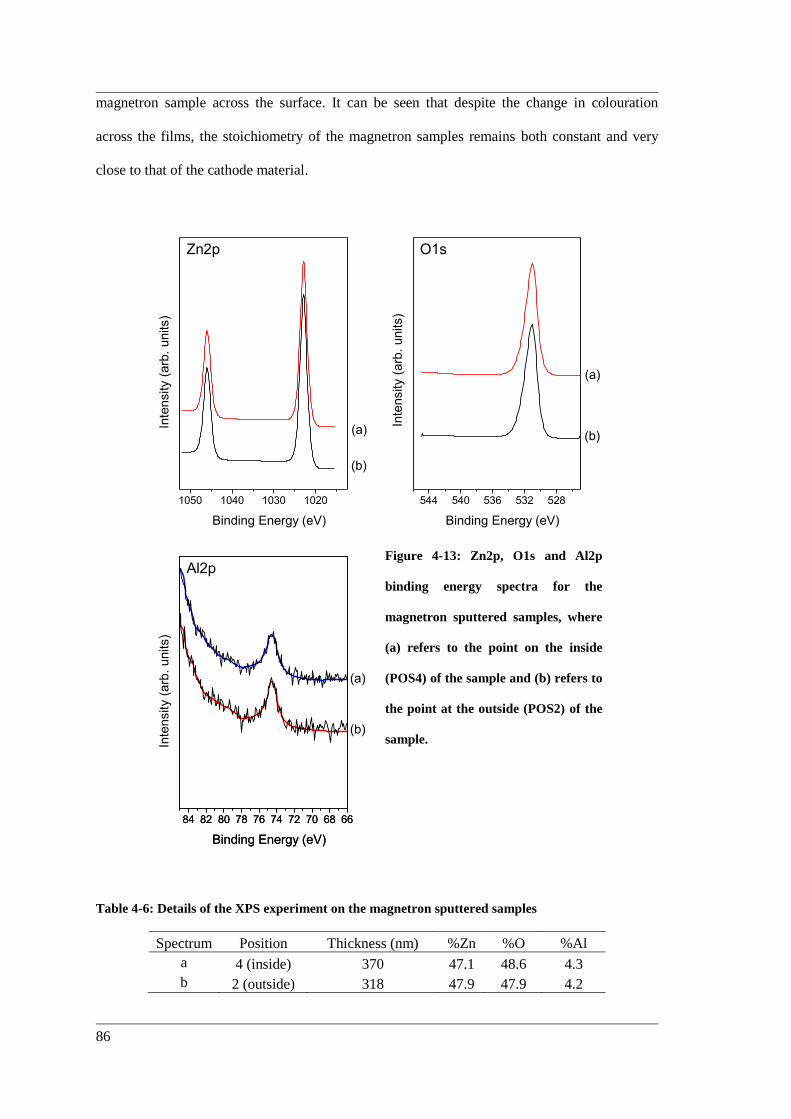
86
magnetron sample across the surface. It can be seen that despite the change in colouration
across the films, the stoichiometry of the magnetron samples remains both constant and very
close to that of the cathode material.
1050 1040 1030 1020
Zn2p
Inte
nsity (
arb
. units)
Binding Energy (eV)
(b)
(a)
544 540 536 532 528
O1s
Inte
nsity (
arb
. units)
Binding Energy (eV)
(b)
(a)
84 82 80 78 76 74 72 70 68 6684 82 80 78 76 74 72 70 68 66
Inte
nsity (
arb
. u
nits)
Binding Energy (eV)Binding Energy (eV)
Al2p
(a)
(b)
Figure 4-13: Zn2p, O1s and Al2p
binding energy spectra for the
magnetron sputtered samples, where
(a) refers to the point on the inside
(POS4) of the sample and (b) refers to
the point at the outside (POS2) of the
sample.
Table 4-6: Details of the XPS experiment on the magnetron sputtered samples
Spectrum Position Thickness (nm) %Zn %O %Al
a 4 (inside) 370 47.1 48.6 4.3
b 2 (outside) 318 47.9 47.9 4.2
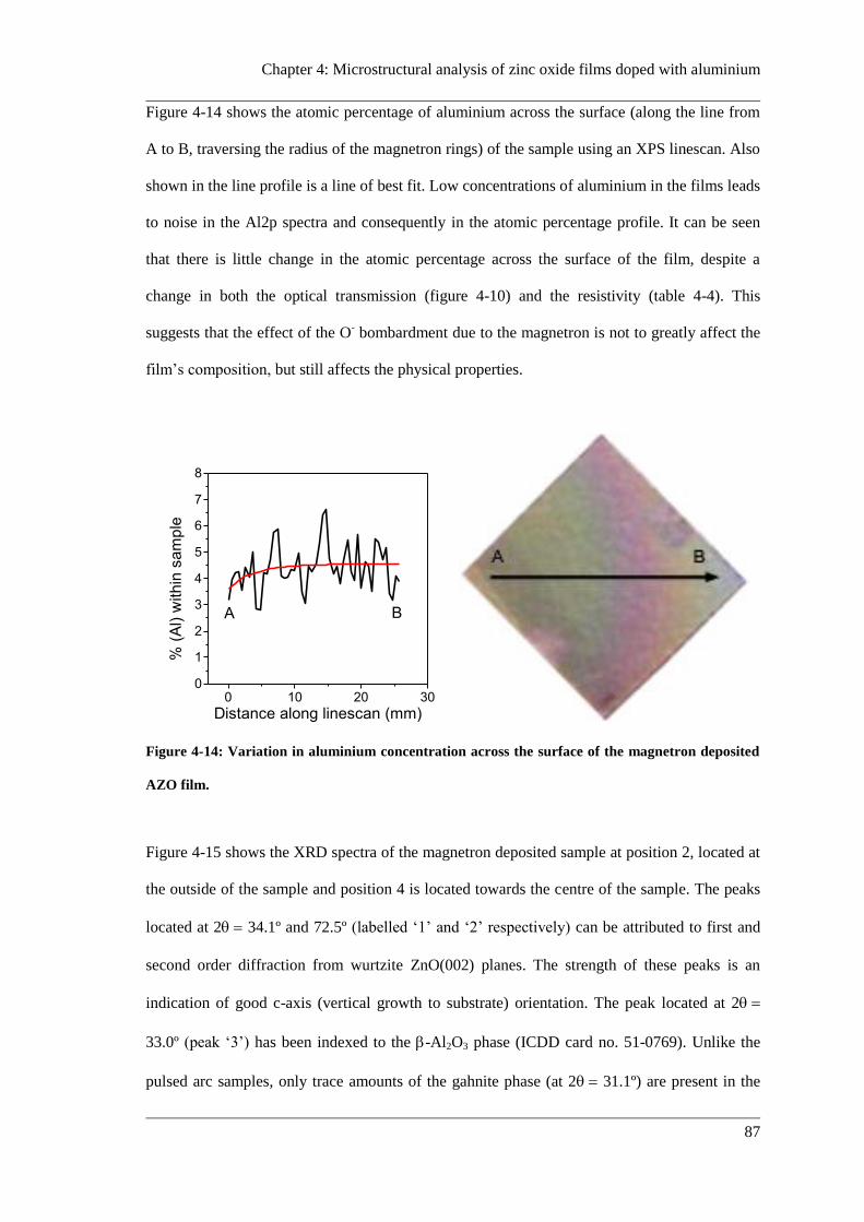
Chapter 4: Microstructural analysis of zinc oxide films doped with aluminium
87
Figure 4-14 shows the atomic percentage of aluminium across the surface (along the line from
A to B, traversing the radius of the magnetron rings) of the sample using an XPS linescan. Also
shown in the line profile is a line of best fit. Low concentrations of aluminium in the films leads
to noise in the Al2p spectra and consequently in the atomic percentage profile. It can be seen
that there is little change in the atomic percentage across the surface of the film, despite a
change in both the optical transmission (figure 4-10) and the resistivity (table 4-4). This
suggests that the effect of the O- bombardment due to the magnetron is not to greatly affect the
film’s composition, but still affects the physical properties.
0 10 20 300
1
2
3
4
5
6
7
8
% (
Al) w
ithin
sam
ple
Distance along linescan (mm)
BA
Figure 4-14: Variation in aluminium concentration across the surface of the magnetron deposited
AZO film.
Figure 4-15 shows the XRD spectra of the magnetron deposited sample at position 2, located at
the outside of the sample and position 4 is located towards the centre of the sample. The peaks
located at 2 34.1º and 72.5º (labelled ‘1’ and ‘2’ respectively) can be attributed to first and
second order diffraction from wurtzite ZnO(002) planes. The strength of these peaks is an
indication of good c-axis (vertical growth to substrate) orientation. The peak located at 2
33.0º (peak ‘3’) has been indexed to the -Al2O3 phase (ICDD card no. 51-0769). Unlike the
pulsed arc samples, only trace amounts of the gahnite phase (at 2 31.1º) are present in the
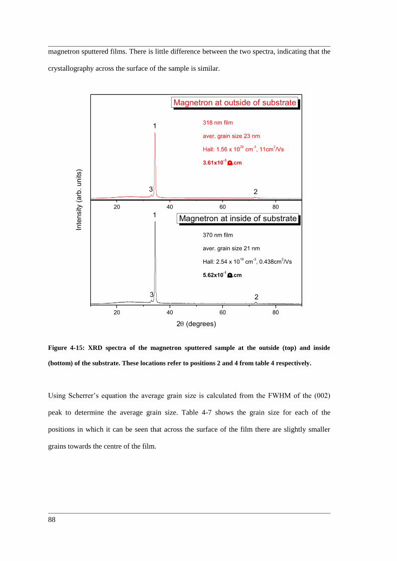
88
magnetron sputtered films. There is little difference between the two spectra, indicating that the
crystallography across the surface of the sample is similar.
20 40 60 80
20 40 60 80
318 nm film
aver. grain size 23 nm
Hall: 1.56 x 10²⁰
cm-3, 11cm
2/Vs
3.61x10⁻³ .cm
370 nm film
aver. grain size 21 nm
Hall: 2.54 x 10¹⁹
cm-3, 0.438cm
2/Vs
5.62x10⁻¹ .cm
23
Magnetron at inside of substrate
Magnetron at outside of substrate
Inte
nsity (
arb
. u
nits)
1
2 (degrees)
23
1
Figure 4-15: XRD spectra of the magnetron sputtered sample at the outside (top) and inside
(bottom) of the substrate. These locations refer to positions 2 and 4 from table 4 respectively.
Using Scherrer’s equation the average grain size is calculated from the FWHM of the (002)
peak to determine the average grain size. Table 4-7 shows the grain size for each of the
positions in which it can be seen that across the surface of the film there are slightly smaller
grains towards the centre of the film.
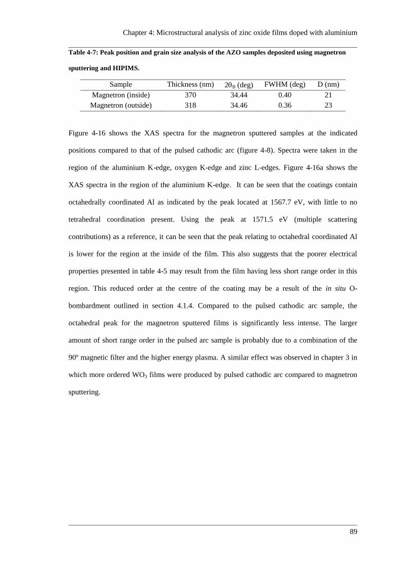
Chapter 4: Microstructural analysis of zinc oxide films doped with aluminium
89
Table 4-7: Peak position and grain size analysis of the AZO samples deposited using magnetron
sputtering and HIPIMS.
Sample Thickness (nm) 2B (deg) FWHM (deg) D (nm)
Magnetron (inside) 370 34.44 0.40 21
Magnetron (outside) 318 34.46 0.36 23
Figure 4-16 shows the XAS spectra for the magnetron sputtered samples at the indicated
positions compared to that of the pulsed cathodic arc (figure 4-8). Spectra were taken in the
region of the aluminium K-edge, oxygen K-edge and zinc L-edges. Figure 4-16a shows the
XAS spectra in the region of the aluminium K-edge. It can be seen that the coatings contain
octahedrally coordinated Al as indicated by the peak located at 1567.7 eV, with little to no
tetrahedral coordination present. Using the peak at 1571.5 eV (multiple scattering
contributions) as a reference, it can be seen that the peak relating to octahedral coordinated Al
is lower for the region at the inside of the film. This also suggests that the poorer electrical
properties presented in table 4-5 may result from the film having less short range order in this
region. This reduced order at the centre of the coating may be a result of the in situ O-
bombardment outlined in section 4.1.4. Compared to the pulsed cathodic arc sample, the
octahedral peak for the magnetron sputtered films is significantly less intense. The larger
amount of short range order in the pulsed arc sample is probably due to a combination of the
90º magnetic filter and the higher energy plasma. A similar effect was observed in chapter 3 in
which more ordered WO3 films were produced by pulsed cathodic arc compared to magnetron
sputtering.
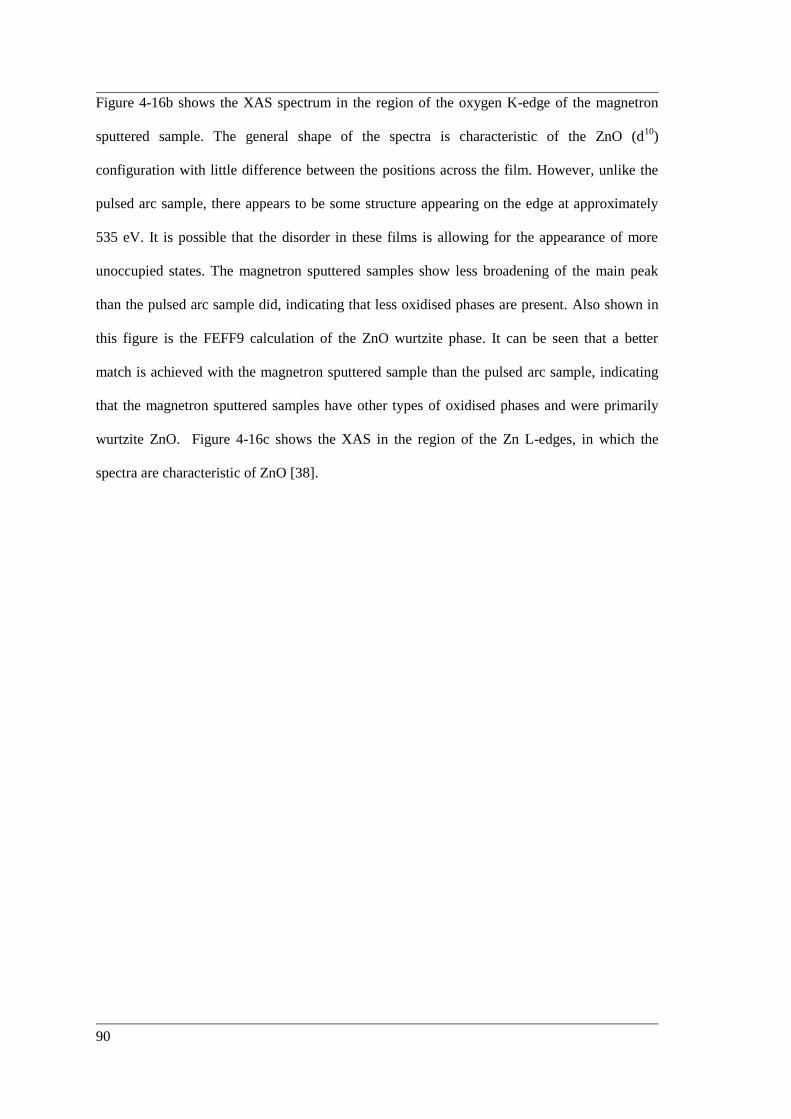
90
Figure 4-16b shows the XAS spectrum in the region of the oxygen K-edge of the magnetron
sputtered sample. The general shape of the spectra is characteristic of the ZnO (d10
)
configuration with little difference between the positions across the film. However, unlike the
pulsed arc sample, there appears to be some structure appearing on the edge at approximately
535 eV. It is possible that the disorder in these films is allowing for the appearance of more
unoccupied states. The magnetron sputtered samples show less broadening of the main peak
than the pulsed arc sample did, indicating that less oxidised phases are present. Also shown in
this figure is the FEFF9 calculation of the ZnO wurtzite phase. It can be seen that a better
match is achieved with the magnetron sputtered sample than the pulsed arc sample, indicating
that the magnetron sputtered samples have other types of oxidised phases and were primarily
wurtzite ZnO. Figure 4-16c shows the XAS in the region of the Zn L-edges, in which the
spectra are characteristic of ZnO [38].
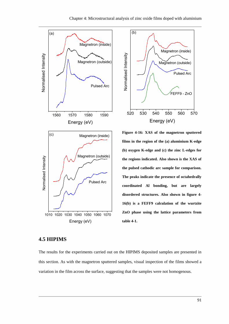
Chapter 4: Microstructural analysis of zinc oxide films doped with aluminium
91
1560 1570 1580 1590
(a)
Magnetron (outside)
No
rma
lise
d I
nte
nsity
Energy (eV)
Magnetron (inside)
Pulsed Arc
520 530 540 550 560 570
Magnetron (outside)
(b)
Pulsed Arc
No
rma
lise
d I
nte
nsity
Energy (eV)
FEFF9 - ZnO
Magnetron (inside)
1010 1020 1030 1040 1050 1060 1070
(c)
Magnetron (outside)
No
rma
lise
d I
nte
nsity
Energy (eV)
Pulsed Arc
Magnetron (inside)
Figure 4-16: XAS of the magnetron sputtered
films in the region of the (a) aluminium K-edge
(b) oxygen K-edge and (c) the zinc L-edges for
the regions indicated. Also shown is the XAS of
the pulsed cathodic arc sample for comparison.
The peaks indicate the presence of octahedrally
coordinated Al bonding, but are largely
disordered structures. Also shown in figure 4-
16(b) is a FEFF9 calculation of the wurtzite
ZnO phase using the lattice parameters from
table 4-1.
4.5 HIPIMS
The results for the experiments carried out on the HIPIMS deposited samples are presented in
this section. As with the magnetron sputtered samples, visual inspection of the films showed a
variation in the film across the surface, suggesting that the samples were not homogenous.

92
4.5.1 Resistivity and Hall Effect
Table 4-8 shows the electrical characteristics of the sample deposited using the HIPIMS
technique. 4 point probe and Hall effect measurements were taken in appoximately the same
positions. The ‘position’ shown in the table refers to locations on the surface of the sample
indicated in figure 4-17, where the main points of interest position 1 and position 3 are located
at the outside and inside of the sample respectively. From the results a similar trend to that of
the magnetron sputtered samples can be seen. At the outside of the sample superior electrical
characteristics are seen, with a greater carrier concentration, greater mobility and a lesser
resistivity.
Figure 4-18 shows the change in the resistivity across the surface of the sample. It can be seen
that there is a dramatic increase in the resitivity towards the centre of the sample (positions 3
and 4). It is possible that large amounts of O- ion damage, as outlined in section 4.1.4, has
occured at the centre of the sample due to oxygen ions being accelerated towards the substrate
as a result of the the magnetic fields of the magnetron.
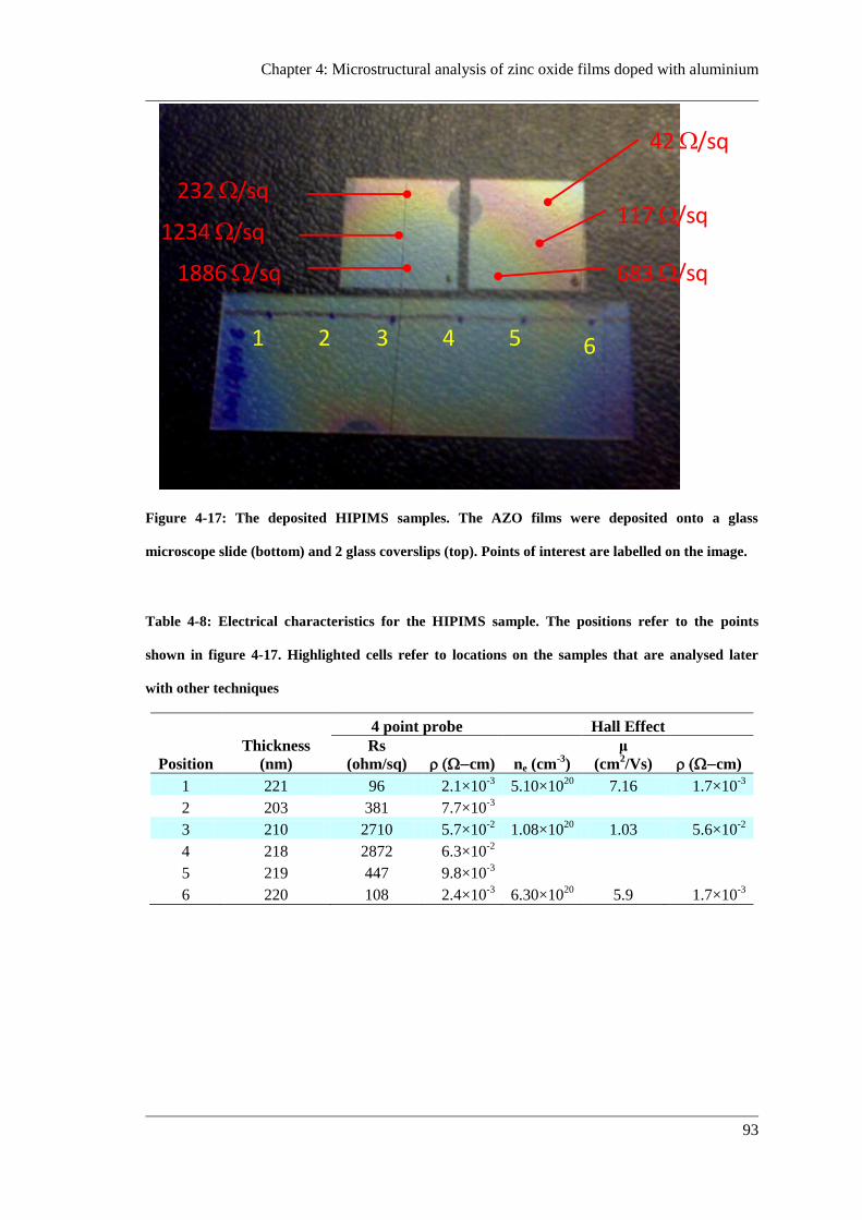
Chapter 4: Microstructural analysis of zinc oxide films doped with aluminium
93
1 2 3 4 5 6
42 /sq
117 /sq
683 /sq
232 /sq
1234 /sq
1886 /sq
Figure 4-17: The deposited HIPIMS samples. The AZO films were deposited onto a glass
microscope slide (bottom) and 2 glass coverslips (top). Points of interest are labelled on the image.
Table 4-8: Electrical characteristics for the HIPIMS sample. The positions refer to the points
shown in figure 4-17. Highlighted cells refer to locations on the samples that are analysed later
with other techniques
4 point probe Hall Effect
Position
Thickness
(nm)
Rs
(ohm/sq) cm) ne (cm-3
)
μ
(cm2/Vs) cm)
1 221 96 2.1×10⁻³
5.10×10²⁰
7.16 1.7×10⁻³
2 203 381 7.7×10⁻³
3 210 2710 5.7×10⁻²
1.08×10²⁰
1.03 5.6×10⁻²
4 218 2872 6.3×10⁻²
5 219 447 9.8×10⁻³
6 220 108 2.4×10⁻³
6.30×10²⁰
5.9 1.7×10⁻³
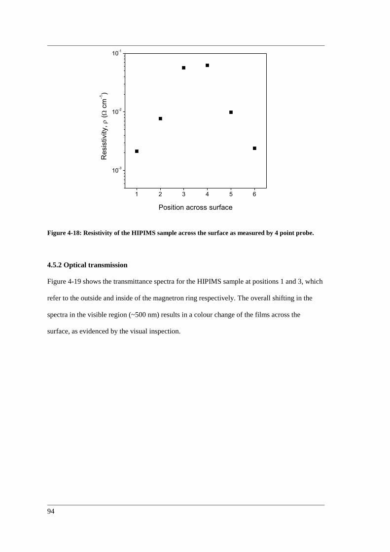
94
1 2 3 4 5 6
10-3
10-2
10-1
Resis
tivity, (
cm
-1)
Position across surface
Figure 4-18: Resistivity of the HIPIMS sample across the surface as measured by 4 point probe.
4.5.2 Optical transmission
Figure 4-19 shows the transmittance spectra for the HIPIMS sample at positions 1 and 3, which
refer to the outside and inside of the magnetron ring respectively. The overall shifting in the
spectra in the visible region (~500 nm) results in a colour change of the films across the
surface, as evidenced by the visual inspection.
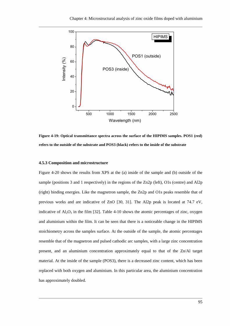
Chapter 4: Microstructural analysis of zinc oxide films doped with aluminium
95
500 1000 1500 2000 2500
0
20
40
60
80
100
POS1 (outside)
Inte
nsity (
%)
Wavelength (nm)
POS3 (inside)
HIPIMS
Figure 4-19: Optical transmittance spectra across the surface of the HIPIMS samples. POS1 (red)
refers to the outside of the substrate and POS3 (black) refers to the inside of the substrate
4.5.3 Composition and microstructure
Figure 4-20 shows the results from XPS at the (a) inside of the sample and (b) outside of the
sample (positions 3 and 1 respectively) in the regions of the Zn2p (left), O1s (centre) and Al2p
(right) binding energies. Like the magnetron sample, the Zn2p and O1s peaks resemble that of
previous works and are indicative of ZnO [30, 31]. The Al2p peak is located at 74.7 eV,
indicative of Al2O3 in the film [32]. Table 4-10 shows the atomic percentages of zinc, oxygen
and aluminium within the film. It can be seen that there is a noticeable change in the HIPIMS
stoichiometry across the samples surface. At the outside of the sample, the atomic percentages
resemble that of the magnetron and pulsed cathodic arc samples, with a large zinc concentration
present, and an aluminium concentration approximately equal to that of the Zn/Al target
material. At the inside of the sample (POS3), there is a decreased zinc content, which has been
replaced with both oxygen and aluminium. In this particular area, the aluminium concentration
has approximately doubled.
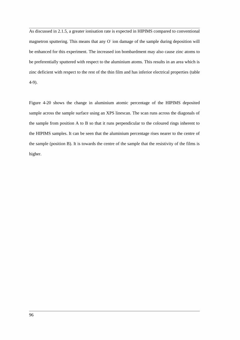
96
As discussed in 2.1.5, a greater ionisation rate is expected in HIPIMS compared to conventional
magnetron sputtering. This means that any O- ion damage of the sample during deposition will
be enhanced for this experiment. The increased ion bombardment may also cause zinc atoms to
be preferentially sputtered with respect to the aluminium atoms. This results in an area which is
zinc deficient with respect to the rest of the thin film and has inferior electrical properties (table
4-9).
Figure 4-20 shows the change in aluminium atomic percentage of the HIPIMS deposited
sample across the sample surface using an XPS linescan. The scan runs across the diagonals of
the sample from position A to B so that it runs perpendicular to the coloured rings inherent to
the HIPIMS samples. It can be seen that the aluminium percentage rises nearer to the centre of
the sample (position B). It is towards the centre of the sample that the resistivity of the films is
higher.
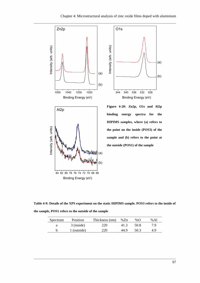
Chapter 4: Microstructural analysis of zinc oxide films doped with aluminium
97
1050 1040 1030 1020
Inte
nsity (
arb
. units)
Binding Energy (eV)
(b)
(a)
Zn2p
544 540 536 532 528
Inte
nsity (
arb
. units)
Binding Energy (eV)
(b)
(a)
O1s
84 82 80 78 76 74 72 70 68 66
Inte
nsity (
arb
. units)
Binding Energy (eV)
(b)
(a)
Al2p
Figure 4-20: Zn2p, O1s and Al2p
binding energy spectra for the
HIPIMS samples, where (a) refers to
the point on the inside (POS3) of the
sample and (b) refers to the point at
the outside (POS1) of the sample
Table 4-9: Details of the XPS experiment on the static HIPIMS sample. POS3 refers to the inside of
the sample, POS1 refers to the outside of the sample
Spectrum Position Thickness (nm) %Zn %O %Al
a 3 (inside) 220 41.3 50.8 7.9
b 1 (outside) 220 44.9 50.3 4.9
98
0 10 20 300
1
2
3
4
5
6
7
8
B
A
% (
Al) w
ith
in s
am
ple
Distance along linescan (mm)
Figure 4-21: XPS line scan of the Al2p peak across the surface of the HIPIMS sample from
position A to B.
Figure 4-22 shows the XRD spectra of the HIPIMS sample at two different positions, one in the
centre of the sample (position 3 from table 4-8) and one towards the outer edge of the sample
(position 1). It can be seen in this case that that both films are disordered with small amounts of
ZnO(002) crystal growth. Due to broadening of the peaks, it is not clear whether the -Al2O3 or
the gahnite phases are present. Between the two positions on the coating, there is a large
variation in the intensity of the ZnO(002) peak, indicating that at the centre of the sample,
significant ion damage to the oriented growth has occurred. This result supports the XPS result
in which it was found that preferential O- ion sputtering of the zinc atoms towards the inside of
the was occurring.
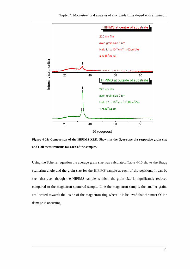
Chapter 4: Microstructural analysis of zinc oxide films doped with aluminium
99
20 40 60 80
20 40 60 80
1
2 (degrees)
220 nm film
aver. grain size 5 nm
Hall: 1.1 x 10²⁰
cm-3, 1.03cm
2/Vs
5.6x10⁻² .cm
Inte
nsity (
arb
. u
nits)
220 nm film
aver. grain size 9 nm
Hall: 5.1 x 10²⁰
cm-3, 7.16cm
2/Vs
1.7x10⁻³ .cm
HIPIMS at centre of substrate
HIPIMS at outside of substrate
1
Figure 4-22: Comparison of the HIPIMS XRD. Shown in the figure are the respective grain size
and Hall measurements for each of the samples.
Using the Scherrer equation the average grain size was calculated. Table 4-10 shows the Bragg
scattering angle and the grain size for the HIPIMS sample at each of the positions. It can be
seen that even though the HIPIMS sample is thick, the grain size is significantly reduced
compared to the magnetron sputtered sample. Like the magnetron sample, the smaller grains
are located towards the inside of the magnetron ring where it is believed that the most O- ion
damage is occurring.
100
Table 4-10: Peak position and grain size analysis of the AZO samples deposited using magnetron
sputtering and HIPIMS.
Sample Thickness (nm) 2B (deg) FWHM (deg) D (nm)
HIPIMS (inside) 220 33.73 1.55 5
HIPIMS (outside) 220 34.10 0.91 9
Figure 4-23a shows the XAS in the region of the aluminium K-edge for HIPIMS deposited
sample at the regions indicated. It can be seen that like the other deposition methods, the peak
at 1567.7 eV shows the presence of octahedrally coordinated Al within the sample, with no
indication of tetrahedrally coordinated Al present. It can be seen from the relative intensities of
the spectra that there is a lot more aluminium present in the HIPIMS sample towards the centre
(as evidenced by the XPS results).. The peaks in the HIPIMS (inside) spectra are also less
resolved than the other spectra, another indication of the disorder present within the film.
Figure 4-23b shows the oxygen K-edge of the HIPIMS samples. Each of the spectra are
characteristic to ZnO. The peak in the HIPIMS (inside) spectra is less well resolved and the
filtered HIPIMS is more resolved, illustrating the change in disorder between the films. Also
shown is the FEFF9 calculation of the ZnO wurtzite phase. Like the magnetron sputtered
samples, a close match is observed.
Figure 4-23c shows the XAS in the region of the zinc L-edges for the HIPIMS samples. These
spectra are characteristic of the Zn L-edge from ZnO [38]. Like the oxygen K-edge, the
crystallographic disorder of the HIPIMS film towards the inside of the sample is reflected in the
XANES with less resolved peaks.
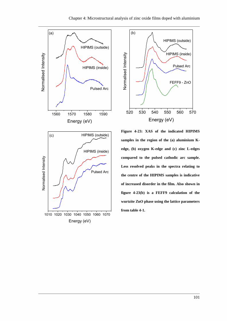
Chapter 4: Microstructural analysis of zinc oxide films doped with aluminium
101
1560 1570 1580 1590
(a)
Pulsed Arc
No
rma
lise
d I
nte
nsity
Energy (eV)
HIPIMS (outside)
HIPIMS (inside)
520 530 540 550 560 570
HIPIMS (inside)
(b)
No
rma
lise
d I
nte
nsity
Energy (eV)
FEFF9 - ZnO
HIPIMS (outside)
Pulsed Arc
1010 1020 1030 1040 1050 1060 1070
(c)
No
rma
lise
d I
nte
nsity
Energy (eV)
HIPIMS (inside)
HIPIMS (outside)
Pulsed Arc
Figure 4-23: XAS of the indicated HIPIMS
samples in the region of the (a) aluminium K-
edge, (b) oxygen K-edge and (c) zinc L-edges
compared to the pulsed cathodic arc sample.
Less resolved peaks in the spectra relating to
the centre of the HIPIMS samples is indicative
of increased disorder in the film. Also shown in
figure 4-23(b) is a FEFF9 calculation of the
wurtzite ZnO phase using the lattice parameters
from table 4-1.
102
4.6 Filtered HIPIMS
The results for the experiments carried out on the filtered HIPIMS deposited samples are
presented in this section. Unlike the magnetron sputtered and HIPIMS samples, visual
inspection of the films showed no noticeable variation in the film structure across the surface,
suggesting that the samples were homogenous.
4.6.1 Resistivity and Hall Effect
Table 4-11 shows the results of the Hall Effect electrical characterisation experiment for the
two films. The immediate effect of the magnetic filter is a higher deposition rate as seen by the
increase in film thickness. This suggests that the filter also acts to better focus Zn and Al ions
generated at the target towards the substrate. More importantly, there is an increase in carrier
concentration (ne), a dramatic increase in the mobility () and a decrease in the resistivity ()
by several orders of magnitude.
Table 4-11: Electrical characteristics for the HIPIMS samples deposited both with and without the
inclusion of the straight magnetic filter.
Deposition
Method
Thickness
(nm) ne (cm-3
) μ (cm2/Vs) cm
-1)
HIPIMS 90 5.8×10²⁰
0.553 1.9×10⁻²
Filtered HIPIMS 180 1.3×10²¹
6.05 7.9×10⁻⁴
4.6.2 Optical transmission
Figure 4-24 shows the transmittance as a function of wavelength for the HIPIMS samples
deposited both with and without the magnetic filter. It can be seen that despite being twice as
thick, the filtered HIPIMS has a higher transmittance in the optical (400-700 nm) region of the
spectrum. This extra thickness of the film has the effect of reducing the transparency in the IR
region (as was seen in the pulsed cathodic arc deposited films).
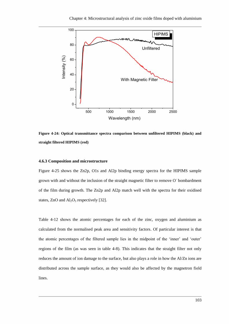
Chapter 4: Microstructural analysis of zinc oxide films doped with aluminium
103
500 1000 1500 2000 2500
0
20
40
60
80
100
HIPIMS
Unfiltered
With Magnetic Filter
Inte
nsity (
%)
Wavelength (nm)
Figure 4-24: Optical transmittance spectra comparison between unfiltered HIPIMS (black) and
straight filtered HIPIMS (red)
4.6.3 Composition and microstructure
Figure 4-25 shows the Zn2p, O1s and Al2p binding energy spectra for the HIPIMS sample
grown with and without the inclusion of the straight magnetic filter to remove O- bombardment
of the film during growth. The Zn2p and Al2p match well with the spectra for their oxidised
states, ZnO and Al2O3 respectively [32].
Table 4-12 shows the atomic percentages for each of the zinc, oxygen and aluminium as
calculated from the normalised peak area and sensitivity factors. Of particular interest is that
the atomic percentages of the filtered sample lies in the midpoint of the ‘inner’ and ‘outer’
regions of the film (as was seen in table 4-8). This indicates that the straight filter not only
reduces the amount of ion damage to the surface, but also plays a role in how the Al/Zn ions are
distributed across the sample surface, as they would also be affected by the magnetron field
lines.
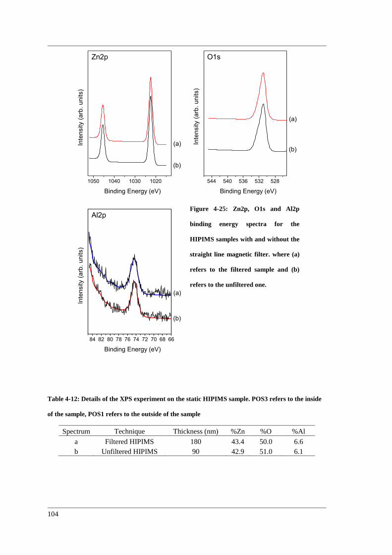
104
1050 1040 1030 1020
Inte
nsity (
arb
. units)
Binding Energy (eV)
(b)
(a)
Zn2p
544 540 536 532 528
Inte
nsity (
arb
. units)
Binding Energy (eV)
(b)
(a)
O1s
84 82 80 78 76 74 72 70 68 66
Inte
nsity (
arb
. units)
Binding Energy (eV)
(b)
(a)
Al2p
Figure 4-25: Zn2p, O1s and Al2p
binding energy spectra for the
HIPIMS samples with and without the
straight line magnetic filter. where (a)
refers to the filtered sample and (b)
refers to the unfiltered one.
Table 4-12: Details of the XPS experiment on the static HIPIMS sample. POS3 refers to the inside
of the sample, POS1 refers to the outside of the sample
Spectrum Technique Thickness (nm) %Zn %O %Al
a Filtered HIPIMS 180 43.4 50.0 6.6
b Unfiltered HIPIMS 90 42.9 51.0 6.1
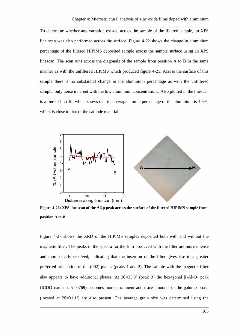
Chapter 4: Microstructural analysis of zinc oxide films doped with aluminium
105
To determine whether any variation existed across the sample of the filtered sample, an XPS
line scan was also performed across the surface. Figure 4-22 shows the change in aluminium
percentage of the filtered HIPIMS deposited sample across the sample surface using an XPS
linescan. The scan runs across the diagonals of the sample from position A to B in the same
manner as with the unfiltered HIPIMS which produced figure 4-21. Across the surface of this
sample there is no substantial change in the aluminium percentage as with the unfiltered
sample, only noise inherent with the low aluminium concentrations. Also plotted in the linescan
is a line of best fit, which shows that the average atomic percentage of the aluminium is 4.8%,
which is close to that of the cathode material.
0 10 20 300
1
2
3
4
5
6
7
8
% (
Al) w
ith
in s
am
ple
Distance along linescan (mm)
BA
Figure 4-26: XPS line scan of the Al2p peak across the surface of the filtered HIPIMS sample from
position A to B.
Figure 4-27 shows the XRD of the HIPIMS samples deposited both with and without the
magnetic filter. The peaks in the spectra for the film produced with the filter are more intense
and more clearly resolved; indicating that the insertion of the filter gives rise to a greater
preferred orientation of the (002) planes (peaks 1 and 2). The sample with the magnetic filter
also appears to have additional phases. At 2=33.0º (peak 3) the hexagonal -Al2O3 peak
(ICDD card no. 51-0769) becomes more prominent and trace amounts of the gahnite phase
(located at 2=31.1º) are also present. The average grain size was determined using the
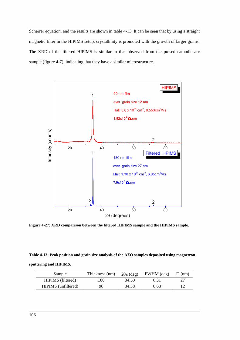
106
Scherrer equation, and the results are shown in table 4-13. It can be seen that by using a straight
magnetic filter in the HIPIMS setup, crystallinity is promoted with the growth of larger grains.
The XRD of the filtered HIPIMS is similar to that observed from the pulsed cathodic arc
sample (figure 4-7), indicating that they have a similar microstructure.
20 40 60 80
20 40 60 80
2
1
180 nm film
aver. grain size 27 nm
Hall: 1.30 x 10²¹
cm-3, 6.05cm
2/Vs
7.9x10⁻⁴ .cm
90 nm film
aver. grain size 12 nm
Hall: 5.8 x 10²⁰
cm-3, 0.553cm
2/Vs
1.92x10⁻² .cm
Filtered HIPIMS
HIPIMS
Inte
nsity (
co
un
ts)
2 (degrees)
23
1
Figure 4-27: XRD comparison between the filtered HIPIMS sample and the HIPIMS sample.
Table 4-13: Peak position and grain size analysis of the AZO samples deposited using magnetron
sputtering and HIPIMS.
Sample Thickness (nm) 2B (deg) FWHM (deg) D (nm)
HIPIMS (filtered) 180 34.50 0.31 27
HIPIMS (unfiltered) 90 34.38 0.68 12
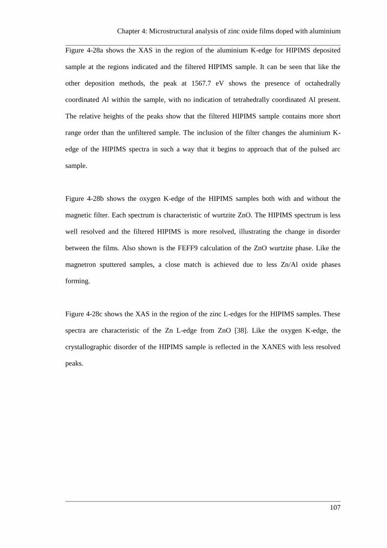
Chapter 4: Microstructural analysis of zinc oxide films doped with aluminium
107
Figure 4-28a shows the XAS in the region of the aluminium K-edge for HIPIMS deposited
sample at the regions indicated and the filtered HIPIMS sample. It can be seen that like the
other deposition methods, the peak at 1567.7 eV shows the presence of octahedrally
coordinated Al within the sample, with no indication of tetrahedrally coordinated Al present.
The relative heights of the peaks show that the filtered HIPIMS sample contains more short
range order than the unfiltered sample. The inclusion of the filter changes the aluminium K-
edge of the HIPIMS spectra in such a way that it begins to approach that of the pulsed arc
sample.
Figure 4-28b shows the oxygen K-edge of the HIPIMS samples both with and without the
magnetic filter. Each spectrum is characteristic of wurtzite ZnO. The HIPIMS spectrum is less
well resolved and the filtered HIPIMS is more resolved, illustrating the change in disorder
between the films. Also shown is the FEFF9 calculation of the ZnO wurtzite phase. Like the
magnetron sputtered samples, a close match is achieved due to less Zn/Al oxide phases
forming.
Figure 4-28c shows the XAS in the region of the zinc L-edges for the HIPIMS samples. These
spectra are characteristic of the Zn L-edge from ZnO [38]. Like the oxygen K-edge, the
crystallographic disorder of the HIPIMS sample is reflected in the XANES with less resolved
peaks.
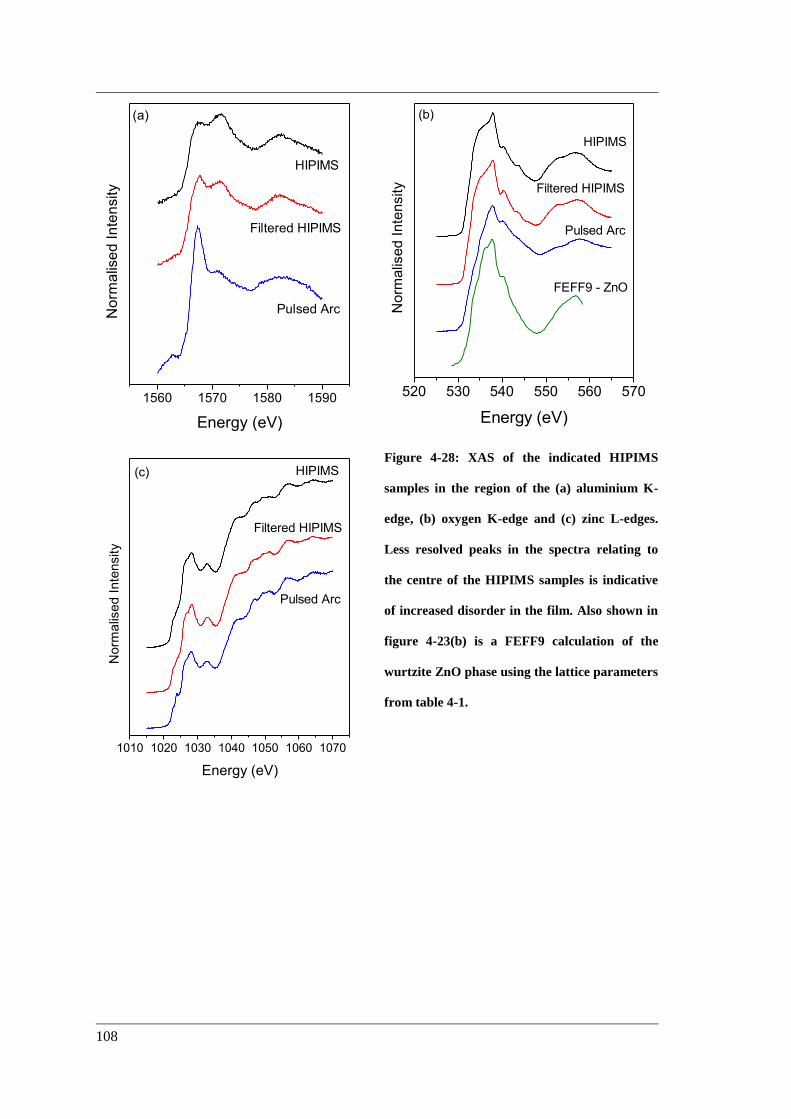
108
1560 1570 1580 1590
(a)
Pulsed Arc
No
rma
lise
d I
nte
nsity
Energy (eV)
HIPIMS
Filtered HIPIMS
520 530 540 550 560 570
Filtered HIPIMS
(b)
No
rma
lise
d I
nte
nsity
Energy (eV)
FEFF9 - ZnO
HIPIMS
Pulsed Arc
1010 1020 1030 1040 1050 1060 1070
(c)
No
rma
lise
d I
nte
nsity
Energy (eV)
Filtered HIPIMS
HIPIMS
Pulsed Arc
Figure 4-28: XAS of the indicated HIPIMS
samples in the region of the (a) aluminium K-
edge, (b) oxygen K-edge and (c) zinc L-edges.
Less resolved peaks in the spectra relating to
the centre of the HIPIMS samples is indicative
of increased disorder in the film. Also shown in
figure 4-23(b) is a FEFF9 calculation of the
wurtzite ZnO phase using the lattice parameters
from table 4-1.
Chapter 4: Microstructural analysis of zinc oxide films doped with aluminium
109
4.7 Comparison of techniques
To get a clearer understanding of the difference between the films deposited using these
techniques, films of a similar thickness were selected and a comparison for each analysis is
made. For the magnetron and HIPIMS coatings, the outer region of the films were selected as
they had the best electrical properties.
Table 4-14 shows a comparison of the electrical properties for each of the films. Figure 4-29
shows a graphical representation of the data in this table. Several can be drawn from this data.
The first is the comparison between the filtered HIPIMS and the unfiltered of similar thickness.
It can be seen that the filtered HIPIMS not only has a lower resistivity (), but also a
significantly higher carrier concentration (ne). As mentioned earlier, it was found that with
increasing thickness, a decrease in and an increase in ne and μ is expected [17, 21, 29]. But
with these results, the thinner filtered sample has lower resistivity, indicating that having the
straight filter within the HIPIMS setup provides better films electrically, probably due to
reduction in O- ion damage to the growing film.
The second point worth noting is that conventional magnetron has the highest resistivity,
approximately double that of the unfiltered HIPIMS sample despite being a much thicker film.
This would indicate that using the high power pulses and the highly ionised plasma in HIPIMS
results in a superior film.
Finally is that the pulsed cathodic arc sample has a much lower resistivity than all of the other
films. The pulsed arc uses a high energy, highly ionised plasma with no macroparticles and few
neutral atoms (both due to 90º filter) to grow thin films. This, along with the observation that
filtered HIPIMS makes for better films than magnetron sputtering further indicates that an
energetic deposition is preferred for making AZO films with low resistivity.
110
Table 4-14: Comparison of electrical properties for each of the listed deposition methods. Films of
similar thickness were chosen so that a fair comparison could be made.
Deposition Method
Thickness
(nm) ne (cm-3
) μ (cm2/Vs) cm
-1)
Pulsed cathodic arc 260 7.63×10²⁰
33.2 2.46×10⁻⁴
Magnetron (POS2) 318 1.56×10²⁰
11.1 3.58×10⁻³
HIPIMS (POS1) 220 5.10×10²⁰
7.16 1.70×10⁻³
Filtered HIPIMS 180 1.30×10²¹
6.05 7.94×10⁻⁴
1018
1019
1020
1021
1022
HIPIMS Magnetron
Re
sis
tivity, (
cm
-1)
Ele
ctr
on
Co
ncen
tra
tio
n,
n (
cm
-3)
Pulsed Arc
10-1
100
101
102
Mo
bili
ty, (
cm
2/V
s)
10-5
10-4
10-3
10-2
Filtered
HIPIMS
n
Figure 4-29: Comparison of the electrical properties for the techniques used to deposit the AZO
films.
Figure 4-30 shows a comparison of the optical transmission between the (a) magnetron
sputtered sample, (b) filtered HIPIMS sample, (c) HIPIMS sample and the (d) pulsed cathodic
arc deposited sample of similar thicknesses. At 550 nm, the region of which the eye is most
sensitive to light, all samples have a similar transparency. Although the magnetron sample is
thicker than the others, it has a higher transmission in both the visible and the infra-red regions
of the spectra than all of the other techniques. This is possibly due to film growth being
primarily from low energy neutrals (<10 eV) in the conventional magnetron. Like the work
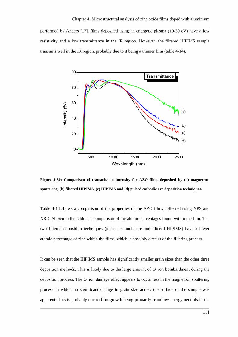
Chapter 4: Microstructural analysis of zinc oxide films doped with aluminium
111
performed by Anders [17], films deposited using an energetic plasma (10-30 eV) have a low
resistivity and a low transmittance in the IR region. However, the filtered HIPIMS sample
transmits well in the IR region, probably due to it being a thinner film (table 4-14).
500 1000 1500 2000 2500
0
20
40
60
80
100
(d)
(c)
(b)
Transmittance
Inte
nsity (
%)
Wavelength (nm)
(a)
Figure 4-30: Comparison of transmission intensity for AZO films deposited by (a) magnetron
sputtering, (b) filtered HIPIMS, (c) HIPIMS and (d) pulsed cathodic arc deposition techniques.
Table 4-14 shows a comparison of the properties of the AZO films collected using XPS and
XRD. Shown in the table is a comparison of the atomic percentages found within the film. The
two filtered deposition techniques (pulsed cathodic arc and filtered HIPIMS) have a lower
atomic percentage of zinc within the films, which is possibly a result of the filtering process.
It can be seen that the HIPIMS sample has significantly smaller grain sizes than the other three
deposition methods. This is likely due to the large amount of O- ion bombardment during the
deposition process. The O- ion damage effect appears to occur less in the magnetron sputtering
process in which no significant change in grain size across the surface of the sample was
apparent. This is probably due to film growth being primarily from low energy neutrals in the
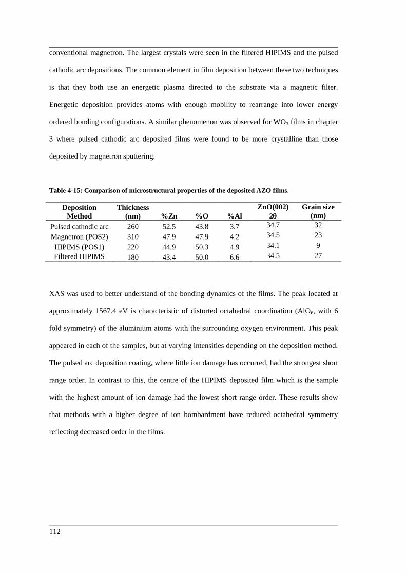
112
conventional magnetron. The largest crystals were seen in the filtered HIPIMS and the pulsed
cathodic arc depositions. The common element in film deposition between these two techniques
is that they both use an energetic plasma directed to the substrate via a magnetic filter.
Energetic deposition provides atoms with enough mobility to rearrange into lower energy
ordered bonding configurations. A similar phenomenon was observed for WO3 films in chapter
3 where pulsed cathodic arc deposited films were found to be more crystalline than those
deposited by magnetron sputtering.
Table 4-15: Comparison of microstructural properties of the deposited AZO films.
Deposition
Method
Thickness
(nm) %Zn %O %Al
ZnO(002)
2
Grain size
(nm)
Pulsed cathodic arc 260 52.5 43.8 3.7 34.7 32
Magnetron (POS2) 310 47.9 47.9 4.2 34.5 23
HIPIMS (POS1) 220 44.9 50.3 4.9 34.1 9
Filtered HIPIMS 180 43.4 50.0 6.6 34.5 27
XAS was used to better understand of the bonding dynamics of the films. The peak located at
approximately 1567.4 eV is characteristic of distorted octahedral coordination (AlO6, with 6
fold symmetry) of the aluminium atoms with the surrounding oxygen environment. This peak
appeared in each of the samples, but at varying intensities depending on the deposition method.
The pulsed arc deposition coating, where little ion damage has occurred, had the strongest short
range order. In contrast to this, the centre of the HIPIMS deposited film which is the sample
with the highest amount of ion damage had the lowest short range order. These results show
that methods with a higher degree of ion bombardment have reduced octahedral symmetry
reflecting decreased order in the films.
Chapter 4: Microstructural analysis of zinc oxide films doped with aluminium
113
4.7 Conclusions
In this chapter, a comparison was made between AZO films prepared using pulsed cathodic arc,
magnetron sputtering and HIPIMS. The pulsed cathodic arc films were found to contain mainly
the wurtzite ZnO phase with the crystals strongly <001> oriented in the direction perpendicular
to the substrate. Also present in the films were a hexagonal aluminium oxide (Al2O3) phase and
traces of the gahnite phase (ZnAl2O4, identified using XRD). This indicates that not all of the
aluminium was substituting into the zinc atom positions. The pulsed arc samples were found to
have good electrical properties, with low resistivities and high carrier concentrations even for
quite thin films. The films displayed favourable optical properties, with transmissions of
approximately 85% found in the visible region.
On visual inspection of the magnetron sputtered films, there appeared to be variations in the
colour across the surface. Even though the microstructure of the films did not appear to change
across the surface, the electrical and optical properties changed dramatically. In particular, the
area of the film in line with the centre of the magnetron was found to have inferior resistivities,
orders of magnitude higher than the outside of the film. These results indicate the presence of
O- ions bombarding the films during reactive deposition which had a major impact on the
electrical and optical properties. The increase in power inherent with the HIPIMS process was
found to exacerbate the problem of ion bombardment with large variations in the optical and
electrical properties found across the surface of films prepared using this technique. Unlike
magnetron sputtering, the change in film across the surface was also reflected in the
microstructure with x-ray analysis revealing a significant reduction in crystallinity and
composition in line with the centre of the magnetron.
The inclusion of a magnetic filter between the magnetron and the sample had the effect of
removing the majority of the damaging ions, allowing for a more crystalline film to grow with
114
enhanced optical and electrical properties. The use of such filters may therefore help overcome
one of the major disadvantages of the HIPIMS techniques which has been low deposition rates.
The microstructure of the film prepared using the filter was found to be similar to that deposited
using the pulsed cathodic arc. These results suggest that the optimal conditions for AZO film
growth are with energetic ions which provide mobility to the deposited atoms allowing them to
rearrange into more ordered arrangements. The use of the straight filter also had the side benefit
of increasing the HIPIMS deposition rate by better directing the Zn and Al ions from the target
towards the substrate.
4.8 Bibliography
1. Minami, T., Present status of transparent conducting oxide thin-film development for
Indium-Tin-Oxide (ITO) substitutes. Thin Solid Films, 2008. 516(17): p. 5822-5828.
2. Harrison, S.E., Conductivity and Hall Effect of ZnO at Low Temperatures. Physical
Review, 1954. 93(1): p. 52.
3. Mohanty, G.P. and L.V. Azaroff, Electron Density Distributions in ZnO Crystals. The
Journal of Chemical Physics, 1961. 35(4): p. 1268-1270.
4. Ritchie, I.M. and R.K. Tandon, Some doping studies on the oxidation of zinc in the
temperature range 200-390°C. Surface Science, 1970. 22(1): p. 199-215.
5. McKeown, D.A., Aluminum X-ray absorption near-edge spectra of some oxide
minerals: Calculation versus experimental data. Physics and Chemistry of Minerals,
1989. 16(7): p. 678-683.
6. Karzel, H., W. Potzel, ouml, M. fferlein, W. Schiessl, M. Steiner, U. Hiller, G.M.
Kalvius, D.W. Mitchell, T.P. Das, P. Blaha, K. Schwarz, and M.P. Pasternak, Lattice
dynamics and hyperfine interactions in ZnO and ZnSe at high external pressures.
Physical Review B, 1996. 53(17): p. 11425.
7. Minami, T., T. Yamamoto, and T. Miyata, Highly transparent and conductive rare
earth-doped ZnO thin films prepared by magnetron sputtering. Thin Solid Films, 2000.
366(1-2): p. 63-68.
8. Thu, T.V. and S. Maenosono, Synthesis of high-quality Al-doped ZnO nanoink. Journal
of Applied Physics, 2010. 107(1): p. 014308-6.
9. Ashrafi, A.B.M.A., A. Ueta, A. Avramescu, H. Kumano, I. Suemune, Y.-W. Ok, and
T.-Y. Seong, Growth and characterization of hypothetical zinc-blende ZnO films on
GaAs(001) substrates with ZnS buffer layers. Applied Physics Letters, 2000. 76(5): p.
550-552.
10. Ozgur, U., Y.I. Alivov, C. Liu, A. Teke, M.A. Reshchikov, S. Dogan, V. Avrutin, S.-J.
Cho, and H. Morkoc, A comprehensive review of ZnO materials and devices. Journal of
Applied Physics, 2005. 98(4): p. 041301.
11. Look, D.C., R.L. Jones, J.R. Sizelove, N.Y. Garces, N.C. Giles, and L.E. Halliburton,
The path to ZnO devices: donor and acceptor dynamics. physica status solidi (a), 2003.
195(1): p. 171-177.
12. Park, C.H., S.B. Zhang, and S.-H. Wei, Origin of p-type doping difficulty in ZnO: The
impurity perspective. Physical Review B, 2002. 66(7): p. 073202.
13. Tsujino, J., N. Homma, T. Sugawara, I. Shimono, and Y. Abe, Preparation of Al-doped
ZnO thin films by RF thermal plasma evaporation. Thin Solid Films, 2002. 407(1-2): p.
86-91.
Chapter 4: Microstructural analysis of zinc oxide films doped with aluminium
115
14. Miyazaki, M., K. Sato, A. Mitsui, and H. Nishimura, Properties of Ga-doped ZnO
films. Journal of Non-Crystalline Solids, 1997. 218: p. 323-328.
15. Shinde, S.S. and et al., Optoelectronic properties of sprayed transparent and
conducting indium doped zinc oxide thin films. Journal of Physics D: Applied Physics,
2008. 41(10): p. 105109.
16. Rousset, J., E. Saucedo, and D. Lincot, Extrinsic Doping of Electrodeposited Zinc
Oxide Films by Chlorine for Transparent Conductive Oxide Applications. Chemistry of
Materials, 2009. 21(3): p. 534-540.
17. Anders, A., S.H.N. Lim, K.M. Yu, J. Andersson, J. Rosén, M. McFarland, and J.
Brown, High quality ZnO:Al transparent conducting oxide films synthesized by pulsed
filtered cathodic arc deposition. Thin Solid Films, 2010. 518(12): p. 3313-3319.
18. Lim, D.G., D.H. Kim, J.K. Kim, O. Kwon, K.J. Yang, K.I. Park, B.S. Kim, S.W. Lee,
M.W. Park, and D.J. Kwak, Improved electrical properties of ZnO:Al transparent
conducting oxide films using a substrate bias. Superlattices and Microstructures, 2006.
39(1-4): p. 107-114.
19. Lin, S.-S., J.-L. Huang, and P. Sajgalik, The properties of heavily Al-doped ZnO films
before and after annealing in the different atmosphere. Surface and Coatings
Technology, 2004. 185(2-3): p. 254-263.
20. Lu, J.G., Z.Z. Ye, Y.J. Zeng, L.P. Zhu, L. Wang, J. Yuan, B.H. Zhao, and Q.L. Liang,
Structural, optical, and electrical properties of (Zn,Al)O films over a wide range of
compositions. Journal of Applied Physics, 2006. 100(7): p. 073714-11.
21. Schuler, T. and M.A. Aegerter, Optical, electrical and structural properties of sol gel
ZnO:Al coatings. Thin Solid Films, 1999. 351(1-2): p. 125-131.
22. Murdoch, G.B., S. Hinds, E.H. Sargent, S.W. Tsang, L. Mordoukhovski, and Z.H. Lu,
Aluminum doped zinc oxide for organic photovoltaics. Applied Physics Letters, 2009.
94(21): p. 213301-3.
23. Saarenpää, H., T. Niemi, A. Tukiainen, H. Lemmetyinen, and N. Tkachenko,
Aluminum doped zinc oxide films grown by atomic layer deposition for organic
photovoltaic devices. Solar Energy Materials and Solar Cells, 2010. 94(8): p. 1379-
1383.
24. Xu, J., H. Wang, L. Yang, M. Jiang, S. Wei, and T. Zhang, Low temperature growth of
highly crystallized ZnO:Al films by ultrasonic spray pyrolysis from acetylacetone salt.
Materials Science and Engineering: B, 2010. 167(3): p. 182-186.
25. Mraz, S. and J.M. Schneider, Energy distribution of O- ions during reactive magnetron
sputtering. Applied Physics Letters, 2006. 89(5): p. 051502-3.
26. Bilek, M.M.M., M.M.M. Bilek, R.N. Tarrant, D.R. McKenzie, S.H.N.A.L.S.H.N. Lim,
and D.G.A.M.D.G. McCulloch, Control of stress and microstructure in cathodic arc
deposited films. Plasma Science, IEEE Transactions on, 2003. 31(5): p. 939-944.
27. Brown, I.G., Cathodic arc deposition of films. Annual Review of Materials Science,
1998. 28(1): p. 243-269.
28. Anders, A., R.A. MacGill, and T.A. McVeigh, Efficient, compact power supply for
repetitively pulsed, ``triggerless'' cathodic arcs. Review of Scientific Instruments,
1999. 70(12): p. 4532-4535.
29. Tseng, Y.-K., G.-J. Gao, and S.-C. Chien, Synthesis of c-axis preferred orientation
ZnO:Al transparent conductive thin films using a novel solvent method. Thin Solid
Films, 2010. 518(22): p. 6259-6263.
30. Hullavarad, S., N. Hullavarad, D. Look, and B. Claflin, Persistent Photoconductivity
Studies in Nanostructured ZnO UV Sensors. Nanoscale Research Letters, 2009. 4(12):
p. 1421-1427.
31. Mar, L.G., P.Y. Timbrell, and R.N. Lamb, An XPS study of zinc oxide thin film growth
on copper using zinc acetate as a precursor. Thin Solid Films, 1993. 223(2): p. 341-
347.
32. Scofield, J.H., Hartree-Slater subshell photoionization cross-sections at 1254 and 1487
eV. Journal of Electron Spectroscopy and Related Phenomena, 1976. 8(2): p. 129-137.
116
33. Labidi, A., C. Jacolin, M. Bendahan, A. Abdelghani, J. Guérin, K. Aguir, and M.
Maaref, Impedance spectroscopy on WO3 gas sensor. Sensors and Actuators B:
Chemical, 2005. 106(2): p. 713-718.
34. Dasgupta, N.P., S. Neubert, W. Lee, O. Trejo, J.-R. Lee, and F.B. Prinz, Atomic Layer
Deposition of Al-doped ZnO Films: Effect of Grain Orientation on Conductivity.
Chemistry of Materials, 2010. 22(16): p. 4769-4775.
35. Fang, G. and et al., Magnetron sputtered AZO thin films on commercial ITO glass for
application of a very low resistance transparent electrode. Journal of Physics D:
Applied Physics, 2002. 35(23): p. 3096.
36. Ildefonse, P., D. Cabaret, P. Sainctavit, G. Calas, A.M. Flank, and P. Lagarde,
Aluminium X-ray absorption Near Edge Structure in model compounds and Earth’s
surface minerals. Physics and Chemistry of Minerals, 1998. 25(2): p. 112-121.
37. Chen, J.G., NEXAFS investigations of transition metal oxides, nitrides, carbides,
sulfides and other interstitial compounds. Surface Science Reports, 1997. 30(1-3): p. 1-
152.
38. Mizoguchi, T., I. Tanaka, S. Yoshioka, M. Kunisu, T. Yamamoto, and W.Y. Ching,
First-principles calculations of ELNES and XANES of selected wide-gap materials:
Dependence on crystal structure and orientation. Physical Review B, 2004. 70(4): p.
045103.
39. Stadelmann, P., JEMS Java Electron Microscopy Software, Available from:
http://cimewww.epfl.ch/people/stadelmann/jemsWebSite/jems.html.
Chapter 5: The microstructure and electrical properties of hafnium oxide
117
Chapter 5
The microstructure and electrical properties
of hafnium oxide prepared using filtered cathodic vacuum arc
In this chapter hafnium oxide (HfO2) films were deposited with a range of substrate biases and
substrate temperatures using a filtered cathodic vacuum arc (FCVA) deposition system. The
microstructure, electronic structure and electrical breakdown of the films were characterised.
Diffraction and the near edge structure (NES) measurements of the oxygen K-edge were used to
determine the phase present. The goal was to determine the optimal growth conditions to
produce HfO2 films with the best electrical breakdown characteristics.
118
5.1 Introduction
5.1.1 Hafnium oxide as a dielectric
The drive to decrease feature sizes in microelectronics has led to the gate oxide thickness in
silicon devices approaching its fundamental limit [1, 2]. Silicon dioxide (SiO2) has been used as
the gate material in transistors for decades and is constantly being made thinner to improve
performance by increasing the gate capacitance [3, 4]. However with decreasing SiO2 size,
undesirable leakage current due to tunnelling through the device is increased, compromising
device performance by increasing power consumption and reducing reliability. Replacing SiO2
with a material with a higher dielectric constant (for example HfO2, ZrO2 or TiO2) has potential
to increase the gate capacitance with decreased thickness and significantly reduced leakage
currents [2].
Hafnium oxide (HfO2) is a particularly promising replacement for SiO2 due to its high dielectric
constant, wide bandgap and low leakage characteristics [5, 6]. Figure 5-1 shows a schematic of
HfO2 acting as a gate dielectric between the gate which has a potential applied to it and a field
effect transistor substrate (silicon in this case). When a large enough potential is supplied
between the gate (HfO2) and body (Si) terminals, a ‘channel’, also known as an inversion layer,
forms between the dielectric material and the body. This channel provides a current path
between source and the drain electrodes which can be switched on/off using the potential
applied to the gate. The ‘source’ is the aptly named source of the charge carriers which pass
through the channel and exit via the ‘drain’. These regions can either be p-type or n-type, but
must be the opposite type to the body region (silicon can be doped to choose a particular type).
In the case of a p-type MOS, the source is a ‘p+’ region and contains electron holes, in the case
of an n-type MOS the source is an ‘n+’ region and supplies electrons for the channel.
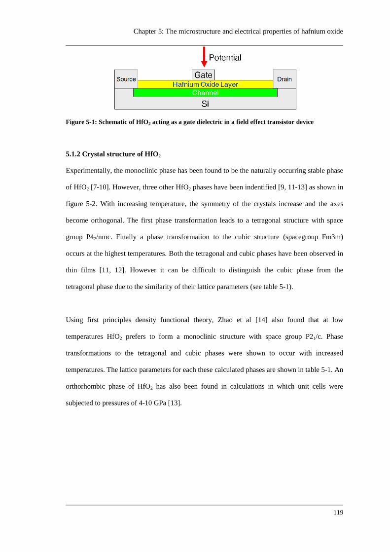
Chapter 5: The microstructure and electrical properties of hafnium oxide
119
Figure 5-1: Schematic of HfO2 acting as a gate dielectric in a field effect transistor device
5.1.2 Crystal structure of HfO2
Experimentally, the monoclinic phase has been found to be the naturally occurring stable phase
of HfO2 [7-10]. However, three other HfO2 phases have been indentified [9, 11-13] as shown in
figure 5-2. With increasing temperature, the symmetry of the crystals increase and the axes
become orthogonal. The first phase transformation leads to a tetragonal structure with space
group P42/nmc. Finally a phase transformation to the cubic structure (spacegroup Fm3m)
occurs at the highest temperatures. Both the tetragonal and cubic phases have been observed in
thin films [11, 12]. However it can be difficult to distinguish the cubic phase from the
tetragonal phase due to the similarity of their lattice parameters (see table 5-1).
Using first principles density functional theory, Zhao et al [14] also found that at low
temperatures HfO2 prefers to form a monoclinic structure with space group P21/c. Phase
transformations to the tetragonal and cubic phases were shown to occur with increased
temperatures. The lattice parameters for each these calculated phases are shown in table 5-1. An
orthorhombic phase of HfO2 has also been found in calculations in which unit cells were
subjected to pressures of 4-10 GPa [13].
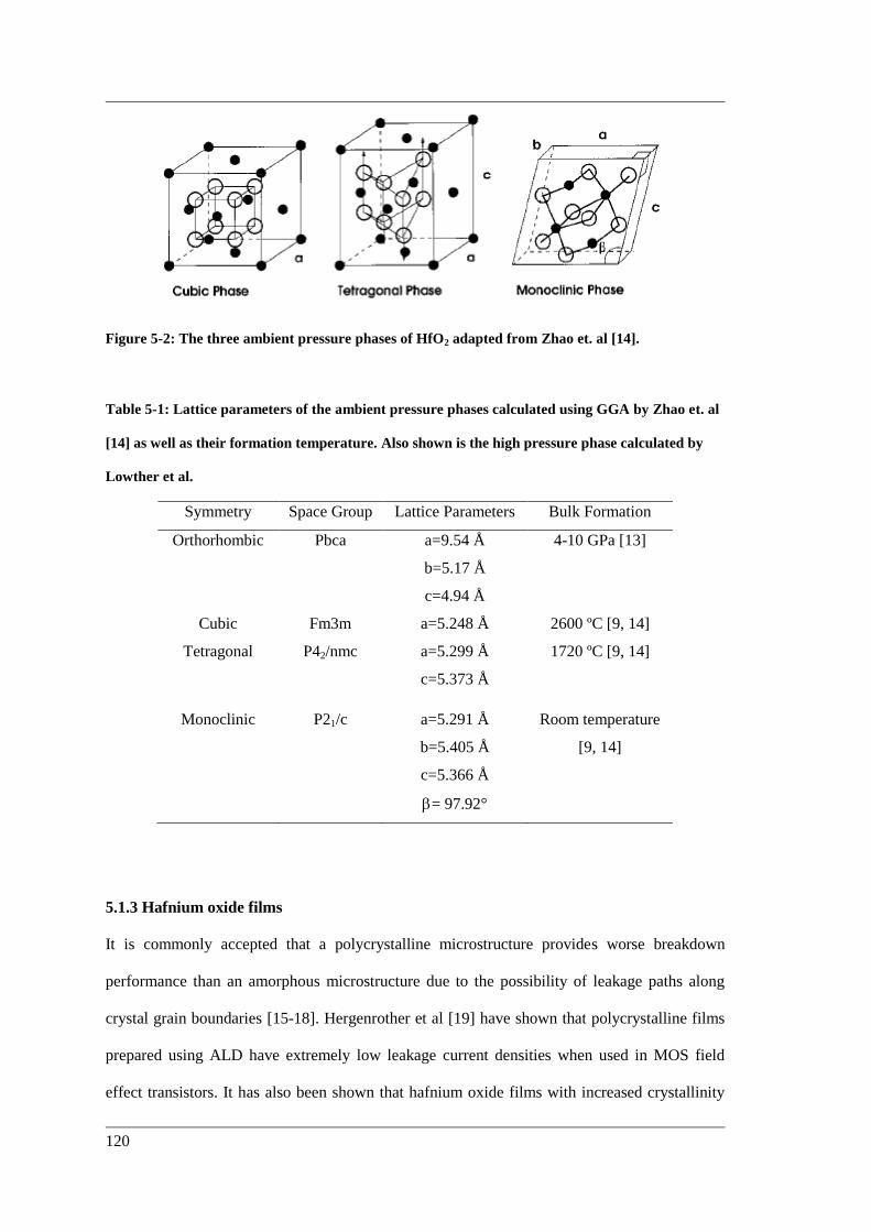
120
Figure 5-2: The three ambient pressure phases of HfO2 adapted from Zhao et. al [14].
Table 5-1: Lattice parameters of the ambient pressure phases calculated using GGA by Zhao et. al
[14] as well as their formation temperature. Also shown is the high pressure phase calculated by
Lowther et al.
Symmetry Space Group Lattice Parameters Bulk Formation
Orthorhombic Pbca a=9.54 Å
b=5.17 Å
c=4.94 Å
4-10 GPa [13]
Cubic Fm3m a=5.248 Å 2600 ºC [9, 14]
Tetragonal P42/nmc a=5.299 Å
c=5.373 Å
1720 ºC [9, 14]
Monoclinic P21/c a=5.291 Å
b=5.405 Å
c=5.366 Å
= 97.92°
Room temperature
[9, 14]
5.1.3 Hafnium oxide films
It is commonly accepted that a polycrystalline microstructure provides worse breakdown
performance than an amorphous microstructure due to the possibility of leakage paths along
crystal grain boundaries [15-18]. Hergenrother et al [19] have shown that polycrystalline films
prepared using ALD have extremely low leakage current densities when used in MOS field
effect transistors. It has also been shown that hafnium oxide films with increased crystallinity
Chapter 5: The microstructure and electrical properties of hafnium oxide
121
have higher dielectric constants [15]. It is therefore important to understand, for a particular
synthesis technique, the relationship between the deposition conditions on the microstructure
and the breakdown characteristics of the HfO2 thin films.
Ho et al [20] found that polycrystalline films prepared by atomic layer deposition (ALD) with
large uniform grain size may be preferable. It is suggested that this will help minimise the
variations in the effective electric field experienced by carriers in the underlying channel. XRD
was performed to determine the phase of the crystals deposited using ALD and to determine the
average crystal size. It is found that with increasing deposition temperature that the intensity of
the monoclinic peaks increases, while the peaks of other unknown phases disappear. It was
noted that more work was necessary to determine whether the other phases are tetragonal or
orthorhombic. This study could potentially have used a combination of ab initio calculations
and a study of the near edge structure to differentiate between the phases.
Techniques which can produce dense flat HfO2 films with fine grain structure are desirable.
With these properties in mind, ALD [21], pulsed laser deposition (PLD) [22, 23], chemical
vapour deposition (CVD) [24] and electron beam evaporation [25] have all been employed to
produce HfO2 films.
In the work by Ratzke et al [22] PLD was used to deposit HfO2 films. PLD produces a similar
energetic plasma to cathodic arc, by using a laser to produce an explosive emission of ions and
neutrals from the surface of the cathode material. Ratzke found that during deposition, what
appeared to be large macroparticle ‘splashes’ were forming on the surface of the sample. The
diameter of the splashes appeared to be dependent on the wavelength of the laser with average
size of 0.6 m, 0.7 m and 1.0 m for wavelengths of 355 nm, 532 nm and 1064 nm
respectively. A similar study was later performed by Filipescu [26] who also deposited hafnium
oxide films using PLD. A more thorough investigation was performed with both the
122
microstructure and the electrical breakdown studied. The HfO2 films displayed low leakage
currents, had an amorphous microstructure and was both smooth and uniform.
Despite all the work preformed to date, it still remains a challenge to produce low leakage
hafnium oxide coatings on silicon without interfacial layers, particularly SiO2, which tend to
form at the metal-oxide/silicon interface [5, 27]. Little work has been done on the synthesis of
HfO2 films by FCVA despite the fact that the technique has been shown to produce dense flat
films with easily controllable thickness [28, 29].
In this chapter, HfO2 thin films are deposited using an FCVA. It has already been shown that
varying the temperature or substrate bias during deposition can alter the microstructure and
physical properties of films prepared by FCVA deposition [28, 29]. Given that changes in
crystallinity may alter the leakage current through the films, the effect of substrate temperature
and bias are investigated. The microstructure and electronic structure of the films are studied to
investigate which films give the best electrical breakdown (leakage) characteristics.
5.2 Experimental techniques
All hafnium oxide films were deposited onto p-type <100> silicon substrates ( < 10 cm)
which were cleaned using acetone and ethanol prior to insertion into the system. Details of the
FCVA system used for the depositions can be found in section 2.1.2. A 99.9 % purity, 70 mm
diameter hafnium metal cathode source was operated with an arc current of 140 A. Oxygen gas
was bled directly into the chamber and the flow rate was controlled using a mass flow
controller (MFC). A second MFC was used to control the flow of argon gas into the cathode
chamber in order to stabilise the plasma and reduce oxidation of the cathode [30]. The system
was pumped to a base pressure of less than 1 10-5
Torr before each deposition. A constant
flow of argon gas (5 ml/min) and oxygen gas (20 ml/min) was utilised during the 2 minute long
deposition, each with partial pressures of 0.21 mTorr and 0.75 mTorr respectively. This gas mix
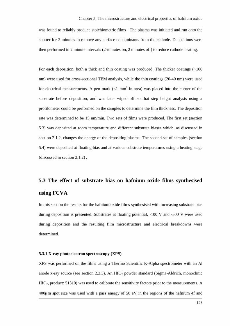
Chapter 5: The microstructure and electrical properties of hafnium oxide
123
was found to reliably produce stoichiometric films . The plasma was initiated and run onto the
shutter for 2 minutes to remove any surface contaminants from the cathode. Depositions were
then performed in 2 minute intervals (2-minutes on, 2 minutes off) to reduce cathode heating.
For each deposition, both a thick and thin coating was produced. The thicker coatings (~100
nm) were used for cross-sectional TEM analysis, while the thin coatings (20-40 nm) were used
for electrical measurements. A pen mark (<1 mm2 in area) was placed into the corner of the
substrate before deposition, and was later wiped off so that step height analysis using a
profilometer could be performed on the samples to determine the film thickness. The deposition
rate was determined to be 15 nm/min. Two sets of films were produced. The first set (section
5.3) was deposited at room temperature and different substrate biases which, as discussed in
section 2.1.2, changes the energy of the depositing plasma. The second set of samples (section
5.4) were deposited at floating bias and at various substrate temperatures using a heating stage
(discussed in section 2.1.2) .
5.3 The effect of substrate bias on hafnium oxide films synthesised
using FCVA
In this section the results for the hafnium oxide films synthesised with increasing substrate bias
during deposition is presented. Substrates at floating potential, -100 V and -500 V were used
during deposition and the resulting film microstructure and electrical breakdowns were
determined.
5.3.1 X-ray photoelectron spectroscopy (XPS)
XPS was performed on the films using a Thermo Scientific K-Alpha spectrometer with an Al
anode x-ray source (see section 2.2.3). An HfO2 powder standard (Sigma-Aldrich, monoclinic
HfO2, product: 51310) was used to calibrate the sensitivity factors prior to the measurements. A
400m spot size was used with a pass energy of 50 eV in the regions of the hafnium 4f and

124
oxygen 1s binding energy spectra. Figures 5-3 and 5-4 show the Hf4f and O1s XPS spectra for
the indicated substrate biases. The Hf4f spectra are made up of a doublet, comprised of the 4f7
and 4f5 peaks at 17.2 eV and 18.6 eV respectively, typical of a single HfO2 species [31]. Small
changes in these peak positions are attributed to sample charging during the XPS experiment.
The O1s spectra is made up of a combination of two peaks. The first is located at approximately
530 eV and is representative of the oxygen bonded to hafnium in the form of HfO2 [32, 33].
The second peak is located at 532 eV and is due to surface oxygen/carbon remaining on the
surface after the sputter clean [34]. Table 5-2 shows the atomic percentages of the films
calculated using the normalised peak area and the film thicknesses. Each of the films is close to
stoichiometric HfO2.
24 22 20 18 16 14 12 10
Inte
nsity (
arb
. u
nits)
Binding Energy (eV)
Floating
-100 V
-500 V
Figure 5-3: XPS spectra of the HfO2 films with the indicated substrate biases in the region of the
hafnium 4f binding energy peaks.
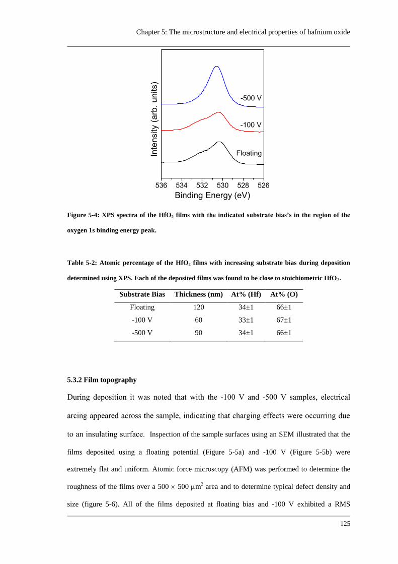
Chapter 5: The microstructure and electrical properties of hafnium oxide
125
536 534 532 530 528 526
Inte
nsity (
arb
. u
nits)
Binding Energy (eV)
Floating
-100 V
-500 V
Figure 5-4: XPS spectra of the HfO2 films with the indicated substrate bias’s in the region of the
oxygen 1s binding energy peak.
Table 5-2: Atomic percentage of the HfO2 films with increasing substrate bias during deposition
determined using XPS. Each of the deposited films was found to be close to stoichiometric HfO2.
Substrate Bias Thickness (nm) At% (Hf) At% (O)
Floating 120 34±1 66±1
-100 V 60 33±1 67±1
-500 V 90 34±1 66±1
5.3.2 Film topography
During deposition it was noted that with the -100 V and -500 V samples, electrical
arcing appeared across the sample, indicating that charging effects were occurring due
to an insulating surface. Inspection of the sample surfaces using an SEM illustrated that the
films deposited using a floating potential (Figure 5-5a) and -100 V (Figure 5-5b) were
extremely flat and uniform. Atomic force microscopy (AFM) was performed to determine the
roughness of the films over a 500 500 m2 area and to determine typical defect density and
size (figure 5-6). All of the films deposited at floating bias and -100 V exhibited a RMS
126
roughness of less than 2 % of the total deposited film thickness. Defects with a large range of
feature sizes appeared in the sample deposited with -500 V bias. Craters up to approximately
100 m in diameter were observed in the SEM images (Figure 5-5c).
At higher resolutions small pin-holes of the order of 10 nm in diameter were revealed (Figure
5-6c). The craters can be attributed to charging/discharging of the substrate during film
deposition, the effects of which (electrical arcing across the sample surface) were observed
during deposition through a window. Energy dispersive spectroscopy revealed that the craters
in the films were composed mostly of the silicon substrate. It is believed that with high negative
substrate bias, the electric field across the film increases during deposition until local
breakdown occurs causing damage to the film and underlying silicon. The pin-holes probably
arise either from smaller breakdown events or densification of the film during growth and were
only found in the film deposited at -500 V substrate bias.
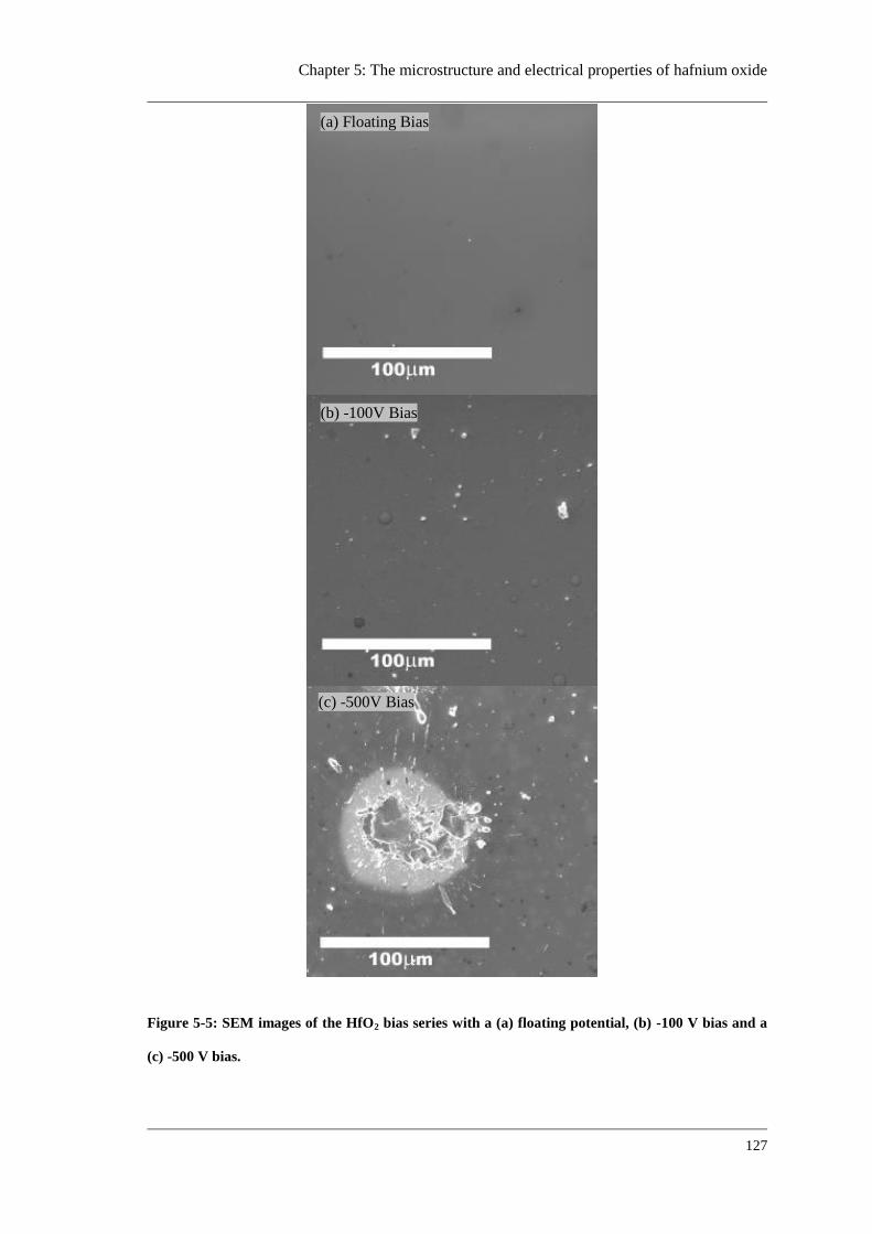
Chapter 5: The microstructure and electrical properties of hafnium oxide
127
Figure 5-5: SEM images of the HfO2 bias series with a (a) floating potential, (b) -100 V bias and a
(c) -500 V bias.
(a) Floating Bias
(b) -100V Bias
(c) -500V Bias
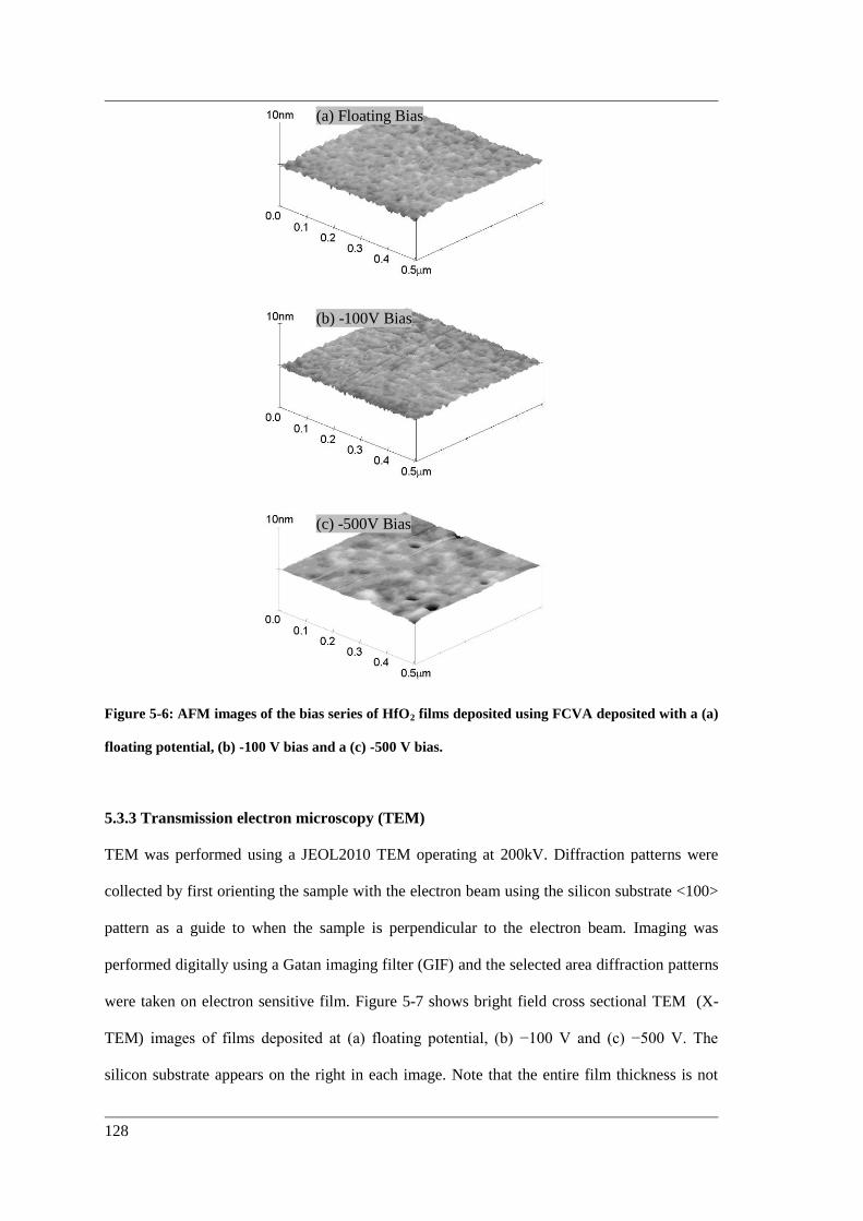
128
Figure 5-6: AFM images of the bias series of HfO2 films deposited using FCVA deposited with a (a)
floating potential, (b) -100 V bias and a (c) -500 V bias.
5.3.3 Transmission electron microscopy (TEM)
TEM was performed using a JEOL2010 TEM operating at 200kV. Diffraction patterns were
collected by first orienting the sample with the electron beam using the silicon substrate <100>
pattern as a guide to when the sample is perpendicular to the electron beam. Imaging was
performed digitally using a Gatan imaging filter (GIF) and the selected area diffraction patterns
were taken on electron sensitive film. Figure 5-7 shows bright field cross sectional TEM (X-
TEM) images of films deposited at (a) floating potential, (b) −100 V and (c) −500 V. The
silicon substrate appears on the right in each image. Note that the entire film thickness is not
(a) Floating Bias
(b) -100V Bias
(c) -500V Bias
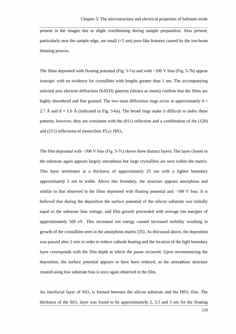
Chapter 5: The microstructure and electrical properties of hafnium oxide
129
present in the images due to slight overthinning during sample preparation. Also present,
particularly near the sample edge, are small (<5 nm) pore-like features caused by the ion-beam
thinning process.
The films deposited with floating potential (Fig. 5-7a) and with −100 V bias (Fig. 5-7b) appear
isotropic with no evidence for crystallites with lengths greater than 1 nm. The accompanying
selected area electron diffraction (SAED) patterns (shown as insets) confirm that the films are
highly disordered and fine grained. The two main diffraction rings occur at approximately d =
2.7 Å and d = 1.6 Å (indicated in Fig. 5-6a). The broad rings make it difficult to index these
patterns, however, they are consistent with the (011) reflection and a combination of the (120)
and (211) reflections of monoclinic P21/c HfO2.
The film deposited with −500 V bias (Fig. 5-7c) shows three distinct layers. The layer closest to
the substrate again appears largely amorphous but large crystallites are seen within the matrix.
This layer terminates at a thickness of approximately 25 nm with a lighter boundary
approximately 2 nm in width. Above this boundary, the structure appears amorphous and
similar to that observed in the films deposited with floating potential and −100 V bias. It is
believed that during the deposition the surface potential of the silicon substrate was initially
equal to the substrate bias voltage, and film growth proceeded with average ion energies of
approximately 500 eV. This increased ion energy caused increased mobility resulting in
growth of the crystallites seen in the amorphous matrix [35]. As discussed above, the deposition
was paused after 2 min in order to reduce cathode heating and the location of the light boundary
layer corresponds with the film depth at which the pause occurred. Upon recommencing the
deposition, the surface potential appears to have been reduced, as the amorphous structure
created using low substrate bias is once again observed in the film.
An interfacial layer of SiO2 is formed between the silicon substrate and the HfO2 film. The
thickness of the SiO2 layer was found to be approximately 2, 3.5 and 5 nm for the floating
130
sample, −100 V bias sample and −500 V biased sample, respectively. This thickness variation
in the native oxide can be attributed to oxygen bombardment during the initial stages of film
growth, with implantation depths that increase with the applied substrate bias.
Figure 5-7: Bright field cross-sectional TEM images of the (a) sample deposited at floating
potential, (b) −100 V bias sample and the (c) −500 V bias sample. Note that the diffraction pattern
in (c) contains diffraction spots from the [011] zone axis of the Si substrate. The two main
diffraction rings indicated in (a) occur at d = 2.7 Å and d = 1.6 Å and can be indexed to the (011)
and a combination of the (120) and (211) reflections of monoclinic P21/c HfO2.
(a) Floating Bias
(b) -100V Bias
(c) -500V Bias
Chapter 5: The microstructure and electrical properties of hafnium oxide
131
5.3.4 Electron energy loss spectroscopy (EELS)
EELS was performed on the HfO2 films using the GIF spectrometer in the TEM with an
entrance aperture of 2 mm. The FWHM of the zero loss peak was measured to be
approximately 2 eV. The region in the vicinity of the oxygen k-edge was scanned and the
background removed.
In 2004, an in depth study by McComb et al [1] was performed on a range of hafnium oxide
related crystalline standards using EELS. Of specific interest was the near edge structure
comparison between experimentally collected monoclinic HfO2 and the same structure
calculated using the FEFF8 code. A very close match of peak position and relative heights
between experiment and calculation was found. In a similar way, the oxygen k-edge of the
HfO2 films deposited in this study at floating and -500 V potentials were compared to a FEFF8
calculation of the monoclinic structure (figure 5-8). Broadening was added to the calculation to
account for instrumental and lifetime broadening in the EELS experiment. It can be seen that
the main peak in the floating potential sample is less resolved than that in the biased sample,
indicating that more disorder is present within the film. The peak positions and relative heights
compare well with that found in previous results [1, 36], but the main peaks are not as well
resolved. This could either be a result of increased disorder in the films or instrumental
broadening.
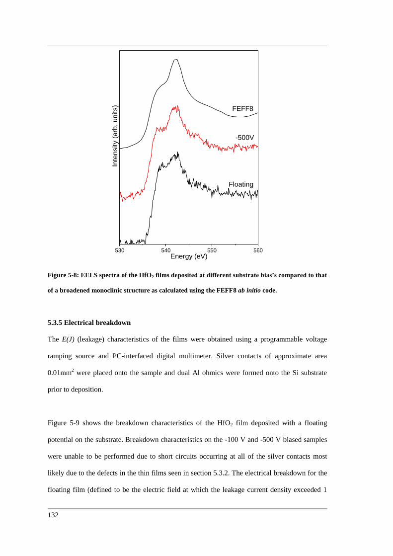
132
530 540 550 560
Floating
-500V
FEFF8
Inte
nsity (
arb
. u
nits)
Energy (eV)
Figure 5-8: EELS spectra of the HfO2 films deposited at different substrate bias’s compared to that
of a broadened monoclinic structure as calculated using the FEFF8 ab initio code.
5.3.5 Electrical breakdown
The E(J) (leakage) characteristics of the films were obtained using a programmable voltage
ramping source and PC-interfaced digital multimeter. Silver contacts of approximate area
0.01mm2 were placed onto the sample and dual Al ohmics were formed onto the Si substrate
prior to deposition.
Figure 5-9 shows the breakdown characteristics of the HfO2 film deposited with a floating
potential on the substrate. Breakdown characteristics on the -100 V and -500 V biased samples
were unable to be performed due to short circuits occurring at all of the silver contacts most
likely due to the defects in the thin films seen in section 5.3.2. The electrical breakdown for the
floating film (defined to be the electric field at which the leakage current density exceeded 1
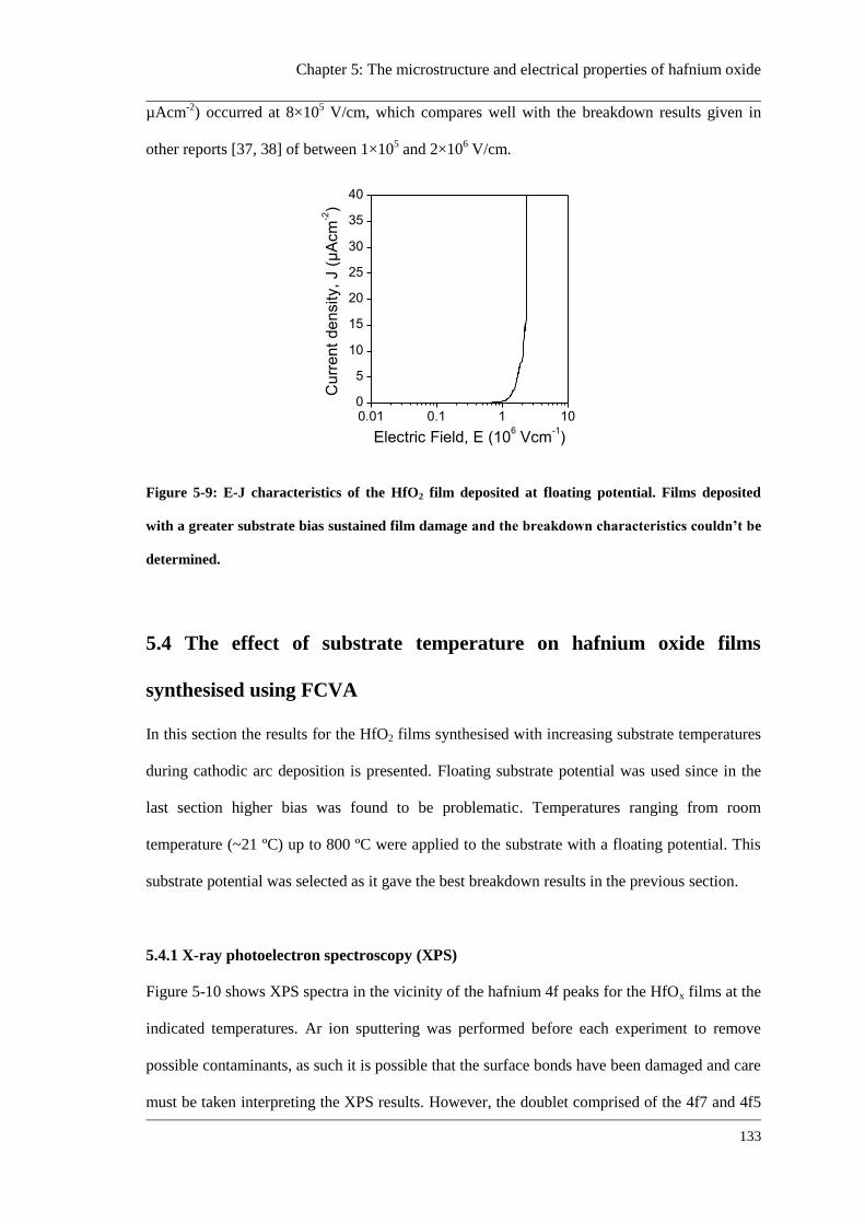
Chapter 5: The microstructure and electrical properties of hafnium oxide
133
µAcm-2
) occurred at 8×10⁵ V/cm, which compares well with the breakdown results given in
other reports [37, 38] of between 1×10⁵ and 2×10
6 V/cm.
0.01 0.1 1 100
5
10
15
20
25
30
35
40
Curr
ent
density,
J (
µA
cm
-2)
Electric Field, E (106 Vcm
-1)
Figure 5-9: E-J characteristics of the HfO2 film deposited at floating potential. Films deposited
with a greater substrate bias sustained film damage and the breakdown characteristics couldn’t be
determined.
5.4 The effect of substrate temperature on hafnium oxide films
synthesised using FCVA
In this section the results for the HfO2 films synthesised with increasing substrate temperatures
during cathodic arc deposition is presented. Floating substrate potential was used since in the
last section higher bias was found to be problematic. Temperatures ranging from room
temperature (~21 ºC) up to 800 ºC were applied to the substrate with a floating potential. This
substrate potential was selected as it gave the best breakdown results in the previous section.
5.4.1 X-ray photoelectron spectroscopy (XPS)
Figure 5-10 shows XPS spectra in the vicinity of the hafnium 4f peaks for the HfOx films at the
indicated temperatures. Ar ion sputtering was performed before each experiment to remove
possible contaminants, as such it is possible that the surface bonds have been damaged and care
must be taken interpreting the XPS results. However, the doublet comprised of the 4f7 and 4f5
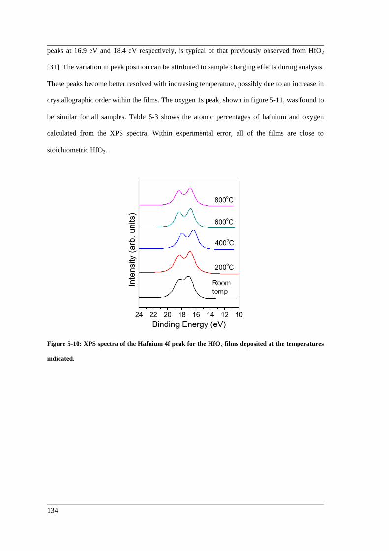
134
peaks at 16.9 eV and 18.4 eV respectively, is typical of that previously observed from HfO2
[31]. The variation in peak position can be attributed to sample charging effects during analysis.
These peaks become better resolved with increasing temperature, possibly due to an increase in
crystallographic order within the films. The oxygen 1s peak, shown in figure 5-11, was found to
be similar for all samples. Table 5-3 shows the atomic percentages of hafnium and oxygen
calculated from the XPS spectra. Within experimental error, all of the films are close to
stoichiometric HfO2.
24 22 20 18 16 14 12 10
Inte
nsity (
arb
. units)
Binding Energy (eV)
Room
temp
200oC
400oC
600oC
800oC
Figure 5-10: XPS spectra of the Hafnium 4f peak for the HfOx films deposited at the temperatures
indicated.
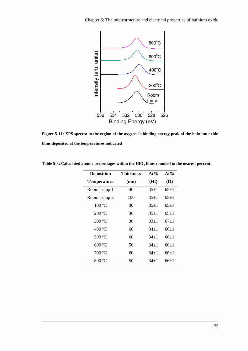
Chapter 5: The microstructure and electrical properties of hafnium oxide
135
536 534 532 530 528 526
Inte
nsity (
arb
. u
nits)
Binding Energy (eV)
Room
temp
200oC
400oC
600oC
800oC
Figure 5-11: XPS spectra in the region of the oxygen 1s binding energy peak of the hafnium oxide
films deposited at the temperatures indicated
Table 5-3: Calculated atomic percentages within the HfO2 films rounded to the nearest percent.
Deposition
Temperature
Thickness
(nm)
At%
(Hf)
At%
(O)
Room Temp 1 40 35±1 65±1
Room Temp 2 100 35±1 65±1
100 ºC 30 35±1 65±1
200 ºC 30 35±1 65±1
300 ºC 30 33±1 67±1
400 ºC 60 34±1 66±1
500 ºC 60 34±1 66±1
600 ºC 50 34±1 66±1
700 ºC 60 34±1 66±1
800 ºC 50 34±1 66±1
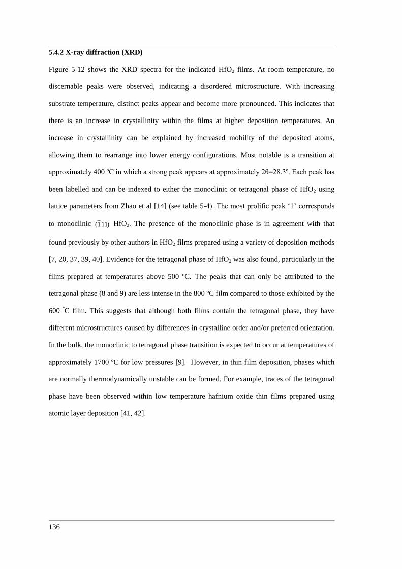
136
5.4.2 X-ray diffraction (XRD)
Figure 5-12 shows the XRD spectra for the indicated HfO2 films. At room temperature, no
discernable peaks were observed, indicating a disordered microstructure. With increasing
substrate temperature, distinct peaks appear and become more pronounced. This indicates that
there is an increase in crystallinity within the films at higher deposition temperatures. An
increase in crystallinity can be explained by increased mobility of the deposited atoms,
allowing them to rearrange into lower energy configurations. Most notable is a transition at
approximately 400 ºC in which a strong peak appears at approximately 2θ=28.3º. Each peak has
been labelled and can be indexed to either the monoclinic or tetragonal phase of HfO2 using
lattice parameters from Zhao et al [14] (see table 5-4). The most prolific peak ‘1’ corresponds
to monoclinic )111( HfO2. The presence of the monoclinic phase is in agreement with that
found previously by other authors in HfO2 films prepared using a variety of deposition methods
[7, 20, 37, 39, 40]. Evidence for the tetragonal phase of HfO2 was also found, particularly in the
films prepared at temperatures above 500 ºC. The peaks that can only be attributed to the
tetragonal phase (8 and 9) are less intense in the 800 ºC film compared to those exhibited by the
600 ºC film. This suggests that although both films contain the tetragonal phase, they have
different microstructures caused by differences in crystalline order and/or preferred orientation.
In the bulk, the monoclinic to tetragonal phase transition is expected to occur at temperatures of
approximately 1700 ºC for low pressures [9]. However, in thin film deposition, phases which
are normally thermodynamically unstable can be formed. For example, traces of the tetragonal
phase have been observed within low temperature hafnium oxide thin films prepared using
atomic layer deposition [41, 42].
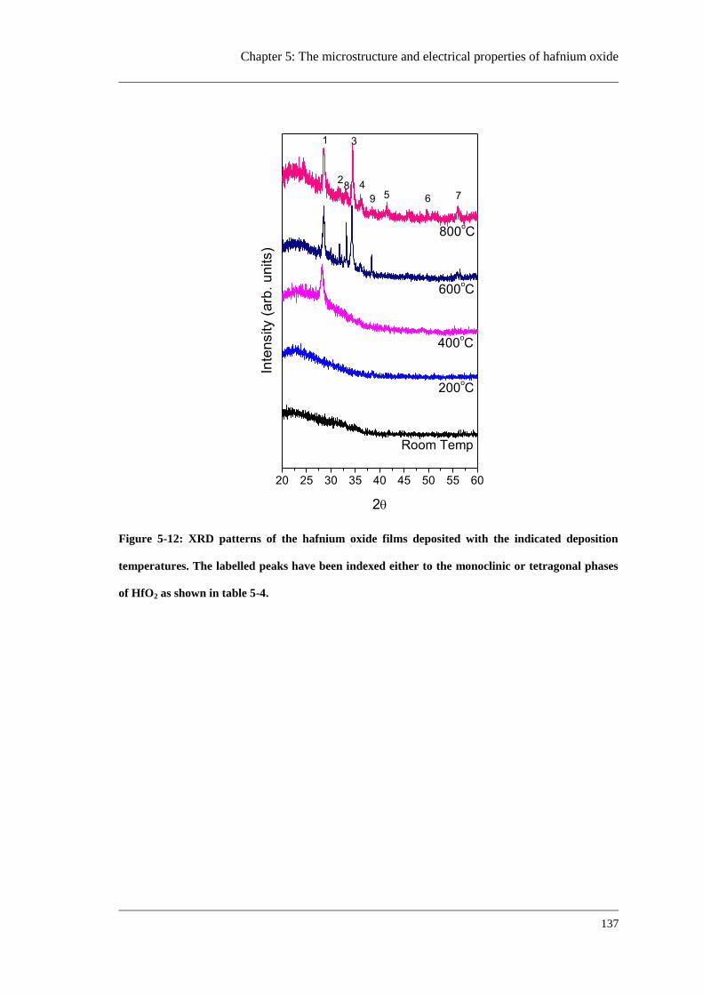
Chapter 5: The microstructure and electrical properties of hafnium oxide
137
20 25 30 35 40 45 50 55 60
8
9
20 25 30 35 40 45 50 55 60
10
9
8765
4
32
Inte
nsity (
arb
. u
nits)
2
800oC
600oC
400oC
200oC
Room Temp
1
7654
3
2
Inte
nsity (
arb
. u
nits)
2
800oC
600oC
400oC
200oC
Room Temp
1
Figure 5-12: XRD patterns of the hafnium oxide films deposited with the indicated deposition
temperatures. The labelled peaks have been indexed either to the monoclinic or tetragonal phases
of HfO2 as shown in table 5-4.
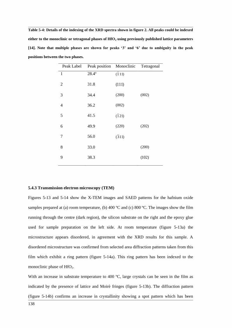
138
Table 5-4: Details of the indexing of the XRD spectra shown in figure 2. All peaks could be indexed
either to the monoclinic or tetragonal phases of HfO2 using previously published lattice parameters
[14]. Note that multiple phases are shown for peaks ‘3’ and ‘6’ due to ambiguity in the peak
positions between the two phases.
Peak Label Peak position Monoclinic Tetragonal
1 28.4º )111(
2 31.8 )111(
3 34.4 )200( )002(
4 36.2 )002(
5 41.5 )211(
6 49.9 )220( )202(
7 56.0 )113(
8 33.0 )200(
9 38.3 )102(
5.4.3 Transmission electron microscopy (TEM)
Figures 5-13 and 5-14 show the X-TEM images and SAED patterns for the hafnium oxide
samples prepared at (a) room temperature, (b) 400 ºC and (c) 800 ºC. The images show the film
running through the centre (dark region), the silicon substrate on the right and the epoxy glue
used for sample preparation on the left side. At room temperature (figure 5-13a) the
microstructure appears disordered, in agreement with the XRD results for this sample. A
disordered microstructure was confirmed from selected area diffraction patterns taken from this
film which exhibit a ring pattern (figure 5-14a). This ring pattern has been indexed to the
monoclinic phase of HfO2.
With an increase in substrate temperature to 400 ºC, large crystals can be seen in the film as
indicated by the presence of lattice and Moirè fringes (figure 5-13b). The diffraction pattern
(figure 5-14b) confirms an increase in crystallinity showing a spot pattern which has been
Chapter 5: The microstructure and electrical properties of hafnium oxide
139
indexed to the monoclinic phase. The image and diffraction pattern (figures 5-13c and 5-14c)
shows that the film deposited at 800 ºC also contains a high degree of crystal order. The
diffraction pattern has been indexed to the monoclinic phase, however many of the spots could
not be unambiguously indexed, suggesting the presence of multiple phases present within the
film.
Figure 5-13: X-TEM images of the HfO2 films prepared with substrate temperatures of (a) room
temperature, (b) 400 ºC and (c) 800 ºC. The HfO2 film is the dark region running down the centre
of each image, the silicon substrate is on the right hand side and the epoxy bonding agent is on the
left hand side.
(a) RT
(b) 400ºC
(c) 800ºC
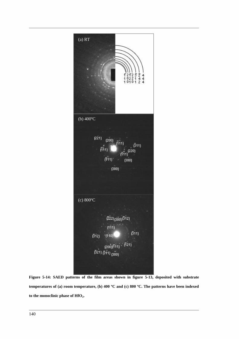
140
Figure 5-14: SAED patterns of the film areas shown in figure 5-13, deposited with substrate
temperatures of (a) room temperature, (b) 400 ºC and (c) 800 ºC. The patterns have been indexed
to the monoclinic phase of HfO2.
(a) RT
(b) 400ºC
(c) 800ºC
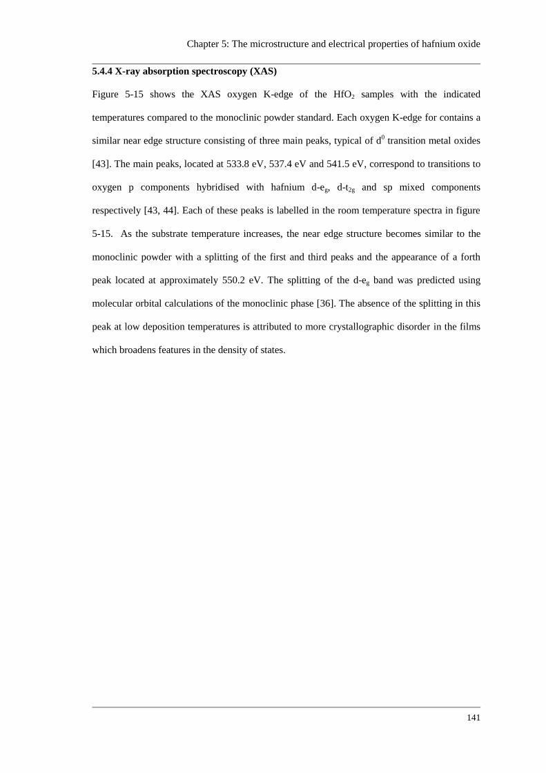
Chapter 5: The microstructure and electrical properties of hafnium oxide
141
5.4.4 X-ray absorption spectroscopy (XAS)
Figure 5-15 shows the XAS oxygen K-edge of the HfO2 samples with the indicated
temperatures compared to the monoclinic powder standard. Each oxygen K-edge for contains a
similar near edge structure consisting of three main peaks, typical of d0 transition metal oxides
[43]. The main peaks, located at 533.8 eV, 537.4 eV and 541.5 eV, correspond to transitions to
oxygen p components hybridised with hafnium d-eg, d-t2g and sp mixed components
respectively [43, 44]. Each of these peaks is labelled in the room temperature spectra in figure
5-15. As the substrate temperature increases, the near edge structure becomes similar to the
monoclinic powder with a splitting of the first and third peaks and the appearance of a forth
peak located at approximately 550.2 eV. The splitting of the d-eg band was predicted using
molecular orbital calculations of the monoclinic phase [36]. The absence of the splitting in this
peak at low deposition temperatures is attributed to more crystallographic disorder in the films
which broadens features in the density of states.
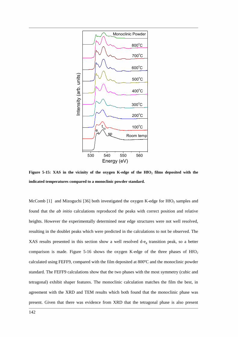
142
530 540 550 560
spe
g
Room temp
Monoclinic Powder
800oC
700oC
600oC
500oC
400oC
300oC
200oCIn
ten
sity (
arb
. u
nits)
Energy (eV)
100oCt
2g
Figure 5-15: XAS in the vicinity of the oxygen K-edge of the HfO2 films deposited with the
indicated temperatures compared to a monoclinic powder standard.
McComb [1] and Mizoguchi [36] both investigated the oxygen K-edge for HfO2 samples and
found that the ab initio calculations reproduced the peaks with correct position and relative
heights. However the experimentally determined near edge structures were not well resolved,
resulting in the doublet peaks which were predicted in the calculations to not be observed. The
XAS results presented in this section show a well resolved d-eg transition peak, so a better
comparison is made. Figure 5-16 shows the oxygen K-edge of the three phases of HfO2
calculated using FEFF9, compared with the film deposited at 800ºC and the monoclinic powder
standard. The FEFF9 calculations show that the two phases with the most symmetry (cubic and
tetragonal) exhibit shaper features. The monoclinic calculation matches the film the best, in
agreement with the XRD and TEM results which both found that the monoclinic phase was
present. Given that there was evidence from XRD that the tetragonal phase is also present
Chapter 5: The microstructure and electrical properties of hafnium oxide
143
within the films deposited at higher temperatures, a linear combination of phases (60%
monoclinic, 40% tetragonal) is also plotted in figure 5-16. It can be seen that this combined
spectra is a better fit, particularly the d-t2g peak.
530 540 550 560
FEFF9 - Mix
Monoclinic Powder
FEFF9 - Cubic
FEFF9 - Tetragonal
Inte
nsity (
arb
. units)
Energy (eV)
FEFF9 - Monoclinic
XAS - 800oC
Figure 5-16: Comparison of the oxygen K-edge for the FEFF9 calculations of 3 phases of HfO2
compared to the 800ºC HfO2 sample and monoclinic powder standard. The spectra ‘FEFF9 – Mix’
refers to a 3:2 linear combination of the monoclinic phase and the tetragonal phase.
5.4.5 Electrical breakdown
Figure 5-17 shows the electrical breakdown characteristics, E(J) for selected HfO2 films. Table
5-5 lists the breakdown field for each of the samples. With the notable exception of the film
deposited at 800 °C, there is a correlation between growth temperature and the breakdown
characteristics of the films. As the substrate temperature increases and the crystallinity
improves, the breakdown characteristics tend to degrade. These results support the proposition
that disordered films provide the best breakdown characteristics in HfO2 films [15-18]. The
weaker breakdown characteristic exhibited by the film deposited at 600 °C compared to that
exhibited by the film deposited at 800 °C can be attributed to the differences in microstructure
apparent in the XRD results. The electrical breakdown for the film deposited at room
temperature (defined to be the electric field at which the leakage current density exceeded 1
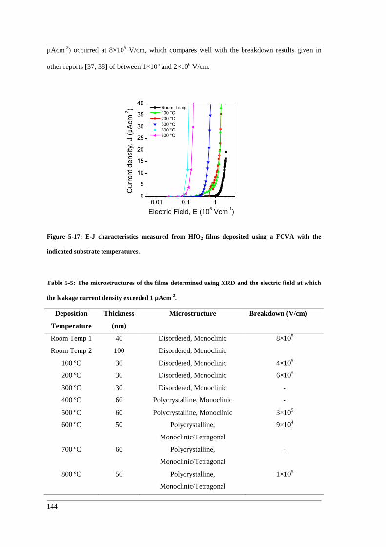
144
µAcm-2
) occurred at 8×10⁵ V/cm, which compares well with the breakdown results given in
other reports [37, 38] of between 1×10⁵ and 2×10
6 V/cm.
0.01 0.1 10
5
10
15
20
25
30
35
40
Cu
rre
nt
de
nsity,
J (
µA
cm
-2)
Electric Field, E (106 Vcm
-1)
Room Temp
100 °C
200 °C
500 °C
600 °C
800 °C
Figure 5-17: E-J characteristics measured from HfO2 films deposited using a FCVA with the
indicated substrate temperatures.
Table 5-5: The microstructures of the films determined using XRD and the electric field at which
the leakage current density exceeded 1 µAcm-2
.
Deposition
Temperature
Thickness
(nm)
Microstructure Breakdown (V/cm)
Room Temp 1 40 Disordered, Monoclinic 8×10⁵
Room Temp 2 100 Disordered, Monoclinic
100 ºC 30 Disordered, Monoclinic 4×10⁵
200 ºC 30 Disordered, Monoclinic 6×10⁵
300 ºC 30 Disordered, Monoclinic -
400 ºC 60 Polycrystalline, Monoclinic -
500 ºC 60 Polycrystalline, Monoclinic 3×10⁵
600 ºC 50 Polycrystalline,
Monoclinic/Tetragonal
9×10⁴
700 ºC 60 Polycrystalline,
Monoclinic/Tetragonal
-
800 ºC 50 Polycrystalline,
Monoclinic/Tetragonal
1×10⁵
Chapter 5: The microstructure and electrical properties of hafnium oxide
145
5.6 Conclusions
In this chapter, the microstructure and breakdown characteristic of hafnium oxide films
prepared using FCVA were investigated as a function of (1) substrate bias and (2) substrate
temperature. It was found that with increasing bias on the substrate during deposition that the
coatings electrically discharged, causing significant damage to the structure of the films leaving
pin holes and large defects. Films deposited at floating potential were found to exhibit good
breakdown performance comparable to other work, showing that the FCVA method is capable
of producing high quality hafnium oxide films.
With increasing substrate temperature, there is an increase in mobility of the deposited atoms
which promotes crystallisation. Diffraction analysis of the films showed that the dominant
phase present was monoclinic HfO2, although there was evidence for the presence of the high
temperature tetragonal phase at higher substrate temperatures. It was found that the electrical
breakdown of the films was dependent on the substrate temperature and hence crystallinity in
the films. Increased crystallinity resulted in a lowering of the electrical breakdown, supporting
the proposition that disordered films are preferable for gate dielectric applications.
5.7 Bibliography
1. McComb, D.W., A.J. Craven, D.A. Hamilton, and M. MacKenzie, Probing local
coordination environments in high-k materials for gate stack applications. Applied
Physics Letters, 2004. 84(22): p. 4523-4525.
2. Wilk, G.D., R.M. Wallace, and J.M. Anthony, High- gate dielectrics: Current status
and materials properties considerations. Journal of Applied Physics, 2001. 89(10): p.
5243-5275.
3. Chau, R., J. Brask, S. Datta, G. Dewey, M. Doczy, B. Doyle, J. Kavalieros, B. Jin, M.
Metz, A. Majumdar, and M. Radosavljevic, Application of high- gate dielectrics and
metal gate electrodes to enable silicon and non-silicon logic nanotechnology.
Microelectronic Engineering, 2005. 80: p. 1-6.
4. Chau, R., S. Datta, M. Doczy, J. Kavalieros, and M. Metz, Gate Dielectric Scaling for
High-Performance CMOS: from SiO2 to High-, in Extended Abstracts of International
Workshop on Gate Insulator (IWGI). November 2003, pp. 124-126: Tokyo, Japan.
5. Foran, B., J. Barnett, P.S. Lysaght, M.P. Agustin, and S. Stemmer, Characterization of
advanced gate stacks for Si CMOS by electron energy-loss spectroscopy in scanning
146
transmission electron microscopy. Journal of Electron Spectroscopy and Related
Phenomena, 2005. 143(2-3): p. 149-158.
6. Ohta, H. and H. Hosono, Transparent oxide optoelectronics. Materials Today, 2004.
7(6): p. 42-51.
7. Haines, J., J.M. Leger, S. Hull, J.P. Petitet, A.S. Pereira, C.A. Perottoni, and J.A.H. Da
Jornada, ChemInform Abstract: Characterization of the Cotunnite-Type Phases of
Zirconia and Hafnia by Neutron Diffraction and Raman Spectroscopy. ChemInform,
1997. 28(42): p. no-no.
8. Cheynet, M.C., S. Pokrant, F.D. Tichelaar, and J.-L. Rouviere, Crystal structure and
band gap determination of HfO[sub 2] thin films. Journal of Applied Physics, 2007.
101(5): p. 054101-8.
9. Wang, J., H.P. Li, and R. Stevens, Hafnia and hafnia-toughened ceramics. Journal of
Materials Science, 1992. 27(20): p. 5397-5430.
10. He, J.Q., A. Teren, C.L. Jia, P. Ehrhart, K. Urban, R. Waser, and R.H. Wang,
Microstructure and interfaces of HfO2 thin films grown on silicon substrates. Journal
of Crystal Growth, 2004. 262(1-4): p. 295-303.
11. Niinistö, J., M. Mäntymäki, K. Kukli, L. Costelle, E. Puukilainen, M. Ritala, and M.
Leskelä, Growth and phase stabilization of HfO2 thin films by ALD using novel
precursors. Journal of Crystal Growth, 2010. 312(2): p. 245-249.
12. Ushakov, S.V., A. Navrotsky, Y. Yang, S. Stemmer, K. Kukli, M. Ritala, M.A.
Leskelä, P. Fejes, A. Demkov, C. Wang, B.Y. Nguyen, D. Triyoso, and P. Tobin,
Crystallization in hafnia- and zirconia-based systems. physica status solidi (b), 2004.
241(10): p. 2268-2278.
13. Lowther, J.E., J.K. Dewhurst, J.M. Leger, and J. Haines, Relative stability of ZrO2 and
HfO2 structural phases. Physical Review B, 1999. 60(21): p. 14485.
14. Zhao, X. and D. Vanderbilt, First-principles study of structural, vibrational, and lattice
dielectric properties of hafnium oxide. Physical Review B, 2002. 65(23): p. 233106.
15. Forsgren, K., A. Harsta, J. Aarik, A. Aidla, J. Westlinder, and J. Olsson, Deposition of
HfO2 Thin Films in HfI4-Based Processes. Journal of The Electrochemical Society,
2002. 149(10): p. F139-F144.
16. Rangarajan, V., H. Bhandari, and T.M. Klein, Comparison of hafnium silicate thin
films on silicon (1 0 0) deposited using thermal and plasma enhanced metal organic
chemical vapor deposition. Thin Solid Films, 2002. 419(1-2): p. 1-4.
17. Moon Sig, J., C. Byung Jin, Y. Chia Ching, D. Siu Hung Chan, W. Sung Jin, S.
Mathew, L. Kanta Bera, N. Balasubramanian, and K. Dim-Lee, Formation of hafnium-
aluminum-oxide gate dielectric using single cocktail liquid source in MOCVD process.
Electron Devices, IEEE Transactions on, 2003. 50(10): p. 2088-2094.
18. Choi, C.H., S.J. Rhee, T.S. Jeon, N. Lu, J.H. Sim, R. Clark, M. Niwa, and D.L. Kwong.
Thermally stable CVD HfOxNy advanced gate dielectrics with poly-Si gate electrode. in
Electron Devices Meeting, 2002. IEDM '02. Digest. International. 2002.
19. Hergenrother, J.M., G.D. Wilk, T. Nigam, F.P. Klemens, D. Monroe, P.J. Silverman,
T.W. Sorsch, B. Busch, M.L. Green, M.R. Baker, T. Boone, M.K. Bude, N.A. Ciampa,
E.J. Ferry, A.T. Fiory, S.J. Hillenius, D.C. Jacobson, R.W. Johnson, P. Kalavade, R.
Keller, C.A. King, A. Kornblit, H.W. Krautter, J.T.C. Lee, W.M. Mansfield, J.F.
Miner, M.D. Morris, S.H. Oh, J.M. Rosamilia, B.J. Sapjeta, K. Short, K. Steiner, D.A.
Muller, P.M. Voyles, J.L. Grazul, E. Shero, M.E. Givens, C. Pomarede, M. Mazanec,
and C. Werkhoven. 50 nm vertical replacement-gate (VRG) nMOSFETs with ALD
HfO2 and Al2O3 gate dielectrics. in Electron Devices Meeting, 2001. IEDM Technical
Digest. International. 2001.
20. Ho, M.Y., H. Gong, G.D. Wilk, B.W. Busch, M.L. Green, P.M. Voyles, D.A. Muller,
M. Bude, W.H. Lin, A. See, M.E. Loomans, S.K. Lahiri, and P.I. Raisanen,
Morphology and crystallization kinetics in HfO2 thin films grown by atomic layer
deposition. Journal of Applied Physics, 2003. 93(3): p. 1477-1481.
Chapter 5: The microstructure and electrical properties of hafnium oxide
147
21. Nguyen, N.V., V.D. Albert, C.-H. Deane, and M.F. Martin, Sub-bandgap defect states
in polycrystalline hafnium oxide and their suppression by admixture of silicon. Applied
Physics Letters, 2005. 87(19): p. 192903.
22. Ratzke, M., D. Wolfframm, M. Kappa, S. Kouteva-Arguirova, and J. Reif, Pulsed laser
deposition of HfO2 and PrxOy high-k films on Si(100). Applied Surface Science, 2005.
247(1-4): p. 128-133.
23. Yu. Yu, L., A. Zenkevich, E.P. Gusev, and M. Gribelyuk, In situ investigation of
growth and thermal stability of ultrathin Si layers on the HfO[sub 2]/Si (100) high-
kappa dielectric system. Applied Physics Letters, 2005. 86(19): p. 191904.
24. Balog, M., Chemical vapor deposition and characterization of HfO2 films from
organo-hafnium compounds. Thin Solid Films, 1977. 41(3): p. 247-259.
25. Al-Kuhaili, M.F., Optical properties of hafnium oxide thin films and their application
in energy-efficient windows. Optical Materials, 2004. 27(3): p. 383-387.
26. Filipescu, M., N. Scarisoreanu, V. Craciun, B. Mitu, A. Purice, A. Moldovan, V. Ion,
O. Toma, and M. Dinescu, High-k dielectric oxides obtained by PLD as solution for
gates dielectric in MOS devices. Applied Surface Science, 2007. 253(19): p. 8184-
8191.
27. Grüger, H., C. Kunath, E. Kurth, S. Sorge, W. Pufe, and T. Pechstein, High quality r.f.
sputtered metal oxides (Ta2O5, HfO2) and their properties after annealing. Thin Solid
Films, 2004. 447-448: p. 509-515.
28. Tay, B.K., Z.W. Zhao, and D.H.C. Chua, Review of metal oxide films deposited by
filtered cathodic vacuum arc technique. Materials Science and Engineering: R:
Reports, 2006. 52(1-3): p. 1-48.
29. Lau, D.W.M., D.G. McCulloch, M.B. Taylor, J.G. Partridge, D.R. McKenzie, N.A.
Marks, E.H.T. Teo, and B.K. Tay, Abrupt Stress Induced Transformation in
Amorphous Carbon Films with a Highly Conductive Transition Phase. Physical
Review Letters, 2008. 100(17): p. 176101.
30. Biluš Abaffy, N., J.G. Partridge, J. du Plessis, and D.G. McCulloch, Optically
absorbing trilayer films fabricated using a Filtered Cathodic Vacuum Arc. Physica
Status Solidi (a), 2008. 205(6): p. 1439-1442.
31. Smirnova, T., V. Kaichev, L. Yakovkina, V. Kosyakov, S. Beloshapkin, F. Kuznetsov,
M. Lebedev, and V. Gritsenko, Composition and structure of hafnia films on silicon.
Inorganic Materials, 2008. 44(9): p. 965-970.
32. Tan, S., Control of Interface Traps in HfO<sub>2</sub> Gate Dielectric
on Silicon. Journal of Electronic Materials, 2010. 39(11): p. 2435-2440.
33. Hullavarad, S., D. Pugel, E. Jones, R. Vispute, and T. Venkatesan, Low Leakage
Current Transport and High Breakdown Strength of Pulsed Laser Deposited
HfO<sub>2</sub>/SiC Metal-Insulator-Semiconductor Device Structures.
Journal of Electronic Materials, 2007. 36(6): p. 648-653.
34. Watts, J.F. and J. Wolstenholme, An Introduction to Surface Analysis by XPS and AES.
2003: Wiley.
35. Gan, B.K., M.M.M. Bilek, D.R. McKenzie, Y. Shi, D.A. Tompsett, M.B. Taylor, and
D.G. McCulloch, Stress relief and texture formation in aluminium nitride by plasma
immersion ion implantation. Journal of Physics: Condensed Matter, 2004. 10: p. 1751.
36. Mizoguchi, T. and et al., First-principles calculation of oxygen K-electron energy loss
near edge structure of HfO2. Journal of Physics: Condensed Matter, 2009. 21(10): p.
104212.
37. Dueñas, S., H. Castán, H. García, A. Gómez, L. Bailón, M. Toledano-Luque, I. Mártil,
and G. González-Díaz, Electrical properties of high-pressure reactive sputtered thin
hafnium oxide high-k gate dielectrics. Semiconductor Science and Technology,
2007(12): p. 1344.
38. Yang, T.S., K.-S. An, E.-J. Lee, W. Cho, H.S. Jang, S.K. Park, Y.K. Lee, T.-M. Chung,
C.G. Kim, S. Kim, J.-H. Hwang, C. Lee, N.-S. Lee, and Y. Kim, Chemical Vapor
Deposition of HfO2 Thin Films Using the Novel Single Precursor Hafnium 3-Methyl-3-
pentoxide, Hf(mp)4. Chemistry of Materials, 2005. 17(26): p. 6713-6718.
148
39. Scarel, G., S. Spiga, C. Wiemer, G. Tallarida, S. Ferrari, and M. Fanciulli, Trends of
structural and electrical properties in atomic layer deposited HfO2 films. Materials
Science and Engineering B, 2004. 109(1-3): p. 11-16.
40. Ni, J., Z.-c. Li, and Z.-j. Zhang, Influence of deposition temperature on the structure
and optical properties of HfO2 thin films. Frontiers of Materials Science in China,
2008. 2(4): p. 381-385.
41. Aarik, J., A. Aidla, A.A. Kiisler, T. Uustare, and V. Sammelselg, Influence of substrate
temperature on atomic layer growth and properties of HfO2 thin films. Thin Solid
Films, 1999. 340(1-2): p. 110-116.
42. Nguyen, N.V., A.V. Davydov, D. Chandler-Horowitz, and M.M. Frank, Sub-bandgap
defect states in polycrystalline hafnium oxide and their suppression by admixture of
silicon. Applied Physics Letters, 2005. 87(19): p. 192903-3.
43. Chen, J.G., NEXAFS investigations of transition metal oxides, nitrides, carbides,
sulfides and other interstitial compounds. Surface Science Reports, 1997. 30(1-3): p. 1-
152.
44. Soriano, L., M. Abbate, J.C. Fuggle, M.A. Jiménez, J.M. Sanz, C. Mythen, and H.A.
Padmore, The O 1s x-ray absorption spectra of transition-metal oxides: The TiO2-
ZrO2-HfO2 and V2O5-Nb2O5-Ta2O5 series. Solid State Communications, 1993. 87(8): p.
699-703.
Conclusions and future work
149
Chapter 6
Conclusions and future work
Metal oxide thin films play an important role in many industries and have been extensively
studied for decades. From the discovery of tungsten bronzes to the use of hafnium silicates in
microprocessors in modern computing, these materials are not only of major interest to the
scientific community but also in industry for the betterment of modern living. However, with a
vast array of materials and means of thin film coating deposition available, the growth
mechanics of a particular deposition method and the effect on the properties of the films is not
well understood. It may be expected that thin film coatings with similar properties will be
attained independent of deposition method. However, seemingly small differences often play a
role in changing the microstructure which result in surprisingly large variations in the physical
properties of the films.
This thesis investigates the microstructure and physical properties of several important metal
oxide coatings. Several deposition techniques were employed and the effect of changing the
deposition conditions investigated.
In chapter 3, tungsten oxide (WO3) films were synthesised using both pulsed cathodic arc and
pulsed magnetron sputtering deposition techniques. The effect of deposition method on the
microstructure of the films was investigated using electron microscopy and spectroscopic
techniques. Ab initio calculations were performed to study the change in the near edge structure
150
for different microstructures and this was used to fingerprint the phases of the deposited films.
From these results, the major findings were:
1. Dependence on deposition method of the microstructure of WO3 films.
It was found that the energetic deposition from the pulsed arc resulted in a highly
ordered tetragonal microstructure. In contrast to this with magnetron sputtering,
deposition by low energy neutrals, a highly disordered film was deposited. These
results demonstrate how different deposition techniques can lead to films with
completely different microstructures.
2. Using ab initio calculations to fingerprint the microstructure of WO3 films.
It was shown using the ab initio codes that the near edge structure of known phases of
WO3 could be calculated. This calculated near edge structure can be used as a
fingerprint to match with experimental results to help identify the phase present.
In chapter 4 the physical properties and microstructure of aluminium zinc oxide films (AZO)
films were investigated. AZO films were deposited using pulsed cathodic arc, pulsed
magnetron sputtering, high power impulse magnetron sputtering (HIPIMS) and a novel variant
of HIPIMS which incorporated a straight magnetic filter. The major findings for this chapter
are presented below:
1. Relationship between microstructure and the physical properties of AZO films.
It was found that depending on microstructure of the deposited AZO films, different
optical and electrical properties could be observed. Each of the coatings appeared as
wurtite ZnO with different amounts of crystallographic order depending on the
deposition method. It was found that much of the aluminium appeared within the AZO
films not as substitutional Al in Zn sites, but instead in the form of octahedrally
arranged -Al2O3. Coatings with a disordered microstructure exhibited inferior
electrical properties as opposed to those which contained wurtzite ZnO grains oriented
with their c-axis perpendicular to the substrate which performed best.

Conclusions and future work
151
2. Negative ion damage and its effect on the structure and properties of AZO films.
It was shown that the presence of O- ions during reactive deposition of AZO coatings
in magnetron sputtering related techniques had a negative influence on film properties.
Depending on the position on the substrate in relation to the magnetron field lines,
different amounts of ion damage was observed. This ion damage effect was
exacerbated in the HIPIMS technique which uses much higher power, thus accelerating
the damaging ions with a greater energy. As a result of this ion damage, the electrical
and optical properties of the films were compromised. It was shown that using a
magnetic filter during deposition acts to protect the AZO films from the negative ion
impacts and also enhances deposition rates.
Filtered cathodic vacuum arc (FCVA) was shown to be a good method for depositing dense,
flat hafnium oxide (HfO2) films. In chapter 5 the effect of increased deposition temperature and
substrate bias on the microstructure and electrical breakdown of FCVA deposited HfO2 films
was investigated. The major findings for this chapter are presented below:
1. The relationship between crystallinity and electrical breakdown of HfO2 films. The
temperature dependence on the crystallinity was explored and it was found that phases
which are usually thermodynamically unstable can be achieved with thin film coatings.
It was shown that the amount of crystallinity of the HfO2 films has a direct effect on the
electrical breakdown, whereby disordered films deposited at room temperature were
found to have the best breakdown characteristics compared to the crystallised films
deposited at higher temperatures.
152
From the work completed and the findings in this thesis, there is still much in this field to be
explored. Some suggestions for future research include:
1. Perform transmission electron microscopy on the AZO films prepared by magnetron
sputtering, HIPIMS and filtered HIPIMS.
2. Further work on the effect of negative ion damage on the structure of the films. It will
be possible to apply this knowledge to other materials which will be useful to other
research groups and industry to make thin film coatings with superior performance.
3. Perform C(V) measurements on HfO2 films deposited by cathodic arc to analyse how
the differences in crystallinity affect the dielectric constant for this films.
4. Deposit HfO2 films of thickness in the order of 10-20 nm using a filtered cathodic arc
to determine the effect on crystallinity and electrical properties of miniaturisation of the
films. The work in the AZO chapter revealed that it is possible to grow films where the
crystal grains take up the entirety of the thickness of the films. If this were applied to
HfO2 films, it might be possible to grow films where the relative size of the crystals to
the film thickness is large, thereby reducing the grain boundaries and possible leakage
paths.


![[TA1-D] Hybrid Oxide Thin Films](https://static.fdocuments.in/doc/165x107/615ab33bad71057f9352b7b6/ta1-d-hybrid-oxide-thin-films.jpg)