The evolution of electronic structure in few-layer graphene
6
The evolution of electronic structure in few-layer graphene revealed by optical spectroscopy Kin Fai Mak a , Matthew Y. Sfeir b , James A. Misewich b , and Tony F. Heinz a,1 a Departments of Physics and Electrical Engineering, Columbia University, New York, NY 10027; and b Brookhaven National Laboratory, Upton, NY 11973 Edited by Mildred Dresselhaus, Massachusetts Institute of Technology, Cambridge, MA, and approved July 8, 2010 (received for review April 5, 2010) The massless Dirac spectrum of electrons in single-layer graphene has been thoroughly studied both theoretically and experimen- tally. Although a subject of considerable theoretical interest, experimental investigations of the richer electronic structure of few-layer graphene (FLG) have been limited. Here we examine FLG graphene crystals with Bernal stacking of layer thicknesses N ¼ 1,2,3,…8 prepared using the mechanical exfoliation technique. For each layer thickness N, infrared conductivity measurements over the spectral range of 0.2–1.0 eV have been performed and reveal a distinctive band structure, with different conductivity peaks present below 0.5 eV and a relatively flat spectrum at higher photon energies. The principal transitions exhibit a systematic energy-scaling behavior with N. These observations are explained within a unified zone-folding scheme that generates the electronic states for all FLG materials from that of the bulk 3D graphite crystal through imposition of appropriate boundary conditions. Using the Kubo formula, we find that the complete infrared conductivity spectra for the different FLG crystals can be reproduced reasonably well within the framework a tight-binding model. electronic structures ∣ infrared spectroscopy ∣ zone-folding method T he unique electronic properties of graphene, a single-mono- layer of sp 2 -hybridized carbon, have attracted much attention (1). Graphene’s few-layer counterparts have also recently been the subject of much interest, since this broader class of materials offers the potential for further control of electronic states by in- terlayer interactions (2–6). Indeed, theoretical investigations have predicted dramatic changes in the electronic properties in few-layer graphene (FLG) compared with single-layer gra- phene (SLG) (7–17): When two or more layers of graphene are present in ordered FLG, the characteristic linearly dispersing bands of the single layer are either replaced or augmented by pairs of split hyperbolic bands. These new bands correspond to fermions of finite mass, unlike the electrons present in SLG that behave as massless fermions. Further, the characteristics of the electrons in FLG are expected to change sensitively with in- creasing layer number N, before ultimately approaching the bulk limit of graphite. Despite these fascinating predictions, experi- mental investigations have been limited to SLG and a few studies of the electronic properties of bilayer graphene (18–24). We ex- amine these predictions experimentally by probing the electronic structure of FLG graphene samples for layer thickness up to N ¼ 8 using infrared conductivity spectroscopy. For each thickness, we find well-defined and distinct peaks arising from the critical points for transitions between valence and conduction bands of the relevant FLG material. The position and shape of these features in the experimental spectra, recorded over a photon- energy range of 0.2–0.9 eV, provide direct information about key features of the band structure of FLG materials. We are able to compare the positions of these features with the predictions of the zone-folding model of FLG electron structure that is introduced below. From the analysis, one can decompose the electronic structures of FLG into chiral massless and massive components with characteristics (10, 12–14), such as masses and Fermi velocities, that depend critically on layer thickness. In particular, if N is odd, both massless and massive components are present, whereas if N is even, only massive components exist. This behavior is broadly analogous to that known to occur for the model 1D system of single-walled carbon nanotubes. In this case, zone-folding of the 2D graphene band structure implies that cer- tain nanotube physical structures have metallic character with massless electrons, but others with slightly different chiral indices have semiconducting character and only massive electrons (25). Our investigations show that FLG, whereas preserving many of the unusual features of SLG, provides a richness and flexibility of electronic structure that should find many novel applications. Results FLG samples of layer thicknesses N ¼ 1;2;3;…8 were prepared using mechanical exfoliation of kish graphite. To facilitate analysis of the optical data, the samples were deposited onto transparent fused quartz substrates. (The procedure for sample preparation and identification of the layer thickness is described in Materials and Methods.) The FLG conductivity spectra were obtained using broadband infrared radiation from the Brookha- ven National Synchrotron Light Source (NSLS) synchrotron and a FTIR spectrometer to analyze the spectral content of the radiation. To determine the infrared sheet conductivity σðℏωÞ of the FLG samples as function of the photon energy ℏω, we mea- sured the reflectance spectrum of the bare substrate and that of the substrate covered with a FLG sample. For a layer of material, like these samples, with weak absorption and a thickness much less than a wavelength of light supported by a transparent substrate, the change in reflectance is directly proportional to the infrared conductivity σðℏωÞ (26). As discussed in Materials and Methods, the factor of proportionality is given by a function by the refractive index of the substrate. The influence of layer thickness on the electronic properties of FLG is already clear in a comparison of the conductivity spectrum for SLG and bilayer graphene (Fig. 1). The conductivity σðℏωÞ for SLG is featureless, as reported previously (26, 27). At photon energies ℏω approaching 1 eV, the sheet conductivity σðℏωÞ is largely independent of energy, with a value of σ ≈ πe 2 ∕2h (or, equivalently, an absorbance of A ¼ πα, where α denotes the fine-structure constant). Such universal behavior is intrinsic to the massless fermionic character of the structure for the π elec- trons near the K-point of the Brillouin zone (Fig. 1, Inset). The numerical value of the conductivity follows from these general properties in 2D (28), once the 4-fold spin and valley degeneracy present in SLG is taken into account. A departure from this uni- versal behavior can be seen for photon energies ℏω < 0.5 eV, an effect attributed to Pauli blocking from unintentional doping and finite temperature effects (26). Author contributions: K.F.M., M.Y.S., J.A.M., and T.F.H. designed research; K.F.M. and M.Y.S. performed research; K.F.M. and T.F.H. analyzed data; and K.F.M., M.Y.S., J.A.M., and T.F.H. wrote the paper. The authors declare no conflict of interest. This article is a PNAS Direct Submission. 1 To whom correspondence should be addressed. E-mail: [email protected]. This article contains supporting information online at www.pnas.org/lookup/suppl/ doi:10.1073/pnas.1004595107/-/DCSupplemental. www.pnas.org/cgi/doi/10.1073/pnas.1004595107 PNAS ∣ August 24, 2010 ∣ vol. 107 ∣ no. 34 ∣ 14999–15004 PHYSICS
Transcript of The evolution of electronic structure in few-layer graphene

The evolution of electronic structure in few-layergraphene revealed by optical spectroscopyKin Fai Maka, Matthew Y. Sfeirb, James A. Misewichb, and Tony F. Heinza,1
aDepartments of Physics and Electrical Engineering, Columbia University, New York, NY 10027; and bBrookhaven National Laboratory, Upton, NY 11973
Edited by Mildred Dresselhaus, Massachusetts Institute of Technology, Cambridge, MA, and approved July 8, 2010 (received for review April 5, 2010)
The massless Dirac spectrum of electrons in single-layer graphenehas been thoroughly studied both theoretically and experimen-tally. Although a subject of considerable theoretical interest,experimental investigations of the richer electronic structure offew-layer graphene (FLG) have been limited. Here we examineFLG graphene crystals with Bernal stacking of layer thicknessesN ¼ 1,2,3,…8 prepared using the mechanical exfoliation technique.For each layer thickness N, infrared conductivity measurementsover the spectral range of 0.2–1.0 eV have been performed andreveal a distinctive band structure, with different conductivitypeaks present below 0.5 eV and a relatively flat spectrum at higherphoton energies. The principal transitions exhibit a systematicenergy-scaling behavior with N. These observations are explainedwithin a unified zone-folding scheme that generates the electronicstates for all FLGmaterials from that of the bulk 3D graphite crystalthrough imposition of appropriate boundary conditions. Using theKubo formula, we find that the complete infrared conductivityspectra for the different FLG crystals can be reproduced reasonablywell within the framework a tight-binding model.
electronic structures ∣ infrared spectroscopy ∣ zone-folding method
The unique electronic properties of graphene, a single-mono-layer of sp2-hybridized carbon, have attracted much attention
(1). Graphene’s few-layer counterparts have also recently beenthe subject of much interest, since this broader class of materialsoffers the potential for further control of electronic states by in-terlayer interactions (2–6). Indeed, theoretical investigationshave predicted dramatic changes in the electronic propertiesin few-layer graphene (FLG) compared with single-layer gra-phene (SLG) (7–17): When two or more layers of graphene arepresent in ordered FLG, the characteristic linearly dispersingbands of the single layer are either replaced or augmented bypairs of split hyperbolic bands. These new bands correspondto fermions of finite mass, unlike the electrons present in SLGthat behave as massless fermions. Further, the characteristics ofthe electrons in FLG are expected to change sensitively with in-creasing layer number N, before ultimately approaching the bulklimit of graphite. Despite these fascinating predictions, experi-mental investigations have been limited to SLG and a few studiesof the electronic properties of bilayer graphene (18–24). We ex-amine these predictions experimentally by probing the electronicstructure of FLG graphene samples for layer thickness up to N ¼8 using infrared conductivity spectroscopy. For each thickness, wefind well-defined and distinct peaks arising from the criticalpoints for transitions between valence and conduction bandsof the relevant FLG material. The position and shape of thesefeatures in the experimental spectra, recorded over a photon-energy range of 0.2–0.9 eV, provide direct information aboutkey features of the band structure of FLG materials.
We are able to compare the positions of these features with thepredictions of the zone-folding model of FLG electron structurethat is introduced below. From the analysis, one can decomposethe electronic structures of FLG into chiral massless and massivecomponents with characteristics (10, 12–14), such as massesand Fermi velocities, that depend critically on layer thickness.In particular, if N is odd, both massless and massive components
are present, whereas if N is even, only massive components exist.This behavior is broadly analogous to that known to occur for themodel 1D system of single-walled carbon nanotubes. In this case,zone-folding of the 2D graphene band structure implies that cer-tain nanotube physical structures have metallic character withmassless electrons, but others with slightly different chiral indiceshave semiconducting character and only massive electrons (25).Our investigations show that FLG, whereas preserving many ofthe unusual features of SLG, provides a richness and flexibilityof electronic structure that should find many novel applications.
ResultsFLG samples of layer thicknesses N ¼ 1;2;3;…8 were preparedusing mechanical exfoliation of kish graphite. To facilitateanalysis of the optical data, the samples were deposited ontotransparent fused quartz substrates. (The procedure for samplepreparation and identification of the layer thickness is describedin Materials and Methods.) The FLG conductivity spectra wereobtained using broadband infrared radiation from the Brookha-ven National Synchrotron Light Source (NSLS) synchrotronand a FTIR spectrometer to analyze the spectral content of theradiation. To determine the infrared sheet conductivity σðℏωÞof the FLG samples as function of the photon energy ℏω, we mea-sured the reflectance spectrum of the bare substrate and that ofthe substrate covered with a FLG sample. For a layer of material,like these samples, with weak absorption and a thicknessmuch lessthan a wavelength of light supported by a transparent substrate,the change in reflectance is directly proportional to the infraredconductivity σðℏωÞ (26). As discussed in Materials and Methods,the factor of proportionality is given by a function by the refractiveindex of the substrate.
The influence of layer thickness on the electronic properties ofFLG is already clear in a comparison of the conductivity spectrumfor SLG and bilayer graphene (Fig. 1). The conductivity σðℏωÞfor SLG is featureless, as reported previously (26, 27). At photonenergies ℏω approaching 1 eV, the sheet conductivity σðℏωÞ islargely independent of energy, with a value of σ ≈ πe2∕2h (or,equivalently, an absorbance of A ¼ πα, where α denotes thefine-structure constant). Such universal behavior is intrinsic tothe massless fermionic character of the structure for the π elec-trons near the K-point of the Brillouin zone (Fig. 1, Inset). Thenumerical value of the conductivity follows from these generalproperties in 2D (28), once the 4-fold spin and valley degeneracypresent in SLG is taken into account. A departure from this uni-versal behavior can be seen for photon energies ℏω < 0.5 eV, aneffect attributed to Pauli blocking from unintentional doping andfinite temperature effects (26).
Author contributions: K.F.M., M.Y.S., J.A.M., and T.F.H. designed research; K.F.M. andM.Y.S.performed research; K.F.M. and T.F.H. analyzed data; and K.F.M., M.Y.S., J.A.M., and T.F.H.wrote the paper.
The authors declare no conflict of interest.
This article is a PNAS Direct Submission.1To whom correspondence should be addressed. E-mail: [email protected].
This article contains supporting information online at www.pnas.org/lookup/suppl/doi:10.1073/pnas.1004595107/-/DCSupplemental.
www.pnas.org/cgi/doi/10.1073/pnas.1004595107 PNAS ∣ August 24, 2010 ∣ vol. 107 ∣ no. 34 ∣ 14999–15004
PHYS
ICS

For bilayer graphene, rather than the featureless spectrum ofSLG, a sharp resonance is observed in the infrared conductivityσðℏωÞ at ℏω ¼ 0.37 eV (Fig. 1). This change can be readily un-derstood in terms of the significantly altered low-energy 2D bandstructure of the bilayer. Instead of the massless fermions found inSLG, electrons in bilayer graphene have finite masses and aredescribed by a pair of hyperbolic bands (7, 8) (Fig. 1, Inset).No band gap is opened, but the pairs of valence and conductionbands are split. Their separation, within the tight-binding (TB)model described below is given by interlayer coupling strengthγ1. These hyperbolic bands lead to a step singularity, character-istic of 2D massive particles, in the joint density of states at theonset of interband transitions. Considering the presence of spon-taneous doping of the sample, we should also observe opticaltransitions from the lower conduction band to the upper conduc-tion band, as well as from the upper valence band to the upperconduction band (Fig. 1, Inset). These transitions give rise to aprominent peak in σðℏωÞ at ℏω ¼ γ1 (15, 29, 30). For photonenergies well above this value (ℏω ≫ γ1), the two layers becomelargely decoupled and infrared conductivity σðℏωÞ approachestwice of the universal value of πe2∕2h found in SLG (Fig. 1).
Whereas we can understand the characteristic features of theband structure and infrared conductivity for bilayer graphenerather directly from considering two interacting graphene layers,the behavior is expected to become increasingly complex as thelayer number N grows. Indeed, the data for the infrared conduc-tivity σðℏωÞ for FLG up to 8 layers (Fig. 2A) show highlystructured and readily distinguishable spectra for each value ofN* (31). We note that the absolute strengths exhibited by thevarious resonances do not decrease significantly with layer num-ber N. However, if we consider infrared conductivity spectranormalized per layer, σðℏωÞ∕N, as we discuss below, we see aclear convergence toward the behavior of bulk graphite. In thethicker samples, we observe the emergence of the single broadfeature present in graphite at approximately twice the energyof the peak in the bilayer sample.
The trends in the data for different layer thicknesses can beidentified from a contour plot of the normalized conductivityspectra for all the FLG samples (Fig. 2B). Rather than the see-mingly random variation in the energies of the principal optical
transitions, we observe a systematic evolution in the energies ofthe principal transitions as a function of the layer thickness N.Three families of transitions, each exhibiting a smooth energy-scaling behavior with N, can be identified (solid curvesin Fig. 2B).
DiscussionTo understand these observations, we introduce a description ofFLG in which the electronic states are obtained by zone folding ofthe 3D band structure of the parent graphite crystal from whichany FLG sample can be thought of as having been formed (Fig. 3).This approach is similar to the construction of the electronicstates of different 1D carbon nanotubes from zone folding ofthe 2D bands of graphene. To carry out the scheme, we work with-in a TB description of the electronic structure of bulk graphite.This type of model was introduced many years ago to describe itsvalence and conduction bands (32). This treatment has been thebasis of widely adopted descriptions of the bands of both single-and bilayer graphene (7, 8). Here we present a generalizationthat readily generates the band structure of single- and bilayergraphene, but also extends to FLG of arbitrary layer thickness.
We consider the 3D bands of graphite within a model that in-cludes the nearest in-plane coupling coefficient of γ0 ¼ 3.16 eVand couplings between atoms in adjacent planes characterized bystrengths of γ1 ¼ 370 meV, γ3 ¼ 315 meV, and γ4 ¼ 44 meV (10,13, 32). In this discussion, we ignore the next nearest interlayercoupling of γ2 ¼ −20 meV (10, 13, 32) and the A∕B on-sitepotential difference (absent in SLG) of Δ ¼ 5 meV (10, 13, 32).Because these latter quantities are significantly smaller than theenergy scale and line widths of the optical transitions (Figs. 1and 2), they are not expected to be important in describingour absorption measurements. Within this description of the gra-phite band structure, the following are the key features. Along theH–KðzÞ direction, there are four bands (Fig. 3): two degeneratebands (E3) without dispersion and two dispersive bands (E1 andE2) with energies of �2γ1 cosðkzc∕2Þ. The bands all becomedegenerate at the H point, where the in-plane dispersion ofthe (doubly degenerate) bands is linear and isotropic. For allother planes perpendicular to the H–K direction, the in-planedispersion is described by split pairs of nearly hyperbolic conduc-tion and valence bands (Fig. 3). Because of the trigonal warpingassociated with the finite value for γ3, the higher valence andlower conduction bands exhibit slight crossings (over a few meVrange of energy). Whereas this effect is critically important fordefining the Fermi surface, it does not influence the optical spec-tra significantly. (For further discussion, please refer to Materialsand Methods.)
With only interactions between adjacent planes and neglectingstructural relaxation effects, the electronic states of the Hamilto-nian for FLG are simply a subset of those obtained for bulkgraphite (see Materials and Methods for justification). The addi-tional zone-folding criterion that applies to the N-layer sample isthat the wavefunctions must vanish at the position where thegraphene planes lying immediately beyond the physical material;i.e., at the positions of the 0th and ðN þ 1Þth layer. Because of thepresence of mirror symmetry for odd N and inversion symmetryfor even N, this can be accomplished by forming standing waveswith momenta perpendicular to the graphene planes quantized as
kz ¼2πn
ðN þ 1Þc : [1]
Here c∕2 is the interlayer separation (0.34 nm); the allowedvalues for the index are n ¼ �1;� 2;� 3;…:�□ðN þ 1Þ∕2□,where the symbol □ denotes the integer part of the quantity.Independent (standing-wave) states are generated only for posi-tive values of n for which kz ≤ π∕c, corresponding to the positivehalf of the graphite Brillouin zone. For N-layer graphene, the
Fig. 1. Measured infrared sheet conductivity spectra σðℏωÞ of single- andbilayer graphene samples. In addition to the calibration of the sheet conduc-tivity in units of πe2∕2h, the equivalent absorbance is indicated in unitsof πα ¼ 2.29%. The optical transitions responsible for the main featuresobserved are shown as inserts.
*Significantly different infrared conductivity spectra for samples with N > 2 wereobserved occasionally. These spectra arose from FLG samples that did not have Bernal(AB) crystallographic stacking. The properties of these samples will be presentedelsewhere.
15000 ∣ www.pnas.org/cgi/doi/10.1073/pnas.1004595107 Mak et al.

number of independent 2D planes in the 3D Brillouin zone(i.e., the number of new sets of 2D bands being created) is thusgiven by □ðN þ 1Þ∕2□, as represented by the red planesin Fig. 3.
Following this scheme, we see that the electronic structure ofFLG materials is composed of chiral massless and chiral massivecomponents, with a behavior that depends critically on the layerthickness N. For even N, the zone-folding planes never passthrough the H point, and we obtain N∕2 sets of chiral massivecomponents. Because each of these components correspondsto two bands, we have a total of N conduction (and valence)bands. This behavior is analogous to the generation of semicon-ducting nanotubes by cutting lines that pass neither through the Knor through the K′ points in the 2D graphene Brillouin zone(Fig. 3). In contrast, for odd values of N, there is always azone-folding plane that passes through the H point. We therefore
generate 1 set of chiral massless component and ðN − 1Þ∕2 sets ofchiral massive components. Because there is only one distinctband associated with the massless component, we again producea total of 1þ 2 × ðN − 1Þ∕2 ¼ N conduction (and valence) bands.This situation is analogous to generating metallic nanotubeswhere one of the cutting lines pass through either the K orthe K’ points in the 2D graphene Brillouin zone (Fig. 3). Weillustrate this decomposition scheme for FLG for values ofN ¼ 1;2;…5 (Fig. 4A). This analysis of the electronic structureof FLG was presented earlier by Koshino and Ando in a slightlydifferent formulation (12).
From the dispersion relation for the graphite bands and quan-tization conditions given above, we find that the energy spacingof the hyperbolic bands in each component of FLG is given (forpositive integers n ≤ N∕2) by
Fig. 2. Infrared conductivity spectra σðℏωÞ of FLG samples of layer thickness N ¼ 1;2;3;…8. (A) The experimental data for the eight different layer thickness,presented as in Fig. 1. The data for different samples have not been offset. (B) A contour plot of the infrared conductivity per layer, σðℏωÞ∕N, as a function ofphoton energy and N. The dots indentify the positions of the peaks in experimental infrared conductivity. These transition energies are seen to follow threewell-defined energy-scaling relations. The solid curves are the theoretical predictions based on the zone-folding model, as described in the text.
Fig. 3. Application of zone folding to obtain the electronic states of FLG from graphite compared with the generation of the electronic states of carbonnanotubes by zone folding of graphene. The left column shows the generation of 2D chiral massless and massive fermions in FLG from zone folding the 3DBrillouin zone of bulk graphite. The upper panel displays the band structure of bulk graphite in two spatial dimensions and the zone-folding scheme thatgenerates planes cutting at specific values of kz satisfying Eq. 1. The lower panel presents the resulting fundamental building blocks of the electronic structureof FLG: the massless and the massive components. For comparison, the right column displays the standard procedure for generating 1D metallic and semi-conducting carbon nanotubes from zone folding of the 2D Brillouin zone of graphene. The upper panel is a schematic representation of the 2D electronicstructure of SLG and the corresponding zone-folding scheme that generates states satisfying the periodic boundary conditions for nanotubes. The lower panelpresents the resulting states: metallic and semiconducting nanotubes.
Mak et al. PNAS ∣ August 24, 2010 ∣ vol. 107 ∣ no. 34 ∣ 15001
PHYS
ICS
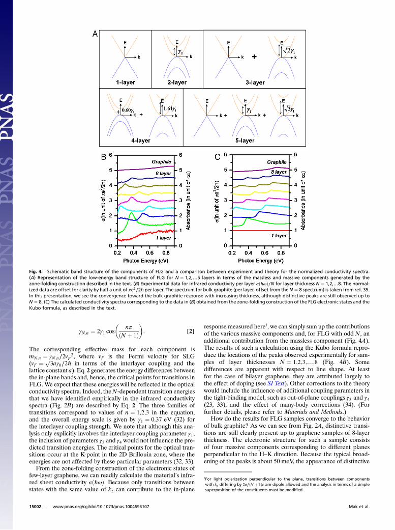
γN;n ¼ 2γ1 cos�
nπðN þ 1Þ
�: [2]
The corresponding effective mass for each component ismN;n ¼ γN;n∕2vF2, where vF is the Fermi velocity for SLG(vF ¼ p
3aγ0∕2ℏ in terms of the interlayer coupling and thelattice constant a). Eq. 2 generates the energy differences betweenthe in-plane bands and, hence, the critical points for transitions inFLG.We expect that these energies will be reflected in the opticalconductivity spectra. Indeed, theN-dependent transition energiesthat we have identified empirically in the infrared conductivityspectra (Fig. 2B) are described by Eq. 2. The three families oftransitions correspond to values of n ¼ 1;2;3 in the equation,and the overall energy scale is given by γ1 ¼ 0.37 eV (32) forthe interlayer coupling strength. We note that although this ana-lysis only explicitly involves the interlayer coupling parameter γ1,the inclusion of parameters γ3 and γ4 would not influence the pre-dicted transition energies. The critical points for the optical tran-sitions occur at the K-point in the 2D Brillouin zone, where theenergies are not affected by these particular parameters (32, 33).
From the zone-folding construction of the electronic states offew-layer graphene, we can readily calculate the material’s infra-red sheet conductivity σðℏωÞ. Because only transitions betweenstates with the same value of kz can contribute to the in-plane
response measured here†, we can simply sum up the contributionsof the various massive components and, for FLG with odd N, anadditional contribution from the massless component (Fig. 4A).The results of such a calculation using the Kubo formula repro-duce the locations of the peaks observed experimentally for sam-ples of layer thicknesses N ¼ 1;2;3;…;8 (Fig. 4B). Somedifferences are apparent with respect to line shape. At leastfor the case of bilayer graphene, they are attributed largely tothe effect of doping (see SI Text). Other corrections to the theorywould include the influence of additional coupling parameters inthe tight-binding model, such as out-of-plane couplings γ3 and γ4(23, 33), and the effect of many-body corrections (34). (Forfurther details, please refer to Materials and Methods.)
How do the results for FLG samples converge to the behaviorof bulk graphite? As we can see from Fig. 2A, distinctive transi-tions are still clearly present up to graphene samples of 8-layerthickness. The electronic structure for such a sample consistsof four massive components corresponding to different planesperpendicular to the H–K direction. Because the typical broad-ening of the peaks is about 50 meV, the appearance of distinctive
Fig. 4. Schematic band structure of the components of FLG and a comparison between experiment and theory for the normalized conductivity spectra.(A) Representation of the low-energy band structure of FLG for N ¼ 1;2;…5 layers in terms of the massless and massive components generated by thezone-folding construction described in the text. (B) Experimental data for infrared conductivity per layer σðℏωÞ∕N for layer thickness N ¼ 1;2;…8. The normal-ized data are offset for clarity by half a unit of πe2∕2h per layer. The spectrum for bulk graphite (per layer, offset from theN ¼ 8 spectrum) is taken from ref. 35.In this presentation, we see the convergence toward the bulk graphite response with increasing thickness, although distinctive peaks are still observed up toN ¼ 8. (C) The calculated conductivity spectra corresponding to the data in (B) obtained from the zone-folding construction of the FLG electronic states and theKubo formula, as described in the text.
†For light polarization perpendicular to the plane, transitions between componentswith kz differing by 2π∕ðN þ 1Þc are dipole allowed and the analysis in terms of a simplesuperposition of the constituents must be modified.
15002 ∣ www.pnas.org/cgi/doi/10.1073/pnas.1004595107 Mak et al.
features for 8-layer graphene is to be expected. We anticipate thatthe individual optical transitions arising from, say, more thantwenty subbands (i.e., N > 40 layers) would be blurred togetherand that response would become indistinguishable from thatof graphite. Indeed, we are able to reproduce the experimentaloptical conductivity for bulk graphite (35) by carrying out theKubo calculation for few-layer graphene with N ¼ 40 layers(Fig. 4 B and C). In this limit, although the peaks from individual2D interband transitions wash out, the absorption spectrumretains a broad maximum around 0.75 eV (Fig. 4C). Withinour description of FLG, this feature arises from the energy dis-tribution of the different 2D subband transitions in Eq. 2, whichshows that there are many transitions near the maximum energyof 2γ1. This results in a broad peak in the conductivity around thatenergy. The increased conductivity corresponds, in the languageof the bulk response, to the saddle-point singularity along theH–K direction in the 3D graphite band structure.
ConclusionsThe present work demonstrates that significant control of thelow-energy electronic states of graphene can be achieved byinterlayer interactions in few-layer samples. For each layer thick-ness N, carriers of differing masses are produced, with differingsplittings of the conduction and valence bands. For odd values ofthe layer thickness N, massless carriers are also present, as insingle-layer graphene. Understanding of the key features ofthe 2D band structure in N-layer graphene, and the associatedinfrared conductivity spectra, can be achieved on the basis of asimple and precisely defined zone folding of the 3D graphitebands. This situation is analogous to the standard descriptionof the 1D bands of single-walled carbon nanotubes in whichthe electronic structure of the panoply of different nanotubescan be generated by zone folding of the 2D electronic structureof graphene. Just as for carbon nanotubes, the additional controlof the electronic properties as a function structure for FLGshould extend the range of distinctive physical phenomena andapplications of this material system.
Materials and MethodsSample Preparation. We deposited FLG samples by mechanical exfoliation ofkish graphite (Toshiba) on high-purity SiO2 substrates (Chemglass, Inc.) thathad been carefully cleaning by sonication in methanol. The typical area ofthe FLG graphene samples was several hundreds to thousands of μm2. Weestablished the thickness of each of the deposited graphene samples usingabsorption spectroscopy in the visible spectral range, where each graphenelayer absorbs approximately 2.3% (26, 27, 36) of the light.
Reflectance Measurements. The infrared conductance measurements wereperformed using the NSLS at Brookhaven National Laboratory (U2B beam-line) as a bright source of broadband infrared radiation. We detected theoptical radiation reflected near normal incidence with a FTIR spectrometerequipped with a HgCdTe detector under nitrogen purge. The synchrotronradiation was focused to a spot size below 10 μm with a 32× reflectiveobjective. The reflectance spectra of the graphene samples were obtainedby normalizing the sample spectrum by that from the bare substrate, asin an earlier investigation of single-layer graphene (26). In that study, theeffects of finite beam divergence were also considered and shown to beinsignificant.
Conversion of the Measured Reflectance to the Infrared Conductivity σðℏωÞ. Fora sufficiently thin sample on a transparent substrate, its optical sheet conduc-tivity σðℏωÞ is related to the reflectance in a direct manner (26): The fractionalchange in reflectance associated with the presence of the thin-film sampleis proportional to the real part of its optical sheet conductivity σðℏωÞ, orequivalently, to its absorbance A ¼ ð4π∕cÞσðℏωÞ. We can therefore convert
the measured reflectance spectra into σðℏωÞ by multiplication of a suitablenumerical factor determined by the (frequency-dependent) refractive indexof the substrate (26). With increasing film thickness, propagation effectsbegin to play a role, and the relation between the conductivity (or dielectricfunction) of the film and themeasured properties becomes more complex. Todetermine the validity of the thin-film approximation in analysis of our data,we performed full calculations of the reflectance. Even for the thickest filmconsidered in our measurements, the 8-layer graphene sample, we did notsee significant changes in the shape of the inferred σðℏωÞ; errors in theinferredmagnitude of σðℏωÞwere limited to 15%. In the interest of simplicity,we consequently present all data based on the thin-film analysis.
Theoretical Basis for the Zone-Folding Scheme. In the text above, we consid-ered a TB Hamiltonian for N-layer graphene with arbitrary couplingsbetween atoms in the same or adjacent layers of graphene. In this model,the Bloch wavefunction is approximated as ψkðrÞ ¼ ∑ie
ikRϕðr − RiÞ, wherethe summation extends over all lattice sites Ri and ϕðrÞ represents the carbonpz orbital. In this treatment, we consider the structural properties of eachlayer in the sample (including the outer layers) as identical. This assumptionis reasonable for graphene, given the saturated character of its in-planebonds and the weakness of its out-of-plane interactions. Under theseassumptions, the eigenstates for N-layer graphene can be taken fromthose of the bulk graphite by constructing standing wave that satisfies theboundary condition of Eq. 1.
Influence of Other Interlayer Coupling Parameters. In our calculation of opticalconductivities using the Kubo formula, only a single in-plane interaction (γ0)and a single out-of-plane interaction (γ1) have been considered. In additionto the γ1 coupling, the dominant interactions for atoms in adjacent grapheneplanes are described by the parameters γ3 and γ4. Their inclusion has threeeffects on the band structure of FLG (13, 32): (i) They introduce overlaps(of a few meV) between the lower conduction and upper valence bands;(ii) they produce a weak asymmetry between the electron and hole masses;and (iii) they lead to trigonal warping for the dispersion away from theK-point of the 2D Brillouin zone. Effects (i) and (ii) do not alter the opticalconductivities, because the relevant energy scales are too small. For undopedor slightly doped FLG, effect (iii), controlled by coupling γ3, is also minor. Theabsorption features are dominated by transitions near the K-point where thejoint density of states is high. The inclusion of γ3 ≠ 0 will slightly modify theline shape of the optical transitions away from the critical points (23, 33).
We note that for an accurate description of the low-energy (∼10 meVscale) electronic bands and the Fermi surfaces of both FLG and bulk graphite,the couplings mentioned above must be considered. In addition, two furtherparameters are very important: the second-layer coupling strength γ2 and theA∕B sublattice asymmetry parameter Δ (10, 13, 32). The parameter γ2 intro-duces extra band overlaps (beyond the effect of γ3), andΔ ≠ 0 leads to a smallband gap for the 2D dispersion at the H point. The zone-folding scheme thatwe have successfully applied to describe the optical transitions of FLG interms of the properties of graphite can, however, be justified only whenall interactions beyond those of adjacent graphene layers can be neglected.Thus, the construction cannot be rigorously extended to include the case ofγ2 ≠ 0. The zone-folding procedure has, correspondingly, limited validityfor predicting the details of the Fermi surfaces in FLG, which will generallydepend sensitively on the details of the low-energy band structure ofgraphite. For further discussion of the nature of the low-energy bandsand Fermi surfaces of FLG, we refer the reader to the literature (10, 13).
ACKNOWLEDGMENTS. We thank Drs. Mikito Koshino, Mark S. Hybertsen, andSami Rosenblatt for valuable discussions. The authors at Columbia Universityacknowledge support from the Nanoscale Science and Engineering Initiativeof the National Science Foundation under Grant CHE-06-41523, from theNew York State Office of Science, Technology, and Academic Research(NYSTAR), and from the Office of Naval Research under the MultidisciplinaryUniversity Research Initiative (MURI) program; the authors at Brookhavenwere supported under contract DE-AC02-98CH10886 with the US Depart-ment of Energy. The synchrotron studies were supported by the NSLS atBrookhaven and the Center for Synchrotron Biosciences, Case WesternReserve University, under P41-EB-01979 with the National Institute forBiomedical Imaging and Bioengineering.
1. Geim AK (2009) Graphene: Status and prospects. Science 324:1530–1534.
2. Ohta T, Bostwick A, Seyller T, Horn K, Rotenberg E (2006) Controlling the electronic
structure of bilayer graphene. Science 313:951–954.
3. McCann E (2006) Asymmetry gap in the electronic band structure of bilayer graphene.
Phys Rev B 74:161403(R)-1–161403(R)-4.
4. Castro EV, et al. (2007) Biased bilayer graphene: Semiconductor with a gap tunable bythe electric field effect. Phys Rev Lett 99:216802-1–216802-4.
5. Oostinga JB, Heersche HB, Liu XL, Morpurgo AF, Vandersypen LMK (2008)Gate-induced insulating state in bilayer graphene devices. Nat Mater 7:151–157.
6. Yao W, Xiao D, Niu Q (2008) Valley-dependent optoelectronics from inversionsymmetry breaking. Phys Rev B 77:235406-1–235406-7.
Mak et al. PNAS ∣ August 24, 2010 ∣ vol. 107 ∣ no. 34 ∣ 15003
PHYS
ICS

7. McCann E, Fal’ko VI (2006) Landau-level degeneracy and quantum Hall effect in agraphite bilayer. Phys Rev Lett 96:086805-1–086805-4.
8. Guinea F, Castro Neto AH, Peres NMR (2006) Electronic states and Landau levels ingraphene stacks. Phys Rev B 73:245426-1–245426-8.
9. Latil S, Henrard L (2006) Charge carriers in few-layer graphene films. Phys Rev Lett97:036803-1–036803-4.
10. Partoens B, Peeters FM (2006) From graphene to graphite: electronic structure aroundthe K point. Phys Rev B 74:075404-1–075404-11.
11. Manes JL, Guinea F, Vozmediano MAH (2007) Existence and topological stability ofFermi points in multilayered graphene. Phys Rev B 75:155424-1–155424-6.
12. Koshino M, Ando T (2007) Orbital diamagnetism in multilayer graphenes: Systematicstudy with the effective mass approximation. Phys Rev B 76:085425-1–085425-11.
13. Gruneis A, et al. (2008) Tight-binding description of the quasiparticle dispersion ofgraphite and few-layer graphene. Phys Rev B 78:205425-1–205425-16.
14. Min HK, MacDonald AH (2008) Chiral decomposition in the electronic structure ofgraphene multilayers. Phys Rev B 77:155416-1–155416-5.
15. Min HK, MacDonald AH (2009) Origin of universal optical conductivity andoptical stacking sequence identification in multilayer graphene. Phys Rev Lett103:067402-1–067402-4.
16. Castro Neto AH, Guinea F, Peres NMR, Novoselov KS, Geim AK (2009) The electronicproperties of graphene. Rev Mod Phys 81:109–162.
17. Katkov VL, Osipov VA (2009) Energy distributions of field emitted electrons fromcarbon nanosheets: Manifestation of the quantum size effect. JETP Lett 90:278–283.
18. Wang F, et al. (2008) Gate-variable optical transitions in graphene. Science320:206–209.
19. Li ZQ, et al. (2009) Band structure asymmetry of bilayer graphene revealed by infraredspectroscopy. Phys Rev Lett 102:037403-1–037403-4.
20. Zhang Y, et al. (2009) Direct observation of a widely tunable bandgap in bilayergraphene. Nature 459:820–823.
21. Mak KF, Lui CH, Shan J, Heinz TF (2009) Observation of an electric-field-induced band gap in bilayer graphene by infrared spectroscopy. Phys Rev Lett102:256405-1–256405-4.
22. Kuzmenko AB, et al. (2009) Infrared spectroscopy of electronic bands in bilayergraphene. Phys Rev B 79:115441-1–115441-5.
23. Kuzmenko AB, Crassee I, van der Marel D, Blake P, Novoselov KS (2009) Determinationof the gate-tunable band gap and tight-binding parameters in bilayer graphene usinginfrared spectroscopy. Phys Rev B 80:165406-1–165406-12.
24. Seyller Th, et al. (2008) Epitaxial graphene: A new material. Phys Status Solidi B 245:1436–1446.
25. Saito R, Dresselhaus G, DresselhausMS (1998) Physical Properties of Carbon Nanotubes(Imperial College Press, London).
26. Mak KF, et al. (2008) Measurement of the optical conductivity of graphene. Phys RevLett 101:196405-1–196405-4.
27. Nair RR, et al. (2008) Fine structure constant defines visual transparency of graphene.Science 320:1308.
28. Ando T, Zheng YS, Suzuura H (2002) Dynamical conductivity and zero-mode anomalyin honeycomb lattices. J Phys Soc Jpn 71:1318–1324.
29. Abergel DSL, Fal’ko VI (2007) Optical and magneto-optical far-infrared properties ofbilayer graphene. Phys Rev B 75:155430-1–155430-5.
30. Koshino M, Ando T (2008) Magneto-optical properties of multilayer graphene. PhysRev B 77:115313-1–115313-8.
31. Mak KF, Shan J, Heinz TF (2010) Electronic structure of few-layer graphene:Experimental demonstration of strong dependence on stacking sequence. Phys RevLett 104:176404-1–176404-4.
32. Dresselhaus MS, Dresselhaus G (1981) Intercalation compounds of graphite. Adv Phys30:139–326.
33. Zhang LM, et al. (2008) Determination of the electronic structure of bilayer graphenefrom infrared spectroscopy. Phys Rev B 78:235408-1–235408-11.
34. Yang L, Deslippe J, Park CH, CohenML, Louie SG (2009) Excitonic effects on the opticalresponse of graphene and bilayer graphene. Phys Rev Lett 103:186802-1–186802-4.
35. Taft EA, Philipp HR (1965) Optical properties of graphite. Phys Rev 138:A197–A202.36. Gaskell PE, Skulason HS, Rodenchuk C, Szkopek T (2009) Counting graphene layers on
glass via optical reflection microscopy. Appl Phys Lett 94:143101-1–143101-3.
15004 ∣ www.pnas.org/cgi/doi/10.1073/pnas.1004595107 Mak et al.
![Microscale study of frictional properties of graphene in ... · on epitaxially grown graphene [22]. We show that unlike bulk graphite, few-layer graphene can result in a significant](https://static.fdocuments.in/doc/165x107/5f1708e078420743e77f202c/microscale-study-of-frictional-properties-of-graphene-in-on-epitaxially-grown.jpg)