The Erlangen Slot Machine An FPGA-Based Partially … Erlangen Slot Machine An FPGA-Based Partially...
177
Transcript of The Erlangen Slot Machine An FPGA-Based Partially … Erlangen Slot Machine An FPGA-Based Partially...

The Erlangen Slot Machine � An
FPGA-Based Partially
Recon�gurable Computer
Der Technischen Fakultät der
Universität Erlangen-Nürnberg
zur Erlangung des Grades
D O K T O R - I N G E N I E U R
vorgelegt von
Mateusz Majer
Erlangen 2011


Als Dissertation genehmigt vonder Technischen Fakultät derUniversität Erlangen-Nürnberg
Tag der Einreichung: 19.10.2010Tag der Promotion: 20.01.2011Dekan: Prof. Dr.-Ing. Reinhard GermanBerichterstatter: Prof. Dr.-Ing. Jürgen Teich
Prof. Dr. Dr. h.c. mult. Manfred Glesner
3

4

Abstract
Partial recon�guration is a special case of device con�guration that allows to
change only parts of a hardware circuit at run-time. Only a prede�ned region
of an FPGA is updated while the remainder of the device continues to operate
undisturbed. This is especially valuable when a device operates in a mission-
critical environment and cannot be disrupted while a subsystem is rede�ned
for performance or �exibility reasons. The triggering of partial recon�guration
can be instigated by user requests, detected changes of environmental factors
or operating system scheduling. It o�ers a novel possibility to dynamically load
and execute hardware modules, previously only known for software modules.
Partial recon�guration is useful in increasing the computational �exibility and
e�ciency by time-sharing the existing memory and logic resources on the device.
Using partial recon�guration, the functionality of a single FPGA is increased,
allowing fewer or smaller FPGA devices to be used. Embedded systems using
FPGAs supporting partial recon�guration can be customized in their hardware
at run-time with partial recon�guration. However, the design �ow and pe-
ripheral I/O architectures of these devices are not ideally suited for run-time
recon�gurable application development. Therefore, the bene�ts of partial re-
con�guration used in hardware designs are currently seen as limited.
The Erlangen Slot Machine (ESM) is introduced as a new FPGA-based dynam-
ically recon�gurable computer architecture supporting run-time customization
through the use of partial recon�guration at its architectural level. Built within
the DFG priority program 1148 Recon�gurable Computing its main goals are:
• making partial recon�gurable designs viable for real-world applications,
5

• operating system support for scheduling, placement and run-time recon-
�guration of partially recon�gurable modules,
• tool support for the development of run-time recon�gurable computation
and communication modules using new inter-module communication para-
digms, and to
• provide a platform for interdisciplinary research on algorithms, methods,
and applications using run-time recon�guration.
Its architectural support for partial recon�gurable modules simpli�es the design
and evaluation of modular and partially recon�gurable applications. Its key
bene�t is the decoupling of all peripheral I/O pins from the FPGA through
the use of an external crossbar. This feature enables �exible signal routing to
any recon�gurable region on the FPGA and e�ectively decouples the peripheral
I/Os from the �xed FPGA pins. Moreover, it provides a �exible platform for
run-time allocation models, real-time aspects and operating systems research
for run-time recon�gurable systems.
The design �ow tool SlotComposer automates the creation of partially recon-
�guration modules. It allows the automated insertion of inter-module commu-
nication structures. Moreover, it aids partial module placement with graphical
visualization and creates design �ow scripts for partial bitstream synthesis.
As an application example using partial run-time recon�guration, an advanced
video application was implemented on the ESM platform. To support real-time
video processing in the application, methods for hardware-software communi-
cation, hardware task placement, inter-module communication and decoupled
peripheral I/O access were analyzed and implemented for use on the ESM plat-
form.
6
Deutscher Titel und
Zusammenfassung
Die Erlangen Slot Machine � Einepartiell rekon�gurierbare FPGA-basierte
Computerarchitektur
Kurzzusammenfassung
Partielle Rekon�guration ist ein Spezialfall der FPGA-Kon�guration, bei der
zur Laufzeit eine vorde�nierte FPGA-Region mit einer neuen Schaltung geladen
wird, während dabei die übrigen Regionen des FPGAs nicht gestört werden. Dies
ist besonders erwünscht, wenn Geräte in einer kritischen Umgebungen arbeiten
und ihr laufender Betrieb nicht unterbrochen werden darf. In diesem Fall erlaubt
die partielle Rekon�guration die Schaltungen von Teilsystemen im laufenden
Betrieb auszutauschen, um die E�zienz und die Flexibilität der Schaltung, auf-
grund von wechselnden Anforderungen oder variierenden Umgebungsfaktoren,
zu verbessern.
7

Die Verwendung der partiellen Rekon�guration erhöht die Funktionalität und
Flexibilität eines einzelnen FPGAs, so dass kleinere und somit günstigere FPGA-
Bausteine verwendet werden können. Eingebettete Systeme mit FPGAs könnten
damit im laufenden Betrieb an sich wechselnde Anforderungen in Echtzeit ange-
passt werden, wodurch die Implementierung verschiedener Anforderungen in ei-
nem einzigen Baustein zusammengelegt werden kann. Allerdings haben verschie-
dene Module unterschiedliche Anforderungen an die I/O- und Speicherschnitt-
stellen, welche von aktuellen FPGA-Plattformen nicht berücksichtigt werden
und damit die Entwicklung von rekon�gurierbaren Anwendungen erschweren.
Diese Einschränkungen haben dazu geführt, dass im Bereich der partiellen Re-
kon�guration nur wenige Beispiele die praktische Anwendbarkeit der partiellen
Rekon�guration zeigen.
Die Erlangen Slot Machine (ESM) ist eine neuartige FPGA-basierte, dynamisch
rekon�gurierbare Computerarchitektur, die für den Einsatz von partieller Re-
kon�guration konsequent ausgelegt wurde. Ihre �exible Architektur vereinfacht
die Entwicklung und Evaluierung von modularen und partiell rekon�gurierbaren
Hardware-Designs. Ihr groÿer Vorteil ist die Entkopplung aller peripheren I/O-
Pins durch den Einsatz einer externen Crossbar. Diese ermöglicht eine �exible
Signalverteilung zu jeder rekon�gurierbaren Region auf dem FPGA, wodurch die
peripheren I/Os von den physikalischen FPGA-Pins entkoppelt werden. Darüber
hinaus bietet die ESM eine �exible Plattform für Entwicklung und Analyse von
Scheduling, Platzierungsverfahren und Echtzeitbetriebssystemen für laufzeitre-
kon�gurierbare FPGA-Systeme im Allgemeinen.
Mit dem Design-FlowWerkzeug SlotComposer wird die automatische Erstellung
von partiell rekon�gurierbaren Modulen verwirklicht. Es ermöglicht das auto-
matisierte Einfügen von Kommunikationsverbindungen zwischen partiellen Mo-
dulen, die graphische Platzierung von partiellen Modulen, als auch das Erstellen
von Design-Flow Skripten für die Kon�gurationsdaten-Synthese der partiellen
Module.
Als Anwendungsbeispiel für die partielle Rekon�guration wurde eine erweiterte
Video-Anwendung, die ein Assistenzsystem für die Erkennung von vorausfahren-
den Fahrzeugen und Fahrbahnmarkierungen, auf der ESM-Plattform vollstän-
dig implementiert. Zur Unterstützung der Echtzeit-Videoverarbeitung mit par-
tiell rekon�gurierbaren Video�ltern wurden Methoden für Hardware-Software-
Kommunikation, Modul-Platzierung, Inter-Modul Kommunikation sowie Zugri�
auf die I/O Pins der Peripherieschnittstellen entwickelt.
8

Acknowledgments
First and foremost, I would not have begun nor been able to complete this work
without the love, support, and encouragement of my partner Meline, my family
and my friends. Without them, this dissertation would not have been possible.
Moreover, I am indebted to my PhD adviser Prof. Jürgen Teich for support-
ing this exciting course of research and for advising on this dissertation. His
vision, enthusiasm, and expertise motivated me as much as I bene�ted from
his open support for the Erlangen Slot Machine endeavor. Thanks to my ex-
ternal committee members Prof. Manfred Glesner, Prof. Robert Weigel, and
Prof. Wolfgang Schröder-Preikschat. Moreover, special thanks go to Prof. Sán-
dor Fekete and Jan van der Veen for their assistance and great collaboration on
the conceptual part of the Erlangen Slot Machine and algorithmic part of the
ReCoNodes project.
I have had a great deal of assistance from the sta�, students and visitors to the
Department of Computer Science 12. In particular, I thank Hritam Dutta, Josef
Angermeier, Ali Ahmadinia, Christophe Bobda, Jan van der Veen, Dirk Koch
and Thilo Streichert for reviewing, discussing and helping me to clarify many
aspects of this work. Big thanks go also to Ulrich Batzer, Matthias Kovatsch,
Jan Grembler,André Linarth and Thomas Haller, without whom my work would
not exist in this form.
Furthermore, this work was supported by DFG grant TE 163/14-2, project Re-
CoNodes [1, 2], funded within the priority program 1148, Recon�gurable Com-
puting Systems [3]. I would also like to acknowledge the DFG for providing
9
additional support to build 20 prototypes of the ESM boards. And a special
thanks goes to Patrick Lysaght at Xilinx for his great support.
As the development of the Erlangen Slot Machine platform [4] was a huge task,
it would have been impossible without joint work on di�erent �elds:
Ulrich Batzer Taillight recognition demonstrator [5]Matthias Kovatsch Taillight recognition demonstrator [6]Bruno Kleinert Recon�guration manager driver [7]Thomas Stark Crossbar software driver [8]Plamen Shterev SlotComposer design �ow [9]Jan Grembler Video demonstrator [10]Christian Freiberger Recon�guration manager [11]Felix Reimann RMB communication [12]Peter Asemann PowerPC board support package [13]André Linarth ESM Motherboard [14]Thomas Haller ESM Babyboard [15]
I feel indebted to all persons involved in this great project and would like to
thank them again for their great work.
Mateusz Majer
München, July 2010
10

Contents
Abstract 5
Deutscher Titel und Zusammenfassung 7
Acknowledgments 9
1. Introduction 15
1.1. Motivation . . . . . . . . . . . . . . . . . . . . . . . . . . . . . . 19
1.2. Contributions . . . . . . . . . . . . . . . . . . . . . . . . . . . . 23
1.3. Overview . . . . . . . . . . . . . . . . . . . . . . . . . . . . . . 25
2. Background 27
2.1. What is Recon�gurable Computing? . . . . . . . . . . . . . . . 27
2.2. Recon�gurable Hardware . . . . . . . . . . . . . . . . . . . . . . 28
2.2.1. Fine-Grained Architectures . . . . . . . . . . . . . . . . 29
2.2.2. Coarse-Grained Architectures . . . . . . . . . . . . . . . 36
2.2.3. Con�gurable Processors . . . . . . . . . . . . . . . . . . 38
2.2.4. Related Computing Platforms . . . . . . . . . . . . . . . 39
2.3. Partial Recon�guration . . . . . . . . . . . . . . . . . . . . . . . 39
2.4. Technical Advantages and Limitations . . . . . . . . . . . . . . 41
3. The Erlangen Slot Machine 45
3.1. Introduction . . . . . . . . . . . . . . . . . . . . . . . . . . . . . 45
3.2. Communication Models . . . . . . . . . . . . . . . . . . . . . . . 48
3.3. Implemented Architecture . . . . . . . . . . . . . . . . . . . . . 52
3.4. The Babyboard . . . . . . . . . . . . . . . . . . . . . . . . . . . 56
3.4.1. Main FPGA . . . . . . . . . . . . . . . . . . . . . . . . . 59
3.4.2. The Recon�guration Manager . . . . . . . . . . . . . . . 60
3.5. The Motherboard . . . . . . . . . . . . . . . . . . . . . . . . . . 67
3.5.1. PowerPC . . . . . . . . . . . . . . . . . . . . . . . . . . 69
3.5.2. Crossbar . . . . . . . . . . . . . . . . . . . . . . . . . . . 70
11

Contents
3.5.3. Video Input . . . . . . . . . . . . . . . . . . . . . . . . . 74
3.5.4. Video Output . . . . . . . . . . . . . . . . . . . . . . . . 75
4. Development of Partially Recon�gurable Modules 77
4.1. Introduction . . . . . . . . . . . . . . . . . . . . . . . . . . . . . 77
4.2. Partial Design Flow . . . . . . . . . . . . . . . . . . . . . . . . . 79
4.3. The SlotComposer . . . . . . . . . . . . . . . . . . . . . . . . . 83
4.4. Operating System Framework . . . . . . . . . . . . . . . . . . . 86
4.5. Real-time Recon�gurable Hardware Task Management . . . . . 90
4.5.1. Hardware Task Generation . . . . . . . . . . . . . . . . . 94
4.5.2. Design Flow . . . . . . . . . . . . . . . . . . . . . . . . . 95
4.6. Hardware Interfaces for Video Processing . . . . . . . . . . . . . 101
4.6.1. Overview . . . . . . . . . . . . . . . . . . . . . . . . . . 101
4.6.2. HW/SW Communication . . . . . . . . . . . . . . . . . . 103
4.6.3. Video Input . . . . . . . . . . . . . . . . . . . . . . . . . 103
4.6.4. Video Output . . . . . . . . . . . . . . . . . . . . . . . . 104
4.6.5. Memory Interfaces . . . . . . . . . . . . . . . . . . . . . 104
5. Application Scenarios and Use Cases 107
5.1. Introduction . . . . . . . . . . . . . . . . . . . . . . . . . . . . . 107
5.2. Real-Time Video Processing on the ESM . . . . . . . . . . . . . 109
5.2.1. Data Flow . . . . . . . . . . . . . . . . . . . . . . . . . . 109
5.2.2. Main FPGA Partitioning . . . . . . . . . . . . . . . . . . 111
5.3. Implemented Video-Engines . . . . . . . . . . . . . . . . . . . . 112
5.3.1. Basic Video Filters . . . . . . . . . . . . . . . . . . . . . 112
5.3.2. Edge-Engine . . . . . . . . . . . . . . . . . . . . . . . . . 115
5.3.3. Taillight-Engine . . . . . . . . . . . . . . . . . . . . . . . 116
5.4. A Point-Based Rendering Application . . . . . . . . . . . . . . . 124
5.4.1. Background . . . . . . . . . . . . . . . . . . . . . . . . . 125
5.4.2. Rendering Pipeline . . . . . . . . . . . . . . . . . . . . . 128
5.4.3. Implementation Results . . . . . . . . . . . . . . . . . . 133
6. Conclusions 137
6.1. Summary of Contributions . . . . . . . . . . . . . . . . . . . . . 137
6.2. Interdisciplinary Research Platform . . . . . . . . . . . . . . . . 140
6.3. Future Work . . . . . . . . . . . . . . . . . . . . . . . . . . . . 142
A. Glossary 145
12

Contents
B. Technical Speci�cation of the ESM 149
List of Figures 149
List of Tables 156
Bibliography 157
Curriculum Vitae 177
13

Contents
14

1. Introduction
Over the years, embedded systems designers have used di�erent approaches to
design systems in ways that optimize and customize hardware to �t the speci�c
requirements of the application they are developing. These approaches fall into
software, recon�gurable hardware and user-speci�ed hardware categories.
Recon�gurable hardware devices are hardware devices in which the functionality
of the logic gates is customizable at run-time. The connections between the logic
gates are also con�gurable. Memories are used as look-up tables to implement
the universal gates, and are used to control the con�guration of the switches in
the interconnection network. The program that indicates the functionality of
each gate and the switch state is called a con�guration.
Field-Programmable Gate Arrays (FPGAs) are the most common type of re-
con�gurable hardware devices. Their functionality is set at power-up and can
be changed during run-time.
User-speci�ed hardware is used to create custom physical silicon to implement
the target device. This ranges from a minimal e�ort such as a gate array to a
fully-customized device with handcrafted features, known as Application Speci�c
Integrated Circuits (ASICs). Their functionality is set during manufacturing
and is immutable. However, the long development process, very high setup
costs preposition this approach for high volume applications only.
One currently new approach for compute intensive applications is stream com-
puting. It uses parallel software programming languages, that target massively
parallel processor arrays, such as Graphics Processing Units (GPUs). How-
ever, this approach is currently not suited for embedded applications because
15

1. Introduction
its power consumption of more than 100 Watts is too high for most embedded
systems [16, 17].
Applications implemented in hardware devices display e�ciency in concurrent
applications, achieved by using multiple parallel processing blocks. Coupled
with their �exibility to allow the embedded systems designer to tailor the device
to match their application's demands as closely as possible, hardware devices
achieve the highest possible throughput. The per-block power of an FPGA may
now be well be below that of DSPs, even though the chip-level power dissipation
is higher. DSPs typically consume 3-4 Watt and FPGAs 7-10 Watt but FPGAs
can often handle 10x the processing load by using multiple parallel processing
blocks [18].
Recon�gurable Computing (RC) has started with the advent of FPGAs and
hardware-oriented design languages like VHDL and Verilog. They enable a
10x to 100x gain over a conventional microprocessor in performance and func-
tional density (operations per area-time) [18]. The advantage of recon�gurable
computing comes from highly parallel data paths and post production pro-
grammability which allows data �ows to be highly specialized to the applica-
tion. Moreover, partial dynamic recon�guration enables run-time specialization
which brings about software like �exibility to the hardware domain.
Recon�gurable architectures can re-adapt the behavior of their hardware re-
sources to a speci�c computation that needs to be performed. Computing using
recon�gurable architectures provides an alternate paradigm to utilize available
logic resources on the chip analog to software multithreading. However, the
performance gains obtained by the use of recon�gurable devices are limited
as development complexity and system integration costs increase. Moreover,
programming hardware devices remains di�cult, usually requiring a hardware-
oriented language such as Verilog or VHDL. Hardware solutions can take an
order of magnitude longer to code and verify than software solutions which im-
pacts development costs and increases time to market. New high-level languages
like Impulse-C or Mitron-C can shorten the development time, but they need
further development to match VHDL's e�ciency [19].
All user-programmable features inside an FPGA are controlled by memory cells
that are volatile and, therefore, must be con�gured on power-up. These memory
cells are known as the con�guration memory, and de�ne the Look-Up Tables
(LUT) , signal routing, Input/Output Blocks' (IOBs) voltage standards, and all
16
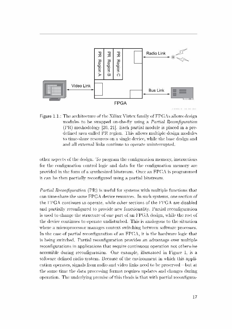
Figure 1.1.: The architecture of the Xilinx Virtex family of FPGAs allows designmodules to be swapped on-the-�y using a Partial Recon�guration(PR) methodology [20, 21]. Each partial module is placed in a pre-de�ned area called PR region. This allows multiple design modulesto time-share resources on a single device, while the base design andand all external links continue to operate uninterrupted.
other aspects of the design. To program the con�guration memory, instructions
for the con�guration control logic and data for the con�guration memory are
provided in the form of a synthesized bitstream. Once an FPGA is programmed
it can be then partially recon�gured using a partial bitstream.
Partial Recon�guration (PR) is useful for systems with multiple functions that
can time-share the same FPGA device resources. In such systems, one section of
the FPGA continues to operate, while other sections of the FPGA are disabled
and partially recon�gured to provide new functionality. Partial recon�guration
is used to change the structure of one part of an FPGA design, while the rest of
the device continues to operate undisturbed. This is analogous to the situation
where a microprocessor manages context switching between software processes.
In the case of partial recon�guration of an FPGA, it is the hardware logic that
is being switched. Partial recon�guration provides an advantage over multiple
recon�gurations in applications that require continuous operation not otherwise
accessible during recon�guration. One example, illustrated in Figure 1, is a
software de�ned radio system. Because of the environment in which this appli-
cation operates, signals from radio and video links need to be preserved � but at
the same time the data processing format requires updates and changes during
operation. The underlying premise of this thesis is that with partial recon�gura-
17

1. Introduction
tion, the system can maintain these real-time links while other modules within
the FPGA are changed on-the-�y [20, 21].
The recon�guration process can be classi�ed whether only the whole device is
programmed as one entity only once (static full recon�guration), or whether
just parts of the device are recon�gured at run-time (partial recon�guration).
Before an FPGA is operational after recon�guration, a certain time elapses,
often called recon�guration time. These di�erent terms of recon�guration are
illustrated inf Figure 1. The partial recon�guration of individual slots achieves
a higher �exibility and reduces recon�guration times (gray areas).
A
A1 A2 A1 A2
M6 M5 M7
M8 M5 M9 M10
M1 M3
M4 M5
M2 M1 M2
timea)
b)
c)
Slot 6
Slot 5
Slot 4
Slot 3
Slot 2
Slot 1
Slot 6
Slot 5
Slot 4
Slot 3
Slot 2
Slot 1
Slot 6
Slot 5
Slot 4
Slot 3
Slot 2
Slot 1
Run-time full reconfiguration
Run-time partial reconfiguration
Static full reconfiguration
Reconfiguration time Execution time
time
time
Figure 1.2.: Di�erent recon�guration modes supported by the ESM platform: a)static full recon�guration, b) run-time full recon�guration, and c)run-time partial recon�guration.
18
1.1. Motivation
1.1. Motivation
Despite the announcement made by several companies in the last couple of years
about the design and production of new and mostly coarse-grained recon�g-
urable chips [22, 23, 24], the dominant part of today's recon�gurable computing
platforms are still �ne-grained and FPGA-based.
The growing capacities provided by FPGAs as well as their partial recon�g-
uration capabilities allow them to implement complex digital designs. Xilinx
FPGAs [25, 26, 27, 28] combine the advantages of large capacity and the ability
to support partial recon�guration. The Virtex-II series o�ers enough logic for
e�ciently implementing applications with high demand of resources, e.g., arising
in video, audio and signal processing as well as in other �elds like automotive
applications.
There are, however, open problems concerning module relocation: In order to
connect a module to other modules and/or pins, signals are often required to
pass through other modules. Those signals used by a given module and crossing
other modules are called feed-through signals. Using feed-through lines to access
resources has, however, two negative consequences, as illustrated in Figure 1.3:
• Di�culty of design automation: Each module must be implemented with
all possible feed-through channels needed by other modules. Because de-
signers only know at run-time which module needs to feed through a signal,
many channels reserved for a possible feed-through become redundant.
• Relocation of modules: Modules accessing external pins are no longer
relocatable, because they are compiled for �xed locations where a direct
signal line to these pins is established.
Many FPGA-based recon�gurable platforms such as [29, 30, 31, 32] o�er vari-
ous interfaces for audio, video capturing and rendering and for communication.
However, each interface is connected to the FPGA using dedicated pins at �xed
locations. Modules with access to a given interface such as a VGA input port
must be placed in the area of the chip where the FPGA signals are connected.
If the input or output signals are not grouped together then the relocation of
these modules becomes impossible. Until now, no platform on the market has
provided a solution to these problems.
19

1. Introduction
Figure 1.3.: The feed-through line problem with relocatable modules. Placing anew module B into slot two requires that the new module provides allfeed-through lines needed by slot one and three. This fact disablesany module relocation and makes it impossible to place moduleswith di�erent feed-through requirements into the other slots.
The most important problems limiting the use of partial and dynamic recon�g-
uration are:
• limited support for partial recon�guration,
• I/O-pin dilemma,
• inter-module communication dilemma and
• local memory dilemma.
These limits of existing FPGA-based recon�gurable computers are explained in
detail in Section 3.4:
Very few FPGAs allowing partial recon�guration exist on the market. These
few FPGAs, like the Virtex series by Xilinx [25], impose nonetheless some re-
strictions on the least amount of resources that can be recon�gured at a time,
for example column-wise recon�guration.
Many existing platforms include I/O peripherals like video, RAMs, audio, ADC
(analog to digital converter) and DAC (digital to analog converter) connected at
�xed pins of the FPGA device. As a consequence of these pin constraints, partial
recon�guration may be di�cult or even impossible, because a new module can
20

1.1. Motivation
require access to di�erent I/O pins. Another problem related to pins is that
the pins belonging to a given logical group like video, and audio interfaces are
not situated closely to each other. On many platforms, they are spread around
the device. A module accessing an external device will have to feed many lines
through many di�erent components. This situation is illustrated in Figure 1.4:
Two modules (one of which is a VGA module) are implemented. The VGA
module uses a large number of pins at the bottom part of the device and also
on the right hand side. Implementing a module without feed-through lines is
only possible on the two �rst columns on the left hand side. The e�ort needed
for implementing a recon�gurable module on more than two columns together
with the VGA module is very high. FPGA development boards from Celoxica
Ltd. [29], Alpha Data Ltd. [30], XESS Corp. , and Nallatech Inc. all exhibit the
same limitations. On the XF-Board [33, 32] from ETH Zurich, the peripherals
are connected to one side of the device. Each module accesses I/Os through an
operating system (OS) layer implemented on the left and right part of the device.
Many other existing platforms like the RAPTOR board [34], Celoxica RC1000
and RC2000 [29] are PCI systems that require a workstation for operation. The
use in stand-alone systems as needed in many embedded systems is not possible.
Modules placed at run-time on the device typically need to exchange data among
each other. Such a request for communication is dynamic due to run-time mod-
ule placement. Dynamically routing signal lines on the hardware is a very cum-
bersome task. For e�ciency reasons, new communications paradigms must be
investigated to support such dynamic connection requests, for example packet-
based DyNoCs [35] or principles of self-circuit routing.
Modules requiring large amounts of local memory cannot be implemented since
a module can only occupy the memory inside its physical slot boundary. Stor-
ing data in o�-chip memories is therefore the only solution. However, existing
FPGA-based platforms often have only one or two external memory banks and
their pin connections are spread over the borders of the FPGA.
The design and implementation of a recon�gurable computing platform poses
many challenging problems. Motivation to research these challenging problems
is re�ected in the following topics and tasks, especially through related an rele-
vant research questions:
Hardware Support How should the hardware device be partitioned so that
multiple independent tasks can execute? Can multiple I/O streams be
21

1. Introduction
Figure 1.4.: Pin distribution of a VGA module on the RC200 platform. It can beseen that the VGA Module occupies pins on the bottom and rightFPGA borders. In consequence, only a narrow part on the left sideis available for dynamic module recon�guration.
supported? How hard is it to access external memory? How is con�gura-
tion data manged and who is controlling the recon�guration process?
Task Design Each task has to communicate with external I/Os or with other
running tasks. How does the task development process support inter-
module and external communication? What are global requirements for
supporting arbitrary task placement? How should relocatable tasks be
designed so they do not interfere with neighboring tasks? How can tools
automate the development process?
OS Framework Basic operating system services are needed for run-time schedul-
ing and placement. How can the overhead of the operating system be
minimized? Should the operating system itself be a hardware task or run
on a separate microprocessor? Additionally, the lack of advanced software
tools is a signi�cant bottleneck in application development with partial
recon�guration support.
To support parallel execution of hardware tasks analog to software multitask-
ing a well de�ned methodology for the development of these tasks has to be
established. At the operating system level hardware resources, caching of con-
�guration data for each hardware task, access to global memory and communi-
cation resources must be e�ciently manged. These challenging problems gen-
erate many questions that need to be solved in order to enable the creation of
a �exible recon�gurable platform, as illustrated in Figure 1.5. The operating
22

1.2. Contributions
system manages the recon�gurable hardware by providing an abstraction layer
between task request and the recon�gurable hardware device as illustrated in
Figure. Each task request fetches the corresponding module con�guration from
a module database. The scheduler determines the exact point in time for the
module to be loaded into the hardware device [36]. However, this can only be
performed if the placer can �nd a free region that the module can �t in. More-
over, the number of free regions can be further limited through defragmenting
of the device area which is caused by frequent loading of new modules [37].
Based on the above review of current platform capabilities, issues, and questions,
this thesis contends that the present underuse of partial dynamic recon�guration
is due in great part to a lack of a standardized development environment and
a common operating system framework platform to support its key technology
bene�ts.
Figure 1.5.: Overview of a recon�gurable computing platform. The recon�g-urable hardware device is controlled by an operating system whichloads partial tasks on request.
1.2. Contributions
The Erlangen Slot Machine, a new FPGA-based partially recon�gurable plat-
form, overcomes the I/O bottleneck of existing FPGA-based platforms by imple-
menting a crossbar oriented peripheral I/O architecture and dedicated external
23

1. Introduction
memory for up to six partial modules [38, 39, 40, 41, 42]. This recon�gurable
platform also includes an external processor for main control and a dedicated
FPGA for recon�guration management [43]. These architectural features o�-
load partial recon�guration support and management functions form the main
FPGA to external devices [44]. This enables the sole use of the main FPGA for
partial recon�gurable modules. Another resulting feature is a simpli�ed devel-
opment process as static control logic does not intervene with the development
of run-time recon�gurable tasks. Thus, up to 22 partial hardware tasks can be
loaded on demand while satisfying peripheral I/O access of each partial task
through the external crossbar [45].
Also new is the introduction of a tool support for an automated transformation
of hardware designs into partial hardware designs at the HDL-level. When a
part of an application is moved to a partial hardware module, the design �ow
was found to be very time consuming and error prone because a new top-level
module with intermediate communication modules and signals had to be cre-
ated. Therefore, a software tool called SlotComposer was developed to generate
communication glue logic needed for partial recon�guration at the top HDL-
level. The use of platform tailored communication schemes further reduces the
development time [46, 47].
The complexity of implementing a fully working video application on an FPGA
is high, especially if external memories and peripheral I/Os are used. To prove
the ESM concept's practicability for complex applications using partial recon-
�guration, a video processing application for lane and object detection for a
driver assistance system was successfully implemented [48, 49]. This applica-
tion utilizes real-time partial recon�guration and all features of ESM platform.
Our software tool hwtaskgen generates a set of partial recon�gurable hardware
tasks for benchmarking purposes. Each generated partial task has a simple
communication interface with the operating system �rmware running on the
PowerPC. The execution time and the physical size of each task is speci�ed
before its generation and is therefore �xed at design time. These features enables
the comparison of time overheads and di�erent scheduling strategies for partial
recon�guration on various FPGA platforms.
The second application implements a point rendering pipeline on the ESM plat-
form [50]. Point rendering is an alternative 3D rendering scheme based on point
clouds instead of traditional triangle meshes. The software part of the appli-
cation controls the rendering-pipeline in real-time and is used to precompute
24

1.3. Overview
coe�cients in �oating point format. The point rendering throughput of 60 mil-
lion pixels per second is independent of the camera view but limited by the
memory bandwidth required to read pixels from memory.
Not included in the scope of this thesis are additional contributions to the
following aspects:
• Dynamic NoC approach for the communication infrastructure in recon�g-
urable devices [51, 52].
• Packet routing in dynamically changing network on chip [53].
• Task scheduling and module-layout defragmentation for run-time recon-
�gurable architectures [54, 36, 55].
1.3. Overview
Chapter 2 describes technical advantages and limitations of recon�gurable com-
puting today. The chapter begins with the promise of recon�gurable computing
and details the aspects such as partial recon�guration and run-time environ-
ments for hardware tasks. It then describes the underlying technology which
consists of �ne-grained devices like FPGAs and coarse-grained devices. The for-
mer consists of Con�gurable Logic Blocks (CLBs) operating at bit level, while
the latter uses a sea of Arithmetic Logical Units (ALUs). Then, Chapter 2
details existing recon�gurable computing platforms and their limitations.
Chapter 3 presents the platform, hardware task and operating system models
upon which the Erlangen Slot Machine (ESM) is based. The chapter describes
the inter-module communication problem and provides several solutions, all of
which were implemented on the ESM platform. Then Chapter 3 presents the
ESM platform which resolves the limitations of existing recon�gurable platforms
and describes the physical implementation of the ESM Motherboard and Baby-
board. Finally, a �exible recon�guration management architecture is detailed
and workload scenarios are presented.
Chapter 4 describes the development tools which were implemented to support
the partial module development. It also depicts the operating system framework
which controls the execution of hardware tasks at run-time.
25

1. Introduction
Chapter 5 reports on application scenarios which were implemented on the ESM
platform. The main application domain is video processing. In the �rst applica-
tion a real-time video processing architecture for a driver assistance application
is presented. The second application uses the ESM for real-time point-based
rendering of 3D images.
Chapter 6 concludes the thesis with a review of the results, their signi�cance,
and provides directions for further study. The appendix contains a glossary and
the technical speci�cation of the ESM platform.
26

2. Background
2.1. What is Recon�gurable Computing?
The promise of recon�gurable computing is to deliver high performance accel-
eration for the domain of compute intensive applications which are implicitly
suited for pipelining and parallel execution.
FPGA-based systems are commonly used in recon�gurable computing because
of their hardware recon�guration, application performance, and wide spread
availability. In most common scenarios, FPGAs are used in high performance
computing or in low volume, high-end hardware devices, like backbone Internet
routers or ASIC emulators. Traditionally, FPGAs are being used as glue logic
between various I/O standards or interfaces. With the help of hardcore and
softcore processors, FPGAs begin to enter the embedded market by integrating
I/O devices, memory controllers and microprocessors into one device. This
positions them directly against established System-on-Chip solutions for low to
mid volume quantities, as lower FPGA prices and higher gate counts for each
new generation help to drive this change.
Systems using FPGAs retain the execution speed of dedicated hardware but
also have software like functional �exibility. The logic within the FPGA can be
changed if or when it becomes necessary. Bug �xes and functionality upgrades
can be applied as easily as their software counterparts. For example, releasing
a new WLAN access point with a pre-draft speci�cation is feasible with a sys-
tem based on recon�gurable hardware. When the �nal draft is �nalized, then
the internal logic can be redesigned to re�ect the changes and automatically
27

2. Background
uploaded to the system. After the next system start the device will be able to
use the new version of the protocol.
Recon�gurable computing involves manipulation of the logic within the FPGA
at run-time. In other words, the design of the hardware may change in response
to the demands placed upon the system while it is running. Here, the recon-
�gurable hardware acts as an execution engine for a broad range of hardware
task, in the same manner as a microprocessor acts as an execution engine for a
variety of software threads. This allows the system designer to �t more hard-
ware tasks on the chip than physically possible, which works especially well
when some hardware tasks are occasionally idle. One application example is
a smart surveillance camera that supports multiple video denoising �lters and
multiple object trackers. Depending on weather and lighting conditions, the
most appropriate components are selected and recon�gured by the operating
system on-the-�y. This enables the camera to deliver consistent performance at
reasonable device costs while operating in a changing environment.
2.2. Recon�gurable Hardware
What exactly is recon�gurable hardware and how does it compare to a stan-
dard microprocessor? In both cases, their �xed physical functionality consist of
transistors and wires built on a silicium substrate. Internal memory elements
are used to program the functional units and interconnect structures to form an
instruction speci�c data path. This data path controls the data source and sink
for each functional unit found on the device.
The main di�erence is the frequency with which the functional units change
their behavior, the number of functional units, and the programmable intercon-
nect di�er signi�cantly, as shown in Table 2.1. Basically, the microprocessor
programs its functional units with every instruction it processes. Being a se-
quential machine, its objective is to process as many instructions in as few clock
cycles possible. However, each instruction must be fetched from external mem-
ory, decoded, executed, and �nally the result must be stored. On the other
hand, a recon�gurable hardware device tries to process as much data in parallel
as possible using as few instructions as possible. This is achieved through a very
high number of small and simple functional units as well as an extensive and
programmable interconnect. Recon�gurable devices are programmed only once
28

2.2. Recon�gurable Hardware
at start-up to provide an application speci�c parallel data path until they are
powered down.
On one side, the microprocessor is built to process billions of instructions per
second with inherently �exible and sequential conditional data �ow. On the
other side, a recon�gurable device can process billions of data words with one
programmed con�guration. Both models have their advantages, as the sequen-
tial compute model is better suited for control intensive applications, which
on the other hand are not suited for massively parallel architectures found in
recon�gurable devices.
Key Parameters Recon�gurable Devices Microprocessors and
DSPs
Number of
Functional Units
Typically� 64, up to hundreds of
thousands
Typically� 32
Instructions per
second
Few, as up to Billions of data
words are processed and not
instructions
Billions
Computation
paradigm
Parallel data computation with
high-performance custom memory
I/O architecture
Sequential
instruction
processing
Table 2.1.: Conceptual di�erences between recon�gurable hardware and micro-processors depicted with the help of architectural key parameters.
2.2.1. Fine-Grained Architectures
The most successful recon�gurable device is the FPGA, which stands for Field-
Programmable Gate Array. Its programmable fabric consists of an array of �ne-
grained logic blocks that operate on the bit level. The array and the interconnect
structure are illustrated in Figure 2.1.
The chip area of an FPGA consists of Con�gurable Logic Blocks (CLBs) ar-
ranged in a mesh structure, as shown in Figure 2.1 and 2.2. Each CLB contains
several slices and is connected to a switch box which enables distance and local
connections to other CLBs. Each slice insides the CLB is a self contained logic
block with two Look-Up Tables (LUTs) and corresponding �ip-�ops, as shown
in Figure 2.3. Signals used for carry signal propagation can be directly linked to
29

2. Background
upper and lower neighbor CLBs in order to allow e�cient synthesis of adders.
The space between the CLBs is �lled with interconnect consisting of segmented
wires and programmable switch points which occupy up to 90% of the FPGAs
chip area [56]. The edges of the chip contain Input/Output Blocks (IOBs) and
Digital Clock Managers (DCMs) as in the case of the Xilinx Virtex-II archi-
tecture. The regularity of the mesh structure is disrupted by memory blocks
and embedded hardware multiplier columns, as illustrated in Figure 2.2. In
case of the Virtex-5 architecture [27], the IOBs are grouped into I/O banks and
distributed in special columns inside the CLB array.
The XC2064 from Xilinx [57] was introduced in 1985 and was the �rst commer-
cially available FPGA. It distinguished itself from previous programmable logic
devices through 64 con�gurable logic blocks and a �exible interconnect between
them. Its SRAM based con�guration memory de�nes the functionality of each
logic block and their connections but could only be programmed at start-up. In
1996 Xilinx introduced the XC6200 series [58], the �rst partially recon�gurable
FPGA. One of today most advanced FPGAs, the Virtex-5 family [59, 27] is still
SRAM based and contains up to 330000 logic blocks coupled with dedicated
hardware blocks for I/O, memory, clock management and dedicated arithmetic
units. Moreover, it allows to reprogram parts of its logic blocks and interconnect
during run-time.
CLB Switch box Logic block
Routing channel
Figure 2.1.: Basic logical structure of an FPGA device.
30
2.2. Recon�gurable Hardware
During the programming process of an FPGA con�guration data is written into
an internal SRAM based con�guration memory. The programming process is
called full con�guration or recon�guration because all internal elements of the
FPGA are set to a new state which implements the desired digital design. The
con�guration data, also called bitstream, speci�es the functionality of each logic
block and connections between them. Thus, every SRAM based FPGA must
be con�gured from an external source prior to its operation.
Partial recon�guration is restricted to only a part of the FPGA device area and
can be performed only during run-time. This enables the design of computing
elements which are adaptable during run-time. Moreover, this allows to dynam-
ically modify, replace or add system components while the remaining circuits
remain to operate undisturbed [60, 61].
Today SRAM based con�guration storage dominates, although other non-volatile
technologies are available. The two main vendors are of SRAM based FPGAs
are Xilinx and Altera. Flash storage of con�guration data is used for example
in ProASIC devices from Actel [62] and LatticeXP devices from Lattice Semi-
conductor [63]. Storing con�guration data inside the FPGA in a �ash memory
has the bene�t of instant device start-up since no data has to be loaded from
an external source as in the case of SRAM based FPGAs.
The downside of �ash memory is its slow write access which is several orders
of magnitude slower than SRAM. One-time programmable anti-fuse technology
used by Actel [64] provides the most secure and restricted programming scheme
as the con�guration of the FPGA cannot be changed or read back after the �rst
device initialization.
FPGA's ability to work e�ciently on single bit signals is termed as �ne-grained
recon�gurable hardware. Boolean functions and �nite state machines can be
implemented in parallel fashion with maximum performance on these architec-
tures. This is due to the simplicity of each k-bit wide look-up table (LUT) inside
every con�gurable logic block (CLB) that can be programmed to compute every
k-ary Boolean function f : Bk → B , where B = {0, 1}. However, large wordlength computations, for example greater than 128 bit, start to cause intercon-
nect congestion problems. This manifest itselfs in timing problems and lengthy
place and route phases as thousands of functional units have to be connected
together under strict timing constraints.
31

2. Background
Figure 2.2.: Global view of the array structure inside an Xilinx Virtex-II FPGA.Note that the interconnect between the CLBs is not shown but com-prises 80% to 90% of the total chip area [65, 56].
The Virtex-II 6000 FPGA from Xilinx [25] is the main computing engine of the
Erlangen Slot Machine (ESM) that has been built to overcome many problems of
partial recon�guration mentioned in Section 1.1. This FPGA devices contains a
large number of resources on a single chip, as listed in Table 2.2. In the following
we will describe the structure and all important elements of this FPGA family.
CLB Array Size 96*88Number of Slices 33792
Max. Size of Distributed RAM 1.056 MbitBlock Multipliers 144
BlockRAMs 144Max. Size of BlockRAM 2.592 Mbit
DCMs 12
Table 2.2.: Technical data of the Virtex-II 6000 FPGA from Xilinx [25].
The FPGA contains an array of 8488 Con�gurable Logic Blocks (CLBs) which
is overlaid with a second sparse array of Block Multipliers and BlockRAMs,
as shown in Figure 2.2. The connectivity to external devices is provided by
32

2.2. Recon�gurable Hardware
dedicated I/O blocks which are located near each I/O pin. The Global Clock
Mux an the Digital Clock Manager (DCM) are used for global clock distribution
and for clock cycle adjustments of individual areas on the chip. The interconnect
between CLBs is not shown in this �gure.
Con�gurable Logic Block The CLB is the main building block of each FPGA
structure. The number of CLBs located on a FPGA and the interconnect struc-
ture de�ne its performance and the complexity level of a logic design that can be
implemented. More CLBs allow to build more complex, parallel, and pipelined
digital designs.
The CLB itself is subdivided in smaller parts, called slices. In the Virtex-II
FPGA family four slices are located inside each CLB and all four of them are
connected to a switch matrix and a fast connect bus. Figure 2.3 depicts the
internal connections inside a CLB. The fast connect bus allows the direct con-
nection of slices which are located in close proximity. Connections not supported
through the fast connect bus are routed outside the CLB through the switch
matrix.
Figure 2.3.: Internal structure of a Con�gurable Logic Block and a slice element.The left �gure shows that a CLB consists of four slices and a switchmatrix for long distance connections [25]. The right �gure depictsthe internal structure of a slice. It can be con�gured to implementlogic functions or used as a memory element. Each slice containstwo registers (Flip-Flops).
33

2. Background
Slice Slices are basic elements inside each CLB that implement logic functions.
For Virtex FPGAs, each slice contains two look-up tables and two �ip-�ops. The
�ip-�ops can be used to store the output of a look-up table. All logic functions
can be implemented with the help of LUTs. Boolean functions with four inputs
can be realized with a LUT by storing a complete truth table for this function.
Functions of arbitrary input width can be implemented through the concate-
nation of several LUTs. Because the con�guration of the truth table is stored
in SRAM cells, each CLB can be con�gured to act as a shift register or sim-
ple memory cell. In the latter case, the term Distributed Memory is used for
simple memory cells which are based on LUTs. The Virtex-II 6000 FPGA can
implement up to 1056 Kbit of Distributed Memory on chip. However, the use of
look-up tables for memory purposes renders them unusable for the implemen-
tation of logic functions.
BlockRAM To save logic resources, memory can be directly instantiated in
dedicated memory blocks found inside the FPGA. These memory blocks are
called BlockRAMs and have a size of 18 Kbit. The accumulated memory size
on the Virtex-II 6000 FPGA is 2592 Kbit. BlockRAMs are located in special
columns on the FPGA, as shown in Figure 2.2. Moreover, each memory block
has a dual ported address and data interface to allow two independent reads
or writes on the memory. Concatenation can be used to create larger memory
blocks. Therefore, BlockRAMs are the best choice for the implementation of
large memory blocks as long as the required memory size can be �t in and
timing constraints are met. Otherwise, external memory resources have to be
used with the drawback of higher latencies and higher power consumption for
external I/O access.
Block Multipliers Similar to �xed BlockRAM elements, the Virtex-II FPGA
family contains �xed hardware multipliers. Due to their �xed hardware func-
tionality they execute very fast and do not consume any logic resources. They
are physically grouped with the BlockRAM columns, as shown in Figure 2.2.
Each Block Multiplier has a �xed input size of 18 bit and the Virtex-II 6000
FPGA contains 144 multipliers.
Digital Clock Manager Clock distribution inside the FPGA is critical feature.
The Digital Clock Manager (DCM) is a vital element of the clock net. The DCM
34
2.2. Recon�gurable Hardware
can synthesize a custom clock frequency with an adjustable clock phase.
Bus-macros Bus-macros are FPGA speci�c hard-macros, �xed logic blocks
that are pre-placed and pre-routed. They are used as �xed data paths for signals
going in and out of a recon�gurable module as shown in the following �gure [21].
The HDL code should ensure that any recon�gurable module signal that is used
to communicate with another module does so only by �rst passing through a
bus-macro. There are device-speci�c versions of bus-macros.
Each bus-macro provides a �xed number of bits for the inter-module communi-
cation, typically 8 or 16 bits. Also custom made bus-macros with user de�ned
data width are possible to design but require extensive overhead for the design
and routing of these hard-macros. The number of instantiated bus-macros must
match the number of bits traversing the boundaries of the recon�gurable mod-
ules. As an example, if recon�gurable module A communicates via 32 bits to
module B, then four (32/8) bus-macros with 8 bit will need to de�ne the data
paths between modules A and B.
If a signal passes through a recon�gurable module connecting the two modules
on either side of the recon�gurable module, bus-macros must be used to make
that connection. This e�ectively requires creation of an intermediate signal
that is de�ned in the recon�gurable module. The signal cannot be actively used
during the time the recon�gurable module is being con�gured.
There are several di�erent types of bus-macros supplied by Xilinx, allowing
designers to choose from signal directions that are left-to-right or right-to-left
for Virtex-II/Pro; left-to-right, right-to-left, top-to-bottom, or bottom-to-top
for Virtex-4 FPGA, as shown in Fig. 2.4. The physical width of the bus-macro
can also be chosen (wide - 4 CLBs wide or narrow - 2 CLBs wide) and whether
signals passing through the bus-macro are registered or not (synchronous vs.
asynchronous).
However, most vendor provided bus-macros, regardless of direction or physical
width, provide eight bits of data width and enable/disable control. This �aw can
be eradicated with the use of custom made bus-macros, as used in the ReCoBus
[66] or the Caronte project [67]. However, both projects require an additional
design �ow with very device speci�c and technology dependent libraries.
35

2. Background
PartialReconfigurable
Module
PartialReconfigurable
Module
L2RL2R R2LR2L
R2LR2L L2RL2R
Figure 2.4.: Usage of bus-macros inside a Virtex-II FPGA between partial re-con�gurable modules (PRMs) and the static base design or otherpartially recon�gurable modules.
2.2.2. Coarse-Grained Architectures
Coarse-grained dynamic recon�gurable devices promise to deliver higher perfor-
mance at a lower cost than FPGAs. Their goal is to increase performance for
a given application domain by reducing �exibility. However, they are no longer
capable of implementing arbitrary digital circuits like FPGAs.
Similar to an FPGA, coarse-grained devices consist of an array of Processing
Elements (PEs) whose functions and interconnect can be changed during run-
time. A PE provides an ALU for numerical and logical calculations, logic for
shift/mask operations, a register �le and multiplexers for switching the data
�ow between PEs.
The processing element is called coarse-grained is no more bit oriented, as its
data path width can range from 8 bit to 64 bit. Compared to FPGAs, a coarse-
grained device operates on data words and not on single bits. Therefore, the
ALU is optimized for one speci�c word length. This reduces the costs and the
power consumption through a smaller die size, compared to an ALU structure
implemented in an array of LUTs on an FPGA device. The limited number
of processing elements and a restricted interconnect structure reduce �exibility
but also the amount of con�guration data. This leads towards faster con�gu-
ration times (within a few clock cycles) of a coarse-grained architecture when
compared with FPGAs. It also enables time multiplexed execution of parallel
threads through partial recon�guration. Example of coarse-grained recon�g-
urable architectures are RaPID [68], Matrix, Piperench [69], ADRES [70], and
PACT XPP [71]. Figure 2.5 shows the array and internal PE structure of a
36
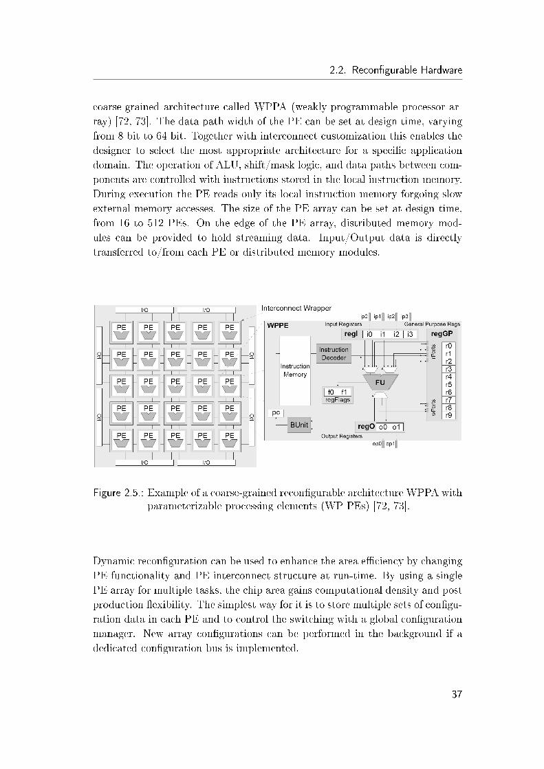
2.2. Recon�gurable Hardware
coarse-grained architecture called WPPA (weakly-programmable processor ar-
ray) [72, 73]. The data path width of the PE can be set at design time, varying
from 8 bit to 64 bit. Together with interconnect customization this enables the
designer to select the most appropriate architecture for a speci�c application
domain. The operation of ALU, shift/mask logic, and data paths between com-
ponents are controlled with instructions stored in the local instruction memory.
During execution the PE reads only its local instruction memory forgoing slow
external memory accesses. The size of the PE array can be set at design time,
from 16 to 512 PEs. On the edge of the PE array, distributed memory mod-
ules can be provided to hold streaming data. Input/Output data is directly
transferred to/from each PE or distributed memory modules.
Figure 2.5.: Example of a coarse-grained recon�gurable architecture WPPA withparameterizable processing elements (WP PEs) [72, 73].
Dynamic recon�guration can be used to enhance the area e�ciency by changing
PE functionality and PE interconnect structure at run-time. By using a single
PE array for multiple tasks, the chip area gains computational density and post
production �exibility. The simplest way for it is to store multiple sets of con�gu-
ration data in each PE and to control the switching with a global con�guration
manager. New array con�gurations can be performed in the background if a
dedicated con�guration bus is implemented.
37

2. Background
2.2.3. Con�gurable Processors
In general, recon�gurable architectures target the acceleration of software. De-
pending on the application, the recon�gurable hardware can be loosely coupled
to a microprocessor via the processor bus or shared memory. This approach
allows to extend a standard computer workstation by attaching an accelerator
card to the Motherboard. The downside of this approach is limited bandwidth
and high communication latency between the host processor and the recon�g-
urable device which forces the accelerator to operate with relative autonomy. In
most cases, compute-intensive data is o�-loaded to the accelerator card and the
results are collected after processing, without intensive communication during
the processing phase. Thus, only compute intensive applications can bene�t
from acceleration. Examples of this loose system coupling include Splash2 [74],
Celoxica RCHTX [75], ClearSpeed [75], and other PCI or PCIe based recon-
�gurable accelerator boards. Other examples are also the Cray XD1 and SGI
RC100 accelerator cards for high performance clusters. They both contain two
large coprocessor FPGAs with access to local high speed memory and custom
communication links which can be used transparently by the software applica-
tions.
In more e�ective schemes for closely-coupled systems, the recon�gurable hard-
ware can be implemented as a coprocessor connected directly or through a
dedicated memory bu�er to the processor. GARP [76], REMARC [77], and
MorphoSys [78] are examples of such architectures.
The integration of a recon�gurable fabric (also called recon�gurable functional
unit) into to the data path of a processor or embedding a microprocessor directly
into an FPGA generates a very tightly coupled system. In the �rst case, the
recon�gurable hardware becomes a integral part of the processor architecture.
The recon�gurable functional unit can be con�gured to compute application
speci�c custom instructions. These instruction can be used like any other pro-
cessor instructions. Through run-time con�guration of the recon�gurable unit
new custom instructions can be created on-the-�y. Examples of these architec-
tures are Stretch S5000 [79], OneChip [80], DISC [81], Chimera [82] and MOLEN
[83].
In the second case, the microprocessor itself is embedded inside the recon�g-
urable hardware. For example, the IBM PowerPC 405 hardcore processor is
physically embedded inside Virtex-II/Pro FPGAs [84]. Another method is to
38

2.3. Partial Recon�guration
generate custom softcore microprocessor for the FPGA which can be customized
to application speci�c needs but occupy valuable logic resources. This is per-
formed with optimized and FPGA speci�c IP-core generators which allow a high
degree of customization. Examples of such softcore microprocessors are Xilinx
MicroBlaze [85], Altera Nios-II [86], and ARM7 processor core [87] for Actel
FPGAs.
2.2.4. Related Computing Platforms
The potential to accelerate supercomputing applications motivated several projects
to explore recon�gurable computing systems. Similar to existing supercomput-
ers, a large number of FPGAs were embedded in dedicated network topologies.
Two examples from the early 1990s are the Splash-II [74] and the Programmable
Active Memory (PAM) [88]. Splash contained 32 and PAM 25 FPGAs. Both
systems proved their impressive performance by outperforming standard super-
computers in several application areas [89].
The Berkeley Emulation Engine [90] is a new member of the high performance
computing arena. The current BBE2 [91, 92] FPGA based platform is designed
to be modular and scalable in order to accelerate a wide range of application
domains such as, real-time signal processing, scienti�c computing, large scale
simulation and emulation. The platform is based on the BEE Motherboard
containing �ve large FPGAs with high speed memory and communication in-
terfaces. Depending on the application requirements a network of BEE Mother-
boards and storage modules is combined to create the recon�gurable computing
system. One example application is the Research Accelerator for Multiple Pro-
cessors Project (RAMP) [93, 94] which emulates a thousand core multiprocessor
system where each FPGA hosts several softcore processors.
2.3. Partial Recon�guration
FPGAs load their con�guration from external memory during start-up or can
be made to do so by asserting a chip reset signal. This means that the FPGA
must be re-programmed entirely and its current internal state is lost. In order
to bene�t from concurrent hardware tasks which can be loaded independently
39

2. Background
during run-time into the FPGA, partial recon�guration and read-back of the
internal hardware task state must be supported [25, 95, 21]. However, loading
tasks into the devices is a sequential process and the overhead for each task is
typically proportional to its con�guration data size.
Whenever possible, a reset of the FPGA should be avoided, because a complete
new con�guration has to be written to the FPGA whereby all internal states
are lost. Partial recon�guration, also known as partial dynamic or run-time
recon�guration, allows partial changes of the FPGA logic without a�ecting the
state of other logic blocks. This means that parts of the FPGA una�ected
by the partial recon�guration process continue to work without any interrupt.
Changes to a small block of logic will be always much faster than recon�guration
of the entire FPGA as the recon�guration overhead is proportional to the chip
area occupied by the logic block. The more con�guration overhead there is, the
more likely is that the system performance will be below that of �xed-hardware
version when partial recon�guration is performed too frequently.
A hardware task is functional hardware component/module that contains its
own con�guration and run-time dependent state information. Hardware module
relocation allows to load and execute a hardware task in any free recon�gurable
region. Hardware modules should be developed in a position-independent way
to be relocatable. However, the con�guration data, sometimes referred to as
bitstream or bit�le, references absolute CLB positions inside the FPGA. This
requires an extra translation step to change the position information inside the
bit�le to the desired recon�guration region. Otherwise, each partial module has
to be synthesized in a separate process for each possible recon�guration region.
To actually carry out a dynamic placement of a hardware module during run-
time, a few assumptions are required. First, it is desirable to add constraints on
the size and shape of the relocatable hardware module. These constraints limit
the number of possible choices within the FPGA and make run-time placement
algorithms more e�cient and e�ective. Second, inter-module and o�-chip com-
munication require �xed communication access points that must be known at
design time of a relocatable hardware task. Hence, every hardware task should
adhere to a standard communication interface. This paves the way for greater
hardware task re-use and is especially important if a hardware task library has
to be maintained.
As most hardware tasks are comparable to functional logic blocks, it is safe
to assume that many existing hardware designs can be split and migrated to
40
2.4. Technical Advantages and Limitations
relocatable hardware tasks. One goal to accomplish this migration in a time
e�ective manner is to build a thin wrapper around the existing logic block with-
out any modi�cations to its original behavior. This task wrapper itself is part
of a hardware task framework which is always present within the recon�gurable
device. The framework itself provides inter-task communication support, ac-
cess to o�-chip peripherals and external memory devices through a standard
interface.
Due to the dynamic nature of recon�gurable computing, it is helpful to have
software components manage various con�guration processes at run-time. These
task can be divided into:
• Deciding which hardware objects to execute, where on the device and
when.
• Swapping of hardware tasks into and out of the recon�gurable logic.
• Switching communication paths between hardware tasks or between hard-
ware tasks and peripheral I/O devices.
This embedded software is analogous to an operating system that manages exe-
cution of multiple software threads. Like threads, hardware tasks may have pri-
orities, deadlines, dependencies and communication/memory constraints. The
goal of the run-time environment is to organize this information and make de-
cisions based upon it. As there are decisions to be made while the system
is running, algorithms have to be developed for on-line scheduling and plac-
ing of hardware tasks. The on-line scheduler is responsible for deciding which
hardware tasks are currently running. However, it is not possible to run tasks
without the placer which manages the 2D free space hardware area within the
recon�gurable device. Moreover, the placer is also responsible for keeping track
of all used communication channels. In order meet all hardware task constraints
communication aware placement has to be combined with the scheduling pro-
cess, as for example it makes no sense to schedule a task for execution when its
memory or communication constraints cannot be met by the placer.
2.4. Technical Advantages and Limitations
Recon�gurable computing has the advantage of greater functional density through
the use of a more simple hardware device. Needed logic blocks can be loaded on
41

2. Background
demand into the recon�gurable device. The high device cost can be reduced to
the low cost of a smaller device and an additional memory required to store the
logic design. Because many new systems have a network connection, this cost
of extra con�guration memory can be cut by implementing on demand update
strategies directly into the operating system of the recon�gurable device.
There are several advantages of recon�gurable computing over general purpose
processors on one hand, and ASICs on the other hand:
• Acceleration of various compute-intensive applications and very high speed
implementations of sequential tasks.
• Easy support for bug �xes and upgrades in the �eld with no down time.
Moreover, recon�gurable devices enable aggressive time-to-market strate-
gies with only core features being implemented on roll out. Missing fea-
tures can be delivered later on via an upgrade. Moreover, this extends the
life cycle of the system, thus reducing costs for the owner.
• Hardware multitasking enables multiple applications to run concurrently
on the same device. This enables true recon�gurable computing with mul-
tiple optimized applications running concurrently on one recon�gurable
device. As parts of the application can be developed independently these
systems can have shorter design and implementation cycles.
• Hardware sharing between hardware tasks is realized because running
tasks can be replaced. Bene�ts are reduced device size, reduced power
consumption and overall lower costs.
• Shorter recon�guration times through partial recon�guration enable fre-
quent recon�guration changes if required by the application. This enables
self-adaptive systems which deliver consistent performance in changing
environments.
However, there are three main limitations which need to attract more attention
in order to move recon�gurable computing towards mainstream adoption.
Compilers and back-end tools for recon�gurable computing are still under devel-
opment. Not only are e�cient high level compilers supporting partial recon�gu-
ration missing but also the low level back-end tools coming from corresponding
42

2.4. Technical Advantages and Limitations
chip vendors must be improved for a productive design environment [19]. Com-
mercial support for partial recon�guration must also be available together with
a well de�ned design �ow.
Debugging support for partial recon�guration is currently not available as a
debugging methodology including supporting tools is not available. Clock dis-
tribution and communication channels in recon�gurable systems are another
problem source.
Finally, the inability to verify run-time recon�gurable systems is an obstacle
for medical, aeronautical and mission critical control systems. The only viable
option is to emulate the run-time behavior. This can be done by implementing
all partial recon�gurable tasks at the same time on a much larger device and
to select the correct module through additional multiplexers. However, the
recon�guration is only emulated and the recon�guration process itself is not
performed.
43

2. Background
44

3. The Erlangen Slot Machine
3.1. Introduction
Partial recon�guration requires run-time loadable modules that are pre-compiled
and their bitstreams are stored in an external memory device, which will then
be used to recon�gure a dedicated region on the FPGA. Several models and
algorithms for on-line placement have been developed in the past, see e.g.,
[96, 97, 98, 3]. However, these algorithms are limited by two main factors.
First of all, the model assumptions are often not realistic enough for implemen-
tation on real hardware or require a tedious development process. Second, the
development process of recon�gurable modules is subject to many restrictions
that make a systematic development process for partial recon�guration di�cult.
Until now, no FPGA-based platform on the market provides a solution to the
problems of design automation for dynamically recon�gurable hardware modules
and their e�cient and �exible relocation. The purpose of the Erlangen Slot
Machine (ESM) [4, 99, 100, 101, 45, 40, 42] is to overcome many of the
de�ciencies of existing FPGA-based recon�gurable computers by providing:
• A new �exible FPGA-based recon�gurable platform that supports relo-
catable hardware modules arranged in so-called slots.
• Tool support for the development of run-time recon�gurable computa-
tion and communication schemes using new inter-module communication
paradigms.
45

3. The Erlangen Slot Machine
• A powerful recon�guration manager which enables various pre-processing
stages for fast bitstream manipulation. We call the pre-processing stages
plug-ins. For example, a relocation plug-in can be selectively activated
before a bitstream is uploaded to the FPGA.
Recon�guration times in the range of seconds [102] are not su�cient for ap-
plications that require a fast reaction to external events. Our hardware recon-
�guration manager is the foundation for recon�guration times in the range of
milliseconds. For example, these fast recon�guration times will allow a seamless
switching of video �lters in a video pipeline processing architecture.
The main goal of the Erlangen Slot Machine's architecture [99, 100, 103, 2] is
to accelerate application development as well as research in the area of partially
recon�gurable hardware. The Erlangen Slot Machine owes its name to this
arrangement of recon�gurable slots which can be changed independently. This
modular organization of the device simpli�es the relocation, primary condition
for a viable partially recon�gurable computing system. Each module moved
from one slot to another will come across equal resources.
The advantage of the ESM platform is its one dimensional (1D) slot-based
architecture with support for varying slot widths. Slots are prede�ned recon�g-
urable regions in which hardware tasks can be exchanged during run-time. The
slot architecture on the ESM enables the execution of independent as well as
communicating hardware tasks by delivering peripheral data through a separate
crossbar switch to each slot. This is shown in Figure 3.1.
We decided to design an o�-chip crossbar in order to leave as many resources
free on the FPGA for partially recon�gurable modules. The ESM architecture is
based on the �exible decoupling of the FPGA I/O-pins from a direct connection
to an interface chip. This �exibility allows independent placement of application
modules in any available slot at run-time. Thereby, run-time placement is not
constraint by physical I/O-pin locations, as the I/O-pin routing is performed
automatically in the crossbar; thus, the I/O pin dilemma is solved in hardware.
The ESM platform, as shown in Figure 3.1, is centered around a large FPGA
serving as the main recon�gurable engine and a second FPGA realizing the
crossbar switch for peripheral I/O access. These two FPGAs are placed on two
physical boards, called Babyboard and Motherboard. The main recon�g-
urable device is a Xilinx Virtex-II 6000 FPGA and located on the Babyboard.
46

3.1. Introduction
Crossbar
Mai
n FP
GA
ESM Babyboard
PowerPC
ReconfigurationManager
Flash …
ESM Motherboard
SDRAM
SRAM SRAM SRAM SRAM
S3 SNS2S1
Peripherals
Figure 3.1.: ESM architecture overview with main FPGA, crossbar and an ex-ternal PowerPC microprocessor for system control functions. Thearchitecture of the Babyboard is further re�ned in Figure 3.7. TheMotherboard is shown in Figure 3.12.
The crossbar is implemented by a Xilinx Spartan-IIE 600 FPGA and located
together with all peripheral I/Os on the Motherboard. Figure 3.1 shows the
slot-based architecture of the ESM consisting of the Virtex-II 6000 FPGA, local
SRAM, con�guration memory and a recon�guration manager FPGA.
The number of recon�gurable slots depends on the number of I/O pins needed
for SRAM access. If SRAM access is not required then the slot width depends
only on the number of I/Os connected to the crossbar interface. All I/O blocks
of the main FPGA are located at the edges of the device, as shown in Figure
2.2. The top pins in the north of the FPGA connect to local SRAM banks.
These SRAM banks thus solve the problem of restricted intra-module memory,
in the case of video applications, for example. The bottom pins in the south
connect to the crossbar switch. Therefore, a module can be placed in any free
slot and have its own peripheral I/O-links together with dedicated local external
47
3. The Erlangen Slot Machine
memory. The slot width is only prede�ned if hardware modules require access
to the external SRAM. This is due to the �xed number of signals needed to
access and to control one SRAM device.
3.2. Communication Models
One of the central limiting factors for the wide use of partial dynamic recon�g-
uration yet not addressed is the problem of inter-module communication. Each
module that is placed on one or more slots on the device must be able to com-
municate with other modules. For the ESM, we investigated and provide four
main paradigms for communication among di�erent modules, as shown in Figure
3.2. The �rst one, is a direct communication using bus-macros [104, 105, 106]
between adjacently placed modules. Secondly, shared memory communication
using SRAMs or BlockRAMs is possible. However, only adjacent modules can
use these two communication modes. For modules placed in non-adjacent slots,
we provide a dynamic signal switching communication architecture called re-
con�gurable multiple bus (RMB) [107, 46]. In [108] we presented an ILP model
for minimizing the communication cost for RMB slot modules. Finally, the
communication between two di�erent modules can also be realized through the
external crossbar.
Communication between Adjacent Modules On the ESM, bus-macros are
used to realize a direct communication between adjacently placed modules, pro-
viding �xed communication channels that help to keep the signal integrity upon
recon�guration. Bus-macros provide a means of locking the routing between
partial recon�gurable modules (PRMs) and the static base design, making the
PRMs pin compatible with the base design. As a result, all connections be-
tween the PRMs and the base design must pass through a bus-macro, with
the exception of the clock signal (global signals, GND and VCC, are handled
automatically by the Xilinx design �ow tools in a way that is transparent to
the user). As stated in Section 2.2.1 on page 35, eight signals can be passed
through each standard Xilinx bus-macro [21]. Hence, the number of bus-macros
needed to connect a set of n signals between two PRMs is dn/8e. The use of
custom build bus-macros would allow to de�ne the data width per bus-macro
arbitrarily, but requires extensive overhead to design and manually route the
hard macro.
48

3.2. Communication Models
FPGA
SRAM SRAM SRAM
S3S2S1
FPGA
SRAM SRAM SRAM
S3S2S1
FPGA
S3S2S1
Crossbar
FPGA
S3S2S1
Crossbar
FPGA
S3S2S1
FPGA
S3S2 S1S1
FPGA
S3S2S1
FPGA
S3S2S1
a) b)
d)c)
Figure 3.2.: Inter-module communication possibilities on the ESM: a) bus-macro, b) shared memory, c) recon�gurable multiple bus (RMB),d) external crossbar. Hardware modules can also with software run-ning on the PowerPC microprocessor via the crossbar.
Communication via Shared Memory Communication between two neigh-
boring modules can be done in two di�erent ways using shared memory: First,
dual-ported BlockRAMs can be used for implementing communication among
two neighbor modules working in two di�erent clock domains. The sender writes
on one side, while the receiver reads the data on the other side. The second
possibility uses external RAM. This is particular useful in applications in which
each module must process a large amount of data and then sends the processed
data to the next module, as it is the case in video streaming.
On the ESM, each SRAM bank can be accessed by the module placed below as
well as those neighbors placed right and left. A controller is used to manage the
49

3. The Erlangen Slot Machine
SRAM access. Depending on the application, the user may set the priority of
accessing the SRAM for the three modules.
Communication via RMB In its basic de�nition, the Recon�gurable Multi-
ple Bus (RMB) architecture [109, 110, 46, 47] consists of a set of processing
elements or modules, each possessing an access to a set of switched bus connec-
tions to other processing elements. The switches are controlled by connection
requests between individual modules.
The RMB is a one-dimensional arrangement of switches between N slots (see
Figure 3.3). In our FPGA implementation, the horizontal arrangement of par-
allel switched bus line segments allows for the communication among modules
placed in the individual slots. The request for a new connection is done in a
wormhole fashion, where the sender (a module in slot Sk) sends a request for
communication to its neighbor (slot Sk+1) in the direction of the receiver. Slot
Sk+1 sends the request to slot Sk+2, etc., until the receiver receives the request
and returns an acknowledgment. The acknowledgment is then sent back in the
same way to the sender.
SRAM
Reconfigurable Multiple Bus (RMB)
FPGA
S1
CP1
SRAM
S2
CP2
SRAM
S3
CP3
SRAM
S4
CP4
SRAM
S5
CP5
SRAM
S6
CP6
Figure 3.3.: ESM slot architecture with six macro-slots (S1, S2, ... S6). In orderto allow access to the RMB crosspoints (CP) and SRAM banks, onemacro slot consists of three micro-slots. Physically, one micro-slotoccupies exactly four CLB columns.
50

3.2. Communication Models
Each module that receives an acknowledgment sets its switch to connect two
line segments. Upon receiving the acknowledgment, the sender can start the
communication (circuit routing). The wired and latency-free connection is then
active until an explicit release signal is issued by the sender module. The con-
cept of an RMB was �rst presented in [110] and extended later in [109] with
a compaction mechanism for quickly �nding a free segment. However, it has
never been implemented in real hardware.
In our implementation [111] of an RMB architecture on Xilinx Virtex FPGAs,
we separated the RMB switches from the modules. In this way, we provide
a uniform interface to designers for connecting modules to the multiple line
switches. The implementation of the RMB structure on an FPGA Virtex II
6000 with four processors and four parallel 16 bit lines reveals an area overhead
of 4% with a frequency of 120 MHz for the RMB controller [107]. Here, we
have summarized area and data speed numbers in terms of a) di�erent numbers
of modules, b) di�erent numbers of parallel bus segments, and c) bit widths of
each bus segment. Special bus-macros are used at the boundary of modules and
controllers to ensure a correct operation upon recon�guration.
We were able to show that a module recon�guration can take place column-wise
at the same time that other modules are communicating on the chip without any
signal interference. This is possible by storing the states of the RMB switches in
regions of BlockRAM that are physically una�ected by partial recon�guration.
Communication via the Crossbar Another possibility of establishing a com-
munication among modules is to use the crossbar. Because all the modules are
connected to the crossbar via the pins at the south of the FPGA, the commu-
nication among two modules can be set in the crossbar as well.
Communication Costs The ESM platform supports the four mentioned com-
munication schemes for inter-module communication. Each approach has its
own properties, such as maximum bandwidth, signal delay and setup latency.
The RMB is the only scheme that has a varying setup latency that is the product
of the number of RMB elements to destination and the setup time of four clock
cycles. Using bus-macros for communication is the preferred choice, but it only
works for adjacent modules. The maximum bandwidth in all communication
51

3. The Erlangen Slot Machine
schemes is a factor of clock speed and data bandwidth. We assume for the ESM
a global clock speed of 50 MHz. All properties are listed in Table 3.1.
Communication scheme Data Bandwidth Latency Setup
Bus-macro 19.2 Gbit/s 2 ns noneRMB 6.4 Gbit/s 3 ns * CP 4 cycles * CPCrossbar 1.8 Gbit/s 15 ns 18 cyclesSRAM 0.4 Gbit/s 20 ns 2 cycles
Table 3.1.: Theoretical data bandwidth and signal latency for the four supportedcommunication schemes. Variable CP denotes the number of RMBCross Points that are traversed.
3.3. Implemented Architecture
The Erlangen Slot Machine was designed as a two-board solution, consisting
of Babyboard and Motherboard. The separation of ESM into a Babyboard
and a Motherboard was made to simplify the adoption of the ESM platform to
other application domains such as automotive. In order to do so, only a new
Motherboard can be designed to have di�erent peripherals such as CAN, LIN,
FlexRay controllers, and A/D and D/A converters. The Babyboard design can
remain unchanged and can be used with di�erent application domain speci�c
Motherboards.
The schematic of the whole ESM platform is illustrated in Figure 3.4 and its
two-board implementation is shown in Figure 3.5. The recon�guration manager
(RCM) is implemented in a Spartan-IIE 400 FPGA which is connected to a 64
MByte �ash device on the Babyboard. Six SRAM banks, two MByte each, are
attached to the north side of the FPGA. They provide memory space to six
macro-slots (denoted as S1 to S6 in Figure 3.3) for temporal data storage. The
SRAMs can also be used for shared memory communication between neighbor
modules, e.g., for streaming applications. They are connected to the FPGA in
such a way that the recon�guration of a given module will not a�ect the access
to other modules. Debugging capabilities are o�ered through general purpose
I/O provided at regular distances between the micro-slots.
52

3.3. Implemented Architecture
Flash
Main FPGAMain FPGA
CPLD RCMFPGARCMFPGA
EPP
SRAM
VideoOutFPGA
VideoOutFPGA
CrossbarFPGA
CrossbarFPGA
SDRAM
SDRAM
SDR
AM
PowerPC
DVI
VGA
CVBS
S-Video
Ethernet USB Serial
Audio
SRA
M
SRA
M
SRAM
SRA
M
SRA
M
Babyb oardM
othe rboa rd
Debug I/O
SDRAM
Flash
S-Video
Figure 3.4.: Schematic diagram of the ESM shows the implemented two-boardsolution with an FPGA Babyboard and a supporting Motherboard.
A JTAG port provides debug capabilities for the main FPGA, the Spartan-
II FPGA and a CPLD. All technical data sheets as well as software, primer
applications, and additional information are available at the following website:
http://www12.informatik.uni-erlangen.de/research/esm. An actual picture of
53

3. The Erlangen Slot Machine
the two ESM boards is shown in Figure 3.5.
Figure 3.5.: ESM implementation of the FPGA Babyboard and the supportingMotherboard. On top of the Motherboard sits the Babyboard withthe Virtex-II 6000 FPGA. Additional technical data and examplesare available at http://www.r-space.de.
Slot Arrangement The main FPGA of the ESM is organized into twenty-two
so-called micro-slots with twelve I/O-pins each, as the Virtex-II FPGA can only
be recon�gured column-wise. This is shown in Figure 3.6. Because the left and
right slots of the FPGA are connected to dedicated I/Os, one micro slot on
both the left and the right side of the FPGA is excluded for use in partially
recon�gurable designs. As the middle CLB columns are connected to external
clock lines, two micro-slots in the middle of the device are also excluded. Three
micro-slots can be grouped logically into one macro-slot in order to allow access
to the RMB and SRAM banks. An overview is shown in Figure 3.3 and the
resulting micro-slot architecture is shown Figure 3.6. Due to the incorporation
of BlockRAM and multipliers, the Virtex-II FPGA architecture from Xilinx is
divided into columns. Each BlockRAM block occupies a whole column in the
device; the XC2V6000 FPGA has six slots that are spread over the device.
Therefore, only macro-slots one and four contain one BlockRAM column.
Slots A to V denote micro-slots that provide the module and recon�guration
granularity. Three consecutive micro-slots de�ne a macro-slot. Each macro-slot
54
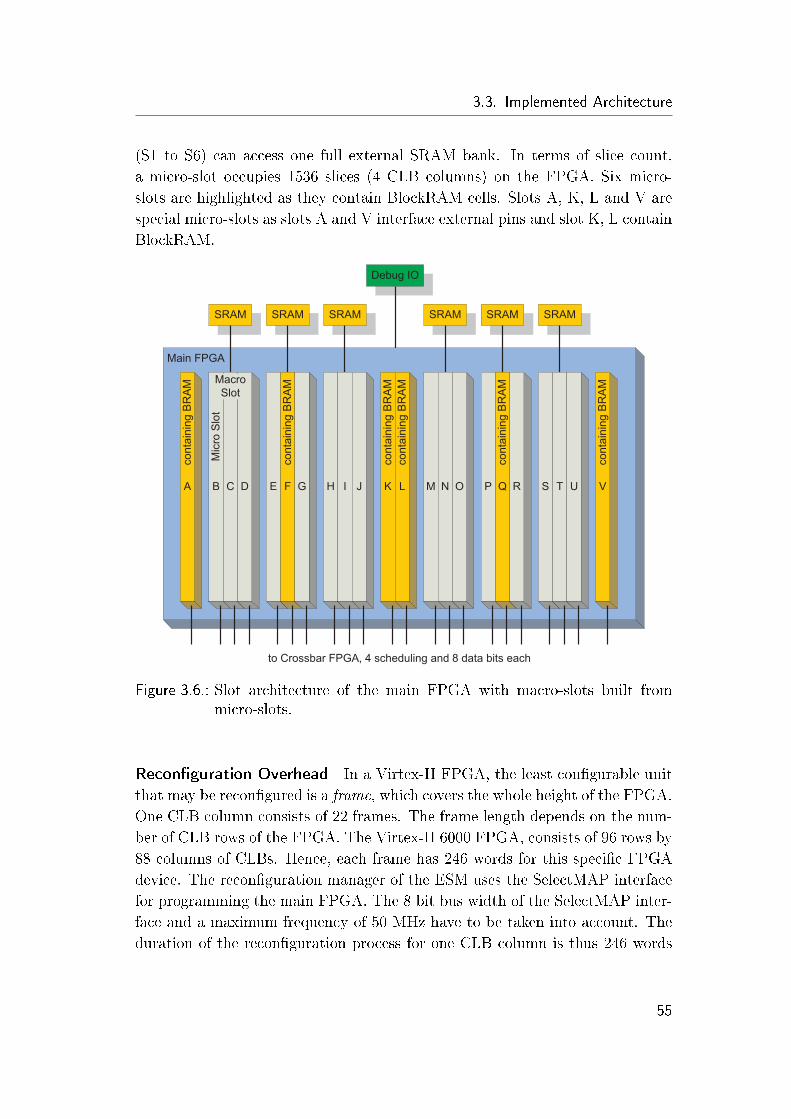
3.3. Implemented Architecture
(S1 to S6) can access one full external SRAM bank. In terms of slice count,
a micro-slot occupies 1536 slices (4 CLB columns) on the FPGA. Six micro-
slots are highlighted as they contain BlockRAM cells. Slots A, K, L and V are
special micro-slots as slots A and V interface external pins and slot K, L contain
BlockRAM.
Figure 3.6.: Slot architecture of the main FPGA with macro-slots built frommicro-slots.
Recon�guration Overhead In a Virtex-II FPGA, the least con�gurable unit
that may be recon�gured is a frame, which covers the whole height of the FPGA.
One CLB column consists of 22 frames. The frame length depends on the num-
ber of CLB rows of the FPGA. The Virtex-II 6000 FPGA, consists of 96 rows by
88 columns of CLBs. Hence, each frame has 246 words for this speci�c FPGA
device. The recon�guration manager of the ESM uses the SelectMAP interface
for programming the main FPGA. The 8 bit bus width of the SelectMAP inter-
face and a maximum frequency of 50 MHz have to be taken into account. The
duration of the recon�guration process for one CLB column is thus 246 words
55

3. The Erlangen Slot Machine
(each 32 bit) ∗ 22 frames ∗ 4 clock cycles ∗ 20 ns = 433µs.
3.4. The Babyboard
The recon�gurable engine of the Erlangen Slot Machine consists of a Xilinx Vir-
tex II-6000 FPGA, several SRAMs, a recon�guration FPGA and �ash memory.
They all are placed on a high density printed circuit board (PCB). This PCB is
called the Babyboard and has four connectors to the Motherboard. Due to the
restriction 1 in the recon�guration process of Virtex-II FPGAs, the architec-
ture has been optimized to solve the major problems of partial recon�gurable
hardware platforms, namely:
Solving the I/O-pin dilemma: Run-time placement of modules on a recon�g-
urable device, in this case the FPGA, is done by downloading a partial bit-
stream that implements the module on the FPGA. This requires a relocation
that places a module in a location di�erent from the one for which it was syn-
thesized. Relocation can be done only if all the resources are available and
structured in the same way in the designated placement area at compile-time.
This includes also the I/O-pins used by the module. For example, a module
compiled for slot 0 might then be allocated to slot 3 at run-time. We solved
the I/O-pin dilemma on the ESM by avoiding �xed connections of peripherals
to the FPGA. As shown in Figure 3.7, all the bottom pins from the FPGA are
connected to an interface controller realizing a crossbar and implemented itself
using a Xilinx Spartan-II FPGA. At run-time, the crossbar connects FPGA
pins to peripherals automatically based on the slot position of a placed module.
This I/O-pin rerouting principle is done without recon�guration of the cross-
bar FPGA. The solution is to implement con�guration registers in the crossbar
which can be read and written at module load time by the PowerPC micro-
processor located on the Motherboard. This makes it possible to establish any
connection from one module to peripherals dynamically.
Solving the memory dilemma: Memory is very important in applications like
video streaming in which a given module must exclusively access a picture at
a time for computation. However, as we mentioned earlier, the capacity of the
available BlockRAMs in FPGAs is limited. External SRAMmemory is therefore
1The recon�guration can be done only in chunks of full columns.
56

3.4. The Babyboard
added to allow storage of large amounts of data by each module. To allow a
module to exclusively access its external memory bank, six SRAM banks are
connected at the north border of the FPGA. In this way, a module will connect
to peripherals from the south, while the north will be used for temporally storing
computation data. According to the physical layout of the six memory banks
which are connected to the top I/O pins, the FPGA device is divided into a
set of elementary slots called micro-slots A to V as shown in Figure 3.6. In
order to use an SRAM bank in the north, a module must have at least a width
of three micro-slots (creating slots S1 to S6).
Flash
Main FPGAMain FPGA
CPLD RCMFPGARCMFPGA
EPP
SRAM
SRA
M
SRA
M
SRAM
SRA
M
SRA
M
Babyb oard
Debug I/O
To crossbar FPGA on the Motherboard
Figure 3.7.: The main components of the Babyboard are the main FPGA for userapplications, a Recon�guration Manager (RCM) FPGA for con�gu-ration management, and a CPLD for the initialization routines afterpower-up.
The basic layout of the Babyboard is depicted in Figure 3.7. Applications
contain tasks that consist each of a module request. They are located on the
main FPGA, a Xilinx Virtex-II 6000 device. This FPGA is connected to six
SRAM memories, two Megabytes each, which can be accessed independently
by di�erent applications. Each of the twenty-two micro-slots has its own debug
57

3. The Erlangen Slot Machine
I/O pin that is externally accessible. These twenty-two Debug I/O signals can
be used for visualization, a dedicated debug interface or as special interface,
i.e. for a CAN bus module. The main FPGA is linked to the Motherboard via
264 bits clustered in so called I/O signals.
The implemented ESM Babyboard is shown in Figure 3.8. It contain the follow-
ing components on a 12-layer PCB: the main FPGA is a Xilinx Virtex-II 6000
(1), the recon�guration manager FPGA is used to control the �ash memory and
recon�guration process of the main FPGA (2), 64 MByte of �ash memory are
used to store full and partial bitstream for the main FPGA (3), a CPLD used to
initialize the �ash memory and the recon�guration manager (RCM) at start-up
(4), six SRAM banks with a size of of 2 MByte each (5), optional SO-DIMM
memory socket for DDR memory, and external debug I/Os for independent
status monitoring of partial recon�gurable modules.
Figure 3.8.: The ESM Babyboard and its components.
The Recon�guration Manager, herein after referred to as RCM, enables the dy-
58

3.4. The Babyboard
namic recon�guration ability of the ESM platform. It programs the main FPGA
via the SelectMAP interface with the bit�les stored in the attached �ash mem-
ory. The RCM is controlled and supplied with bit�les by the PowerPC micro-
processor mounted on the Motherboard. Additionally it provides an Enhanced
Parallel Port (EPP) interface which also allows external control and debugging
of the recon�guration process.
The CPLD runs the initialization routines for the board upon power-up, e.g.
programming a PLL for the required clocks and con�guring the RCM with a
start-up con�guration stored in �ash memory. After completed power-up of the
recon�guration FPGA the CPLD goes itself into an idle state and disconnects
form the �ash memory bus which is then controlled by the RCM.
3.4.1. Main FPGA
The actual workhorse of the ESM is a Xilinx Virtex-II 6000, called main FPGA.
This FPGA has an almost homogeneous CLB area of 96 × 88 CLBs, as shown
in Figure 3.6, and was the only readily available FPGA of its size at the time
of the �rst design of the ESM architecture. With more than 88.000 logic cells,
scores of applications can be implemented in hardware [25].
On the ESM the FPGA's logic area is divided into twenty-two micro-slots to
empower an organized recon�guration and relocation of hardware modules [99,
100]. Each slot spans the same area and has the same amount of I/Os at its
disposal, four control and eight data bits. Additionally, there are six special
micro-slots which contain 24 BlockRAM elements each. The arrangement can
be seen in Figure 3.6. It also depicts the clustering into the already mentioned
macro-slots. This coarse partition is intended for more extensive modules which
need a large amount of memory. For these purposes, six asynchronous SRAMs
are attached at the top of the main FPGA.
The hardware modules on the main FPGA have di�erent options to communi-
cate with other modules. To maximize placement �exibility, the Crossbar can
establish point-to-point connections between any I/O groups.
Bus-macros are the �rst choice for high data rate communication between hard-
ware tasks then. They are instantiated along the module borders and allow ad-
jacent modules to communicate directly with each other. However, this implies
59

3. The Erlangen Slot Machine
preassigned positions according to the design choice made during the compile
time of each hardware module. A solution for this issue is presented in [107, 46],
the Recon�gurable Multiple Bus on Chip. The mentioned use of the SRAMs as
shared memory is technically equal to bus-macro communication except for the
inherent bu�ering and the overhead for each read/write access.
To implement an application on this device the top-level VHDL entity, or ac-
cording Verilog module, should have ports for the I/Os listed in Table 3.2. When
developing modules for partial recon�guration, the Xilinx Early Access Partial
Recon�guration user guide [95, 21] should be followed.
Width Port Description
22x4 bits Scheduling_A-V Scheduling �ags for each Micro Slots
22x8 bits XbarIO_A-V Data I/O for each Micro Slot
6x20 bits sram_a SRAM address, shared with two chips
6x8 bits sram_d SRAM data, shared with two chips
6x2 bits sram_oe_neg SRAM output enable, for each chip
6x2 bits sram_we_neg SRAM write enable, for each chip
6x1 bit sram_ce_neg SRAM chip enable, shared with two chips
22 bits debug_io For LEDs or special adaptors like a CANcontroller
6 clocks clk PLL clock signals
Table 3.2.: Interface of the main FPGA
3.4.2. The Recon�guration Manager
The ESM platform requires an operating system for the initialization of exe-
cutable application modules and their run-time supervision. The main tasks of
such an operating system are:
• scheduling of application modules,
• management of free slots including slot segmentation and partitioning,
60

3.4. The Babyboard
• loading, unloading and relocation of application modules into slots,
• con�guration of peripheral devices,
• con�guration of the crossbar, and
• bitstream management.
In our view, the most-time critical operations must be executed in hardware
in order to keep the recon�guration time at a minimum. We consider loading,
unloading and relocation of modules to be the most time critical tasks which
will be therefore implemented in a dedicated hardware Recon�guration Manager
(RCM) [43, 42]. All other system tasks can implemented in software and exe-
cuted on the PowerPC embedded microprocessor that is mounted on the ESM
Motherboard. These two parts of the operating system are linked via a simple
communication bus as shown in Figure 3.1. This hardware/software interface
between the RCM and the PowerPC is realized through a set of elementary
recon�guration instructions passed from the PowerPC to the recon�guration
manager on the Babyboard using memory mapped I/O communication. The
bene�t of this communication method is a simple read/write access to a range
of memory addresses which are physically located inside the Crossbar FPGA.
In its basic form, the recon�guration manager must implement the following
minimal set of elementary instructions:
• LOAD: load bitstreams to their pre-compiled position,
• UNLOAD: unload bitstreams to deactivate a running module,
• RELOCATE_AND_LOAD: relocate bitstreams to a di�erent slot posi-
tion before loading.
Recon�guration Architecture Apart from the main FPGA, the Babyboard
also contains the con�guration circuitry. This consists of a CPLD, a con�gura-
tion FPGA implementing the recon�guration management and a �ash memory
device, as shown in Figure 3.7. A Xilinx Spartan-IIE 400 device implements
the Recon�guration Manager. It comprehends a Xilinx MicroBlaze processor to
control various I/O modules, e.g. the �ash memory or the SelectMAP interface
of the main FPGA.
61

3. The Erlangen Slot Machine
• The CPLD is used to download the Spartan-IIE FPGA con�guration from
the Flash upon power-up. It also contains board initialization routines for
the on-board PLL and the Flash.
• The recon�guration management is implemented on the Spartan-II FPGA.
It is also responsible for the con�guration of the main FPGA during power-
up and run-time. This device also contains a circuit to perform module
relocation while loading a new partial module bitstream.
• The Flash provides a capacity of 64 MByte, thus enabling the storage of
up to 30 full con�gurations or of a few hundred partial module bitstreams
typically.
During normal operation, bitstream data is loaded from the �ash memory into
the main FPGA through the SelectMAP interface (see Figure 3.7). However,
bitstreams must be downloaded from a host PC and then stored in the �ash
memory device. Here, two methods are supported. The �rst method uses a par-
allel port interface implemented inside the recon�guration manager to download
the con�guration data from a host PC to the �ash memory. The second method
uses the Ethernet port of the PowerPC microprocessor to download bitstreams
from a remote host. In order to support these and also many other recon-
�guration scenarios, we developed an extensible, plug-in based recon�guration
manager architecture that will be described next.
Flexible Plug-in Architecture Our �rst implementation had a block oriented
recon�guration manager and consisted of a simple state machine which con-
trolled all interfaces and operated on byte blocks. These data blocks, 512 bytes
each, correspond to the page size of the �ash memory device. For each primi-
tive operation on a data block, an instruction had to be processed. When one
data block was written from �ash into the Virtex-II SelectMAP interface, two
instructions had to be processed. First, the data block was read in 512 cycles
from the �ash device and written to an internal scratch pad. Then, the second
instruction was read and the data block from the scratch pad was written to
the SelectMAP interface. As all instructions were executed sequentially, the
maximum upload speed of a bitstream to the FPGA was slowed down by factor
two, due to the exclusive access to the scratch pad.
However, the main problem with this architecture arose when extensions were
to be added to the recon�guration manager. If for example, an error correcting
62

3.4. The Babyboard
code (ECC) plug-in and a decompression plug-in are used additionally, then the
throughput of the recon�guration manager will be decreased by a factor of six.
This is due four additional instructions that are needed to read and write the
internal the scratch pad. This initial scenario is illustrated in Figure 3.9 b). An
additional maintenance issue is the global �nite state machine itself. Its code
base had to be changed every time a new plug-in was added or removed.
StateMachine,
Scratch Pad
Virtex2
RelocatorECC
Flasha)
StateMachine,
Scratch Pad
Virtex2
Flashb)
Figure 3.9.: Simple recon�guration manager architecture.
Clearly, this �rst block oriented architecture is not suitable for a high perfor-
mance solution, since the throughput decreases with every new attached plug-in.
The main bottleneck is not the �ash interface but the scratch pad-oriented data
�ow combined with the sequential execution of each instruction.
Based on these consolidated �ndings, we propose a novel architecture for the re-
con�guration manager which can upload bitstreams into the FPGA at the speed
of the �ash interface. The central scratch pad was eliminated and replaced by a
pipelined data �ow architecture. Moreover, a) the �nite state machine was re-
placed by a MicroBlaze microcontroller [85], and b) a data crossbar is employed
between plug-ins to enable customizable communication paths. This new archi-
tecture is depicted in Figure 3.10. The crossbar plug-in shown in this �gure is a
communication interface between the RCM software running on the MicroBlaze
controller and the ESM Motherboard with is PowerPC microprocessor shown
in Figure 3.1. The RCM software controller receives its instructions and new
bitstreams form the PowerPC, through the crossbar communication plug-in.
All plug-in modules are connected to two communication interfaces: The control
bus connects plug-ins to the MicroBlaze for initialization and control. The data
crossbar connects to the data input and output ports of each plug-in. The
setup of the data crossbar also controlled by the MicroBlaze software and can
be dynamically changed during run-time.
63

3. The Erlangen Slot Machine
In order to upload a hardware module from �ash to the FPGA, the following
sequence of steps has to be performed:
1. Command is sent to the MicroBlaze to upload a bitstream to the FPGA
without the use of any other plug-ins.
2. Program running on the MicroBlaze connects the output of the �ash plug-
in to the Virtex-II plug-in input through a write into the con�guration
register of the data crossbar.
3. Next, this program initializes the �ash plug-in with the start address and
length of the bitstream.
4. Then, the program enables the SelectMAP interface in the Virtex-II plug-
in.
5. Finally, the �ash plug-in is enabled and starts to read the bitstream.
6. The �ash plug-in sends the bitstream to the Virtex-II plug-in byte by byte
as long as its ready signal is true (if not, the �ash plug-in has to wait).
7. While the �ash and the Virtex-II plug-in are running in parallel, the Mi-
croBlaze checks periodically if any of the plug-ins has �nished its opera-
tion.
8. Only if after �nishing one command, the MicroBlaze can execute a new
command, and, for example, reinitializes the plug-ins and the data cross-
bar.
If one load command has been executed and another load follows, then the pro-
cedure starts from second step, because the data crossbar has already been set.
The addition of plug-ins to the recon�guration manager is simple. Any new mod-
ule must have a �xed control bus interface and a �xed data crossbar interface.
With these standard interfaces, the plug-in can be directly controlled through
the MicroBlaze assembly program. The data crossbar uses a parametrized HDL
description which can be con�gured at design-time to the number of actually
instantiated plug-ins.
Workload Scenarios Depending on the operating system requirements, dif-
ferent operations need to be performed on each bitstream. Before the bitstream
64

3.4. The Babyboard
MicroBlaze
ECC
Virtex2
Relocator
Crossbar
Flash
Control Bus Data Crossbar
External I/O
External I/O
External I/O
Figure 3.10.: Architecture of the ESM recon�guration manager with plug-inssuch as Flash, ECC, module relocator and other possible plug-ins.
is uploaded to the FPGA, it can pass through any number of additional plug-
ins. The order in which a bitstream passes the plug-ins is con�gurable at run-
time through the setup of the data crossbar switch. This allows a �exible pre-
processing of the bitstream prior to being loaded. Only the number of available
plug-ins in the recon�guration manager has to be determined at design-time.
Based on the introduced recon�guration manager architecture from Figure 3.10,
several �ows are possible. Some of these are depicted in Figure 3.11. In the �rst
scenario, only a basic upload of a bitstream is performed. Therefore, the data
�ows from the �ash plug-in output directly through the data crossbar to the
Virtex-II plug-in input. If an error-correction is needed, then the �ash output
data can be sent to the ECC plug-in before going to the Virtex-II plug-in. This
case is shown in Figure 3.11 b). In the third scenario, the bitstream is read
from the �ash, error-corrected and relocated before being sent to the Virtex-II
plug-in for upload (see Figure 3.11 c)). Here, the crossbar is con�gured by the
microprocessor in such a way that the output of each plug-in is connected to
the input of its neighboring plug-in. The fourth scenario depicted in Figure
3.11 d) shows how the bitstream data is delivered by the PowerPC through
the Motherboard crossbar. The bitstream is subsequently error-corrected and
relocated prior to its upload.
The plug-ins that are currently implemented for the recon�guration manager
65

3. The Erlangen Slot Machine
MicroBlaze
ECC
Virtex2
Relocator
Crossbar
Flash
Control Bus Data Crossbar
a)
MicroBlaze
ECC
Virtex2
Relocator
Crossbar
Flash
Control Bus Data Crossbar
b)
MicroBlaze
ECC
Virtex2
Relocator
Crossbar
Flash
Control Bus Data Crossbar
c)
MicroBlaze
ECC
Virtex2
Relocator
Crossbar
Flash
Control Bus Data Crossbar
d)
Figure 3.11.: Four di�erent workload scenarios for the recon�guration manager.
are: ECC plug-in, decompression plug-in and a relocator plug-in which can
translate a bitstream on the �y to any slot location on the FPGA by directly
manipulating the address o�sets in the bitstream at load-time.
The recon�guration manager was implemented and consists of the MicroBlaze
microcontroller, parallel port interface plug-in, �ash memory interface plug-
in, Virtex-II SelectMAP plug-in, an OPB (on-chip peripheral bus) interface
implementing the control bus and the data crossbar. The control bus is a 32 bit
OPB bus, while the data crossbar is an 8 bit full duplex crossbar.
66

3.5. The Motherboard
3.5. The Motherboard
The Motherboard of the ESM platform, as illustrated in Figure 3.12, provides
programmable links from the FPGA to all multimedia and communication pe-
ripherals, such as USB, Ethernet, Video Input and Output, and Audio-I/Os. It
also links the PowerPC with the RCM for recon�guration actions. The PowerPC
is them main controller of the ESM system and running Linux. Its memory bus
is connected directly to the crossbar for memory-mapped communication with
the recon�guration manager on the Babyboard.
Video-OutFPGA
Video-OutFPGA
CrossbarFPGA
CrossbarFPGA
SDRAM
SDRAM
SDR
AM
PowerPC
DVI
VGA
CVBS
S-Video
Ethernet USB Serial
Audio
Mothe rboa rd
SDRAM
Flash
To RCM FPGA To main FPGA
S-Video
Figure 3.12.: The main component of the Motherboard is the Crossbar FPGAwhich connects all peripherals, PowerPC, and Video-Out FPGAwith the main FPGA on the Babyboard.
The physical connections are established at run-time through a programmable
crossbar implemented on a Spartan-IIE FPGA device on the Motherboard.
Video capture and rendering interfaces as well as high speed communication
links are also located on the Motherboard. The Babyboard is mounted through
four connectors on top of the Motherboard. An embedded Linux [112] has been
67

3. The Erlangen Slot Machine
adopted to run on the PowerPC microprocessor (MPC875) which is the core of
the ESM Motherboard. It is used to control the complete system. In particular,
it manages the data �ow from the peripheral I/O interfaces to the Babyboard
as well as the interfaces to the external world, e.g., Ethernet and USB. Upon
start-up, one can log-in into the ESM just as for a full Linux-based computer
system. The PowerPC of the ESM is used for application development or for
testing and the control of the partial recon�guration process of the main FPGA
on the Babyboard, e.g., operating system functions for module management.
The printed circuit board implementation is shown in detail in Figure 3.13.
Figure 3.13.: The ESM Motherboard and its components.
As already mentioned, the Motherboard supplies the peripherals for the Baby-
board and can be adapted for di�erent domains like automotive or home en-
68

3.5. The Motherboard
tertainment. The current implementation already provides various I/O ports
which not all are implemented yet, for instance Audio and DVI. The crossbar
FPGA manages the connections between peripheral I/O devices on the Moth-
erboard and main FPGA on the Babyboard. Further details and information
about the SAA7113H video input processor will be given later on. A special
peripheral is the Video-Out as it is implemented within a separate FPGA. This
allows to handle di�erent graphic I/Os while using only a few pins at the Cross-
bar FPGA. This is an important feature as the crossbar FPGA is I/O limited
due to the high number of connections going to the main Virtex-II 6000 FPGA.
The PowerPC provides the main control unit of the ESM. It is operated by a
customized embedded Linux which can be accessed by a serial terminal or a
remote login via Ethernet. It handles the speci�c connections of the Crossbar,
loads bit�les to the RCM �ash, initiates recon�gurations of the main FPGA,
and cooperates with the latter via scheduling �ags and the Hardware-Software
Communication. The ESM Motherboard and its components are shown in Fig-
ure 3.13: crossbar FPGA (1), four high-density connectors to the Babyboard
(2), MPC875 PowerPC microprocessor (3), PowerPC's SDRAM main memory
(4), PowerPC's �ash memory (5), video-out FPGA (a), DVI output (b), S-Video
output (c), video output (d), VGA output (e), �rst video input (f), S-Video in-
put (g), second video input (h), 100 Mbit Ethernet connected to the PowerPC
(i), Mini-USB (j), two IEEE1394 ports connected to the crossbar (k), AC97
audio in and out ports (l).
3.5.1. PowerPC
Primarily, the embedded Freescale MPC875 PowerPC microprocessor is the
major control unit of the ESM. This gives the ESM the added possibility to
write software applications for testing and implementing scheduling, module
placement and module relocation. However, it can also be used for software
application development and as a processing resource in a hardware-software
co-design application. The microprocessor operates at a maximum frequency
of 133 MHz and contains a data and an instruction cache of 8 KB each. On
the ESM it has access to 64 MB of SDRAM and 16 MB of non-volatile �ash
memory. As listed in Table 3.3, the processor bus is also used as an interface to
the crossbar. This is done by connecting the address, data and control signals
of the bus to the crossbar FPGA.
69
3. The Erlangen Slot Machine
Width Pin Description
4 bits nCS[2], RD_nWR, Control lines, notChipSelect2,Read_notWrite,
nTA, nRESET notTransferAcknowledge, and notReset
32 bits MPC_A Address, shared with Crossbar, Flash, andSDRAM
32 bits MPC_D Data, shared with Crossbar, Flash, andSDRAM
16 bits misc. Connected but unused at Crossbar
clock CLKOUT PowerPC clock signal
2 bits I2C I2C bus for con�guration
Table 3.3.: Interface between the PowerPC and the Crossbar FPGA
The crossbar FPGA is assigned a memory range that is mapped to internal
FPGA registers. This allows the PowerPC to read and write crossbar data like
any other external memory address.
To bring up the system, a boot loader is stored in the internal EEPROM via
the BDM interface. For this, the ESM uses U-Boot, an Open Source boot loader
[113]. It sets the PowerPC frequency, initializes the SDRAM and loads a ram-
disk with the customized Linux from the �ash.
3.5.2. Crossbar
The crossbar FPGA switches connections between modules on the main FPGA
or connects them with peripheral devices like Video-In or the PowerPC. Table
3.4 list the signal interface of the crossbar FPGA. The crossbar itself consists
of �ve units, as shown in Figure 3.14: crossbar interconnect, video capture,
PPCcom, HWSWcom, and RCMcom modules. The PPCcom module provides
a low-level communication interface between the crossbar FPGA and the Pow-
erPC microprocessor. The HWSWcom and RCMcommodules provide a commu-
nication interface to partial modules on the main FPGA and a communication
channel to the recon�guration manager FPGA. The Motherboard also provides
70

3.5. The Motherboard
audio I/O, and an additional SDRAM for the crossbar. The functionality of the
crossbar module will be explained next.
Width Port Description
22x4 bits Scheduling_A-V Scheduling �ags for each micro -slots
22x8 bits XbarIO_A-V Data I/O for each micro-slot
8 bits RCM data I/O RCM controlling by the PowerPC
32 bits fpga_bus RGB graphic output and controlsignals
8 bits video_vpo_in VPO bus with YCbCr data
1 bit video_en SAA7113H chip enable
clock clock_video 27 MHz video clock
clock clock 25 MHz VGA clock by PLL
3 bits ppc_nChipSelect2, RD_nWR, PowerPC Processor Local Bussignals
ppc_nTransferAcknowledge
32 bits ppc_address Shared with PowerPC, Flash, andSDRAM
32 bits ppc_data Shared with PowerPC, Flash, andSDRAM
clock ppc_clkout PowerPC clock signal
9 bits nWE, nCAS, CKE, nRAS, nCS Crossbar-SDRAM control signals
BA0, BA1, LDQM, UDQM
13 bits RAM_A Crossbar-SDRAM address
16 bits RAM_D Crossbar-SDRAM data
clock RAM_CLK Crossbar-SDRAM clock signal
2 bits I2C I2C bus for con�guration
Table 3.4.: Signal interface of the Crossbar FPGA.
71

3. The Erlangen Slot Machine
Crossbar Interconnect The main task of signal switching is performed by the
crossbar module which is controlled in software by the PowerPC. The crossbar
connections can be classi�ed into four groups. The �rst signal group consists of
twenty-two I/Os signal groups, each 8 bit wide, which are connected to the I/O
pins of the main FPGA. The second signal group connects to the video-input
signals. The next signal group connects the crossbar with the Video-Out FPGA
to output RGB data.
The last one is the hardware-software communication interface, called HWSWCom,
which allows the PowerPC to send and receive data from any connected mod-
ule on the main FPGA. The data-�ow inside the crossbar FPGA is depicted in
Figure 3.14.
To control the crossbar interconnect via the PowerPC, an ESM shell has been
implemented providing the following commands:
• cb_reset : removes all crossbar connections
• cb_connect : connects peripherial I/O pin groups with partial module
I/Os
• cb_disconnect : connects peripherial I/O pin groups with partial module
I/Os
• cb_list_connections : displays all active crossbar connections
To be able to handle the complexity in the crossbar not every single bit permu-
tation but only groups of four successive bits can be switched. For example, to
connect a 10 bit video signal with the main FPGA I/O pin groups H and I, the
following commands are used:
1 $ e smshe l l
2 > cb_reset
3 > cb_connect DEINTERLACE81−H5 DEINTERLACE82−H6 DEINTERLACE83−H7DEINTERLACE84−H8
4 > cb_connect DEINTERLACE85−H9 DEINTERLACE86−H10 DEINTERLACE87−H11DEINTERLACE88−H12
5 > cb_connect DEINTERLACE89−I5 DEINTERLACE90−I6 DEINTERLACE91−I7DEINTERLACE92−I8
Listing 3.1: Example of the ESM-Shell command line interface used to set the
crossbar I/Os at run-time.
72

3.5. The Motherboard
Hardware-Software Communication Interface The PPCcom is the basic
communication interface for PowerPC interaction. It interprets the incoming
addresses and reads or writes the corresponding data. For instance, on address
0xD0000320 either a register is read or written depending on the control signals.
Just like other peripherals, the HWSWcom can be connected to any I/O group
of the main FPGA by the crossbar module. The HWSWcom module uses a
byte serial transmission. Hence, only 8 bit are occupied although logically the
PowerPC size uses a 32 bit word size. That saves I/O pin overhead for small
partial modules on the main FPGA.
Video-OutFPGA
VideoInVideoInHWSWcom RCMcomRCMcom
CrossbarCrossbar
Video-InSAA7113
PowerPC data andaddress bus
RCMFPGA
Virtex-II 6000 FPGA22 data buses, each 8 bit wide
PPCcomPPCcom
Figure 3.14.: Internal data �ow structure of the crossbar FPGA with the cur-rently implemented units and associated signals. The PPCcommodule can directly access the con�guration registers of the Cross-bar module which are used to program the requested connectionthe main FPGA and the peripheral devices.
The last submodule is RCMcom. This entity handles the data exchange between
73

3. The Erlangen Slot Machine
PowerPC and the FPGA hosting the Recon�guration Manager (RCM), see 3.10,
to control the recon�guration process and to load con�guration bitstreams into
�ash memory.
3.5.3. Video Input
The designed Motherboard was built to support the domain of video streaming
applications. The ESM has an analog composite video connector handled by
a Philips SAA7113H video input processor [114]. It converts PAL, NTSC,
and SECAM formats into a digital component video signal and sends it to the
crossbar. The PAL video format de�nes 50 interlaced half-frames per second.
The �rst half-frame holds the even lines and the second half-frame the odd ones.
Overlaying theses two half-frames creates a full frame picture; this process is
called de-interlacing. It creates a 25 frames per second full frame rate from a
stream of 50 interlaced frames per second.
The video input processor's output format is 720x576 pixels in the YCbCr 4:2:2
color model. This means that there is a luma value (Y) de�ning the brightness
for every pixel but color information (Cb, Cr) only for two successive pixels;
the color information is sub-sampled by two. The images are interlaced. The
SAA7113H is connected to the Crossbar and the I2C bus. For detailed infor-
mation see [114] and [115].
As already stated, the video input processor sends a component video signal.
But the video will be processed and displayed by a computer, thus, a conversion
to the VGA format is needed. That function is also included in the VideoIn
module that also con�gures the SAA7113H device at start-up. It reduces the
resolution to 640x480 pixels by cropping the overlapping edges at the right and
bottom and converts the YCbCr stream into pairs of 24 bit RGB pixels, because
of the color sub-sampling coding of two successive pixels in the YCbCr format.
The pixel clock is changed to 25 MHz according to the VGA output mode
640x480 @ 60 Hz. As a result, a pixel pair and its coordinates are transferred at
12.5 MHz to the crossbar module. The video frames still have to be bu�ered for
deinterlacing. This function is implemented with the help of two SRAM banks
on the main FPGA.
74
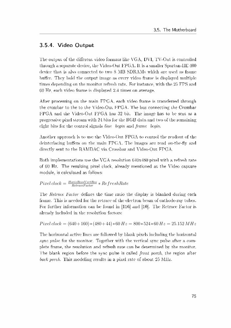
3.5. The Motherboard
3.5.4. Video Output
The output of the di�erent video formats like VGA, DVI, TV-Out is controlled
through a separate device, the Video-Out FPGA. It is a smaller Spartan-IIE 400
device that is also connected to two 8 MB SDRAMs which are used as frame
bu�er. They hold the output image as every video frame is displayed multiple
times depending on the monitor refresh rate. For instance, with the 25 FPS and
60 Hz, each video frame is displayed 2.4 times on average.
After processing on the main FPGA, each video frame is transferred through
the crossbar to the to the Video-Out FPGA. The bus connecting the Crossbar
FPGA and the Video-Out FPGA has 32 bit. The image has to be sent as a
progressive pixel stream with 24 bits for the RGB data and two of the remaining
eight bits for the control signals line_begin and frame_begin.
Another approach is to use the Video-Out FPGA to control the readout of the
deinterlacing bu�ers on the main FPGA. The images are read on-the-�y and
directly sent to the RAMDAC via Crossbar and Video-Out FPGA.
Both implementations use the VGA resolution 640x480 pixel with a refresh rate
of 60 Hz. The resulting pixel clock, already mentioned at the Video capture
module, is calculated as follows:
Pixel clock = HorizRes∗V ertResRetraceFactor
∗RefreshRate
The Retrace Factor de�nes the time ratio the display is blanked during each
frame. This is needed for the retrace of the electron beam of cathode-ray tubes.
For further information can be found in [116] and [10]. The Retrace Factor is
already included in the resolution factors:
Pixel clock = (640+160)∗(480+44)∗60Hz = 800∗524∗60Hz = 25.152MHz
The horizontal active lines are followed by blank pixels including the horizontal
sync pulse for the monitor. Together with the vertical sync pulse after a com-
plete frame, the resolution and refresh rate can be determined by the monitor.
The blank region before the sync pulse is called front porch, the region after
back porch. This modeling results in a pixel rate of about 25 MHz.
75

3. The Erlangen Slot Machine
76

4. Development of Partially
Recon�gurable Modules
4.1. Introduction
This chapter will describe the supporting framework for the ESM platform [45].
The goal is to automate the development process and to provide tested and
reusable hardware and software interfaces for application developers. Moreover,
the framework provides a guideline how to develop a hardware design that takes
advantage of partial recon�guration modules (PRMs) [21].
In the �rst part of the chapter, the standard design �ow for partial bitstream
generation will be described. In its current form the partial design �ow from
Xilinx [21] is based on a shell script that controls the partial module generation
after synthesis. This script assumes that the hardware design has been already
transformed to a partial design and is synthesized. However, most hardware de-
signs are not written with partial recon�guration in mind and the transformation
process for the communication with a partial module requires the insertion of
special macros into the top-level HDL design. In this case the top-level design
�le has to be rewritten. The result is an extensive code rewrite of the top-level
design �le. Moreover, partial design �ow speci�c rules and constraints must
be implemented. The chance for manual errors is high during this process, as
many new signals and constraints are introduced during this process. Based on
this experience, the transformation of a standard design into a partial design
can be automated. This idea resulted in the so-called SlotComposer tool that
77

4. Development of Partially Recon�gurable Modules
transforms a standard design into a partial design and generates an automated
partial design �ow for this project. The second part of this chapter describes
SlotComposer's automated design �ow.
After the bitstream generation, partial recon�guration modules must be stored
in local memory on the recon�gurable platform. Then each module can be
loaded on demand or according to a given schedule into the FPGA. The control
of the recon�guration process as well as module storage handling is implemented
in an operating system framework which is presented in the third part of this
chapter. The basis of the operating system framework is an embedded Linux
on the PowerPC microprocessor. The open source approach allows to take ad-
vantage of existing drivers for various peripheral devices. This is an important
feature as the ESM's Ethernet and USB interface chips are not directly sup-
ported by the embedded Linux [112, 113] distribution used.
Another important feature of the operating system framework is to provide
standard software APIs for software modules to connect to the underlying hard-
ware. These APIs include the Linux drivers for low level hardware access and
a standard library for communication and recon�guration control. Based on
these APIs, core operating system functions like �oorplanning and scheduling
of FPGA slots can be implemented. Having C-based libraries mandates an edit
and compile �ow for any changes made to the software application that is not
suitable for interactive testing. For debugging purposes an interactive shell ap-
plication was implemented. It allows to invoke all API functions directly from
the command line of a terminal session. As the main operating system is an
embedded Linux OS with full network connectivity, this interactive shell allows
to control and test partial recon�guration modules even from a remote host.
In the last part of this chapter we will describe a platform-independent bench-
mark approach for partial recon�guration. The goal is to build a methodology
that allows to measure the operating system's overhead during partial recon�g-
uration. We present a generic and customizable concept for the development
and prototyping of dynamically recon�gurable hardware tasks that allows to
study and compare di�erent scheduling and allocation techniques on di�erent
FPGA-based platforms.
78

4.2. Partial Design Flow
4.2. Partial Design Flow
To implement a partial recon�guration design successfully, you have to follow
a strict design methodology presented by Xilinx [21]. The guidelines to follow
are:
• Insert bus-macros between modules that need to be swapped out (called
partial recon�guration modules, or PRMs) and the rest of the design
(static logic).
• Follow synthesis guidelines to generate a partially recon�gurable netlist.
• Floorplan the PR Modules and cluster all static modules.
• Place all in and out signals of a PR Module in bus-macros.
• Follow PR speci�c design rule.
• Run the partial recon�guration implementation �ow.
To illustrate the di�erence between the static base region and the Partially
Recon�gurable Regions (PRR) a simple partial design is shown in Figure 4.1.
The base or static region is the portion of design that does not change during
the partial recon�guration process.
FPGA
PRR A
PRM A1
PRM A2
PartialBitstream A1.bit
PartialBitstream A2.bit
PRM A3 PartialBitstream A3.bit
Base Region
Figure 4.1.: Partial recon�gurable design with a single partial recon�gurable re-gion, PR Region A. Partial recon�guration modules PRM A1, A2,A3 can be loaded into PR Region A. All PRMs of the same PRRegion must have the same communication interface but there areno constraints on what logic is implemented inside the module.
79

4. Development of Partially Recon�gurable Modules
PR regions contain logic that can be recon�gured independently of the base
region and other partial recon�gurable regions. This logic is called Partial Re-
con�gurable Module (PRM). The shape, size and location of each PR region is
de�ned by the user through a range constraint. Each PR region has one, usually
multiple partially recon�gurable modules (PRMs) that can be loaded into the
corresponding PR region and share the same communication interface. Each
partial module is designed and implemented separately using the partial design
�ow. The slot terminology used with the ESM architecture refers to a partial
recon�gurable region. Similarly, the term hardware task or module refers to a
partial recon�guration module.
In application note 290 [105] Xilinx presents the design �ow for building recon-
�gurable designs based on their Modular Design. This �ow allows the recon-
�guration of entire columns of Con�gurable Logic Blocks (CLB) and does not
support static routes through recon�gurable areas. In a new version of the PR
design �ow [21] recon�gurable modules may span any rectangular area of an
FPGA and static routing can pass through recon�gurable modules.
The design �ow for partial recon�guration is shown in Figure 4.2 and consists
of several steps:
• First the HDL design description has to divided into static and partial
logic. The top design can only contain signals, bus-macros, I/Os, clock
primitives, static and partial module instantiations. No static logic is
allowed inside the top design. All input and output signals of a partial
module must pass through a bus-macro.
• In the second step design constraints are set for place and route. In ad-
dition to timing constraints PR designs mus be constrained with Area
Group, Area Group range, Location and Mode constraints. The Area
Group constraints must be de�ned for each recon�gurable region and for
the static part of the design. They separate clearly the static design form
the logic inside PR Modules. The Area Group range constraints de�ne
the shape/size and position for each recon�gurable region. The Mode
constraint must be also set for each recon�gurable region to prevent un-
expanded block errors during base and PR module implementation. The
Location (LOC) constraint must be set for all I/O pin clock primitives and
bus-macros. Bus-macros must be located so that they touch the boundary
between the PR region and the base design.
80

4.2. Partial Design Flow
• The third step in the PR design �ow is not required but is recommended
before moving to the PR design implementation. This step implements
the design in the non-PR �ow and is important for placement analysis. It
helps to determine the best Area Group range and bus-macro locations.
The Mode constraint should be removed during this step.
• The next step is to analyze both the timing and placement of the design.
This analysis is needed to establish the best PR region shape, size and lo-
cation. Timing analysis is used to �nd paths that fail the constraints. This
can happen due to not optimal location or shape of the PR region. Wrong
or not e�ective bus-macro placement is also often a source of problems.
• In step �ve the base design is implemented. During base design implemen-
tation, the synthesized top-level of the design is merged with the static
part of the design and a static.used �le is generated. This �le contains a
list of routes within the PR regions that cannot be used by PR modules
because they are required by the static part of the base design.
• The sixth step implements PR modules separately within its own directory
hierarchy. If the static.used �le changes, then each PR modules must be
reimplemented.
• In the �nal PR design �ow step the top, static and partial modules are
merged to build the complete design. Partial bitstreams are created for
each PR module and one full bitstream for the PR module merged with
the base design.
The standard approach to the partial recon�guration design �ow is to write a
script �le that implements all steps. The second constraint step will always
remain manual, as it speci�es designers input.
A partial automation of the XILINX design �ow can be achieved with the hi-
erarchical �oorplanning and design tool PlanAhead [106, 117, 118, 28]. The
PlanAhead software has a graphical user interface that allows to de�ne and
change the size and shape of the partial modules. It allows also to change the
placement of internal FPGA resource, like registers or BlockRAMs, when timing
constraints are not met because of timing violations caused by partial module
boundaries. Additionally, PlanAhead performs automatic design rule checking
and can generate a partial bitstream for the design.
81
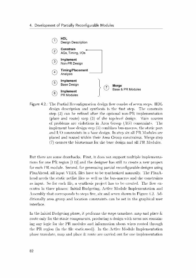
4. Development of Partially Recon�gurable Modules
Figure 4.2.: The Partial Recon�guration design �ow consist of seven steps. HDLdesign description and synthesis is the �rst step. The constrainstep (2) can be re�ned after the optional non-PR implementation(place and route) step (3) of the top-level design. Main sourcesof problems are violations in Area Group (AG) constraints. Theimplement base design step (5) combines bus-macros, the static partand I/O constraints in a base design. In step six all PR Modules areplaced and routed within their Area Group constraints. Merge step(7) creates the bitstreams for the base design and all PR Modules.
But there are some drawbacks. First, it does not support multiple implementa-
tions for one PR region [119] and the designer has still to create a new project
for each PR module. Second, for generating partial recon�gurable designs using
PlanAhead, all input VHDL �les have to be synthesized manually. The PlanA-
head needs the static netlist �les as well as the bus-macros and the constraints
as input. So for each �le, a synthesis project has to be created. The �ow ex-
ecutes in three phases: Initial Budgeting, Active Module Implementation and
Assembly that corresponds to steps �ve, six and seven shown in Figure 4.2. Ad-
ditionally area group and location constraints can be set in the graphical user
interface.
In the Initial Budgeting phase, it performs the steps translate, map and place &
route only for the static components, producing a design with areas not contain-
ing any logic for the PR modules and information about wires routed through
the PR region (in the �le static.used). In the Active Module Implementation
phase translate, map and place & route are carried out for one implementation
82
4.3. The SlotComposer
of each PR region. In a �nal step, the Assembly phase, the PR modules are
merged and the bitstreams are generated. To produce more than one bitstream
for a PR region, another PlanAhead project containing one set of not yet im-
plemented PR modules has to be created. Additionally, the static.used �le has
to be manually copied into the project.
Using scripts or PlanAhead for the automation of the partial recon�guration
�ow is a good idea. However, both approaches do not provide any support in
the HDL design or constrain step. The HDL design for PR design �ow requires
explicit insertion of bus-macros in the HDL top-level �le. Writing design that
contain several PR modules with many input/output signals will require the in-
stantiation of many bus-macros and even more intermediate signals. Moreover,
all bus-macros must be constrained to a correct location. Our experience has
shown that these steps are time consuming and a source of placement errors.
4.3. The SlotComposer
SlotComposer is a tool developed for an automated bitstream generation of
partial modules. Moreover, SlotComposer converts a standard VHDL design
to a partial design by modifying the top-level design �le and by generating
new constraint �les for the PR design �ow. Then it generates all design �ow
scripts and infrastructure to generate standard and partial bitstreams. Using
the existing Xilinx Partial Recon�guration Tool Flow, SlotComposer inserts
bus-macros between each input and output signal of a partial module. Its user
interface is depicted in Figures 4.4 and 4.5.
Based on users speci�cation SlotComposer can also connect partially recon�g-
urable modules to the Recon�gurable Multiple Bus or the Crossbar interface. At
the same time it generates all necessary constraint �les and optimizes the usage
and placement of bus-macros. Moreover, all required scripts for the synthesis of
all components and the PR-Flow are generated, as shown in Figure 4.3.
To use the PR-Flow from Xilinx, the hardware design has to follow a speci�c
�le structure. The top-level design �le instantiates the static and all partial
recon�guration modules (PRMs), global logic, I/O-Ports and clock primitives.
Furthermore, the top-level design �le also describes the inter-module communi-
cation pattern. SlotComposer eases the transformation to the PR design �ow
83

4. Development of Partially Recon�gurable Modules
by an automated instantiation of the communication structures in the top-level
HDL design �le.
SlotComposer
1) Insertion of bus-macrosin top level VHDL
2) Partial Region shapeextension
3) Location of bus-macros
4) Creation of projectdirectory structure
5) Generation of designflow scripts
New constraint file
New top level design file
Partial and basebitstreams
PR Modules, Top level design,Constraint file, bus macros
Figure 4.3.: Based on a modular design SlotComposer automatically inserts andplaces bus-macros inside the top-level VHDL design. Bus-macrosare correctly connected in between static and partial modules. Theshape of a partial module can be changed to create valid locationsfor bus-macros. Then a new project directory structure is createdtogether with the partial design script for partial and base bitstreamgeneration.
To minimize the number of resources SlotComposer packs as many signals into
a bus-macros as possible. As bus-macros can only be placed between adja-
cent modules, SlotComposer can adjust the placement of modules to meet this
requirement. If the boundary between two neighboring modules is not long
enough to insert all required bus-macros, SlotComposer can change the size of
the recon�gurable region to satisfy this condition and modi�es the UCF �le.
Special tags have to be included as a comment in the HDL �le for SlotComposer
to recognize the partial recon�gurable regions. For example, if the design has
two recon�gurable area groups then the label '� PR Module 1 ' is inserted before
component instantiation of the partial module for the �rst recon�gurable area
84

4.3. The SlotComposer
group and '� PR Module 2 ' before the module for the second area group. In
order to instantiate the correct bus-macros in the top-level design the position
of each area group must be provided in the UCF �le.
Figure 4.4.: SlotComposer application allows to convert modular VHDL designsinto partial designs. After the selection of the project directory, userconstraints �le, FPGA device type and bus-macros the project canbe converted to adhere to the PR design �ow.
As the PR Flow is de�ned by Xilinx and subject to further changes the Slot-
Composer uses a template engine for the generation of the PR �ow scripts. If
changes are to appear in the PR �ow then only the template �les for the partial
design �ow must be changed and not the tool itself.
SlotComposer was tested successfully with three modular applications without
bus-macros. Bus-macros were automatically inserted in the top-level VHDL �le.
The generated PR �ow script successfully built all partial and static bitstreams.
These applications included:
• XUP Color Counter is a demo project for Xilinx XUP Virtex II Pro De-
velopment System [120]. The Color Counter application consists of �ve
85

4. Development of Partially Recon�gurable Modules
static modules, each of them with its own Area Group property, and one
partially recon�gurable region with two di�erent partially recon�gurable
modules. The recon�gurable region is connected to one of the static mod-
ules via three horizontal bus-macros.
• The second design uses the Recon�gurable Multiple Bus (RMB) as a com-
munication interface among four partially recon�gurable regions. Each
region has one recon�gurable module. Each of the recon�gurable regions
is connected to the RMB via a group of vertical bus-macros.
• Video �lter is an ESM application composed of a static part and one
PR region with partially recon�gurable �lter modules. The PR region
has an Area Group property, while the static part of the design can be
speci�ed either with an AG property or without. When the static part of
the design has no area group property then bus-macros are placed on the
left boundary of the recon�gurable region. The static Area Group range
is created in the lower left corner of the FPGA device and extended in
horizontal and vertical direction until touching the PR region. All bus-
macros are then placed on the boundary.
4.4. Operating System Framework
Hardware tasks denote partially recon�gurable modules with an additional con-
trol interface. The Operating System Framework implements a working envi-
ronment for the development of hardware tasks. It builds an abstraction layer
hierarchy for software as well as hardware application development on the ESM
platform. Operating system tasks like partial module instantiation, run-time
module relocation, recon�guration scheduling, and inter-module communica-
tion management can be implemented on a microprocessor, as these tasks are
control oriented and have a low computational density. A hardware implementa-
tion of the operating system is possible but it lacks run-time �exibility, occupies
valuable hardware resources and provides no substantial performance bene�t.
Managing partial modules on the FPGA, con�guration data, module execution
requests is performed in software. The corresponding functionality of the ESM
software framework is depicted in Figure 4.6. The ESM Motherboard and the
ESM Babyboard are the basis for this Operating System Framework [49]. On
86

4.4. Operating System Framework
Figure 4.5.: SlotComposer application allows to convert modular VHDL designsinto partial designs. This window of SlotComposer shows one staticmodule on the left and three partial modules on the right side. Bus-macros are shown as small boxes connecting these modules together.The absolute placement of bus-macros and all modules is representedby the grid position measured in slices.
top of the ESM boards hardware designs or �rmware for the recon�guration
manager, crossbar and hardware task framework are implemented. They are
loaded only once but can be easily replaced by variants during system start-up.
The recon�guration manager, as described in Section 3.4.2, is implemented as
a custom MicroBlaze architecture containing modular accelerators for memory
transfers, bit�le reallocation and con�guration management. The crossbar mod-
ule is responsible for the communication between Motherboard and Babyboard
as well as for control of FPGA's I/O connections to peripheral devices like video
and audio I/O. Partial recon�guration modules or hardware application tasks
are built upon the hardware task framework and represent the run-time adapt-
able part of an application. The hardware task framework provides a control
interface in hardware for each partially recon�gurable module (PRM). Each
PRM that implements this control interface is called a hardware task.
The software layer consists of the Linux Kernel drivers at the bottom and is
87

4. Development of Partially Recon�gurable Modules
ESM Platform: Virtex-II FPGA, Crossbar FPGA, External I/O Devices
ReconfigurationManager HW-Module Crossbar HW-Module
Hardware Task Framework
ESM Devices Layer (ESMDL)
Scheduling & Placement Framework
ESM Shell Custom Scheduler & Placer
HardwareTasks
Reconfigurable Application
Figure 4.6.: Firmware stack developed for the Erlangen Slot Machine. A recon-�gurable application running on the ESM includes a custom sched-uler and placer as well as a pool of hardware tasks. Hardware tasksare partially recon�gurable modules with an additional control in-terface.
built around a modi�ed version of the DENX ELDK Linux 2.4 kernel [112] and
U-Boot bootloader [113]. The Linux kernel drivers are responsible for low level
hardware communication with the crossbar through the use of memory mapped
I/Os. They also store and manage the current status of the crossbar and the
recon�guration manager. The software API is based on these Linux kernel
drivers and is a C-based library containing scheduling, placement, hardware
recon�guration and management functions for the ESM platform.
The crossbar provides multiple communication channels for any kind of data
transfer between the main FPGA one side and the PowerPC microprocessor or
peripheral devices on the other side.
For testing purposes a shell like application has been created. This ESM-Shell
encapsulates the C-based API functions into scriptable commands analog to the
Bash-Shell. This opens up the possibility for shell script based testing or the
direct manipulation of the ESM system during run-time.
88

4.4. Operating System Framework
The �rst group of ESM shell commands is used to set or reset internal crossbar
connections. Before a partial module is loaded into the main FPGA all for the
new partial module relevant I/O connections must be set. All functions available
in the ESM shell are also implemented in the software API of the middleware
layer.
• pin_connect connectionlist : connect all pins in the list (example: pin_connect
D1-VGAB1 D2-VGAB2 D3-VGAB3 D4-VGAB4)
• pin_disconnect connectionlist : disconnect all pins in the list (example: pin_disconnect
D1-VGAB1 D2-VGAB2 D3-VGAB3 D4-VGAB4)
• get_pin_connections: returns a list of all connected pins with connection part-
ners
• reset_crossbar : delete all crossbar connections.
The second group of ESM shell commands implements basic recon�guration
management functions.
• rcm_write_�ash address [length] bit�le: write a bit�le to �ash memory at ad-
dress address. Length de�nition is optional.
• rcm_write_fpga bit�le: write a bit�le directly to FPGA.
• rcm_write_fpga_from_�ash address length: write a bitstream located at �ash
position address an length bytes long to FPGA.
• rcm_read_�ash address length bit�le: read length bytes of �ash memory at
address address and write it to �le bit�le.
• rcm_write_�ash_reloc address [length] bit�le reloc_o�set : write a bit�le to
�ash memory at address address and relocate it by reloc_o�set. Length de�ni-
tion is optional.
• rcm_write_fpga_reloc bit�le reloc_o�set: write a bit�le directly to FPGA and
relocate it by reloc_o�set.
• rcm_write_fpga_from_�ash_reloc address length reloc_o�set : write a bitstream
located at �ash position address and length bytes long to FPGA and relocate
it by reloc_o�set.
89

4. Development of Partially Recon�gurable Modules
• rcm_read_�ash_reloc address length bit�le reloc_o�set : read length bytes of
�ash memory at address address, relocate it by reloc_o�set and write it to �le
bit�le.
• rcm_erase_�ash_block address length: erase �ash block(s) beginning at address
for length byte.
• rcm_reset_modules FLASH|FPGA|FLASH_AND_FPGA: resets either the �ash
module of the rcm, the FPGA module or both.
• rcm_read_status: print status information of the RCM.
The last group of commands can be used to size up and write register of the
crossbar communication interface. They are useful to verify the currently used
communication settings between the crossbar and the PowerPC microprocessor.
• hwswcom_setbit bytenumber bitnumber : set bit bitnumber in byte bytenumber
in Hardware-Software-Communication memory (intention: set input to FPGA
pins to 1).
• hwswcom_clearbit bytenumber bitnumber : clear bit bitnumber in byte bytenum-
ber in Hardware-Software-Communication memory (intention: set input to FPGA
pins to 0).
• hwswcom_getbit bytenumber bitnumber : check if bit bitnumber in byte bytenum-
ber in Hardware-Software-Communication memory is set .
4.5. Real-time Recon�gurable Hardware Task
Management
To demonstrate the bene�t of partial recon�guration for real applications, the
development of special operating system concepts is necessary in order to ad-
dress the peculiarities of modularization, inter-module communication, recon-
�guration scheduling and time-dependent allocation of resources with respect
to di�erent, often also real-time constraints. Unfortunately, research work so
far does not consider or re�ect the real underlying hardware and works just on
�ctive numbers or abstract mathematical models of hardware tasks, respectively
module parameters.
90

4.5. Real-time Recon�gurable Hardware Task Management
We present a methodology for generating a synthetic benchmark for dynamically
recon�gurable hardware task bitstreams parameterizable in a) module size, b)
execution time, c) arrival time, and d) possibly deadline, as well as a methodol-
ogy for wrapping and modularizing arbitrary user hardware modules into such
�exible callable and loadable module concept for di�erent FPGA platforms.
A scripted tool supporting the generation of such modules makes the generation
of dynamic hardware task easier and research on recon�guration scheduling and
allocation more comparable.
In the real-time machine scheduling and embedded systems research community,
Dick et al. have reached a big breakthrough with their 1998 seminal paper
TGFF [121]: Task Graphs for Free o�ering a user-controllable, general-purpose
generator of synthetic software task graphs that is heavily used in the real-
time scheduling research ans system synthesis areas. The bene�t of such a
benchmark concept is that by sharing of parameter settings, researchers may
easily reproduce examples and case studies used by others, regardless of the
platform.
The intention is to provide a similar concept and methodology also for the do-
main of recon�gurable computing on FPGAs. In particular, we present a generic
and customizable concept for the development and prototyping of dynamically
recon�gurable hardware tasks that allow us to study and compare di�erent
scheduling and allocation techniques on di�erent FPGA-based platforms in a
reproducible manner. With this respect, we present
• a methodology for generating synthetic benchmarks for dynamically re-
con�gurable hardware task bitstreams parameterizable in
� arrival time,
� (core) execution time,
� recon�guration time (indirectly through speci�cation of module size),
and
� deadline, as well as
• a methodology for wrapping and modularizing arbitrary user hardware
modules into such �exible callable and loadable module concept for dif-
ferent FPGA platforms. The goal is to make dynamic hardware task
91
4. Development of Partially Recon�gurable Modules
generation a part of our methodology to support automated generation of
such callable and freely relocatable partial bitstreams.
In the following, we present an environment for the generation of partially re-
con�gurable tasks suitable for benchmarking. We assume that a recon�gurable
system consists of a recon�gurable device which is linked via a hardware ab-
straction layer to an operating system. The operating system layer contains a
task scheduler and a placer as well as a recon�guration manager connected to a
task repository. The task scheduler decides a starting time for each task, based
on an application speci�c scheduling policy. Figure 4.6 presents an abstracted
view of such a recon�gurable system. An o�-line schedule is suitable for stati-
cally de�ned applications, whereas on-line schedulers are suitable for problems
with dynamic, i.e., event-based computation requests. The placer keeps track
of all run-time assigned resources and initiates loading and unloading of tasks,
based on the scheduler output, via the recon�guration manager.
The recon�guration manager is responsible for storage and caching of bitstreams
which represent di�erent hardware modules. Caching of bitstreams in SRAMs
or fast Flash memory devices allows the operating system to decrease the re-
con�guration time for each hardware module load process.
The aim is to physically measure the start to end execution time of a task and
to compare them with simulation results across a wide range of recon�gurable
platforms. We propose an automated generation of generic and con�gurable
hardware tasks for this purpose.
Hardware tasks are partially recon�gurable modules with an additional control
interface. As shown in Figure 4.6, a recon�gurable application running on the
ESM includes a custom scheduler and placer as well as a pool of hardware tasks.
In our approach, each hardware task (module) i is parametrized by the following
attributes: arrival time Ai, start time Si, enable signal Ei, recon�guration time
Ri, and core execution time Ci. The arrival time Ai is the time at which the
request for the execution of a module becomes known to the recon�guration
manager. If an empty slot is found on the FPGA device for the requested
task, then the start time Si denotes the beginning of the partial recon�guration
process for this task. The recon�guration time Ri itself depends on the size of
the bitstream being loaded, the speed of the recon�guration interface, and the
software overhead in the operating system layer. Figure 4.7 shows the time scale
of events.
92

4.5. Real-time Recon�gurable Hardware Task Management
Figure 4.7.: Time line showing the arrival of a task request, its recon�gurationand execution time. The execution is enabled separately throughthe enable signal Ei. An example of an active device supportingpartial recon�guration at run-time is shown in Figure 1 c).
The operating system layer implements a basic set of software functions needed
for running these benchmarks. These functions must include bitstream loading
operations as well as reset, setState and getState functions for each partial mod-
ule. The setState and getState are for control and monitoring of the hardware
task state. The life cycle of each task consists of �ve states, such as not active,
scheduled, loaded, running and idle. The state diagram in Figure 4.8 shows the
life cycle of a hardware task.
not active
idle
running
loaded
scheduled
reconf igure S_i
enable E_i
not done
done
enable E_i
remove Z_i
no request
request A_i
FSM Version 1.26/17/2010 10:11:13 PM
Figure 4.8.: State diagram showing the life cycle of a hardware task.
93
4. Development of Partially Recon�gurable Modules
As long as a hardware task is not loaded it resides in the default not active
state. To remove a hardware task the partial recon�guration region is reloaded
with a blank module. An example time line of events is shown in Figure 4.7.
4.5.1. Hardware Task Generation
We implemented the generation of partially recon�gurable hardware tasks in
the so called design tool hwtaskgen which generates partially recon�gurable
VHDL tasks. In order to test scheduling and allocation algorithms all task have
common interface which is a must for partial recon�guration.
Synthetic hardware task generation is the main mode for the generation of
reusable hardware modules. In this mode, a task set of concurrently running
hardware modules can be generated. No overlapping in the placement is allowed,
as this would generate errors during the place and route phase of the design. If
a big task set of modules has to be generated that does not �t physically on the
device, then several independent task sets have to be created. This set is also
necessary if run-time relocation of modules is not implemented in the operating
system layer. In this case, di�erent module placements can be implemented for
one task set if possible. Otherwise, additional task sets have to be created.
In the second wrapper mode, existing hardware modules may be wrapped by a
hardware interface that includes a communication interface for the operating
system to create a partially recon�gurable hardware task. In this case the hard-
ware module interface is extended by a few signals necessary for benchmarking
purposes. The original module interface is not changed. In particular, this
concept holds for any hardware modules that perform a function evaluation.
Figure 4.9 presents a view of a recon�gurable device populated with a generated
synthetic benchmark set with three hardware tasks (HW-T1, HW-T2, and HW-
T3). Each hardware task is connected via Xilinx speci�c bus-macros to the
static part of the design. All hardware tasks are run-time recon�gurable while
the static part runs uninterrupted during the recon�guration process. Each
task has its own I/O interface including two additional control signals. The
enable signal is set by the operating system layer after the hardware module has
been successfully loaded. It enables the execution if set, otherwise execution is
disabled. The done output signal is set once the task execution is �nished.
94

4.5. Real-time Recon�gurable Hardware Task Management
Figure 4.9.: Generated hardware task set consisting of three modules (HW-T1,HW-T2, HW-T3) with di�erent module widths. All signals betweenthe static part and modules pass through bus-macros.
4.5.2. Design Flow
Our design �ow is based on the Xilinx Early Access Partial Recon�guration
(EAPR) Flow [21] that supports the creation of partial hardware modules. Using
EAPR requires the creation of one static module where all partial modules are
connected to, as shown Figure 4.9. This means that all signals of any partial
module connected to external pins have to go through the static part of the
design. The standard method for communication is using bus-macros which
connect partial modules with the static part of the design and can also be used
for inter-module communication.
The design �ow for partially recon�gurable real-time task is composed of three
main parts, namely
• partial hardware module creation, including module allocation, recon�gu-
ration, and scheduling, and a
• operating system layer running on a Soft- or Hardcore CPU,
95
4. Development of Partially Recon�gurable Modules
• HW-SW interface between hardware modules and the operating system
layer.
This operating system layer is build on top of a hardware abstraction layer
which encapsulates the HW-SW interface. In its implemented form, the HW-
SW interface contains only a memory mapped register set. This register set is
used by the hardware modules and the PowerPC microprocessor to read and
update status information of each hardware task.
Software API The scheduling environment consists software library that in-
cludes all platform speci�c functions to manage the execution of partial re-
con�gurable hardware tasks on the FPGA. The device independent part, such
as scheduling and placement algorithms, are integrated into a Hardware Task
Scheduler software library. This library can be reused on other platforms as
long as a similar software library is available on the target's microprocessor.
In more detail, the software library includes functions to manage bitstreams in
a module cache, if a cache memory is supported on the recon�gurable platform.
The addToModuleCache and the removeToModuleCache functions can be used
to add new bit�les and remove existing �les from the cache memory, respectively.
The listModuleCache command can be called to receive a list of all bitstreams
currently available in the module cache. A call to resetModuleCache clears the
content of the whole module cache by removing all modules.
The most important function is loadModule, which loads a given bitstream on
the main FPGA at the given position. If the partial module is available in the
module cache, then the bitstream is loaded from there into the main FPGA.
Otherwise, the bitstream has to be transferred from an external source, for
example a network directory, to the main FPGA. This operation can last for
some time and should be avoided by storing partial module bitstream in the
cache memory up-front. The unloadAllModules function can be called to reset
the FPGA and remove all modules placed on the recon�gurable hardware.
1 // Module Cache Routines
2 int addToModuleCache ( s t r i n g b i t f i l eName ) ;
3 int removeFromModuleCache ( s t r i n g b i t f i l eName ) ;
4 l i s t l i stModuleCache ( ) ;
5 int resetModuleCache ( ) ;
6
7 // Recon f i gura t ion Routines
96

4.5. Real-time Recon�gurable Hardware Task Management
8 int loadModule ( s t r i n g b i t f i l e , int po s i t i o n ) ;
9 int re se tAl lModule s ( ) ;
10
11 // Module S ta t e Routines
12 moduleStates getModuleState ( int pos i t i on , optionalStateToWaitFor ) ;
13 int setModuleState ( int pos i t i on , moduleStates va lue ) ;
Listing 4.1: Summary of used software library functions supported by the oper-
ating system layer.
Additionally, two more functions are used to control a hardware task. The
getModuleState routine can be called to poll if a loaded module at a speci�ed
position has �nished its execution or is still running. Optionally, a second
parameter can be speci�ed. In this case, the function does not return until the
task entered the corresponding state. The setModuleState function is used to
set the task state. In particular, the execution of a running task can be stopped
and periodic tasks can be activated or deactivated at speci�ed times. As a side
e�ect this allows to time-multiplex running modules on the main FPGA.
Evaluation of Recon�guration Overheads To optimally schedule a set of
tasks on a recon�gurable platform, the recon�guration time overhead must be
carefully studied and taken into account. The recon�guration overhead for a
hardware task determines whether dynamic hardware recon�guration makes
sense at all for certain applications. Therefore, we developed a measurement
software which loads hardware tasks bitstream of di�erent module sizesWi (slot
widths in CLBs) and known core execution times Ci, each at a time on the main
FPGA. The software measures the time form the point when the loadModule
command is issued in software to the point where the getModuleState command
returns that the module is loaded and ready. This way, the recon�guration time
overheads caused by a) the software layer, b) by transferring the bitstream from
the module cache or from the memory of the control CPU, and c) the actual
loading on the FPGA are quantitatively determined. For the ESM platform the
Figure 4.10 and Table 4.1 show these recon�guration times Ri depending on
the size of the module to be loaded. For example, modules with the width of
8 CLBs are recon�gured in 127 ms. In all cases, the software overhead for the
recon�guration was measured with 3 ms. The same measurement strategy can
be used on other platforms as long as a similar software library is available.
97

4. Development of Partially Recon�gurable Modules
Hardware task width in CLBs Recon�guration time in ms
4 978 12712 16824 33236 48448 67360 83772 1013
Table 4.1.: Recon�guration overhead on the ESM platform for di�erently sizedpartial modules. All hardware tasks are loaded from �ash memorydirectly into the main FPGA. The software overhead is very smallbecause only one command has to be sent to the Recon�gurationManager to load a partial module from �ash memory.
0 12 24 36 48 60 720
200
400
600
800
1000
Reconfigurable module width in CLBs
Rec
onfig
urat
ion
tim in
ms
Figure 4.10.: Measured recon�guration times for generated hardware tasks withdi�erent module widths. Hereby, a constant time overhead of 3 mswas resulting from the software layer.
Task Scheduling To measure the recon�guration overhead and to compare
it with the theoretical value, ten independent tasks are generated. In the next
step, a schedule minimizing the makespan of the task set must be found. All ten
hardware tasks have the same width of 8 CLB columns and can be loaded into
any of the six available slots on the FPGA. Each task's core execution time is a
98

4.5. Real-time Recon�gurable Hardware Task Management
multiple of the measured recon�guration time of 127 ms. This is the same time
required for the partial recon�guration of an 8 CLB wide hardware task. Either
an on-line scheduling algorithm based on software library functions may be used
or an o�-line scheduling algorithm may be run. In our example, we decided on
the latter approach in order to determine the optimal schedule for the example
problem. Furthermore, currently available FPGAs have the limitation, that just
one task can be recon�gured at the same time. This additional recon�guration
constraint must be taken into account. Our optimal schedule minimizes the
makespan while respecting the recon�guration overheads, as shown in Figure
4.11. Hereby, tasks 3, 5, 1, 6, 8, 9 can't start simultaneously because only one
task can be recon�gured at the same time. According to the theoretical schedule
results, the total execution time of these tasks on our recon�gurable platform
should be 24 ∗ 127ms = 3.048 s.
time steps
reco
nfig
urab
le s
lot p
ositi
on
Figure 4.11.: Schedule produced for the example problem by our scheduling sim-ulator. The brightly shaded rectangular areas stand for the recon-�guration times Ri, the green ones for the core execution timesCi.
The resulting schedule can be represented by a list of pairs in which the �rst
member speci�es the task index and the second the corresponding slot position
on the recon�gurable device. The �rst pair in the list speci�es the task to
be recon�gured �rst. For the example schedule in Figure 4.11, the schedule
list equals {(3, 1), (5, 2), (1, 3),(6, 4), (8, 5), (9, 6), (7, 2), (10, 5), (4, 1), (2, 3)}. A
loader function, see Listing 4.2, does the partial bitstream loading according to
99

4. Development of Partially Recon�gurable Modules
the slot position found earlier during scheduling. It �rst removes the �rst item of
the schedule list and checks if a module occupying the destination slot position
has �nished its execution. Only if the �ag Done is set the getModuleState
function terminates and the next hardware task can be loaded.
To generate the above example task set, our tool hwtaskgen was used. The
parameter is a list of triples containing the slot position pi of the hardware task
on the FPGA, width Wi and the execution time C. An example parameter list
for n tasks looks as follows: {(p1,W1, C1), (p2,W2, C2), ..., (pn,Wn, Cn)}.
1 l oade r ( Pa i rL i s t l i s t S c h e du l e )
2 {
3 while (0 < l i s t S c h e du l e . s i z e ( ) ) {
4 nextPair = l i s t S c h e du l e . removeFirst ( ) ;
5 nextTaskIndex = nextPair . index ( ) ;
6 nextTaskPos = nextPair . p o s i t i o n ( ) ;
7 i f ( getModuleState ( nextTaskPos , DONE) {
8 loadModule ( b i t f i l eName [ nextTaskIndex ] , nextTaskPos ) ;
9 }
10 }
11 }
Listing 4.2: Loader function to recon�gure the hardware tasks according to an
o�-line schedule.
For the above example task set, a total execution time on the real physical
hardware was o� by only 3.67 %. In particular, the measured time for the
makespan of this task set was 3160ms versus 3048ms for the optimal execution
time of all ten tasks. The di�erence between theoretical and experimental results
may be further reduced by improving the deterministic behavior of our hardware
and software implementations. Our embedded Linux kernel [112] does not use
any real-time extension, that would allow a more deterministic software IRQs.
The operating system overhead for task scheduling approaches can have a signif-
icant impact on the makespan performance of a executed task set. Our analysis
and comparison of scheduling simulation and a physical task set execution on
our platform demonstrated that the operating system impact on the makespan
performance was below 6.04 % or 3 ms. It must be noted that the results were
achieved on the ESM platform. However, with the hwtaskgen tool the same
task set can be generated for di�erent platforms. The main goal of this tool
is to encourage the comparison of recon�gurable platforms in terms of their
100

4.6. Hardware Interfaces for Video Processing
practical recon�guration performance and to reproduce examples used by other
researchers. Moreover, we presented a standard method for rapid generation of
synthetic, partially recon�gurable hardware task sets which enable the genera-
tion of scheduling benchmarks for various recon�gurable computing platforms.
4.6. Hardware Interfaces for Video Processing
In this section, components of the Erlangen Slot Machine important for video
processing will be highlighted. For the design of the hardware interfaces, the
application requirements placed on the whole system are considered.
4.6.1. Overview
The �rst step in implementing a video processing application on the ESM plat-
form is to provide video input and video output to the main FPGA which hosts
the hardware processing modules. Depending on the location of the recon�g-
urable regions, the crossbar has to switch the video input and video output to
the correct slot positions on the main FPGA. The resulting images are then
overlayed with visual guides before being displayed. To separate this task from
the video application an output frame bu�er is required. Displaying additional
information inside the video image is done by writing the information directly
into the frame bu�er. Modules processing the video stream on the main FPGA
need fast memory bu�ers to store the images for convolution and intermediate
results. Some of the algorithms can use a hardware-software co-design approach
by using the PowerPC for software computations, as shown in Figure 4.12. In
this case, the hardware-software communication must be additionally instanti-
ated to send and receive data from the software part of the application.
As an additional objective, the video processing modules must not occupy the
whole area of the main FPGA to allow other recon�gurable modules to run in
parallel. The aim is to demonstrate the ESM architecture's capability for paral-
lel computing as well as the support for partial recon�guration - reprogramming
logic cells while not interrupting the circuits of other parallel applications mod-
ules.
101

4. Development of Partially Recon�gurable Modules
Figure 4.12.: Simpli�ed structure of a video processing application designed forthe ESM platform. In its basic form, the video processing moduleis connected to an input and output module. These three mod-ules reside on the main FPGA and require external memory. Thecommunication to and from the main FPGA is controlled by theCrossbar FPGA.
The requirements for running a video processing application on the ESM plat-
form can be summarized as follows:
• an optimized video I/O system for VGA resolution of 640x480 pixels at
60 Hz,
• fast memory interfaces for bu�ering,
• hardware-software communication, and
• available resources on the main FPGA for other recon�gurable applica-
tions.
102

4.6. Hardware Interfaces for Video Processing
4.6.2. HW/SW Communication
The main FPGA and the PowerPC can only communicate via the crossbar. The
PowerPC is connected to the crossbar FPGA with its full 32 bit address and
data bus. The crossbar contains a register bank that is transparently mapped
into the address space of the PowerPC. Access to these registers is implemented
through standard memory read or write instructions. The software drivers are
implemented as Linux character device drivers. They control the access to
the crossbar register bank and are responsible for read and write access to the
memory mapped I/O registers. In order to ease the software interface, a custom
software library is provided. This library implements functions necessary for
sending or receiving whole data bu�ers to and from the main FPGA.
4.6.3. Video Input
The ESM o�ers an analog composite video input that is handled by the video
input module located inside the Crossbar FPGA. One question is to how to
deinterlace the incoming video frames. For the implementation of the deinter-
lacing scheme two options are possible. Either, the SDRAM at the crossbar
FPGA is used to deinterlace the image directly after the RGB conversion, or
the deinterlacing is implemented on the main FPGA. In this case, an SRAM
and some logic area of the main FPGA are utilized for deinterlacing.
As discussed in [10], a method for deinterlacing a video stream is the weave
mode. Here, the lines of both �elds are weaved into each other. With an output
frequency of this module fpair = 12.5MHz and the required VGA pixel clock
fpixel = 25MHz as well as the incoming video stream bit width wpair = 48 bit
and output bit width after the RGB conversion wRGB = 24 bit the throughput
of the deinterlacing node is speci�ed as follows:
Rdeinterlacing = fin ∗win +fout ∗wout = fpair ∗wpair +fpixel ∗wRGB = (12.5MHz ∗48 bit) + (25MHz ∗ 24 bit) = 600Mbps+ 600Mbps = 1.2Gbps
This data rate can be reduced by converting the color images to grayscale.
Hence, the data rate can be reduced to one third by converting 24 bit RGB
pixels to 8 bit grayscale pixels. The optimized video input has then the following
throughput requirements:
103

4. Development of Partially Recon�gurable Modules
R′deinterlacing = fin∗w′in+fout∗w′out = fpair∗wgraypair+fpixel∗wgray = (12.5MHz∗16 bit) + (25MHz ∗ 8 bit) = 400Mbps = 1/3Rdeinterlacing
The reduced throughput enables the overall realization of a video processing
pipeline, as memory has to be split among the subsystems.
4.6.4. Video Output
After passing the processing modules on the main FPGA, the images are sent
to the display frame bu�er on the Motherboard. The VGA output mode is set
by the Video-Out FPGA to 640x480 at 60 Hz. For simple video �lters the direct
output of the video stream can be implemented. For this to work, the processed
image bu�er must be read 60 times per second and the pixel stream has to be
passed through to the RAMDAC device. However, the start of a new image
on the VGA output is not synchronized with the output process of the video
processing module. This leads to visible image change, mainly during pan and
tilt of the camera, in the middle of the displayed image because the display of
the next image frame is not synchronize with the vertical sync signal. To avoid
this, the video images must be stored in a frame bu�er before being displayed
through the VGA.
A dedicated output logic is required to control the frame bu�er. Visual guides
implemented in hardware on the Video-Out FPGA can be used to draw addi-
tional information on top of the video images. They are merged with the video
stream resulting in a 24 bit RGB output for the VGA signal generation in the
RAMDAC device. Upon the �rst pixel of a frame a frame begin signal must
be set. The frame bu�er is implemented on the Video-Out FPGA and uses the
two 8 MByte SDRAMs.
4.6.5. Memory Interfaces
Video image processing requires access to large image memory. When convo-
lution �lters are applied on an image every pixel inside the sliding window has
to be accessed. The internal BlockRAM of an FPGA is good choice for stor-
ing images because it supports dual ported access. However, its size is limited
and a grayscale image of 640x480 pixels does not �t into the distributed RAM
104

4.6. Hardware Interfaces for Video Processing
of the complete FPGA. Hence, external memory bu�ers must be utilized. To
ful�ll the real-time conditions without skipping any frame, they must be fast
enough to accept incoming image data and at the same time output data for
the next process. This condition results in same throughput requirement found
for the deinterlacing node, Rmemory = 400Mbps. External memory resources
accessible from the main FPGA are its six SRAM banks, each two MByte in
size. One SRAM module has a data width of 8 bit and must be clocked at least
at fSRAM = 50MHz.
105

4. Development of Partially Recon�gurable Modules
106

5. Application Scenarios and
Use Cases
5.1. Introduction
This chapter presents real application scenarios for the developed ESM platform.
Three adaptive video based applications use run-time partial recon�guration to
demonstrate adaptive functional behavior on the ESM. The �rst application
is a video based car lane detection system, which can be recon�gured on-the-
�y to the second application which is car taillight detection system that is
better suited to recognize other vehicles in front at night or in tunnels. The
third application loads four basic partially recon�gurable video �lters, contrast,
grayscale, inversion, and Sobel. Finally, a point-based rendering applications
implements an alternative type of a 3D graphic rendering system that is well
suited for volume data rendering.
The ESM design ful�lls the prerequisites for a modular pipelined and adaptive
system supporting real-time video applications. Its architecture splits the FPGA
into recon�gurable regions, called slots. Each slot can be updated at run-time
with a new functional logic block, not interfering with already loaded modules.
External SRAMs are provided to as local memory for modules requiring large
memory space. An external Crossbar FPGA provides on request all peripheral
signals to any module location on the main FPGA. An idealized modular video
processing system is shown in Figure 5.1. This proposed architecture shows a
pipelined computation in which the computational blocks are the modules that
107

5. Application Scenarios and Use Cases
process the image frames. The �rst module bu�ers with the image captured from
an image source. This can be a camera or a network module which collects a
video stream through any network channel. External SRAM devices are used to
temporary store frames between two modules, thus allowing a processed image
to be streamed to the next processing module.
Video algorithms process an uncompressed video data stream on a image-by-
image basis. Each video frame itself is transmitted pixel-by-pixel. This is also
called a video stream or pixel stream. Many image processing �lters require the
neighborhood matrix of a pixelor even a complete frame to compute the resulting
pixel. Capturing the neighborhood of a pixel can be done with a sliding window
[122] approach. The sliding window can be implemented with shift registers and
can process a continues pixel stream. Other algorithms require random access
to each pixel. In these cases a complete frame must be stored and processed
before the next frame can be accessed.
Figure 5.1.: A modular architecture for video streaming as implemented on theslot-based structure of the ESM.
An adaptive video processing system is characterized by its ability to optimize
the computation performed on the video stream according to changing envi-
ronmental conditions. In most cases, only one speci�c module is changed at a
time, while the system keeps running without an interrupt. For example, the
video capture module can be changed to optimize the conversion of pixels to
match the current brightness or the current landscape. It is also possible to
108

5.2. Real-Time Video Processing on the ESM
change the video source from camera to a new one with di�erent characteris-
tics. In an adaptive system, the functionality of a module inside the data path
should be changed very fast to minimize any e�ects on the rest of the system.
Traditionally, this can be achieved by implementing multiple algorithms in par-
allel. Con�guration parameters force the module to switch from one algorithm
to the next one. However, structures of even basic algorithms are not always
the same and algorithms have to be implemented in parallel. A Sobel �lter
[123], for example, cannot be changed into a Laplace �lter by just changing its
parameters. This is also true for a Median-operator which cannot be replaced
by a Gauss-operator by just changing parameters. In these cases, the complete
module should be replaced by a di�erent processing module of the same size,
while the rest of the system keeps running without an interrupt.
For the ESM we developed the concept of partially recon�gurable video �lters
that we call Video-Engines. They are analogous to partially recon�gurable
modules or hardware tasks as they include an application speci�c data I/O
interface on top of a standard control interface.
Altogether, six di�erent partial recon�gurable video processing modules, also
called Video-Engines in the following, are implemented on the ESM platform.
These include four basic video processing modules, an Edge-Engine and a Taillight-
Engine. They can be replaced by each other during run-time through partial
recon�guration and will be introduced next.
However, before we introduce these Video-Engines in detail, we describe the
data �ow and embedding of recon�gurable modules on the ESM platform �rst.
5.2. Real-Time Video Processing on the ESM
5.2.1. Data Flow
The video processing data �ow and the resource bindings are illustrated in Fig-
ure 5.2. The processing starts at the video input processor SAA7113H which
transforms an analog video signal (PAL, NTSC, SECAM) to a digital but in-
terlaced YCbCr stream.
This stream is then transferred to the main FPGA via the crossbar FPGA
which also converts it into a RGB stream. On the main FPGA, each frame is
109

5. Application Scenarios and Use Cases
�rst deinterlaced in an external SRAM device and then forwarded to the hard-
ware Video-Engine on the main FPGA. This hardware processing module can
communicate with the PowerPC over the Hardware-Software Communication
link inside the Crossbar. It allows asynchronous data exchange through FIFOs.
The software part of the video processing application can work in parallel to the
main FPGA. Its results are sent back and further processed by the hardware
module. An output hardware module relays the video stream and control sig-
nals to the video-out FPGA back through the crossbar. The Video-Out FPGA
implements a frame bu�er with the two SDRAMs. After a complete frame is
received it is �nally displayed via the VGA port.
However, deinterlacing cannot be bound to the crossbar FPGA because the
single 32 MByte SDRAM device connected to the crossbar does not ful�ll the
required throughput. The implemented solution with the grayscale optimiza-
tion, uses only one of the six SRAMs on the main FPGA for deinterlacing.
Figure 5.2.: The data �ow chart of the overall system with resource bindings.The deinterlacing must be done on the main FPGA as the sin-gle SDRAM module at the Crossbar does not support the requiredthroughput.
110

5.2. Real-Time Video Processing on the ESM
5.2.2. Main FPGA Partitioning
To support run-time recon�guration of Video-Engines, the main FPGA has to
be partitioned for partial recon�guration. For each partial recon�gurable mod-
ule, a rectangular region must be de�ned on the FPGA. This region will be
surrounded by a static part supplying all signals and clocks. However, Block-
RAMs are distributed equally over the FPGA chip area [25] and only ones inside
the recon�gurable region can be used by the recon�gurable module.
Figure 5.3.: Implementation of partially recon�gurable image processing engineson the ESM. The video signals occupy more than half of the Cross-bar I/Os. The blue shaded slots are assigned to the static partand the red shaded region is used by the recon�gurable video mod-ule, also called engine. The seven slots on the right and the twoconnected SRAMs can be used for other recon�gurable or statichardware modules.
There are six columns with twenty-four 18 Kbit BlockRAMs in micro-slots A,
F, K, L, Q, and V. However, the size of the recon�gurable region is de�ned
by the required number of I/Os for each module. Fifteen crossbar I/O groups
111

5. Application Scenarios and Use Cases
are needed to link the video input data to the main FPGA and to output a
RGB video stream. The chosen partitioning is depicted in Figure 5.3. The
blue shaded slots are the static part of the design, also called base. Here,
the deinterlacing is done in the micro-slot A and micro-slot M to O contains
the output logic. The micro-slots B to L contain the recon�gurable region for
the partial recon�gurable video processing module. It has three columns of
BlockRAM and enough logic cells for di�erent video processing engines. The
�rst SRAM on the left is allocated by the deinterlacing. Although the SRAMs
are located mostly above the recon�gurable area, they have to be connected
through the static part, because the Xilinx Early Access Partial Recon�guration
does not allow the partial modules to access the I/O pins directly [21].
5.3. Implemented Video-Engines
5.3.1. Basic Video Filters
Point operations map pixel values without changing the size or geometry of the
image I. Each new pixel value depends solely on the previous value at the same
position. The point operation is independent of the image coordinates and the
original pixel values are mapped to new values by a function f :
I ′(u, v)← f(I(u, v), u, v) (5.1)
Typical examples of point operations include:
• adjustment of image brightness or contrast,
• color transformations,
• intensity transformations,
• global thresholding.
The capabilities of point operations are limited, as they cannot be used for the
sharpening or the smoothing of an image. This is what �lter operations can
do. The result of each �lter operation depends on more than one original image
112

5.3. Implemented Video-Engines
pixel value. For example, a simple smoothing �lter could replace every pixel
by the average of its eight neighboring pixels. With I ′(u, v) = po at the same
position, the arithmetic mean is computed with
I ′(u, v)← p0 + p1 + p2 + p3 + p4 + p5 + p6 + p7 + p8
9(5.2)
which is equivalent to
I ′(u, v)← 1
9
1∑j=−1
1∑i=−1
I(u+ i, v + j). (5.3)
In this example, all nine pixels in the 3 × 3 support region are added with
the same weight. These coe�cients are also called �lter matrix H(i, j) or �lter
kernel. In this special case the �lter matrix is
H(i, j) =1
9
1 1 1
1 1 1
1 1 1
. (5.4)
Incorporating the typical3 × 3 �lter H, all pixels, except the border pixels, in
the new image I ′(u, v) are computed by the expression
I ′(u, v)←1∑
j=−1
1∑i=−1
I(u+ i, v + j) ·H(i, j) (5.5)
which is modi�ed description of a discrete, two-dimensional convolution de�ned
as
I ′(u, v) =∞∑
j=−∞
∞∑i=−∞
I(u− i, v − j) ·H(i, j) (5.6)
which can be written using the convolution operator as
I ′ = I ∗H. (5.7)
The size of the �lter matrix is an important parameter of the �lter as it speci�es
113

5. Application Scenarios and Use Cases
how many pixels contribute to each resulting pixel value. Typical �lter sizes are
3× 3, 5× 5, 7× 7, or even 21× 21 pixels. Common linear �lter operations are:
blur �lter, �nd edges �lter, sharpen �lter and mean �lter.
On the ESM platform, basic video �lters, such as contrast, grayscale, inversion,
Gauÿ, Laplace and Sobel �lter, were implemented on the Virtex-II 6000 FPGA
to show the partial recon�guration capability. E�ects of these �lters are shown
in Figure 5.4. These partial recon�gurable modules operate in streaming mode
without any image bu�ering and demonstrate the run-time recon�guration of
hardware logic on the ESM. At startup, a blank �lter just forwards the input
pictures to the video output. This startup module is then replaced by any of the
implemented �lters and the result can be seen instantly on the display output.
Figure 5.4.: Basic image �lters implemented as partially recon�gurable moduleson the ESM.
114

5.3. Implemented Video-Engines
5.3.2. Edge-Engine
The Edge-Engine is a real-time video processing algorithm [124] designed to
detect lanes and obstacles in a video stream taken by a camera mounted inside
a vehicle. Figure 5.5 shows a processed image with visual guides. The green
lines indicate the lane and the red color is an indicator for possible obstacles.
Figure 5.5.: The Edge-Engine enhances the camera data by displaying the edgesin the image and marking the lane with green lines. The red pixelsindicate possible obstacles as they will appear as horizontal edges.The more red pixels are shown over an object the more likely anobstacle was found.
The functionality of the Edge-Engine is modularized into three processing steps.
First, the incoming images are convolved with a Sobel �lter. By calculating the
gradient, edges are extracted. Values above a threshold are marked blue and
are the basis for the following two steps. Next, the lane is detected using the
Hough transformation that looks for prede�ned shapes in the image. Here, the
prede�ned shapes are two straight lines that parametrized according to the lane.
The two straight lines are markings start in the vanishing point and go the lower
corners of the image. If found in the captured image, the two lines �tting best
115

5. Application Scenarios and Use Cases
the prede�ned shapes are colored green. In the last step, the Edge-Engine tries
to identify obstacles. For that, horizontal edges above a de�ned brightness or
sharpness are marked with red.
The three image processing steps are designed to be exchangeable. Under special
conditions, the Sobel �lter could be replaced by di�erent edge detection �lter.
5.3.3. Taillight-Engine
The Taillight-Engine's [125] purpose is to identify cars on dark roads or in
tunnels. Driving in darkness, taillights identify the driving vehicles in front.
However, in tunnels there are also static tunnel lights, lit up lane markings, and
re�ections which have to be �ltered out. A resulting image with visual guides
is present in Figure 5.6. All lights in the image are marked but only matching
light pairs are highlighted with a red box, indicating a driving vehicle in front.
The Taillight-Engine [126] is divided into two parts, hardware �ltering and soft-
ware computations [49]. Pattern matching is done in hardware to extract all
light sources, meaning bright and enclosed pixel areas. These are labeled by a
clustering algorithm and de�ne the feature points consisting of position, size,
and brightness. Still in hardware, they are marked with green spots. The soft-
ware part compares them with previous feature points and calculates the motion
vectors. Static lights can be �ltered out as they are moving away from the van-
ishing point at a certain speed. Now, cars can be identi�ed by �nding matching
pairs of lights. Besides same size and brightness, they must be at the same
height and be visible for several frames. Finally, car positions are sent back to
the hardware for visualization.
Pattern matching is performed by the spotlight matching module to �nd taillight
of cars that are driving up-front. It identi�es the all light sources in the captured
image. Based on these, the segmentation module performs a segmentation of
the recognized light sources. The resulting list of lights is cleared of all static
light sources. In the next step, light pairs are built out of the list of non-static
lights. Then, the probability of a light pair being a taillight of an ahead moving
vehicle is computed. Finally, a list of valid taillights is sent to the hardware
module in order to highlight all detected vehicles moving ahead. A complete
overview of the data �ow of the Taillight-Engine is shown in Figure 5.8.
116

5.3. Implemented Video-Engines
Figure 5.6.: The result of the Taillight-Engine demonstration at CeBIT 2008,more details in Section 5.2.7. All found lights are highlighted bya green spot each. If two lights match in size and brightness, arelocated at the same height, and have car-like motion vectors, theyare identi�ed as a pair belonging together, and a red car marker isplaced between them.
Spotlight Matching In the �rst processing step of the Taillight-Engine, the
spotlight module performs a pattern matching in which individual light sources
are identi�ed. The Spotlight-Engine recognizes taillights in an image by �nding
bright pixels within a roughly square shape surrounded by distinctly darker
pixels. The general form of the pattern is illustrated in Figure 5.7 a). PO
denotes the mask for the brightness range of possible lights, PU the mask of the
dark environment. This pattern is applied to every pixel in the current image,
and the darkest pixel in PO is determined. If there is no brighter pixel in PU ,
PO is marked as a light source. Additionally, a number of pixels inside PO must
reach a given brightness level.
117

5. Application Scenarios and Use Cases
Figure 5.7.: From left to right: a) Light pattern matrix in Spotlight-Engine, b)applied to taillight in image and c) applied to a lane in image.
A demonstration of this approach is illustrated in Figure 5.7 b). Hereby, a car
taillight pattern is detected. In Figure 5.7 c) a lane is not recognized as light
since the lane is bright in the area of PO and exhibits the same brightness in
PU .
Segmentation In the second step of the processing chain, segmentation is
done by the segmentation module. Light points are grouped together in regions
and based on these a summary list is compiled. Each region consists of the
coordinates of the included pixels and their overall brightness. The regions are
recognized in a pixel-based manner, similar to the spotlight matching. This
approach is also known as "Connected Component Labeling" [127].
Determining Light Pairs The processing result of the spotlight matching and
segmentation is a list of light sources. In the next step, static lights, e.g., idle
vehicles, roadway lighting or re�ections of roadway restrictions, are �ltered out
of the list. Previous images and light sources lists, are used to determine a
motion vector for each light source. The apparent movement of a static light is
obviously not caused by a motion of the static light, but by the camera mounted
inside a moving vehicle. Motion vectors of each light can be used to �nd out
whether the light source is static or not. However, direction changes of the
road or �uctuating lighting conditions can lead to motion vectors, which don't
exactly point in the opposite direction of the vanishing point. Therefore, more
than just two subsequent images are used to determine the motion vector.
The second processing step on the list of found light sources examines the re-
lationship between non static lights. The objective is to �nd light pairs, which
118

5.3. Implemented Video-Engines
correspond to the taillights of a moving vehicle. The distance between two lights
and their motion vector are the main criteria for the selection.
HW/SW Partitioning On one side, the taillight recognition system consists
of image processing operations applied to each video image. On the other side,
more complex operations must be applied to �nd matching taillights. Di�erent
criteria are evaluated to di�erentiate between static lights and vehicle taillights.
The pixel-level image operations are simple and may be executed in parallel.
Therefore, they should be implemented in hardware. The operations on the light
list are more complex and include control-intensive steps. These operations can
be partially or completely implemented on the ESM in software. Based on the
PowerPC performance for these operations, we decided to completely implement
the taillight search in software.
Implementation The implementation of the Taillight-Engine on the ESM cor-
responds to the hardware-software partitioning shown in Figure 5.8. The data
transfer between the PowerPC and the hardware module on the main FPGA
required a specialized hardware/software communication module. The imple-
mentation of the hardware and software components of the Taillight-Engine is
given next.
Pattern matching of the Spotlight-Engine is realized by a hardware module for
the main FPGA. The brightness of each pixel in the current frame is compared
to the border of the 11x11 pattern matrix. One option is to store the current
image in the external single-ported SRAMs. A bandwidth saving method of
loading the pixel matrix has to be used for fast processing. In each step, the
matrix is shifted vertically by one pixel. In this case only the �rst line of the
matrix has to be loaded from the SRAM. The pixels in the outer columns and in
the last line are made available by shift registers. However, this method requires
several clock cycles per pixel due to the limited SRAM bandwidth.
Another option was to use the internal BlockRAMs on the Xilinx Virtex-II
6000 FPGA [128]. BlockRAMs o�er a higher bandwidth and support dual-port
access. This enables the loading of the �rst and the last line of pixels in a single
clock cycle. The �rst, �fth and eleventh column of pixels have to be bu�ered in
shift registers.
119

5. Application Scenarios and Use Cases
Figure 5.8.: HW/SW partitioning of the Taillight-Engine on the ESM.
Due to the greater performance of the BlockRAMs, a memory controller with
a bandwidth of 128 bit is implemented. Several BlockRAMs are cascaded to
store the pixel data required by the matrix. Thus, the memory interface allows
a byte-by-byte addressing and may also be used with other pattern matrices.
The maximum clock speed is 52,1 MHz with 90% of the BlockRAMs and 30%
of the Virtex-II 6000 FPGA logic resources used.
The actual implementation uses images with a size of 384 · 288 · 8 bit = 110592
bit (QVGA resolution). Each BlockRAM contains 110592/16 bit = 6912 bit.
Based on the new memory interface, the pattern matrix can be evaluated in each
clock cycle. The brightness of the pixel in the center of the matrix is compared
with the brightest pixel at the border. A pipeline architecture is applied to
increase throughput. As 40 pixels have to be compared the pipeline consists of
dld(40)e = 6 pipeline stages.
120

5.3. Implemented Video-Engines
Figure 5.9.: The implementations of the video applications on the Virtex-II 6000by comparison: Contrast �lter (left), EdgeEngine (center), and Tail-lightEngine (right)
An additional BlockRAM is used to store the results of the pattern matching. If
the pixel in the image is darker than these at the border of the matrix, a zero is
written to the corresponding position in this bu�er. Otherwise, their brightness
di�erence is saved.
In the next step, the results of the hardware pattern matching are transferred to
the PowerPC. Here, the software Labeling-Engine processes the output bu�er
of the Spotlight-Engine. Regions with a similar positive di�erence value are
grouped together to light regions and a list of light sources is created as a
result.
The hardware-software communication module is used to transfer this list to
the PowerPC. After software processing the list of detected taillights is sent
back to the main FPGA. Based on software results, the visualization module
draws green boxes around static light pairs and red boxes around taillights in
the output image, as shown Figure 5.6.
The implementations of both engines of the Virtex-II 6000 FPGA can be seen
in Figure 5.9, Edge-Engine in the center and Taillight-Engine on the right. By
contrast, the contrast �lter on the left mostly consists of wiring only.
Run-time analysis and worst-case tests were performed on video data with a
frame rate of 25 frames per second. The image resolution of each video frame is
384x288 pixels. The hardware and software processing elements have 40ms to
process one video frame. Hardware run-time can be calculated accurately. Both
Spotlight-Engine and Labeling-Engine are working at 50 MHz. The Spotlight-
Engine calculates one pixel per clock cycle. Only four clock cycles are needed
121

5. Application Scenarios and Use Cases
at the start of each column. During this time, the pixel matrix is initialized.
The resulting run-time for the Spotlight-Engine can be calculated by:
tSpotlight =w · (h+ 4)
fHW
H and w are the height and width of the video image. For an image size of
384x288 and a 11x11 pixel matrix, the processing time for one video image frame
is tSpotlight = 2.23 ms.
The run-time of the Labeling-Engine depends on the amount of white pixels, i.e.
lights recognized by the Spotlight-Engine. There is no additional time needed
for initialization.
tLabeling =h · w · (4 · p+ 2 · (1− p))
fHW
With h, w representing the image size, p is the probability for each pixel to
be a light pixel extending an existing light region. As evaluation shows, p is
smaller than 0.01 in common video data. The obtained run-time with p = 0.01
is tLabeling = 4.46ms.
The total hardware run-time is the sum of tSpotlight and tLabeling: tHW = tSpotlight+
tLabeling ≤ 2.23 ms + 4.46 ms = 6.69 ms. The software run-time tSW includes
the communication overhead and gets up to tSW = 19.4ms in worst case. Now
the total run-time can be calculated as t = tHW + tSW = 6.69ms + 19.4ms =
26.09ms ≤ 40ms that satis�es the real-time constraint of 40ms for each video
frame.
CeBIT 2008 Demonstration In 2008 we had a great opportunity to demon-
strate the Erlangen Slot Machine together with Bayern Innovativ during the
CeBIT fare.
122

5.3. Implemented Video-Engines
Figure 5.10.: CeBIT 2008 group picture with Prof. Walter Stechele, RafaelPohlig, Christopher Claus, Matthias Kovatsch and Mateusz Ma-jer (from left to right).
In our demonstration a live video signal was streamed to the ESM, processed,
and displayed on an attached VGA panel. The selection of a speci�c partial
recon�gurable Video-Engine was controlled through our Ethernet ESM-Shell
connection to the PowerPC on the ESM Motherboard. During this event we
demonstrated successfully the run-time recon�guration capabilities of the ESM
platform.
123

5. Application Scenarios and Use Cases
5.4. A Point-Based Rendering Application
Current graphic cards include advanced graphic processing units to accelerate
the rendering of 3D objects with millions of polygons. As object models grow in
complexity, the rendering approach based on points as primitives is regarded su-
perior in terms of scalability and e�ciency. Next generation graphic cards could
contain recon�gurable devices, such as FPGAs, to o�er fast point-rendering
units a new mechanisms for custom, run-time exchangeable accelerators.
We propose a hardware point-rendering architecture tailored speci�cally for re-
con�gurable systems [50, 129]. The presented implementation on the Erlangen
Slot Machine demonstrates on one hand the computing power of the approach.
On the other hand, it provides valuable insights into possible future improve-
ments for this application class.
In recent years, two particular factors in the graphics cards sector dramati-
cally changed. First, performance and visual quality has leaped into new ar-
eas. Second, graphic cards have been established as computational accelerators
[17]. However, as polygonal models have become increasingly complex, the
size of the projected primitives decreased accordingly. This raised the question
whether polygons are the right primitives for very detailed and complex models
[130, 131, 132].
The major goal of point-based rendering algorithms is to achieve continuous
interpolation between discrete point samples which are irregularly distributed
on a smooth surface [133, 134, 135, 136]. Rendering large data sets at low
magni�cation will often cause primitives to be smaller than the output device
pixels. In order to minimize rendering time, it is desirable to control the level
of detail through the use of multi-resolution model objects [136, 137].
Recent approaches such as [138, 139] address high speed point-rendering by
exploiting GPU acceleration and on-board video memory caches. A state of
the art ASIC chip and a multi-FPGA architecture for point-rendering were
recently presented in [140] and high image quality aspects have been considered
in [141, 142].
A partitioned DSP/FPGA implementation [143] uses the FPGA only for the
Z-bu�er test and �nal screen bu�ering. All other rendering operations are per-
formed on the DSP and not in hardware. The design achieves a throughput of
5 million points per second.
124

5.4. A Point-Based Rendering Application
Here, we present an e�cient Direct Point-Rendering hardware architecture on
an FPGA platform and demonstrate that a high performance and at the same
time resource e�cient implementation on FPGAs is feasible. Furthermore, the
implementation distinguishes itself from known approaches by a careful HW/SW
partitioning strategy to balance performance and resource utilization trade-o�s.
5.4.1. Background
In point-based rendering, a 3D object is represented by a set of points [130, 131,
134, 142]. Each point pi consists of its 3D coordinate xi = (x, y, z)T , a color
value ci = (r, g, b), and a normal vector ni that is orthogonal to the surface
sampled at the point. The additional w-coordinate is necessary to obtain the
3D to 2D projection by means of matrix operations [144], as shown in Figure
5.11.
Figure 5.11.: Direct point rendering is the simplest 3D rendering method. Thepoints are assumed to be samples of a surface and are transformedto the 2D screen space. The necessary pipeline is a simpli�ed poly-gon rendering pipeline.
Direct point rendering is the simplest 3D rendering method. The points are
assumed to be samples of a surface and are transformed to the 2D screen space.
The necessary pipeline is a simpli�ed polygon rendering pipeline.
125

5. Application Scenarios and Use Cases
Data Flow The rasterization of 3D data points is performed in the rendering
pipeline. The most important standards of this model are OpenGL and Di-
rect3D. A detailed description of the pipeline is not in the scope of this work,
but for reasons of understandability, a short overview will be given here.
In Figure 5.12, the stages of the rendering pipeline are shown. The model
transformation consists of a translation, a scaling, and a rotation operation
that map 3D points from object space into world space. Furthermore, the
view transformation maps points from world space into the camera space that
is de�ned by the position and orientation of the virtual camera. Since both
mappings are linear transformations, they can be combined to a single 4 × 4
matrix, called ModelView matrixMMV that will be explained on the next page.
View
Transformation
Model Memory Z-Buffer
Screenbuffer
Backface C
ulling
Lighting
Projection
Clipping
Persp. D
ivision
View
Transformation
Z-Test
Screenbuffer
Point D
ataPoint Rendering Pipeline
Model Transform
ation
Figure 5.12.: Overview of the main signal �ow through the point renderingpipeline. The ESM implementation of the point-based renderingpipeline is shown in Figure 5.14.
The subsequent backface culling stage ensures that only points with normal vec-
tors pointing towards the camera are processed further, i.e., points that sample
surfaces visible to the camera.
After this, the point's actual color value is calculated in the lighting stage. For
this purpose, the color value is weighted by a factor that depends on the angle
between the point's position relative to the de�ned location of the light source
and its normal vector. This technique is known as Lambert shading.
The purpose of the projection transformation is to map the viewing frustum
de�ned by the camera parameters (focus, �eld-of-view, etc.) to a standard cube
126

5.4. A Point-Based Rendering Application
with side lengths [−1, 1]. This transformation is also described by a 4×4 matrix,
the projection matrix MP .
Based on the unit cube, the clipping stage determines the points that fall outside
the camera frustum and discards them.
After that, perspective division by the w-coordinate occurs. Now, a point's
position on the image plane is given by its x- and y-coordinates. The �nal
viewport transformation determines the pixel that represents the point according
to the current viewport resolution. Finally, the z-coordinate is used to ensure
that only points not occluded by others are displayed (Z-Test).
ModelView Transformation The ModelView matrix is used to transform
model coordinates into camera coordinates. Allowing only a�ne transforma-
tions, we can simplify the last row of the ModelView matrix, which reduces the
number of multiplications from 16 down to 12.
x′i = MMV · xi =
c1,1 c1,2 c1,3 txc2,1 c2,2 c2,3 tyc3,1 c3,2 c3,3 tz0 0 0 1
xi (5.8)
Similarly, we allow only linear transformation for the normal vector. This re-
duces the multiplications down to 9 instead of 16.
n′i =
c1,1 c1,2 c1,3 0
c2,1 c2,2 c2,3 0
c3,1 c3,2 c3,3 0
0 0 0 1
ni (5.9)
Lighting A re�ection coe�cient is produced by the lighting computation and
multiplied with the point color to output the visible screen color. However, an
8 bit per pixel screen bu�er is used which is only suitable for gray color coding.
The normal vector is decoded by the memory controller to Cartesian coordinates
but is not further normalized. Since the normalized vector n′0i =n′
i
‖n′i‖is required
127

5. Application Scenarios and Use Cases
by the lighting computation to obtain correct results, the normalization must
be performed at this stage.
The re�ection coe�cient %i depends on the angle between the point's surface
normal n′i and the direction to the light source l. We use di�use re�ection for
our lighting computations, i.e., the light source is assumed to be far away. As
a result, l is constant for each point. With l0 being the normalized vector of l,
the coe�cient is calculated as
%i = cos ∠(l, n′i) = 〈l0, n′0i 〉 = n′0i,x · l0x + n′0i,y · l0y + n′0i,z · l0z . (5.10)
Projection The projection transformation uses the intrinsic matrix values
(near plane n, far plane f , coordinates of left and right vertical clipping planes
l, r and of top and bottom horizontal clipping planes t, b). The projection
transformation is shown in Equation 5.11 and can be implemented using 6 mul-
tiplications and 3 additions because all denominators are calculated up-front on
the PowerPC.
x′′i = MP · x′i =
2nr−l
0 − r+lr−l
0
0 2nt−b
− t+bt−b
0
0 0 −f+nf−n
− 2fnf−n
0 0 −1 0
x′i (5.11)
5.4.2. Rendering Pipeline
The point-rendering implementation is split into the main hardware pipeline
software part. The rendering process is controlled through the software part, as
shown Figure 5.13.
HW/SW Partitioning The point-rendering pipeline itself is performance-critical
and should be implemented therefore in hardware as its throughput determines
the main system performance. Consequently, the model memory, the Z-bu�er,
and screen bu�er must be hardware controlled. Hence, these parts are imple-
mented in hardware on the main FPGA.
128

5.4. A Point-Based Rendering Application
CrossbarFPGA PowerPCGraphics
FPGA
ProtocolFSM
Model MemoryControllerS
RA
M
Point RenderingPipeline
SRAM
8 Bi
t, D
ata
50 M
Hz
23 B
it, A
ddr
50 M
Hz
SRAM
8 Bi
t, D
ata
50 M
Hz
23 B
it, A
ddr
50 M
Hz
SRAM
8 Bi
t, D
ata
25 M
Hz
23 B
it, A
ddr
25 M
Hz
SRAM
8 Bi
t, D
ata
25 M
Hz
23 B
it, A
ddr
25 M
Hz
44 B
itC
ontro
l/Ack
128
Bit
Poin
tdat
a
SR
AM
2
Bit
Sync
hron
isat
ion
2 Bit,Synchronisation
24 Bit, Color25 MHz
24 B
it, C
olor
25
Mhz
8 Bit, HWSWCom50 MHz
Z-B
uffe
r
Screen Buffer
Mod
el M
emor
y
MotherBoard
BabyBoard
32 BitData
DCMPLL
Clo
ck25
MH
zC
lock
50 M
Hz
Clock25 Mhz
1306 BitData
23 Bit, Addr25 MHz
8 Bit, Data25 MHz
176 Bit, Point25 MHz
2 Bit, Control25 MHz
Main-FPGA
23 Bit, Addr25 MHz
8 Bit, Data25 MHz
27 BitControl/Ack
StateMemory
1306 BitData
Figure 5.13.: Design overview of the main signal �ow on the ESM platform.Annotated are the signal bit widths and clock frequencies. Theimplementation of the point-based rendering pipeline is shown inFigure 5.14.
All matrix computations required by the point-rendering pipeline can be imple-
mented either in software or hardware. As long as software execution time and
129

5. Application Scenarios and Use Cases
the communication overhead is not prohibitive, the software solution is saving
many hardware resources, in our case 6273 slices and 48 block multipliers on
the Virtex-II 6000 FPGA, and has an inherent �exibility advantage. Adding
a new transformation, e.g., the OpenGL gluLookAt transformation, becomes a
simple software extension. Furthermore, a double precision �oating point num-
ber format is used for all arithmetic operations. After computing the matrix in
software, the results are sent to the hardware point rendering pipeline via the
Crossbar, as shown Figure 5.13.
Software Control Flow In order to process a point model object, four main
steps have to be executed in software:
1. Model point data must be downloaded onto the Babyboard local mem-
ory prior to any rendering. The model memory stores the point data in
coherent point group objects.
2. Update of the pipeline state, which is fully controlled through software.
Here, only the pipeline state is transferred and, e.g., not the operands
for the ModelView matrix. This means that the software generates the
appropriate pipeline state after computing, e.g., the ModelView matrix
MMV .
3. Enable execution inside the point-rendering pipeline. Now model point
data is continuously read from the model memory and fed into the point
rendering pipeline. The rendered picture is then written into the output
screen bu�er, which implements a double bu�ering technique. However,
the screen bu�er and the Z-bu�er must be cleared before a new picture
can be rendered.
4. Finally, the rendered picture is read form the screen bu�er and transferred
via the crossbar to the VGA output at a resolution of 640× 480 pixels.
In the following, implementation issues of the hardware pipeline are discussed.
Number Representation Each point coordinate in our model data is repre-
sented by a 24 bit word, which exactly matches our implemented �xed point
Q7.16 number format (7 integer and 16 fractional bits). Additional compression
of the coordinates is non trivial and was not implemented. However, all normal
130

5.4. A Point-Based Rendering Application
vectors are compressed. This allowed us to reduce the bit width from 72 to 15
bit, as proposed in [134]. The color information is stored in a coded color index.
Therefore, one point of our model data is encoded in 12 byte.
External SRAM Utilization The ESM platform has 6 SRAM banks with 2
MB capacity each. Our object model memory occupies two SRAMs and has to
deliver 12 byte for every pipeline clock period. The double screen bu�er uses
another two SRAMs, see Figure 5.13. Therefore, only the last two SRAMs can
be used to implement the Z-bu�er which limits our implementation to 16 bit
instead of the recommended 24 bit [145].
Pipeline State Vector Figure 5.14 shows the implementation of the render-
ing pipeline. The pipeline state vector holds the current state of the complete
pipeline. Table 5.1 lists all controlled pipeline elements together with the re-
quired bit widths. Control words issued by the protocol state machine have
a length of 1306 bit (see the Data signal outgoing from the protocol FSM in
Figure 5.14).
State Pipeline Element Math. Object Bit Width
ModelView Matrix ModelView Transf. 4x4 Matrix 384 Bit
Inverse ModelView
Matrix
ModelView Transf. 4x4 Matrix 384 Bit
Projection Matrix Projection 4x4 Matrix 386 Bit
Light Vector Di�use Shading 3 Vectors 72 Bit
Scaling and Transl. Window Transf. 4 Parameters 48 Bit
Background Color Screen Bu�er 1 Parameter 8 Bit
Activation All 1 Parameter 24 Bit
Table 5.1.: State vector information of the point-rendering pipeline which controlthe complete rendering process.
Protocol State Machine The protocol state machine is the main hardware
controller. It is responsible for the hardware control of the point rendering-
pipeline as well as the HW/SW interface. The software part controls the setup
phase and the rendering process by sending 104 bit instruction words to the
protocol state machine.
131

5. Application Scenarios and Use Cases
SRAM
ModelView
Lambert Shading
BackfaceCulling
Projection
Clipping
WindowingTransform
PerspectiveDivide
Z-Test
Screen Buffer
56 Bit, Pixel
25 MH
z
2 Bit, C
ontrol25 M
Hz
8
Bit,
Col
or25
Mhz 2 Bit, Synchronisation
25 MHz
386 BitProj-Matrix
72 BitLightdirection
384 BitMV-Matrix
SRAM
SRAM
SRAM
8 BitClearColor
2 BitAck
Model MemoryController
176 Bit, Point25 MHz
2 Bit, Control 25 MHz
ProtocolFSM
1306 Bit Data
24 Bit Control
3 Bit Ack
8 Bit, Data 25 MHz23 Bit, Control 25 MHz
1 BitAck
48 BitWindow-
parameters
384 BitInv. MV-Matrix
2 BitActivation
1 BitActivation
1 BitActivation
1 BitActivation
2 BitControl
1 BitControl
8 Bit, Data 25 MHz23 Bit, Control 25 MHz
8 Bit, Data 25 MHz23 Bit, Control 25 MHz
8 Bit, Data 25 MHz23 Bit, Control 25 MHz
Poin
t-Ren
derin
g Pi
pelin
e
Color-LUT 8 Bit, Color25 Mhz
1 BitActivation
Figure 5.14.: The complete point-rendering pipeline implemented on the Virtex-II 6000 FPGA. Data �ows from top to bottom and includes pointdata and control signals. Each pipeline element can be stalled.
The operand is encoded in 8 bit and the remaining bits are used for data trans-
fers. Only four instructions are needed to update the ModelView matrix.
132

5.4. A Point-Based Rendering Application
The instruction opcode is grouped into a) model memory operations, b) state
update operations, and c) rendering control operations. Model memory oper-
ations allow the software to alter the model data. The points are stored in a
linear array. This array is segmented into groups with a start and stop index, as
rendering is only performed on complete groups rather than individual points.
State update operations allow the software to update the various parameters of
the pipeline as presented in Table 1. Some parameters are set only once (e.g.
the window-parameters), others are expected to change quite often (the Mod-
elView matrix). Finally, rendering control operations enable the rendering of
point groups through the activation of individual pipeline elements.
Pipeline Elements The implemented point-rendering pipeline has a through-
put of one point per clock cycle. Every rendering transformation and visibility
test is mapped to a corresponding hardware pipeline element, as shown in Fig-
ure 5.14. Two signals are used to control the visibility of the currently processed
point.
The latency of a pipeline element is not crucial, as long as its throughput is
high. All control signals and point data are synchronously passed through each
pipeline element.
Z-Bu�er For optimal Z-bu�er implementation, a dual ported SRAM is needed
which was not available. A pipelined variant of the Z-Bu�er algorithm requires
dual-port memories to be available. The implemented Z-Test is clocked at dou-
ble the pipeline clock frequency so that the available single-port SRAMS can be
used. We had to double the clock frequency of the SRAM controller compared
to the pipeline frequency. However, special care has to be taken because the
same point and control data are now sampled twice.
5.4.3. Implementation Results
The hardware resource utilization for the implemented point-rendering pipeline
is shown in Table 5.2.
In our implementation, three di�erent variants for the multiplication were used.
The �rst variant uses only the MULT18x18 blocks found in the Virtex-II, which
133

5. Application Scenarios and Use Cases
results in the use of four of these blocks per multiplication. The second variant
uses a hybrid multiplier generated by the CoreGen utility [128]. It uses one
MULT18x18 block and implements the remaining logic using slices. Due to
pipelining, this implementation has a throughput of one 3D point per clock
cycle. The third variant uses only slices to minimize the resource utilization.
Element Slices Mult. Clock (MHz) Latency Impl.
ModelView 6,163 21 193,498 4 HybridBackface Cull. 98 0 - 1 -
Lighting 2,365 24 130,873 58 HybridProjection 391 24 219,106 3 MULT18x18Clipping 231 0 - 1 -
Persp. Div. 1,965 12 83,942 46 MULT18x18Window Trans. 326 0 200,120 2 Slices
Z-Test 291 0 127,632 5 -Screen Bu�er 118 0 210,748 1 -Color Sel. 0 0 - 1 -
Sum 11.948 81 - 122 -
Table 5.2.: Hardware resource utilization for the point-rendering pipeline. Nodetails on the clock frequency can be given for Backface-Culling,Clipping and Color Selection since these modules are too small. Thelast column (Vars.) shows which multiplier variant was used respec-tively to implement the multiplications of the transformation.
Our �nal hardware implementation of the point-rendering pipeline, as shown in
Figure 5.13 and 5.14, consumes 13,462 (40.4%) slices, 80 (56%) block multipliers
of the Virtex-II 6000 FPGA, and achieves a clock frequency of 60 MHz. This
means that we can render 60 million 3D points per second. Our model memory
can store model objects with up to 262,144 points in the �nal implementation.
This factor is only limited by the size of our external SRAM memory bank.
In comparison, the proposed GPU system in [138] renders up to 28M mid-quality
or up to 10M high-quality 3D points per second on the latest graphics hardware.
Older software implementations are only able to render up to 2 million points
on a high-end graphics workstation like the SGI Onyx2 [134].
Our implemented HW/SW co-design architecture for the point-rendering pipeline
has a high performance and a resource e�cient implementation on FPGAs. In
this implementation a careful HW/SW partitioning was used to �nd a good
134

5.4. A Point-Based Rendering Application
performance and resource utilization trade-o�. The resulting rendering pipeline
architecture can easily be extended to a parallel architecture with two or even
four rendering pipelines. However, the memory bandwidth will then become the
main performance bottleneck. Still missing features are surface splatting and
level of detail control [134, 142].
Figure 5.15 shows two screenshots of the implemented point-rendering pipeline
running on the ESM platform, shown in Figure 3.5. The model object consists
of 45, 357 points and is displayed with 34.5 frames per second. Screenshot 5.15
a) shows the plain point model, whereas screenshot 5.15 b) shows the same
model with Lambert shading activated.
Figure 5.15.: Rendered Venus point model screenshots a) without and b) withshading (45,357 points). The pictures were directly taken from theVGA output of the ESM platform shown in Figure 3.5.
Due to limited external frequency of the used SRAMs on the ESM platform
the point rendering pipeline has to wait 16 clock cycles for a new point sample.
Therefore, our current rendering throughput drops to 3.75 million points per
second.
Potential areas of future research are the use of partial run-time recon�guration
of hardware pipeline elements. The three most bene�cial hardware units are
the lighting stage, screen bu�er stage, and the model object memory controller.
The run-time recon�guration of the lighting pipeline element will enable load-
ing of custom hardware shaders right into the rendering pipeline. By changing
the screen bu�er stage during run-time, we can include custom �lters like Sobel
or median �lters before writing a picture to the screen bu�er. Another very
135

5. Application Scenarios and Use Cases
interesting concept are custom memory controllers which can create procedu-
ral model objects [146] based on precomputed parameters stored in the model
memory.
136

6. Conclusions
6.1. Summary of Contributions
The main contribution of thesis is the development and the implementation
of an FPGA-based computer supporting partial module development and in-
stantiation on a standard FPGA development platform [38, 39, 40, 41, 42]
called Erlangen Slot Machine (ESM). The separation of peripheral I/Os from
the main FPGA decouples I/Os from their physical pin locations on the FPGA.
The implications of external memory access, inter-module communication, I/O
pin decoupling, and tool support are also addressed.
Further analysis of inter-module communication schemes shows their impact on
the communication bandwidth and delay. It is found that direct neighbor com-
munication via bus-macros is the fastest scheme and requires the least amount of
additional resources. If two distant, partial modules need to be linked together
then either a crossbar or a recon�gurable-multiple-bus communication link can
be used [46, 47].
The detailed speci�cation of the Erlangen Slot Machine describes an FPGA-
based architecture responding to the previously identi�ed dilemmas of existing
FPGA platforms, as described in Section 3.4. The Erlangen Slot Machine is the
�rst FPGA-based platform design to fully integrate partial recon�guration sup-
port at the printed circuit board level [44]. Unlike other FPGA-based platforms,
it frees the FPGA from run-time I/O pin binding and supports a notion of log-
ical slots that provide a recon�gurable regions with prede�ned communication
interfaces and local SRAM access.
137

6. Conclusions
Based on the analysis of existing FPGA boards, the implementation of the Er-
langen Slot Machine architecture created a two-board platform solution with
a Motherboard and a Babyboard. A crossbar interface on the Motherboard
allows to switch peripheral I/O signals to any I/O pins of the main FPGA lo-
cated on the Babyboard [45]. Additionally, the Motherboard contains Video
input and output peripherals and an embedded Linux software framework to
control the run-time recon�guration of the main FPGA and the peripheral I/O
�ow through the crossbar interface. Furthermore, a PowerPC hosting the Linux
kernel is connected to a network interface which is used to update software com-
ponents and bitstreams at run-time. The FPGA resources and in fact the whole
platform can be remotely controlled. Several users can share on ESM platform
during development as long as critical library calls are locked for exclusive use.
Software running on the PowerPC microprocessor can communicate with the
partial modules on the main FPGA through memory mapped registers of the
crossbar FPGA. On the main FPGA, a communication module is needed inside
the partial module utilizing a software-hardware communication link.
The Babyboard contains a Virtex-II 6000 FPGA as the main partially recon�g-
urable device, a recon�guration management FPGA (RCM), a �ash memory for
bitstream caching, six external SRAM banks, and a CPLD device for start-up
con�guration [43]. Recon�guration management is performed under the control
of the Motherboard but bitstreams are normally loaded from the local �ash
memory located on the Babyboard. If a partial module has to be recon�gured
then control commands are sent by the software running on the PowerPC to
the recon�guration management FPGA (RCM). The relocation of a partial bit-
stream is set by an o�set parameter passed on to the RCM which then modi�es
the partial bitstream on-the-�y during bitstream loading.
To complement the hardware support built into the ESM platform, two software
tools were developed to ease the development phase of partial recon�gurable
modules. SlotComposer is a tool developed for an automated bitstream gener-
ation of partial modules. Moreover, SlotComposer converts a VHDL design to
a partial design by modifying the top-level design �le and constraint �le. In the
beginning, SlotComposer converts a VHDL design into a partial design by in-
serting bus-macros and intermediate signals in the top-level VHDL �le between
each partial module and the static part of the design. At the same time Slot-
Composer modi�es the constraint �le to place all bus-macros at their correct
locations. Then a new project directory tree is created and scripts for the batch
synthesis and the partial design �ow are created. In the end, these steps allow
138

6.1. Summary of Contributions
an automated transformation of a VHDL design and the generation of partial
bitstreams. The generated scripts for synthesis and partial design �ow do not
require any interaction or GUI use.
Another software tool generates a set of partially recon�gurable hardware mod-
ules, each implementing a recon�gurable hardware task, for benchmarking pur-
poses. Each generated partial module has a simple communication interface
with the operating system �rmware running on the PowerPC. The execution
time and the physical size of each task is speci�ed before its generation and
is therefore �xed at design time. The current state of each task can be moni-
tored and changed through the communication interface embedded in each task.
These features enable the comparison of time overheads and di�erent scheduling
strategies for partial recon�guration on various FPGA platforms.
To evaluate the �tness of the ESM platform for hardware designs that are close to
commercial requirements, two video processing applications were implemented.
Both applications utilize all features of the ESM platform. The �rst video
application implements various run-time recon�gurable video �lters [48]. The
second application successfully implements a video processing application for
lane and object detection that could be used in a driver assistance system [49].
Through a software-based interface running on the PowerPC microprocessor the
type of video �lter can be changed on demand or according to a schedule. In
this application the incoming video stream is switched by the crossbar FPGA
to the static deinterlacing module on the main FPGA. After deinterlacing the
image stream �ows to the partial recon�gurable region, where the video �lter
circuits can be changed on demand during run-time. The processed output of
the video �lter module is passed to a static module that returns the processed
video image stream back to the crossbar. From there, the crossbar directs the
processed video stream to the VGA output.
During run-time, the partial recon�guration of the video application is controlled
by the OS framework running on top of the PowerPC's Linux kernel. The
recon�guration process is controlled by an interactive command line software
called ESM shell. It is based on the same software framework that provides an
API to monitor and control all aspects of the ESM platform.
The last application implements a point rendering pipeline on the ESM platform.
Point rendering is an alternative 3D rendering scheme based on point clouds in-
stead of traditional triangle meshes [50]. The rendering pipeline is implemented
139

6. Conclusions
on the main FPGA and can compute 81 �xed point multiplications in a single
cycle. However, the coe�cients for the 2D view are calculated in �oating point
precision on the PowerPC microprocessor. After calculation, these coe�cients
are transformed to a �xed point representation and sent through the crossbar
to the rendering pipeline on the main FPGA. In fact, the software part of the
application controls the rendering-pipeline in real-time and is used to precom-
pute coe�cients in �oating point format. The point rendering throughput of
60 million pixel per second is independent of the camera view but limited by
the memory bandwidth required to read pixels from memory. Because each 3D
pixel has a word size of 12 byte the resulting rendering throughput is reduced
to 3 million pixel per second.
The results presented in this thesis indicate considerable promise for the in-
tegration of partial design �ow support into future FPGA software tools. If
run-time partial recon�guration is truly to become a familiar object in main-
stream FPGA designs, the FPGA's I/O pin layout and the software tool support
itself will need to be speci�cally designed to support these features in greater
depth. The ESM architecture and its platform tools represents an advance in
this direction. However, current shortcomings, like the design �ow and the de-
bug support for partial modules, may hinder the widespread adoption of partial
recon�guration in industrial designs. It can be hoped that further research will
continue to address these issues and ultimately clarify whether partial recon-
�guration is a good alternative or if recent developments in stream-computing,
massive multicore processor architectures will be the better technology.
6.2. Interdisciplinary Research Platform
Built in order to make partial hardware recon�guration become a reality, the
Erlangen Slot Machine platform has shown its bene�ts as a generic interdisci-
plinary platform [1, 2] that is being used in several quite di�erent application
�elds and research projects:
• Recon�gurable Networks (ReCoNets): In the ReCoNets project, recon�g-
urable nodes are connected together to form a network of recon�gurable
computers [147]. Novel procedures for self-repair and intelligent parti-
tioning were developed to achieve a higher level of fault tolerance. In
140

6.2. Interdisciplinary Research Platform
order to guarantee short repair times in case of node defects, the place-
ment of tasks is optimized and replicated nodes are created [66]. The
ESM platform has been integrated and used in this network. Applications
taken from automotive networking have been shown to provide sophisti-
cated implementations for hardware and software tasks that may migrate
within the network.
• Recon�gurable Operating Systems (ReCoNos): The group of Prof. Platzner
developed new aspects of operating systems for recon�gurable hardware
based on the ESM platform. Hereby, it was shown for the �rst time that
operating system resources could be shared between software programs
and recon�gurable hardware modules, e. g. for synchronization [148].
• Partial Module Visualization: The group of Prof. Becker is known for their
research on dynamic 2D routing and placement. The ESM platform pro-
vided here an ideal experimentation platform due to its large FPGA with-
out integrated processors and the unfragmented resources. The external
PowerPC was applied for on-line recon�guration of the routing calcula-
tions. Furthermore, a visualizer of recon�gurable modules was developed
and demonstrated at FPL 2008 [149].
• Recon�gurable Video-Engines (AutoVision): The ESM was also applied
to develop a recon�gurable driver assistance system. The group of Prof.
Stechele working on recon�gurable video engines which adopt to the cur-
rent driving situation in order to increase driving comfort and prevent car
accidents. The ESM platform was applied because of its �exibility, and the
su�cient available memory. Results of this joint work have been published
in [150, 151]. Notably, partially recon�gurable video engines applied to
automotive applications were demonstrated jointly at the CeBIT 2008, as
shown in Figure 5.10.
• Partitioning Strategies: The group of Prof. Merker applied the ESM for
the implementation of parallel algorithms, because 1) the FPGA provided
su�cient resources for the implementation, 2) local SRAM allowed the
implementation of tasks, which needed a lot of local storage, and 3) the
communication structures of the ESM o�ered new opportunities for the
exchange of data between tasks. Furthermore, the ESM was used to de-
velop new partitioning strategies [152].
141

6. Conclusions
• Task Preemption: Despite the possibility to execute several hardware tasks
in parallel on an FPGA, partial recon�guration runs typically sequential.
There exists only one recon�guration port which is used exclusively during
the recon�guration of a hardware task on all available platform. Single
processor scheduling algorithms for task recon�guration with preemption
have been evaluated in a real-time application implemented on the Erlan-
gen Slot Machine. Besides allowing recon�gurable connections of periph-
erals to pins of the FPGA, the Virtex II FPGA of the ESM allows to host
applications requiring quite a large number of slots. This has been used
to study and develop preemption in the recon�guration phase, see [153].
• Security of ECC implementations: The Erlangen Slot Machine was �nally
also used in the project of securing ECC implementations against di�er-
ential power analysis by Prof. Huss [154].
6.3. Future Work
There are many possible directions for future research. We will touch on a few
directions that could be explored based on the conclusions of this thesis.
The memory subsystem of any given platform is �xed for its lifetime and can
be a performance bottleneck for a number of applications, especially if partial
hardware applications from di�erent domains are run on the same platform.
In this case the recon�gurable platform must implement a memory subsystem
satisfying the most common use. However, some applications bene�ting from
partial recon�guration will not be able to run at full speed due to a sub optimal
memory architecture. The question is how to increase run-time customization
of the memory subsystem without too much overhead. One possible solution
could be a recon�gurable multi-port memory controller with adjustable caching
support.
Another aspect of future work is the update of the ESM platform to newest
FPGA technology such as a Virtex 5 or Virtex 6 architecture [27]. The open
question is whether the �exibility of the external crossbar on the ESM Moth-
erboard can be replaced through an internal structure inside the new FPGA,
without increasing the complexity of the design �ow for partial modules. Us-
ing a newer Xilinx Virtex 5FX family would also allow implementation of the
142

6.3. Future Work
operating system directly inside the FPGA and use of the 32 bit ICAP recon-
�guration interface, instead of the external 8 bit SelectMAP recon�guration
interface found in Virtex-II FPGAs.
Research motivation for the future includes an interesting, but still open ques-
tion about the successful use of partial recon�guration in embedded applications
targeting aerospace applications. One interesting use could be the detection and
recovery from single event upset faults caused by cosmic radiation in the nu-
merous SRAM cells inside an FPGA. Potentially, with the help of partial recon-
�guration only the corrupted region of the FPGA could be recon�gured, while
at the same time the una�ected majority of the FPGA circuit could continue to
operate without any interrupt [155]. In this case, partial recon�guration could
be used to heal hardware regions of the FPGA during run-time.
143

6. Conclusions
144

A. Glossary
Area Group Constraints Area Group constraints are used to link di�erent
design instances for grouped placement. All grouped elements will be placed
in the same region. The size and shape of that region is de�ned through an
additional area group range constraint. Each partial design must have at least
two area groups. One area group constrains the base design while the other
constrains all instances included in the partial recon�gurable region.
Area Group Range Constraints After the de�nition of area group constraints,
the shape, size and position of each area group must be speci�ed. The area
group constraints de�ne the slice range and BlockRAM range for each partial
recon�gurable region.
Base Design The base design contains the entire design aside from the partial
modules. The base design contains the static part of the design and remains in
operation during the dynamic recon�guration.
Bit�le Bit�les are a synonym for Bitstreams.
Bitstream After a hardware logic design has been synthesized, mapped, placed
and routed the device speci�c con�guration data can be generated. This con-
�guration data is called bitstream or bit�le. It refers to the �le containing
the con�guration data. For the hardware logic design to start operation the
bitstream of this design has to be loaded into the FPGA.
145

A. Glossary
Bus-macros Bus-macros are pre-placed, pre-routed hard-macro blocks that
lock signals between partial and static modules into de�ned positions. They are
required by the PR design �ow.
Dynamic Recon�guration Synonym for Run-Time Recon�guration.
Full Bitstream A Full Bitstream contains the con�guration data of the base
design, as well as con�guration data for the partial recon�guration module. It
is used to power-up a partially recon�gurable design.
Hardware Task Synonym for Partial Recon�guration Module (PRM). How-
ever, the term Hardware Task is used to emphasize the dynamic nature, �exibil-
ity and analogy to software tasks. Hardware tasks are partially recon�gurable
modules with an additional control interface.
Modular Design Modular Design is a development style that is coupled to
a vendor speci�c design �ow and allows designs to be broken into independent
modules. These modules can then be coded and synthesized separately.
O�-line and On-line Algorithms An on-line algorithm can process its input
information piece-by-piece, without having the entire input available from the
start. In many cases real-time constraints on the processing time have to be
considered in embedded systems. This reduces the computational complexity
that an on-line algorithm can perform. In contrast, an o�-line algorithm is given
the whole problem data from the beginning and is required to output an answer
which solves the problem at hand. In most cases the memory and computational
demand for an o�-line algorithm does not a�ect an embedded system as only
the solution of an o�-line algorithm is implemented in an embedded system.
Partial Bitstream During the PR �ow a bitstream is generated for each PR
module inside the design. They are called partial bitstreams as they contain
only the con�guration data of a single module. A partial bitstream can only be
loaded after a full bitstream.
146

Partial Recon�guration (PR) Partial recon�guration is the process of repro-
gramming only a subset of the FPGA device at run-time. Partial recon�gura-
tion is performed while the device is active. The programming process does not
interfere with active logic on the device.
Partial Recon�guration Module (PRM) Design modules that can be swapped
in and out of the device on the �y (at run-time) are referred to as partial re-
con�guration modules, or PRMs. Multiple PRMs can be de�ned for one region,
but a PRM cannot only belong to multiple partial recon�gurable regions.
Partial Recon�gurable Region (PRR) A speci�c part of the FPGA reserved
for a partial recon�guration module is called partial recon�gurable region, or
PRR. Area group range constraints are used to de�ne the size, shape and po-
sition of a PRR. Area group constraints are used to link a PR module with a
speci�c PR region.
Recon�gurable Application As shown in Figure 4.6, a recon�gurable appli-
cation running on the ESM includes a custom scheduler and placer as well as a
pool of hardware tasks.
Recon�gurable Computing (RC) Recon�gurable computing employs the use
of a recon�gurable device for the acceleration of computing intensive application.
The recon�gurable device typically supports run-time recon�guration of partial
regions and can be an FPGA, a microprocessor with a recon�gurable unit, or
coarse-grained device.
Relocation Relocation enables the placement of partial modules into other
recon�gurable regions than the one that was speci�ed during the bitstream
generation process. Relocation is performed prior bitstream loading and during
this process speci�c o�sets inside the bitstream are modi�ed to re�ect the new
region on the FPGA.
Run-time Full Recon�guration The recon�gurable device is restarted after
a new con�guration for the whole device has been reprogrammed at run-time.
This is shown in shown in Figure 1 b).
147

A. Glossary
Run-time Recon�guration (RTR) The recon�gurable device is reprogrammed
at run-time. Means either Run-time Full Recon�guration or Partial Recon�gu-
ration (PR) as shown in Figure 1 b) and c).
148

B. Technical Speci�cation of the
ESM
Main FPGA Xilinx Virtex II 6000RCM FPGA Xilinx Spartan-IIE 400CPLD Xilinx XCR 3128XLCrossbar link 264 bits at 50 MHz add up to 13.2 GbpsMemory
SRAM 6 modules of 2 MByte eachasynchronous SRAM (ISSI IS61LV10248)
DDR SDRAM up to 512 MByte (not implemented yet)Flash 64 MByte (Samsung K9F1208UOM)
I/OsDebugging 22 bits Debug_IO, JTAGGeneral purpose 117 bitsEPP 8 bits
External clock Cypress CY22393FC
Table B.1.: Technical speci�cation of the ESM Babyboard
149

B. Technical Speci�cation of the ESM
Crossbar FPGA Xilinx Spartan-IIE 600Video-Out FPGA Xilinx Spartan-IIE 400Embedded PowerPC MPC875 (100 MHz)Crossbar link 264 bits at 50 MHz accord to 13.2 GbpsMemory
PowerPC SDRAM 2 x 32 MByte (Samsung K4S561632E-TL75)PowerPC �ash 4 x 4 MByte (AMD AM29LV320DB90WMC)Crossbar SDRAM 32 MByte (Samsung K4S561632E-TL75)Graphic SDRAM 2 x 8 MByte (Micron MT48LC4M16A2)FPGA �ash 8 MByte (Xilinx XCF08PVO48CES)
I/OsDebugging BDM, JTAGIEEE1394 2 x FireWire (not implemented yet)Audio 3,5mm analog Stereo (not implemented yet)Video Composite video in and VGA out
S-Video in, composite video out, S-Video out, andDVI out
Ethernet 100 Mbit connected to the PowerPCUSB USB 1.0 connected to the PowerPC
ControllerAudio Audio Codec 97 (Cirrus Logic CS4202-JQ)Video 24-bit RAMDAC (Analog Devices ADV7125JST330)
DVI transmitter (TI TFP410PAP)RGB-NTSC/PAL encoder (Analog Devices AD725AR)9-bit video input processor (Philips SAA7113H)
Con�guration JTAG, Flash, and BDMClock PLLs Cypress CY22393FC
Cypress CY2300SCICS ICS307-02
Table B.2.: Technical speci�cation of the ESM Motherboard
150

List of Figures
1.1. The architecture of the Xilinx Virtex family of FPGAs allows de-
sign modules to be swapped on-the-�y using a Partial Recon�gu-
ration (PR) methodology [20, 21]. Each partial module is placed
in a prede�ned area called PR region. This allows multiple design
modules to time-share resources on a single device, while the base
design and and all external links continue to operate uninterrupted. 17
1.2. Di�erent recon�guration modes supported by the ESM platform:
a) static full recon�guration, b) run-time full recon�guration, and
c) run-time partial recon�guration. . . . . . . . . . . . . . . . . 18
1.3. The feed-through line problem with relocatable modules. Plac-
ing a new module B into slot two requires that the new module
provides all feed-through lines needed by slot one and three. This
fact disables any module relocation and makes it impossible to
place modules with di�erent feed-through requirements into the
other slots. . . . . . . . . . . . . . . . . . . . . . . . . . . . . . . 20
1.4. Pin distribution of a VGA module on the RC200 platform. It can
be seen that the VGA Module occupies pins on the bottom and
right FPGA borders. In consequence, only a narrow part on the
left side is available for dynamic module recon�guration. . . . . 22
1.5. Overview of a recon�gurable computing platform. The recon-
�gurable hardware device is controlled by an operating system
which loads partial tasks on request. . . . . . . . . . . . . . . . 23
2.1. Basic logical structure of an FPGA device. . . . . . . . . . . . . 30
2.2. Global view of the array structure inside an Xilinx Virtex-II
FPGA. Note that the interconnect between the CLBs is not
shown but comprises 80% to 90% of the total chip area [65, 56]. 32
151

List of Figures
2.3. Internal structure of a Con�gurable Logic Block and a slice el-
ement. The left �gure shows that a CLB consists of four slices
and a switch matrix for long distance connections [25]. The right
�gure depicts the internal structure of a slice. It can be con�g-
ured to implement logic functions or used as a memory element.
Each slice contains two registers (Flip-Flops). . . . . . . . . . . 33
2.4. Usage of bus-macros inside a Virtex-II FPGA between partial re-
con�gurable modules (PRMs) and the static base design or other
partially recon�gurable modules. . . . . . . . . . . . . . . . . . 36
2.5. Example of a coarse-grained recon�gurable architecture WPPA
with parameterizable processing elements (WP PEs) [72, 73]. . . 37
3.1. ESM architecture overview with main FPGA, crossbar and an
external PowerPC microprocessor for system control functions.
The architecture of the Babyboard is further re�ned in Figure
3.7. The Motherboard is shown in Figure 3.12. . . . . . . . . . . 47
3.2. Inter-module communication possibilities on the ESM: a) bus-
macro, b) shared memory, c) recon�gurable multiple bus (RMB),
d) external crossbar. Hardware modules can also with software
running on the PowerPC microprocessor via the crossbar. . . . 49
3.3. ESM slot architecture with six macro-slots (S1, S2, ... S6). In
order to allow access to the RMB crosspoints (CP) and SRAM
banks, one macro slot consists of three micro-slots. Physically,
one micro-slot occupies exactly four CLB columns. . . . . . . . 50
3.4. Schematic diagram of the ESM shows the implemented two-board
solution with an FPGA Babyboard and a supporting Mother-
board. . . . . . . . . . . . . . . . . . . . . . . . . . . . . . . . . 53
3.5. ESM implementation of the FPGA Babyboard and the support-
ing Motherboard. On top of the Motherboard sits the Babyboard
with the Virtex-II 6000 FPGA. Additional technical data and ex-
amples are available at http://www.r-space.de. . . . . . . . . . . 54
3.6. Slot architecture of the main FPGA with macro-slots built from
micro-slots. . . . . . . . . . . . . . . . . . . . . . . . . . . . . . 55
3.7. The main components of the Babyboard are the main FPGA
for user applications, a Recon�guration Manager (RCM) FPGA
for con�guration management, and a CPLD for the initialization
routines after power-up. . . . . . . . . . . . . . . . . . . . . . . 57
3.8. The ESM Babyboard and its components. . . . . . . . . . . . . 58
152

List of Figures
3.9. Simple recon�guration manager architecture. . . . . . . . . . . . 63
3.10. Architecture of the ESM recon�guration manager with plug-ins
such as Flash, ECC, module relocator and other possible plug-ins. 65
3.11. Four di�erent workload scenarios for the recon�guration manager. 66
3.12. The main component of the Motherboard is the Crossbar FPGA
which connects all peripherals, PowerPC, and Video-Out FPGA
with the main FPGA on the Babyboard. . . . . . . . . . . . . 67
3.13. The ESM Motherboard and its components. . . . . . . . . . . . 68
3.14. Internal data �ow structure of the crossbar FPGA with the cur-
rently implemented units and associated signals. The PPCcom
module can directly access the con�guration registers of the Cross-
bar module which are used to program the requested connection
the main FPGA and the peripheral devices. . . . . . . . . . . . 73
4.1. Partial recon�gurable design with a single partial recon�gurable
region, PR Region A. Partial recon�guration modules PRM A1,
A2, A3 can be loaded into PR Region A. All PRMs of the same
PR Region must have the same communication interface but
there are no constraints on what logic is implemented inside the
module. . . . . . . . . . . . . . . . . . . . . . . . . . . . . . . . 79
4.2. The Partial Recon�guration design �ow consist of seven steps.
HDL design description and synthesis is the �rst step. The con-
strain step (2) can be re�ned after the optional non-PR imple-
mentation (place and route) step (3) of the top-level design.
Main sources of problems are violations in Area Group (AG)
constraints. The implement base design step (5) combines bus-
macros, the static part and I/O constraints in a base design. In
step six all PR Modules are placed and routed within their Area
Group constraints. Merge step (7) creates the bitstreams for the
base design and all PR Modules. . . . . . . . . . . . . . . . . . . 82
4.3. Based on a modular design SlotComposer automatically inserts
and places bus-macros inside the top-level VHDL design. Bus-
macros are correctly connected in between static and partial mod-
ules. The shape of a partial module can be changed to create valid
locations for bus-macros. Then a new project directory structure
is created together with the partial design script for partial and
base bitstream generation. . . . . . . . . . . . . . . . . . . . . 84
153

List of Figures
4.4. SlotComposer application allows to convert modular VHDL de-
signs into partial designs. After the selection of the project di-
rectory, user constraints �le, FPGA device type and bus-macros
the project can be converted to adhere to the PR design �ow. . 85
4.5. SlotComposer application allows to convert modular VHDL de-
signs into partial designs. This window of SlotComposer shows
one static module on the left and three partial modules on the
right side. Bus-macros are shown as small boxes connecting these
modules together. The absolute placement of bus-macros and all
modules is represented by the grid position measured in slices. 87
4.6. Firmware stack developed for the Erlangen Slot Machine. A re-
con�gurable application running on the ESM includes a custom
scheduler and placer as well as a pool of hardware tasks. Hard-
ware tasks are partially recon�gurable modules with an additional
control interface. . . . . . . . . . . . . . . . . . . . . . . . . . . 88
4.7. Time line showing the arrival of a task request, its recon�guration
and execution time. The execution is enabled separately through
the enable signal Ei. An example of an active device supporting
partial recon�guration at run-time is shown in Figure 1 c). . . 93
4.8. State diagram showing the life cycle of a hardware task. . . . . 93
4.9. Generated hardware task set consisting of three modules (HW-
T1, HW-T2, HW-T3) with di�erent module widths. All signals
between the static part and modules pass through bus-macros. 95
4.10. Measured recon�guration times for generated hardware tasks with
di�erent module widths. Hereby, a constant time overhead of 3
ms was resulting from the software layer. . . . . . . . . . . . . 98
4.11. Schedule produced for the example problem by our scheduling
simulator. The brightly shaded rectangular areas stand for the
recon�guration times Ri, the green ones for the core execution
times Ci. . . . . . . . . . . . . . . . . . . . . . . . . . . . . . . . 99
4.12. Simpli�ed structure of a video processing application designed
for the ESM platform. In its basic form, the video processing
module is connected to an input and output module. These three
modules reside on the main FPGA and require external memory.
The communication to and from the main FPGA is controlled by
the Crossbar FPGA. . . . . . . . . . . . . . . . . . . . . . . . . 102
154

List of Figures
5.1. A modular architecture for video streaming as implemented on
the slot-based structure of the ESM. . . . . . . . . . . . . . . . 108
5.2. The data �ow chart of the overall system with resource bindings.
The deinterlacing must be done on the main FPGA as the single
SDRAM module at the Crossbar does not support the required
throughput. . . . . . . . . . . . . . . . . . . . . . . . . . . . . 110
5.3. Implementation of partially recon�gurable image processing en-
gines on the ESM. The video signals occupy more than half of the
Crossbar I/Os. The blue shaded slots are assigned to the static
part and the red shaded region is used by the recon�gurable video
module, also called engine. The seven slots on the right and the
two connected SRAMs can be used for other recon�gurable or
static hardware modules. . . . . . . . . . . . . . . . . . . . . . 111
5.4. Basic image �lters implemented as partially recon�gurable mod-
ules on the ESM. . . . . . . . . . . . . . . . . . . . . . . . . . . 114
5.5. The Edge-Engine enhances the camera data by displaying the
edges in the image and marking the lane with green lines. The red
pixels indicate possible obstacles as they will appear as horizontal
edges. The more red pixels are shown over an object the more
likely an obstacle was found. . . . . . . . . . . . . . . . . . . . 115
5.6. The result of the Taillight-Engine demonstration at CeBIT 2008,
more details in Section 5.2.7. All found lights are highlighted by
a green spot each. If two lights match in size and brightness, are
located at the same height, and have car-like motion vectors, they
are identi�ed as a pair belonging together, and a red car marker
is placed between them. . . . . . . . . . . . . . . . . . . . . . . 117
5.7. From left to right: a) Light pattern matrix in Spotlight-Engine,
b) applied to taillight in image and c) applied to a lane in image. 118
5.8. HW/SW partitioning of the Taillight-Engine on the ESM. . . . 120
5.9. The implementations of the video applications on the Virtex-
II 6000 by comparison: Contrast �lter (left), EdgeEngine (cen-
ter), and TaillightEngine (right) . . . . . . . . . . . . . . . . . . 121
5.10. CeBIT 2008 group picture with Prof. Walter Stechele, Rafael
Pohlig, Christopher Claus, Matthias Kovatsch and Mateusz Ma-
jer (from left to right). . . . . . . . . . . . . . . . . . . . . . . . 123
155

List of Figures
5.11. Direct point rendering is the simplest 3D rendering method. The
points are assumed to be samples of a surface and are transformed
to the 2D screen space. The necessary pipeline is a simpli�ed
polygon rendering pipeline. . . . . . . . . . . . . . . . . . . . . 125
5.12. Overview of the main signal �ow through the point rendering
pipeline. The ESM implementation of the point-based rendering
pipeline is shown in Figure 5.14. . . . . . . . . . . . . . . . . . 126
5.13. Design overview of the main signal �ow on the ESM platform.
Annotated are the signal bit widths and clock frequencies. The
implementation of the point-based rendering pipeline is shown in
Figure 5.14. . . . . . . . . . . . . . . . . . . . . . . . . . . . . . 129
5.14. The complete point-rendering pipeline implemented on the Virtex-
II 6000 FPGA. Data �ows from top to bottom and includes point
data and control signals. Each pipeline element can be stalled. 132
5.15. Rendered Venus point model screenshots a) without and b) with
shading (45,357 points). The pictures were directly taken from
the VGA output of the ESM platform shown in Figure 3.5. . . 135
156

List of Tables
2.1. Conceptual di�erences between recon�gurable hardware and mi-
croprocessors depicted with the help of architectural key param-
eters. . . . . . . . . . . . . . . . . . . . . . . . . . . . . . . . . . 29
2.2. Technical data of the Virtex-II 6000 FPGA from Xilinx [25]. . . 32
3.1. Theoretical data bandwidth and signal latency for the four sup-
ported communication schemes. Variable CP denotes the number
of RMB Cross Points that are traversed. . . . . . . . . . . . . . 52
3.2. Interface of the main FPGA . . . . . . . . . . . . . . . . . . . . 60
3.3. Interface between the PowerPC and the Crossbar FPGA . . . . 70
3.4. Signal interface of the Crossbar FPGA. . . . . . . . . . . . . . 71
4.1. Recon�guration overhead on the ESM platform for di�erently
sized partial modules. All hardware tasks are loaded from �ash
memory directly into the main FPGA. The software overhead is
very small because only one command has to be sent to the Re-
con�guration Manager to load a partial module from �ash memory. 98
5.1. State vector information of the point-rendering pipeline which
control the complete rendering process. . . . . . . . . . . . . . . 131
5.2. Hardware resource utilization for the point-rendering pipeline.
No details on the clock frequency can be given for Backface-
Culling, Clipping and Color Selection since these modules are
too small. The last column (Vars.) shows which multiplier vari-
ant was used respectively to implement the multiplications of the
transformation. . . . . . . . . . . . . . . . . . . . . . . . . . . . 134
B.1. Technical speci�cation of the ESM Babyboard . . . . . . . . . . 149
B.2. Technical speci�cation of the ESM Motherboard . . . . . . . . . 150
157

List of Tables
158

Bibliography
[1] S. Fekete, T. Kamphans, N. Schweer, C. Tessars, J. van der Veen, A. Ah-
madinia, J. Angermeier, D. Koch, M. Majer, and J. Teich, ReCoNodes
- Optimization Methods for Module Scheduling and Placement on Recon-
�gurable Hardware Devices, M. Platzner, J. Teich, and N. Wehn, Eds.
Springer, Heidelberg, Feb. 2010.
[2] J. Angermeier, C. Bobda, M. Majer, and J. Teich, Erlangen Slot Ma-
chine: An FPGA-Based Dynamically Recon�gurable Computing Platform,
M. Platzner, J. Teich, and N. Wehn, Eds. Springer, Heidelberg, Feb. 2010.
[3] SPP1148 Recon�gurable Computing Priority Program, Online: http://
www12.informatik.uni-erlangen.de/spprr, 2008.
[4] M. Majer, J. Teich, and C. Bobda, �ESM - the Erlangen Slot Machine,�
http://www.r-space.de, 2008.
[5] U. Batzer, �Hardware-Software-Co-Design von Echtzeitbilderkennungsal-
gorithmen auf die Erlangen Slot Machine (ESM),� Project Thesis, Uni-
versity of Erlangen-Nuremberg, Department of CS 12, Hardware-Software-
Co-Design, Apr. 2008.
[6] M. Kovatsch, �Entwurf und Test von Speicherinterfaces für Module für
die Bildverarbeitung auf der Erlangen Slot Machine (ESM),� Project The-
sis, University of Erlangen-Nuremberg, Department of CS 12, Hardware-
Software-Co-Design, May 2008.
[7] B. Kleinert, �Kernelmodularchitektur für den Rekon�gurationsmanager
der Erlangen Slot Machine (ESM),� Studienarbeit, University of Erlangen-
Nuremberg, Department of CS 12, Hardware-Software-Co-Design, Aug.
2007.
159

Bibliography
[8] T. Stark, �Entwurf und Implementierung einer Treiberarchitektur und
ESM-Shell für die Erlangen Slot Machine (ESM),� Diplomarbeit, Univer-
sity of Erlangen-Nuremberg, Department of CS 12, Hardware-Software-
Co-Design, Feb. 2007.
[9] P. Shterev, �SlotComposer � Design and Implementation of an Automated
Design Flow for Partially Recon�gurable FPGA Modules,� Master The-
sis, University of Erlangen-Nuremberg, Department of CS 12, Hardware-
Software-Co-Design, Sep. 2007.
[10] J. Grembler, �Dynamisch partiell rekon�gurierbare Videomodule auf der
Erlangen Slot Machine (ESM),� Diplomarbeit, University of Erlangen-
Nuremberg, Department of CS 12, Hardware-Software-Co-Design, Sep.
2006.
[11] C. Freiberger, �Recon�guration Manager for the Erlangen Slot Machine
(ESM),� Diplomarbeit, University of Erlangen-Nuremberg, Department of
CS 12, Hardware-Software-Co-Design, Oct. 2006.
[12] F. Reimann, �Entwurf und Implementierung eines Recon�gurable Multi-
ple Bus für die Erlangen Slot Machine (ESM),� Studienarbeit, University
of Erlangen-Nuremberg, Department of CS 12, Hardware-Software-Co-
Design, Aug. 2006.
[13] P. Asemann, �Recon�guration Manager for the Erlangen Slot Machine
(ESM),� Diplomarbeit, University of Erlangen-Nuremberg, Department
of CS 12, Hardware-Software-Co-Design, Oct. 2005.
[14] A. Linarth, �Entwurf und Entwicklung eines Motherboards für die Er-
langen Slot Machine (ESM),� Project Thesis, University of Erlangen-
Nuremberg, Department of CS 12, Hardware-Software-Co-Design, May
2005.
[15] T. Haller, �Entwurf und Entwicklung einer FPGA Platine für dynamis-
che Rekon�guration,� Studienarbeit, University of Erlangen-Nuremberg,
Department of CS 12, Hardware-Software-Co-Design, Jun. 2005.
[16] S. L. Steinfadt and J. Baker, �GPU Computing for the SWAMP Sequence
Alignment,� in Ohio Collaborative Conference on Bioinformatics, 2008,
pp. 1�15.
160
Bibliography
[17] Board Speci�cation - Tesla C1060 Computing Processor Board, NVIDIA
Corporation, 2008.
[18] BDTI Communication Benchmark (OFDM) Results, Berkeley Design
Technologies Inc., 2008.
[19] T. El-Ghazawi, �High-Level Languages for Recon�gurable Computers: A
Comparative View,� in ARSC Symposium on Multicore and New Process-
ing Technologies, 2007.
[20] XILINX JTRS/SDR Announcement, Xilinx Inc., 2006.
[21] Early Access Partial Recon�guration User Guide, UG208, Xilinx Inc.,
Mar. 2006.
[22] V. Baumgarte, F. May, A. Nückel, M. Vorbach, and M.Weinhardt, �PACT
XPP - a self-recon�gurable data processing architecture,� in ERSA, Las
Vegas, Nevada, Jun. 2001, pp. 167�184.
[23] T. Toi, N. Nakamura, Y. Kato, T. Awashima, K. Wakabayashi, and
L. Jing, �High-level synthesis challenges and solutions for a dynamically
recon�gurable processor,� in Proceedings of the International Conference
on Computer-Aided Design (ICCAD), 2006.
[24] A. Moonen, C. Bartels, M. Bekooij, R. van den Berg, H. Bhullar,
K. Goossens, P. Groeneveld, J. Huiskens, and J. van Meerbergen, �Com-
parison of an Aethereal network on chip and traditional interconnects -
two case studies,� in VLSI-SoC: Research Trends in VLSI and Systems
on Chip, ser. IFIP International Federation for Information Processing,
G. De Micheli, S. Mir, and R. Reis, Eds. Springer, 2007, no. 249.
[25] Virtex-II Platform FPGA User Guide V2.0, Xilinx Inc., 2005.
[26] Virtex-4 User Guide V1.5, Xilinx Inc., 2006.
[27] Virtex-5 User Guide V1.2, Xilinx Inc., 2006.
[28] N. Dorairaj, E. Shi�et, and M. Goosman, �PlanAhead Software as a Plat-
form for Partial Recon�guration,� XCell Journal, vol. 4, pp. 68�71, 2005.
[29] RC2000 Development Board, http://www.celoxica.com/products/boards/rc2000.asp,
Celoxica Ltd., 2004.
161

Bibliography
[30] ADM-XRC-II Xilinx Virtex-II PMC, online, Xilinx Inc., http://www.
alpha-data.com/adm-xrc-ii.html, Alpha Data Ltd., 2002.
[31] C. Steiger, H. Walder, M. Platzner, and L. Thiele, �Online scheduling and
placement of real-time tasks to partially recon�gurable devices,� in Pro-
ceedings of the 24th International Real-Time Systems Symposium, Can-
cun, Mexico, December 2003, pp. 224�235.
[32] H. Walder, S. Nobs, and M. Platzner, �Xf-board: A prototyping platform
for recon�gurable hardware operating systems,� in Proceedings of the 4th
International Conference on Engineering of Recon�gurable Systems and
Architectures (ERSA). CSREA, 2004.
[33] H. Walder, C. Steiger, and M. Platzner, �Fast online task placement on FP-
GAs: Free space partitioning and 2d-hashing,� in Proceedings of the 17th
International Parallel and Distributed Processing Symposium (IPDPS) /
Recon�gurable Architectures Workshop (RAW). IEEE Computer Society,
April 2003, pp. 178�186.
[34] H. Kalte, M. Porrmann, and U. Rückert, �A prototyping platform for
dynamically recon�gurable system on chip designs,� in Proceedings of
the IEEE Workshop Heterogeneous recon�gurable Systems on Chip (SoC),
Hamburg, Germany, Sep. 2002.
[35] C. Bobda, A. Ahmadinia, M. Majer, J. Teich, S. Fekete, and J. van der
Veen, �DyNoC: A Dynamic Infrastructure for Communication in Dynami-
cally Recon�gurable Devices,� in Proceedings of the International Confer-
ence on Field-Programmable Logic and Applications, Tampere, Finland,
Aug. 2005, pp. 153�158.
[36] S. P. Fekete, J. C. van der Veen, J. Angermeier, C. Göhringer, M. Majer,
and J. Teich, �Scheduling and communication-aware mapping of HW/SW
modules for dynamically and partially recon�gurable SoC architectures,�
in ARCS '07 - 20th International Conference on Architecture of Comput-
ing Systems 2007. VDE-Verlag, Berlin, 2007, pp. 151�160.
[37] S. Fekete, J. van der Veen, A. Ahmadinia, D. Göhringer, M. Majer, and
J. Teich, �O�ine and Online Aspects of Defragmenting the Module Lay-
out of a Partially Recon�gurable Device,� IEEE Transactions on VLSI,
vol. 16, no. 9, pp. 1210�1219, 2008.
162

Bibliography
[38] C. Bobda, M. Majer, A. Ahmadinia, T. Haller, A. Linarth, and J. Teich,
�The Erlangen Slot Machine (ESM): A Flexible Platform for Dynamic
Recon�gurable Computing,� in Board Demo at the University Booth at
Design, Automation and Test in Europe (DATE 2005), Munich, Germany,
Mar. 2005.
[39] C. Bobda, M. Majer, A. Ahmadinia, T. Haller, A. Linarth, J. Teich, S. P.
Fekete, and J. van der Veen, �The Erlangen Slot Machine: A Highly
Flexible FPGA-Based Recon�gurable Platform,� in Proceeding 2005 IEEE
Symposium on Field-Programmable Custom Computing Machines, Apr.
2005, pp. 319�320.
[40] M. Majer, �An FPGA-Based Dynamically Recon�gurable Platform: from
Concept to Realization,� in Proceedings of 16th International Conference
on Field Programmable Logic and Applications, Madrid, Spain, Aug. 2006,
pp. 963�964.
[41] J. Angermeier, D. Göhringer, M. Majer, S. Teich, Jürgenand Fekete, and
J. van der Veen, �The Erlangen Slot Machine - A Platform for Interdis-
ciplinary Research in Recon�gurable Computing,� it - Information Tech-
nology, vol. 49, no. 3, pp. 143�148, 2007.
[42] M. Majer, J. Teich, A. Ahmadinia, and C. Bobda, �The Erlangen Slot
Machine: A Dynamically Recon�gurable FPGA-Based Computer,� Jour-
nal of VLSI Signal Processing Systems, vol. 47, no. 1, pp. 15�31, Mar.
2007.
[43] M. Majer, A. Ahmadinia, C. Bobda, and J. Teich, �A Flexible Recon�gu-
ration Manager for the Erlangen Slot Machine,� in Dynamically Recon�g-
urable Systems Workshop. Frankfurt (Main), Germany: Springer, Mar.
2006, pp. 183�194.
[44] C. Bobda, M. Majer, A. Ahmadinia, T. Haller, A. Linarth, and J. Teich,
�Increasing the Flexibility in FPGA-Based Recon�gurable Platforms: The
Erlangen Slot Machine,� in IEEE 2005 Conference on Field-Programmable
Technology (FPT), Singapore, Singapore, Dec. 2005, pp. 37�42.
[45] D. Göhringer, M. Majer, and J. Teich, �Bridging the Gap between Re-
locatability and Available Technology: The Erlangen Slot Machine,� in
Dynamically Recon�gurable Architectures, ser. Dagstuhl Seminar Proceed-
ings, P. M. Athanas, J. Becker, G. Brebner, and J. Teich, Eds., no.
163

Bibliography
06141. Internationales Begegnungs- und Forschungszentrum fuer Infor-
matik (IBFI), Schloss Dagstuhl, Germany, 2006.
[46] A. Ahmadinia, C. Bobda, J. Ding, M. Majer, J. Teich, S. Fekete, and
J. van der Veen, �A Practical Approach for Circuit Routing on Dynamic
Recon�gurable Devices,� in Proceedings of the 16th IEEE International
Workshop on Rapid System Prototyping (RSP), Montreal, Canada, Jun.
2005, pp. 84�90.
[47] S. Fekete, J. van der Veen, M. Majer, and J. Teich, �Minimizing com-
munication cost for recon�gurable slot modules,� in Proceedings of 16th
International Conference on Field Programmable Logic and Applications
(FPL06), Madrid, Spain, Aug. 2006, pp. 535�540.
[48] C. Bobda, A. Ahmadinia, M. Majer, J. Ding, and J. Teich, �Modular
Video Streaming on a Recon�gurable Platform,� in IFIP VLSI-SOC 2005,
Perth, Australia, Oct. 2005, pp. 103�108.
[49] J. Angermeier, U. Batzer, M. Majer, J. Teich, C. Claus, and W. Stechele,
�Recon�gurable HW/SW Architecture of a Real-Time Driver Assistance
System,� in Proceedings of the Fourth International Workshop on Applied
Recon�gurable Computing (ARC), ser. Lecture Notes in Computer Science
(LNCS). London, United Kingdom: Springer, Mar. 2008, pp. 149�159.
[50] M. Majer, S. Wildermann, J. Angermeier, S. Hanke, and J. Teich, �Co-
Design Architecture and Implementation for Point-Based Rendering on
FPGAs,� in Proc. 19th IEEE/IFIP International Symposium on Rapid
System Prototyping (RSP 2008), Monterey, USA, Jun. 2008, pp. 142�148.
[51] C. Bobda, M. Majer, D. Koch, A. Ahmadinia, and J. Teich, �A Dynamic
NoC Approach for Communication in Recon�gurable Devices,� in Pro-
ceedings of International Conference on Field-Programmable Logic and
Applications (FPL), ser. Lecture Notes in Computer Science (LNCS), vol.
3203. Antwerp, Belgium: Springer, Aug. 2004, pp. 1032�1036.
[52] A. Ahmadinia, C. Bobda, M. Majer, J. Teich, S. Fekete, and J. van der
Veen, �DyNoC: A Dynamic Infrastructure for Communication in Dynam-
ically Recon�gurable Devices,� in Proceedings of the International Con-
ference on Field-Programmable Logic and Applications (FPL), Tampere,
Finland, Aug. 2005, pp. 153�158.
164

Bibliography
[53] M. Majer, C. Bobda, A. Ahmadinia, and J. Teich, �Packet Routing in
Dynamically Changing Networks on Chip,� in IPDPS 12th Recon�gurable
Architectures Workshop (RAW 2005), Denver, USA, Apr. 2005, pp. 154�
160.
[54] C. Bobda, M. Majer, D. Koch, A. Ahmadinia, and J. Teich, �Task Schedul-
ing for Heterogeneous Recon�gurable Computers,� in Proceedings of the
17th Symposium on Integrated Circuits and Systems Design (SBCCI).
Pernambuco, Brazil: ACM Press, Sep. 2004, pp. 22�27.
[55] J. van der Veen, S. Fekete, M. Majer, A. Ahmadinia, C. Bobda, F. Han-
nig, and J. Teich, �Defragmenting the Module Layout of a Partially Re-
con�gurable Device,� in Proceedings of the International Conference on
Engineering of Recon�gurable Systems and Algorithms (ERSA 2005), Las
Vegas, NV, USA, Jun. 2005, pp. 92�101.
[56] A. DeHon, �DPGA Utilization and Application,� in Proceedings of the
1996 ACM fourth International Symposium on Field-Programmable Gate
Arrays, 1996, pp. 115�121.
[57] XC2000 Logic Cell Array Families, Xilinx Inc., 1985.
[58] XC6200 Field Programmable Gate Arrays Data Sheet, Xilinx Inc., 1997.
[59] RTOS industry leaders recognize Virtex-II Pro PowerPC and MicroBlaze
as leading FPGA processing solutions, Press release, Xilinx Inc., http:
//www.xilinx.com/prs_rls/partners/03165rtos.htm, Xilinx Inc., 2003.
[60] P. Lysaght, �Dynamic Recon�guration of FPGAs,� in More FPGAs,
W. Moore and W. Luk, Eds. Abingdon EE & CS Books, England, 1994.
[61] P. Lysaght and J. Stockwood, �A Framework for Recon�gurable Comput-
ing: Task Scheduling and Context Management,� IEEE Transactions on
Very Large Scale Integration (VLSI) Systems, vol. 4, no. 3, pp. 381�390,
Sep. 1996.
[62] �ProASIC3 FPGA,� Online: Actel Corp., http://www.actel.com/
proasic3/, 2008.
[63] �LatticeXP FPGA,� Online: Lattice Semiconductor Corp., http://www.
latticesemi.com/products/fpga/xp/, 2008.
165

Bibliography
[64] �Axcelerator Antifuse FPGA,� online, Actel Corp., http://www.actel.
com/products/axcelerator/, 2008.
[65] A. DeHon, �Balancing interconnect and computation in a recon�gurable
computing array,� in Proceedings of the 1999 ACM/SIGDA seventh In-
ternational Symposium on Field Programmable Gate Arrays, 1999, pp.
69�78.
[66] D. Koch, C. Beckho�, and J. Teich, �A Communication Architecture
for Complex Runtime Recon�gurable Systems and its Implementation on
Spartan-3 FPGAs,� in Proceedings of the 17th ACM/SIGDA International
Symposium on Field-Programmable Gate Arrays (FPGA). Monterey, Cal-
ifornia, USA: ACM, Feb. 2009, pp. 233�236.
[67] F. Cancare, M. D. Santambrogio, and D. Sciuto, �A design �ow tailored
for self dynamic recon�gurable architecture,� in Proceedings of the Inter-
national Parallel and Distributed Processing Symposium (IPDPS), 2008,
pp. 1�8.
[68] C. Ebeling, D. Cronquist, and P. Franklin, �RaPiD - Recon�gurable
Pipelined Datapath,� in International Workshop on Field-Programmable
Logic and Applications (FPL), Darmstadt, Germany, vol. 1142. Springer
Lecture Notes in Computer Science, 1996, pp. 126�135.
[69] S. C. Goldstein, H. Schmit, M. Moe, M. Budiu, S. Cadambi, R. R. Tay-
lor, and R. Laufer, �PipeRench: a coprocessor for streamin multimedia
acceleration,� in Proc. ISCA, 1999.
[70] B. Mei, S. Vernalde, D. Verkest, H. D. Man, and R. Lauwereins, �ADRES:
An Architecture with Tightly Coupled VLIW Processor and Coarse-
Grained Recon�gurable Matrix,� in Proceedings Field-Programmable Logic
and Applications, vol. 2778, 2003, pp. 61�70.
[71] V. Baumgarte, G. Ehlers, F. May, A. Nückel, M. Vorbach, and M. Wein-
hardt, �PACT XPP - A self-recon�gurable data processing architecture,�
Journal of Supercomputing, vol. 26, no. 2, pp. 167�184, 2003.
[72] D. Kissler, A. Strawetz, F. Hannig, and J. Teich, �Power-e�cient Recon-
�guration Control in Coarse-Grained Dynamically Recon�gurable Archi-
tectures,� in Proceedings of the 18th International Workshop on Power
166

Bibliography
and Timing Modeling, Optimization, and Simulation (PATMOS'08), ser.
Lecture Notes in Computer Science (LNCS), vol. 5349. Lisbon, Portugal:
Springer, Sep. 2008, pp. 307�317.
[73] D. Kissler, A. Strawetz, F. Hannig, and J. Teich, �Power-e�cient
Recon�guration Control in Coarse-grained Dynamically Recon�gurable
Architectures,� Journal of Low Power Electronics, vol. 5, pp. 96�105,
2009. [Online]. Available: http://www.ingentaconnect.com/content/asp/
jolpe/2009/
[74] J. M. Arnold, D. A. Buell, D. T. Hoang, D. V. Pryor, N. Shirazi, and M. R.
Thistle, �The Splash 2 Processor and Applications,� in IEEE International
Conference on Computer Design: VLSI in Computers and Processors,
1993, pp. 482�485.
[75] �Celoxica RCHTX Accelerator Card,� Online: Celoxica Ltd., http://www.
celoxica.com/technology/accelerator.html, 2008.
[76] T. J. Callahan, J. R. Hauser, and J. Wawrzynek, �The Garp Architecture
and C Compiler,� IEEE Computer, vol. 33, no. 4, pp. 62�69, Apr 2000.
[77] T. Miyamori and K. Olukotun, �REMARC: Recon�gurable Multimedia
Array Coprocessor,� in Proceedings ACM International Symposium on
Field-Programmable Gate Arrays, 1998, pp. 261�270.
[78] H. Singh, M. H. Lee, F. J. K. G. Lu, N. Bagherzaden, and E. M. C. Filho,
�MorphoSys: An Integrated Recon�gurable System for Data-Parallel and
Computation-Intensive Applications,� IEEE Transactions on Computers,
vol. 49, pp. 465�481, May 2000.
[79] S5500 Data Sheet, Datasheet 5500-0001-000, Rev. 1.1, Stretch Inc., 2005.
[80] R. D. Wittig and P. Chow, �OneChip: An FPGA Processor With Recon-
�gurable Logic,� in Proceedings IEEE Symposium on FPGAs for Custom
Computing Machines, 1996, pp. 126�135.
[81] M. J. Wirthlin and B. L. Hutchings, �A Dynamic Instruction Set Com-
puter,� in Proceedings of the IEEE Symposium on FPGAs for Custom
Computing Machines (FCCM), 1995, pp. 99�107.
167

Bibliography
[82] S. Hauck, T. W. Fry, M. M. Hosler, and J. P. Kao, �The Chimaera Re-
con�gurable Functional Unit ,� in Proceedings of the IEEE Symposium
on Field-Programmable Custom Computing Machines (FCCM), 1997, pp.
206�217.
[83] S. Vassiliadis, G. Gaydadjiev, and G. Kuzmanov, �The MOLEN polymor-
phic processor,� IEEE Transactions on Computers, vol. 53, no. 11, pp.
1363�1375, 2004.
[84] Virtex-II Pro and Virtex-II Pro X FPGA User Guide V4.0, Xilinx Inc.,
2005.
[85] MicroBlaze Processor Reference Guide V5.3, Xilinx Inc., 2006.
[86] �Nios II Processor,� Online: Altera Corp., http://www.altera.com/nios/,
2008.
[87] �CoreMP7 soft ARM7 processor ,� Online: Actel Corp., http://www.actel.
com/products/ARMinFusion/, 2008.
[88] J. E. Vuillemin, P. Bertin, M. S. D. Roncin, H. H. Touati, and P. Bou-
card, �Programmable active memories: recon�gurable systems come of
age,� IEEE Transactions on Very Large Scale Integration (VLSI) Systems,
vol. 4, pp. 56�69, Mar. 1996.
[89] D. T. Hoang, �Seachring genetic databases on Splash 2,� in IEEE Work-
shop on FPGAs for Custom Computing Machines, 1993, pp. 185�191.
[90] B. R. Chen Chang, Kimmo Kuusilinna and R. W. Brodersen., �Imple-
mentation of BEE: a real-time large-scale hardware emulation engine,� in
Proceedings of the 2003 ACM/SIGDA eleventh International Symposium
on Field Programmable Gate Arrays, 2003.
[91] C. Chang, J. Wawrzynek, and R. W. Brodersen, �BEE2: A highend re-
con�gurable computing system,� IEEE Design and Test, vol. 22, no. 2,
pp. 114�125, 2005.
[92] J. Wawrzynek, �Adventures with a recon�gurable research platform,� in
Proceedings of the 17th International Conference on Field Programmable
Logic and Applications, 2007, pp. 3�4.
168

Bibliography
[93] J. Wawrzynek, M. Oskin, C. Kozyrakis, D. Chiou, D. A. Patterson, S.-L.
Lu, J. C. Hoe, and K. Asanovic, �RAMP: A Research Accelerator for Mul-
tiple Processors,� UCB/EECS-2006-158, EECS Department, University of
California, Tech. Rep., 2006.
[94] A. Krasnov, A. Schultz, J. Wawrzynek, G. Gibeling, and P.-Y. Droz,
�RAMP Blue: A Message-Passing Manycore System In FPGAs,� in Pro-
ceedings of the 17th International Conference on Field Programmable Logic
and Applications, 2007, pp. 54�61.
[95] Application Notes 151. Virtex Series Con�guration Architecture User
Guide, Xilinx Inc., 2000.
[96] A. Ahmadinia, C. Bobda, S. Fekete, J. Teich, and J. van der Veen, �Op-
timal routing-conscious dynamic placement for recon�gurable devices,� in
Proceedings of International Conference on Field-Programmable Logic and
Applications, ser. Lecture Notes in Computer Science (LNCS), vol. 3203.
Antwerp, Belgium: Springer, Aug. 2004, pp. 847�851.
[97] A. Ahmadinia, C. Bobda, S. Fekete, J. Teich, and J. van der Veen, �Op-
timal free-space management and routing-conscious dynamic placement
for recon�gurable computing,� IEEE Transactions on Computers, vol. 56,
no. 3, pp. 673�680, 2007.
[98] K. Bazargan, R. Kastner, and M. Sarrafzadeh, �Fast template placement
for recon�gurable computing systems,� IEEE Design and Test of Comput-
ers, vol. 17, no. 1, pp. 68�83, 2000.
[99] C. Bobda, M. Majer, A. Ahmadinia, T. Haller, A. Linarth, J. Teich, S. P.
Fekete, and J. van der Veen, �The Erlangen Slot Machine: A Highly Flex-
ible FPGA-Based Recon�gurable Platform,� in Proceeding IEEE Sym-
posium on Field-Programmable Custom Computing Machines, 2005, pp.
319�320.
[100] C. Bobda, M. Majer, A. Ahmadinia, T. Haller, A. Linarth, and J. Teich,
�Increasing the Flexibility in FPGA-Based Recon�gurable Platforms: The
Erlangen Slot Machine,� in Proceedings of the IEEE Conference on Field-
Programmable Technology, Singapore, Singapore, Dec. 2005, pp. 37�42.
[101] J. Angermeier, D. Göhringer, M. Majer, J. Teich, S. P. Fekete, and J. V.
der Veen, �The Erlangen Slot Machine - A Platform for Interdisciplinary
169

Bibliography
Research in Dynamically Recon�gurable Computing,� Information Tech-
nology, vol. 49, pp. 143�148, 2007.
[102] Y. Krasteva, A. Jimeno, E. Torre, and T. Riesgo, �Straight method for
reallocation of complex cores by dynamic recon�guration in Virtex II FP-
GAs,� in Proceedings of the 16th IEEE International Workshop on Rapid
System Prototyping, Montreal, Canada, Jun. 2005, pp. 77�83.
[103] M. Majer, J. Teich, A. Ahmadinia, and C. Bobda, �The Erlangen Slot Ma-
chine: A Dynamically Recon�gurable FPGA-Based Computer,� Journal
of VLSI Signal Processing Systems, vol. 46, pp. 15�31, Mar. 2007.
[104] Xilinx Application Notes 151: Virtex Series Con�guration Architecture
User Guide, online, Xilinx Inc., http://www.xilinx.com, Xilinx Inc., 2003.
[105] Application Notes 290. Two Flows for Partial Recon�guration: Module
Based or Di�erence Based, Xilinx Inc., 2004.
[106] P. Lysaght, B. Brandon Blodget, J. Mason, J. Young, and B. Bridge-
ford, �Enhanced architectures, design methodologies and cad tools for
dynamic recon�guration of Xilinx FPGAs,� in Proceedings of 16th In-
ternational Conference on Field Programmable Logic and Applications
(FPL06), Madrid, Spain, Aug. 2006, pp. 1�6.
[107] A. Ahmadinia, J. Ding, C. Bobda, and J. Teich, �Design and imple-
mentation of recon�gurable multiple bus on chip (RMBoC),� University
of Erlangen-Nuremberg, Department of CS 12, Hardware-Software-Co-
Design, Tech. Rep. 02-2004, Nov. 2004.
[108] S. Fekete, J. van der Veen, M. Majer, and J. Teich, �Minimizing com-
munication cost for recon�gurable slot modules,� in Proceedings of 16th
International Conference on Field Programmable Logic and Applications
(FPL06), Madrid, Spain, Aug. 2006.
[109] H. A. ElGindy, A. K. Somani, H. Schröder, H. Schmeck, and A. Spray,
�RMB - a recon�gurable multiple bus network,� in Proceedings of the
Second International Symposium on High-Performance Computer Archi-
tecture (HPCA-2), San Jose, California, USA, Feb. 1996, pp. 108�117.
[110] R. Vaidyanathan and J. L. Trahan, Dynamic Recon�guration: Architec-
tures and Algorithms. Kluwer Academic Publishers, 2003.
170

Bibliography
[111] A. Ahmadinia, C. Bobda, J. Ding, M. Majer, J. Teich, S. Fekete, and
J. van der Veen, �A practical approach for circuit routing on dynamic re-
con�gurable devices,� in Proceedings of the 16th IEEE International Work-
shop on Rapid System Prototyping (RSP), Montreal, Canada, June 2005,
pp. 84�90.
[112] �Embedded Linux Development Kit for the PowerPC Architecture,� On-
line: DENX Software Engineering, http://www.denx.de/wiki/DULG/
ELDK, 2008.
[113] �The U-Boot Universal Bootloader,� Online: http://www.denx.de/wiki/
U-Boot, 2008.
[114] SAA7113H 9-bit video input processor, Product data sheet, Rev. 02, Philips
Semiconductors, 2005.
[115] ESM Motherboard Schematics V1.0, University of Erlangen-Nuremberg,
Department of CS 12, Hardware-Software-Co-Design, 2006.
[116] ADV7125, Triple 8-Bit High Speed Video DAC, Rev. 01, Analog Devices,
2005.
[117] Partial Recon�guration Software Users Guide: Partial Recon�guration of
Virtex 4 using PlanAhead 8.1, Xilinx Inc., 2007.
[118] PlanAhead User Guide 8.1, online, Xilinx Inc., http://www.xilinx.com/
support/documentation/sw_manuals/PlanAhead_UserGuide.pdf, Xil-
inx Inc., 2007.
[119] R. Scholz, �Adapting and Automating XILINX's Partial Recon�guration
Flow for Multiple Module Implementations,� in Recon�gurable Computing:
Architectures, Tools and Applications, ARC Workshop, ser. Lecture Notes
in Computer Science, vol. 4419. Springer, 2007, pp. 122�129.
[120] Xilinx University Program Virtex-II Pro Development System, online, Xil-
inx Inc., http://www.xilinx.com/products/devkits/XUPV2P.htm, 2005.
[121] R. P. Dick, D. L. Rhodes, and W. Wolf, �TGFF: Task graphs for free,� in
CODES/CASHE '98: Proceedings of the 6th International Workshop on
Hardware/Software Codesign. Washington, DC, USA: IEEE Computer
Society, 1998, pp. 97�101.
171

Bibliography
[122] C. Bobda, A. Ahmadinia, M. Majer, J. Ding, and J. Teich, �Modular video
streaming on a recon�gurable platform,� in Proceedings of the IFIP In-
ternational Conference on Very Large Scale Integration, Perth, Australia,
Oct. 2005, pp. 103�108.
[123] Rafael Gonzalez and Richard Woods, Digital Image Processing. Prentice
Hall, 2002.
[124] R. Polig, �Modularisierung bestehender Video�lter Engines aus dem Au-
tovision Design für die Echtzeitbildverarbeitung auf der Erlangen Slot
Machine (ESM),� Studienarbeit, Technische Universität München, Nov.
2007.
[125] N. Alt, �TaillightEngine � Design und Implementierung,� Bachelor Thesis,
Technische Universität München, Aug. 2006.
[126] N. Alt, C. Claus, and W. Stechele, �Hardware/Software architecture of
an algorithm for vision-based real-time vehicle detection in dark environ-
ments,� in DATE '08: Proceedings of the Conference on Design, Automa-
tion and Test in Europe, Munich, Germany, 2008, pp. 176�181.
[127] K. Benkrid, S. Sukhsawas, D. Crookes, and A. Benkrid, �An FPGA-
Based Image Connected Component Labeller,� in Proceedings of Field
Programmable Logic and Application, 13th International Conference (FPL
2003), Lisbon, Portugal, Sep. 2003, pp. 1012�1015.
[128] Virtex-II Platform FPGAs: Complete Data Sheet, Xilinx, Inc., 2005.
[129] S. Hanke, �Entwurf und Implementierung einer Point-Rendering-Pipeline
auf einem rekon�guriebaren FPGA-System,� Diplomarbeit, University
of Erlangen-Nuremberg, Department of CS 12, Hardware-Software-Co-
Design, Aug. 2007.
[130] M. Levoy and T. Whitted, �The Use of Points as a Display Primitive,�
The University of North Carolina at Chapel Hill, Department of Computer
Sience, Tech. Rep. TR 85-022, 1985.
[131] J. P. Grossman and W. J. Dally, �Point Sample Rendering,� in Proceedings
of the Eurographics Rendering Workshop, 1998, pp. 181�192.
[132] The Stanford 3D Scanning Repository, http://graphics.stanford.edu/
data/3Dscanrep/, Stanford University, Aug. 2007.
172
Bibliography
[133] H. P�ster, M. Zwicker, J. van Baar, and M. Gross, �Surfels: Surface
Elements as Rendering Primitives,� in Proceedings of SIGGRAPH 2000,
Computer Graphics, K. Akeley, Ed. ACM Press / ACM SIGGRAPH /
Addison Wesley Longman, 2000, pp. 335�342.
[134] S. Rusinkiewicz and M. Levoy, �QSplat: a multiresolution point rendering
system for large meshes,� in SIGGRAPH '00: Proceedings of the 27th
annual conference on Computer graphics and interactive techniques. New
York, NY, USA: ACM Press/Addison-Wesley Publishing Co., 2000, pp.
343�352.
[135] M. Zwicker, H. P�ster, J. van Baar, and M. Gross, �Surface splatting,�
in Proceedings of the 28th annual Conference on Computer Graphics and
Interactive Techniques. ACM Press, 2001, pp. 371�378.
[136] S. Rusinkiewicz and M. Levoy, �Streaming QSplat: a viewer for networked
visualization of large, dense models,� in Proceedings of the 2001 Sympo-
sium on Interactive 3D Graphics. New York, NY, USA: ACM Press,
2001, pp. 63�68.
[137] L. Coconu and H.-C. Hege, �Hardware-accelerated point-based rendering
of complex scenes,� in Proceedings of the 13th Eurographics workshop on
Rendering. Pisa, Italy: Eurographics Association, 2002, pp. 43�52.
[138] M. Botsch and L. Kobbelt, �High-quality point-based rendering on mod-
ern GPUs,� in Proceedings of the 11th Paci�c Conference on Computer
Graphics and Applications, 2003, pp. 335�343.
[139] C. Dachsbacher, C. Vogelgsang, and M. Stamminger, �Sequential point
trees,� in Proceedings of the ACM SIGGRAPH 2003. New York, NY,
USA: ACM Press, 2003, pp. 657�662.
[140] T. Weyrich, C. Flaig, S. Heinzle, S. Mall, T. Aila, K. Rohrer, D. B. Fas-
nacht, N. Felber, S. Oetiker, H. Kaeslin, M. Botsch, and M. Gross, �A
hardware architecture for surface splatting,� in Proceedings of ACM SIG-
GRAPH. San Diego, California, USA: ACM Press, 2007, pp. 90�100.
[141] M. Botsch, A. Wiratanaya, and L. Kobbelt, �E�cient high quality ren-
dering of point sampled geometry,� in EGRW '02: Proceedings of the 13th
Eurographics workshop on Rendering. Aire-la-Ville, Switzerland, Switzer-
land: Eurographics Association, 2002, pp. 53�64.
173

Bibliography
[142] M. Sainz and R. Pajarola, �Point-based rendering techniques,� Proceedings
of Computers & Graphics, vol. 28, pp. 869�879, Dec. 2004.
[143] A. Herout and P. Zemcík, �Hardware Pipeline for Rendering Clouds of
Circular Points,� in Proceedings of WSCG 2005. University of West
Bohemia in Pilsen, 2005, pp. 17�22.
[144] I. Carlbom and J. Paciorek, �Planar Geometric Projections and Viewing
Transformations,� ACM Comput. Surv., vol. 10, pp. 465�502, 1978.
[145] E. Lapidous and G. Jiao, �Optimal depth bu�er for low-cost graphics
hardware,� in HWWS '99: Proceedings of the ACM SIGGRAPH/EURO-
GRAPHICS workshop on Graphics hardware. New York, NY, USA: ACM
Press, 1999, pp. 67�73.
[146] M. Stamminger and G. Drettakis, �Interactive Sampling and Rendering
for Complex and Procedural Geometry,� in Proceedings of the 12th Euro-
graphics Workshop on Rendering Techniques. Springer-Verlag, 2001, pp.
151�162.
[147] D. Koch, F. Reimann, T. Streichert, C. Haubelt, and J. Teich, ReCoNets
� Design Methodology for Embedded Systems Consisting of Small Net-
works of Recon�gurable Nodes and Connections, M. Platzner, J. Teich,
and N. Wehn, Eds. Springer, Heidelberg, Feb. 2010.
[148] E. Lübbers and M. Platzner, �A portable abstraction layer for hard-
ware threads,� in Proceedings of the International Conference on Field-
Programmable Logic and Applications (FPL), 2008, pp. 17�22.
[149] J. Angermeier, M. Majer, J. Teich, L. Braun, T. Schwalb, P. Graf, M. Hüb-
ner, J. Becker, E. Lübbers, M. Platzner, C. Claus, W. Stechele, A. Herk-
ersdorf, M. Rullmann, and R. Merker, �Fine grain recon�gurable architec-
tures,� in Proceedings of International Conference on Field-Programmable
Logic and Applications (FPL), 2008, p. 348.
[150] J. Angermeier, U. Batzer, M. Majer, J. Teich, C. Claus, and W. Stechele,
�Recon�gurable HW/SW Architecture of a Real-Time Driver Assistance
System,� in Proceedings of ARC, 2008, pp. 148�158.
[151] C. Claus, W. Stechele, M. Kovatsch, J. Angermeier, and J. Teich, �A
comparison of embedded recon�gurable video-processing architectures,� in
174

Bibliography
Proceedings of the International Conference on Field-Programmable Logic
and Applications (FPL), 2008, pp. 587�590.
[152] M. Rullmann and R. Merker, �A Recon�guration Aware Circuit Mapper
for FPGAs,� in Proceedings of the International Parallel and Distributed
Processing Symposium (IPDPS), 2007, pp. 1�8.
[153] F. Dittmann, E. Weber, and N. Montealegre, �Implementation of the
recon�guration port scheduling on the Erlangen Slot Machine,� in Pro-
ceedings of the 17th ACM/SIGDA International Symposium on Field-
Programmable Gate Arrays (FPGA), 2009, p. 282.
[154] F. Madlener, S. A. Huss, and A. Biedermann, �RecDEVS: A Compre-
hensive Model of Computation for Dynamically Recon�gurable Hardware
Systems,� in Proceedings of the 4th IFAC Workshop on Discrete-Event
System Design (DESDes'09), Oct. 2009.
[155] C. Bolchini, D. Quarta, and M. D. Santambrogio, �SEU Mitigation for
SRAM-based FPGAs through Dynamic Partial Recon�guration,� in Pro-
ceedings of the 17th ACM Great Lakes symposium on VLSI, Stresa-Lago
Maggiore, Italy, 2007, pp. 55�60.
175

Bibliography
176

Curriculum Vitae
Mateusz Majer received his diploma degree (Dipl.-Ing.) in Electrical Engineer-
ing and Computer Science from the Technische Universität Darmstadt, Ger-
many, in September 2003. Besides his studies, he gained industrial research
experience during an internship at PACT XPP Technologies in München (2001)
and during his diploma thesis at Lucent Technologies in Nürnberg (2003). In
October 2003 he joined the Chair of Hardware-Software-Co-Design at the Uni-
versity of Erlangen-Nürnberg, Germany, headed by Professor Jürgen Teich as a
researcher and PhD candidate. His main research interests include the domain
of Recon�gurable Computing, the e�cient usage of the FPGA structures for
intra-module communication, and operating system support for partial recon�g-
uration. Moreover, Mateusz Majer has been a reviewer for several international
conferences and journals, including the IEEE Transactions on Very Large Scale
Integration Systems.
177