The design of the MEG II experiment - arxiv.org · 9INFN Sezione di Leccea; Dipartimento di...
64
Eur. Phys. J. C manuscript No. (will be inserted by the editor) The design of the MEG II experiment The MEG II collaboration A. M. Baldini 1a , E. Baracchini 2 , C. Bemporad 1ab , F. Berg 3,4 , M. Biasotti 5ab , G. Boca 6ab , P. W. Cattaneo 6a, * , G. Cavoto 7ab , F. Cei 1ab , M. Chiappini 8,1a , G. Chiarello 9ab , C. Chiri 9a , G. Cocciolo 9ab , A. Corvaglia 9a , A. de Bari 6ab , M. De Gerone 5a , A. D’Onofrio 1ab , M. Francesconi 1ab , Y. Fujii 2 , L. Galli 1a , F. Gatti 5ab , F. Grancagnolo 9a , M. Grassi 1a , D. N. Grigoriev 10,11,12 , M. Hildebrandt 3 , Z. Hodge 3,4 , K. Ieki 2 , F. Ignatov 10,12 , R. Iwai 2 , T. Iwamoto 2 , D. Kaneko 2 , K. Kasami 13 , P.-R. Kettle 3 , B. I. Khazin 10,12,† , N. Khomutov 14 , A. Korenchenko 14,† , N. Kravchuk 14 , T. Libeiro 15 , M. Maki 13 , N. Matsuzawa 2 , S. Mihara 13 , M. Milgie 15 , W. Molzon 15 , Toshinori Mori 2 , F. Morsani 1a , A. Mtchedilishvili 3 , M. Nakao 2 , S. Nakaura 2 , D. Nicol` o 1ab , H. Nishiguchi 13 , M. Nishimura 2 , S. Ogawa 2 , W. Ootani 2 , M. Panareo 9ab , A. Papa 3 , A. Pepino 9ab , G. Piredda 7a, † , A. Popov 10,12 , F. Raffaelli 1a , F. Renga 7a , E. Ripiccini 7ab , S. Ritt 3 , M. Rossella 6a , G. Rutar 3,4 , R. Sawada 2 , G. Signorelli 1a , M. Simonetta 6ab , G. F. Tassielli 9ab , Y. Uchiyama 2 , M. Usami 2 , M. Venturini 1ac , C. Voena 7a , K. Yoshida 2 , Yu. V. Yudin 10,12 , Y. Zhang 15 1 INFN Sezione di Pisa a ; Dipartimento di Fisica b dell’Universit` a, Largo B. Pontecorvo 3, 56127 Pisa; Scuola Normale Superiore c , Piazza dei Cavalieri, 56127 Pisa, Italy 2 ICEPP, The University of Tokyo, 7-3-1 Hongo, Bunkyo-ku, Tokyo 113-0033, Japan 3 Paul Scherrer Institut PSI, 5232 Villigen, Switzerland 4 Swiss Federal Institute of Technology ETH, 8093 Zurich, Switzerland 5 INFN Sezione di Genova a ; Dipartimento di Fisica b dell’Universit` a, Via Dodecaneso 33, 16146 Genoa, Italy 6 INFN Sezione di Pavia a ; Dipartimento di Fisica b dell’Universit` a, Via Bassi 6, 27100 Pavia, Italy 7 INFN Sezione di Roma a ; Dipartimento di Fisica b dell’Universit` a “Sapienza”, Piazzale A. Moro, 00185 Roma, Italy 8 Dipartimento di Scienze Fisiche, della Terra e dell’Ambiente dell’Universit` a, Via Roma 56, 53100, Siena, Italy 9 INFN Sezione di Lecce a ; Dipartimento di Matematica e Fisica b dell’Universit` a del Salento, Via per Arnesano, 73100 Lecce, Italy 10 Budker Institute of Nuclear Physics of Siberian Branch of Russian Academy of Sciences, 630090 Novosibirsk, Russia 11 Novosibirsk State Technical University, 630092 Novosibirsk, Russia 12 Novosibirsk State University, 630090 Novosibirsk, Russia 13 KEK, High Energy Accelerator Research Organization 1-1 Oho, Tsukuba, Ibaraki 305-0801, Japan 14 Joint Institute for Nuclear Research, 141980 Dubna, Russia 15 University of California, Irvine, CA 92697, USA Received: date / Accepted: date Abstract The MEG experiment, designed to search for the μ + → e + γ decay at a 10 -13 sensitivity level, completed data- taking in 2013. In order to increase the sensitivity reach of the experiment by an order of magnitude to the level of 6 × 10 -14 for the branching ratio, a total upgrade, involving substantial changes to the experiment, has been undertaken, known as MEG II. We present both the motivation for the upgrade and a detailed overview of the design of the experi- ment and of the expected detector performance. * Corresponding author: [email protected] † Deceased Contents 1 Introduction .......................... 2 2 Beam line ........................... 7 3 Target ............................. 13 4 Cylindrical drift chamber ................... 17 5 Pixelated timing counter ................... 26 6 LXe photon detector ..................... 35 7 Radiative Decay Counter ................... 47 8 Trigger and DAQ ....................... 51 9 Expected sensitivity ...................... 57 10 Conclusions .......................... 60 arXiv:1801.04688v1 [physics.ins-det] 15 Jan 2018
Transcript of The design of the MEG II experiment - arxiv.org · 9INFN Sezione di Leccea; Dipartimento di...

Eur. Phys. J. C manuscript No.(will be inserted by the editor)
The design of the MEG II experiment
The MEG II collaboration
A. M. Baldini1a, E. Baracchini2, C. Bemporad1ab, F. Berg3,4,M. Biasotti5ab, G. Boca6ab, P. W. Cattaneo6a,*, G. Cavoto7ab, F. Cei1ab, M. Chiappini8,1a,G. Chiarello9ab, C. Chiri9a, G. Cocciolo9ab, A. Corvaglia9a, A. de Bari6ab,M. De Gerone5a, A. D’Onofrio1ab, M. Francesconi1ab, Y. Fujii2, L. Galli1a, F. Gatti5ab,F. Grancagnolo9a, M. Grassi1a, D. N. Grigoriev10,11,12, M. Hildebrandt3, Z. Hodge3,4,K. Ieki2, F. Ignatov10,12, R. Iwai2, T. Iwamoto2, D. Kaneko2, K. Kasami13, P.-R. Kettle3,B. I. Khazin10,12,†, N. Khomutov14, A. Korenchenko14,†, N. Kravchuk14, T. Libeiro15,M. Maki13, N. Matsuzawa2, S. Mihara13, M. Milgie15, W. Molzon15, Toshinori Mori2,F. Morsani1a, A. Mtchedilishvili3, M. Nakao2, S. Nakaura2, D. Nicolo1ab,H. Nishiguchi13, M. Nishimura2, S. Ogawa2, W. Ootani2, M. Panareo9ab, A. Papa3,A. Pepino9ab, G. Piredda7a,†, A. Popov10,12, F. Raffaelli1a, F. Renga7a, E. Ripiccini7ab,S. Ritt3, M. Rossella6a, G. Rutar3,4, R. Sawada2, G. Signorelli1a, M. Simonetta6ab,G. F. Tassielli9ab, Y. Uchiyama2, M. Usami2, M. Venturini1ac, C. Voena7a, K. Yoshida2,Yu. V. Yudin10,12, Y. Zhang15
1INFN Sezione di Pisaa; Dipartimento di Fisicab dell’Universita, Largo B. Pontecorvo 3, 56127 Pisa; Scuola Normale Superiorec, Piazza deiCavalieri, 56127 Pisa, Italy2ICEPP, The University of Tokyo, 7-3-1 Hongo, Bunkyo-ku, Tokyo 113-0033, Japan3Paul Scherrer Institut PSI, 5232 Villigen, Switzerland4Swiss Federal Institute of Technology ETH, 8093 Zurich, Switzerland5INFN Sezione di Genovaa; Dipartimento di Fisicab dell’Universita, Via Dodecaneso 33, 16146 Genoa, Italy6INFN Sezione di Paviaa; Dipartimento di Fisicab dell’Universita, Via Bassi 6, 27100 Pavia, Italy7INFN Sezione di Romaa; Dipartimento di Fisicab dell’Universita “Sapienza”, Piazzale A. Moro, 00185 Roma, Italy8Dipartimento di Scienze Fisiche, della Terra e dell’Ambiente dell’Universita, Via Roma 56, 53100, Siena, Italy9INFN Sezione di Leccea; Dipartimento di Matematica e Fisicab dell’Universita del Salento, Via per Arnesano, 73100 Lecce, Italy10Budker Institute of Nuclear Physics of Siberian Branch of Russian Academy of Sciences, 630090 Novosibirsk, Russia11Novosibirsk State Technical University, 630092 Novosibirsk, Russia12Novosibirsk State University, 630090 Novosibirsk, Russia13KEK, High Energy Accelerator Research Organization 1-1 Oho, Tsukuba, Ibaraki 305-0801, Japan14Joint Institute for Nuclear Research, 141980 Dubna, Russia15University of California, Irvine, CA 92697, USAReceived: date / Accepted: date
Abstract The MEG experiment, designed to search for theµ+ → e+γ decay at a 10−13 sensitivity level, completed data-taking in 2013. In order to increase the sensitivity reachof the experiment by an order of magnitude to the level of6 × 10−14 for the branching ratio, a total upgrade, involvingsubstantial changes to the experiment, has been undertaken,known as MEG II. We present both the motivation for theupgrade and a detailed overview of the design of the experi-ment and of the expected detector performance.
*Corresponding author: [email protected]†Deceased
Contents
1 Introduction . . . . . . . . . . . . . . . . . . . . . . . . . . 22 Beam line . . . . . . . . . . . . . . . . . . . . . . . . . . . 73 Target . . . . . . . . . . . . . . . . . . . . . . . . . . . . . 134 Cylindrical drift chamber . . . . . . . . . . . . . . . . . . . 175 Pixelated timing counter . . . . . . . . . . . . . . . . . . . 266 LXe photon detector . . . . . . . . . . . . . . . . . . . . . 357 Radiative Decay Counter . . . . . . . . . . . . . . . . . . . 478 Trigger and DAQ . . . . . . . . . . . . . . . . . . . . . . . 519 Expected sensitivity . . . . . . . . . . . . . . . . . . . . . . 5710 Conclusions . . . . . . . . . . . . . . . . . . . . . . . . . . 60
arX
iv:1
801.
0468
8v1
[ph
ysic
s.in
s-de
t] 1
5 Ja
n 20
18

2
History of CLFV experiments with muons
Year
1940 1950 1960 1970 1980 1990 2000 2010 2020
90%
C.L
. Lim
it
14−10
13−10
12−10
11−10
10−10
9−10
8−10
7−10
6−10
5−10
4−10
3−10
2−10
1−10
1γ e→ µ
N e→ Nµ
e 3→ µ
History of CLFV experiments with muons
Figure 1 Chronology of upper limits on cLFV processes.
1 Introduction
1.1 Status of the MEG experiment in the framework ofcharged Lepton Flavour Violation (cLFV) searches
The experimental upper limits established in searching forcLFV processes with muons, including the µ+ → e+γ de-cay, are shown in Fig. 1 versus the year of the result public-ation. Historically, the negative results of these experimentsled to the formulation of the Standard Model (SM) of ele-mentary particles interactions, in which lepton flavour con-servation was empirically included. During the past 35 yearsthe experimental sensitivity to the µ+ → e+γ decay has im-proved by almost three orders of magnitude, mainly due toimprovements in detector and beam technologies. In partic-ular, ‘surface’ muon beams (i.e. beams of muons originat-ing from stopped π+s decay in the surface layers of the pionproduction target) with virtually monochromatic momentaof ∼29 MeV/c, offer the highest muon stop densities obtain-able at present in low-mass targets, allowing ultimate res-olution in positron momentum and emission angle and sup-pressing the photon background production.
The signal of the two-body µ+ → e+γ decay at rest canbe distinguished from the background by measuring thephoton energy Eγ, the positron momentum pe+ , their relativeangleΘe+γ and timing te+γ with the best possible resolutions.
The background comes either from radiative muon de-cays (RMD) µ+ → e+ννγ in which the neutrinos carry awaya small amount of energy or from an accidental coincid-ence of an energetic positron from Michel decay µ+ → e+νν
with a photon coming from RMD, bremsstrahlung or posi-tron annihilation-in-flight (AIF) e+e− → γγ. In experiments
using high intensity beams, such as MEG, this latter back-ground is dominant.
The keys for µ+ → e+γ search experiments achievinghigh sensitivities can be summarised as1. A high intensity continuous surface muon beam to gain
the data statistics with minimising the accidental back-ground rate (cf. Eq. (2) below).
2. A low-mass positron detector with high rate capabilityto deal with the abundant positrons from muon decays.
3. A high-resolution photon detector, especially in the en-ergy measurement, to suppress the high-energy randomphoton background.The MEG experiment [1] at the Paul Scherrer Insti-
tute (PSI, Switzerland) uses one of the world’s most in-tense (maximum rate higher than 108 µ+/s continuous sur-face muon beams, but, for reasons explained in the follow-ing, the stopping intensity is limited to 3 × 10⁷ µ+/s . Themuons are stopped in a thin (205 µm) polyethylene target,placed at the centre of the experimental set-up which in-cludes a positron spectrometer and a photon detector, asshown schematically in Fig. 2.
The positron spectrometer consists of a set of drift cham-bers and scintillating timing counters located inside a super-conducting solenoid COBRA (COnstant Bending RAdius)with a gradient magnetic field along the beam axis, rangingfrom 1.27 T at the centre to 0.49 T at either end, that guar-antees a bending radius of positrons weakly dependent onthe polar angle. The gradient field is also designed to re-move quickly spiralling positrons sweeping them outside thespectrometer to reduce the track density inside the trackingvolume.
The photon detector, located outside of the solenoid,is a homogeneous volume (900 l) of liquid xenon (LXe)viewed by 846 UV-sensitive photomultiplier tubes (PMTs)submerged in the liquid, that read the scintillating lightfrom the LXe. The spectrometer measures the positron mo-mentum vector and timing, while the LXe photon detectormeasures the photon energy as well as the position and timeof its interaction in LXe. The photon direction is measuredconnecting the interaction vertex in the LXe photon detectorwith the positron vertex in the target obtained by extrapolat-ing the positron track. All the signals are individually digit-ised by in-house designed waveform digitisers (DRS4) [2].
The number of expected signal events for a givenbranching ratio B is related to the rate of stopping muonsRµ+ , the measurement time T , the solid angle Ω subtendedby the photon and positron detectors, the efficiencies of thesedetectors (εγ, εe+ ) and the efficiency of the selection criteriaεs:1
Nsig = Rµ+ × T × Ω × B × εγ × εe+ × εs. (1)1An usual selection criterion is to choose 90% efficient cuts on eachof the variables (Eγ, pe+ , Θe+γ, te+γ) around the values expected for thesignal: this criterion defines the selection efficiency to be εs = (0.9)4.

3
Figure 2 Schematic of the MEG experiment.
The single event sensitivity (SES) is defined as the B forwhich the experiment would see one event. In principle thelowest SES, and therefore the largest possible Rµ+ , is de-sirable in order to be sensitive to the lowest possible B.The number of accidental coincidences Nacc, for given se-lection criteria, depends on the experimental resolutions (in-dicated as ∆ in Eq. 2) with which the four relevant quant-ities (Eγ, pe+ , Θe+γ, te+γ) are measured. By integrating theRMD photon and Michel positron spectra over respectivelythe photon energy and positron momentum resolution inter-vals, it can be shown that:
Nacc ∝ R2µ+ × ∆Eγ
2 × ∆pe+ × ∆Θ2e+γ × ∆te+γ × T. (2)
Due to the quadratic dependence on Rµ+ , the accidental coin-cidences largely dominate over the background coming fromRMD (which is linearly dependent on Rµ+ ). It is clear fromEqs. (1) and (2) that, for fixed experimental resolutions, themuon stopping rate cannot be increased arbitrarily but mustbe chosen in order to keep a reasonable signal to backgroundratio.
The current published MEG limits of B(µ+ → e+γ) <
4.2 × 10⁻¹³ at 90% confidence level (CL), based on the fulldata-set [3] is currently the most stringent limit on this de-cay. Given that the background (accidental) extends into thesignal region, only a limited gain in sensitivity could be
This kind of analysis in which one counts the number of events withinsome selection cuts and compares the number found with predictionsfor the background is named “box analysis”. MEG/MEG II adopt morerefined analyses which take into account the different distributions of(Eγ, pe+ , Θe+γ, te+γ) for background and signal type events by usingmaximum likelihood methods.
achieved with further statistics, hence data-taking ceased in2013, allowing the upgrade program to proceed with full im-petus.
Other cLFV channels, complementary to µ+ → e+γ andbeing actively pursued are: µ−N→ e−N, µ→ 3e, τ → `γ
and τ → 3` (` = e or µ). In the µ−N→ e−N conversion ex-periments, negative muons are stopped in a thin target andform muonic atoms. The conversion of the muon into anelectron in the field of the nucleus results in the emission ofa monochromatic electron of momentum ∼100 MeV/c, de-pending on the target nucleus used. Here the backgroundsto be rejected are totally different from the µ+ → e+γ case.The dominant examples are muon decay-in-orbit and thosecorrelated with the presence of beam impurities, such as pi-ons. In order to reduce these backgrounds the experimentsplanned at Fermilab (Mu2e) [4, 5] and J-PARC (COMET[6, 7] and DeeMe [8]) will use pulsed proton beams to pro-duce their muons.
Since muonic atoms have lifetimes ranging from hun-dreds of nanoseconds up to the free muon lifetime at lowZ, the conversion electrons are therefore searched for in theintrabunch intervals.
The COMET collaboration plans to start the first phaseof the experiment in 2018 with a sensitivity reach better than10−14 followed by the second phase aiming for a goal sensit-ivity of 7 × 10⁻¹⁷, while the Mu2e experiment is foreseen tostart in 2021 with a first phase sensitivity goal of 7 × 10⁻¹⁷.These experiments can in principle reach sensitivities below10−17 [9, 10].

4
The µ→ 3e decay search is being pursued in a new ex-periment, proposed at PSI: Mu3e [11]. This plans a stagedapproach to reach its target a sensitivity of 10−16. The initialstage involves sharing part of the MEG beam line and seeksa three orders-of-magnitude increase in sensitivity over thecurrent limit, its goal being 10−15. The final stage foreseesmuon stopping rates of the order of 109 µ+/s.
τ → `γ and τ → 3` will be explored by the Belle II ex-periment at SuperKEKB [12,13] and a proposed experimentat the super Charm-Tau factory [14, 15] where sensitivitiesof the order of 10−9 to the branching ratios for these chan-nels are expected.
A comparison between the sensitivity planned forMEG II and that envisaged for the other above mentionedcLFV processes will be discussed in the next section after avery short introduction to cLFV predictions in theories bey-ond the SM.
1.2 Scientific merits of the MEG II experiment
Although the SM has proved to be extremely successful inexplaining a wide variety of phenomena in the energy scalefrom sub-eV to O(1 TeV), it is widely considered a low en-ergy approximation of a more general theory. One of theattractive candidates for such theory is the grand-unifiedtheory (GUT) [16] which unifies all the SM gauge groupsinto a single group as well as quarks and leptons into com-mon multiplets of the group. In particular, the supersym-metric version (SUSY-GUT) has received a great amountof attention after the LEP experiments showed that a properunification of the forces can be achieved at around a scaleMGUT∼1016 GeV if SUSY particles exist at a scale O(1 TeV)[17]. The search for TeV-scale SUSY particles has been oneof the goals of the LHC program. Results so far have beennegative for masses up to 1–2 TeV [18, 19].
The experimentally measured phenomenon of neutrinooscillations [20–22] requires an extension of the SM. Itdemonstrates that lepton flavour is violated, and neutrinoshave masses but they are orders of magnitude smaller thanthose of quarks and charged leptons. An appealing exten-sion of the SM consists in introducing Majorana masses forneutrinos to naturally account for the tiny neutrino massesvia the seesaw mechanism [23–26]. This approach predictsthe existence of heavy right-handed Majorana neutrinos2 inthe range of 109–1015 GeV. This ultra-high mass scale maybe indicative of their connection to SUSY-GUT (e.g. all theSM fermions plus the right-handed neutrino in a generationcan fit into a single multiplet in SO(10) GUT). The Major-ana neutrinos violate the lepton number, and may accountfor the matter–antimatter asymmetry in the Universe [28].
2This is called Type-I seesaw. Other types of the seesaw mechanismhave also been invented; see [27] for a review.
It is generally difficult to detect, even indirectly, the ef-fects of such ultra-high energy scale physics. However, thesituation changes with SUSY, and cLFV signals provide ageneral test of SUSY-GUT and SUSY-seesaw as discussedbelow.
It is well known that cLFV is sensitive to SUSY [29–31];in fact the parameter space for the minimal SUSY extensionof the SM (MSSM) has largely been constrained by flavour-and CP-violation processes involving charged leptons andquarks [32–35]. These experimental observations lead toconsidering special mechanisms of SUSY breaking, requir-ing e.g. the universal condition of SUSY particles’ massesat some high scale. It was however shown that mixingin sleptons emerges unavoidably at low energy in SUSY-GUT [36] and SUSY-seesaw [37] models even if the leptonflavour is conserved at high scale. This is because flavour-violation sources, i.e. at least the quark and/or neutrinoYukawa interactions, do exist in the theory and radiativelycontribute to the mass-squared matrices of sleptons duringthe evolution of the renormalisation-group equation.3 As aresult, B(µ→ eγ) is predicted at an observable level 10−11–10−14 [39–46]. This theoretical framework motivated theMEG and MEG II experiment.
In order to appreciate this, we recall that the SM, evenintroducing massive neutrinos, practically forbids any ob-servable rate of cLFV (B(µ→ eγ) < 10−50) [47, 48]. Pro-cesses with cLFV are therefore clean channels to look forpossible new physics beyond the SM, for which a positivesignal would be unambiguous evidence.
Over the last five years, two epoch-making develop-ments took place in particle physics: the discovery of Higgsboson [49, 50] and the measurement of the last unknownneutrino mixing angle θ13 [51–54]. The mass of Higgs bo-son at 125 GeV [55], rather light, on one hand supports theSUSY-GUT scenario since it is actually in the predicted re-gion [56]. On the other hand, it is relatively heavy in MSSMand suggests, together with the null results in the directsearches at LHC, that the SUSY particles would be heavierthan expected. This implies that a smaller B(µ→ eγ) is ex-pected because of the approximate dependence ∝ 1/M4
SUSY.This might explain why MEG was not able to detect the sig-nal as well as why other flavour observables, particularlyb→ sγ [57] and Bs → µ+µ− [58], have been measured to beconsistent with the SM so far. In contrast, the observed largemixing angle θ13 ∼ 8.5 [22] suggests higher B(µ→ eγ) inmany physics scenarios such as SUSY-seesaw.
Updated studies of SUSY-GUT/seesaw models takingthose recent experimental results into account show that
3This effect is enhanced by large Yukawa couplings. The large topYukawa coupling does it in SUSY-GUT models. The neutrino Yukawacouplings can be the same order as those for quarks and chargedleptons in the seesaw mechanism. In particular, in SO(10) GUT, neut-rino Yukawa couplings are related to up-type ones and at least one ofthem should be as large as the top one [38].

5
B(µ→ eγ) ∼ 10−13–10−14 is possible up to SUSY particles’masses around 5–10 TeV [59–67], well above the regionwhere LHC (including HL-LHC) direct searches can reach.In addition, cLFV searches are sensitive to componentswhich do not strongly interact (e.g. sleptons and elec-troweakinos in MSSM) and thus are not much constrainedby the LHC results. Considering these situations, further ex-ploration of the rangeB(µ→ eγ) ∼ O(10−14) in coincidencewith the 14-TeV LHC run provides a unique and powerfulprobe, complementary and synergistic to LHC, to explorenew physics.
So far, we discussed SUSY scenarios, the main motiv-ation of MEG II, but many other scenarios, such as mod-els with extra-dimensions [68–70], left-right symmetry [71–74], leptoquarks [75–78], and little Higgs [79–82], also pre-dict observable rates of µ→ eγ within the reach of MEG II.
Comparison between different µ → e transition pro-cesses can be done model independently by an effective-field-theory approach. Considering new physics, cLFV pro-cesses are generated by higher-dimensional operators; thelowest one that directly contributes to µ→ eγ is the follow-ing dimension-six (dipole-type) operator,
ODL(R) = 〈H〉
(eR(L)σαβµL(R)
)Fαβ, (3)
where 〈H〉 is the vacuum expectation value of the Higgs fieldand Fµν is the field-strength tensor of photon. This operatoralso induces µ→ 3e and µ−N→ e−N via the propagationof a virtual photon. There are several other dimension-sixoperators which cause the µ→ e transitions, and their amp-litudes to each of the three processes are model-dependent.4
In many models, especially most of SUSY models in-cluding the above mentioned SUSY-GUT/seesaw models,the operator (3) dominates the µ → e transitions. In such acase, the following relations hold independently of the para-meters in the models [84, 85]:
B(µ→ 3e)B(µ+ → e+γ)
≈ 6 × 10⁻³, (4)
B(µ−N→ e−N)B(µ+ → e+γ)
≈ 2.6 × 10⁻³ (for N = Al). (5)
Therefore, a search for µ+ → e+γ with a sensitivity of∼6 × 10⁻¹⁴, which is the target of MEG II, with a muchshorter timescale and a far lower budget than other futureprojects, is competitive not only with the second phase ofthe Mu3e experiment [11] but also with the COMET [6]and Mu2e [5] experiments. On the other hand, in case ofdiscovery, we can benefit from a synergistic effect by the
4Recent effective-field-theory analyses have shown that those operat-ors valid at some high scale mix at the low energy scale where the ex-periments take place via the evolution of renormalisation-group equa-tion [83]. Due to this mixing effect as well as higher order contribu-tions, the limit on B(µ+ → e+γ) provides severe constraints also onoperators other than (3).
results from these experiments, providing a strong model-discriminant power; any observations of discrepancy fromthe relations (4) (5) would suggest the existence of the con-tributions from operators other than (3).
The comparison between µ and τ processes is moremodel dependent. In the SUSY-seesaw models with andwithout GUT relations, the ratio B(τ → µγ)/B(µ→ eγ)roughly ranges from 1 to 104.5 Therefore, the present MEGbound on µ+ → e+γ already sets strong constraints on τ →`γ to be measured in the coming experiments [13]. If τ→ `γ
will be detected in these experiments without a discovery ofµ+ → e+γ in MEG II, such models will be strongly disfa-voured.
We finally note that MEG II will represent the best effortto address the search of the µ+ → e+γ rare decay with theavailable detector technology coupled with the most intensecontinuous muon beam in the world. Experience shows thatto achieve any significant improvement in this field severalyears are required (more than one decade was necessary topass from MEGA to MEG) and therefore we feel committedto push the sensitivity of the search to the ultimate limits.
1.3 Overview of the MEG II experiment
The MEG II experiment plans to continue the search forthe µ+ → e+γ decay, aiming for a sensitivity enhancementof one order of magnitude compared to the final MEG res-ult, i.e. down to 6 × 10⁻¹⁴ for B(µ+ → e+γ). Our proposalfor upgrading MEG [86] was approved by the PSI researchcommittee in 2013 and then, the details of the technicaldesign has been fixed after intensive R&D and is reportedin this paper.
The basic idea of the MEG II experiment is to achievethe highest possible sensitivity by making maximum useof the available muon intensity at PSI with the basic prin-ciple of the MEG experiment but with improved detectors.A schematic view of MEG II is shown in Fig. 3.
A beam of surface µ+ is extracted from the πE5 channelof the PSI high-intensity proton accelerator complex, as inMEG, but the intensity is increased to the maximum. Afterthe MEG beam transport system, the muons are stopped ina target, which is thinner than the MEG one to reduce bothmultiple Coulomb scattering of the emitted positrons andphoton background generated by them. The stopping ratebecomes Rµ+ = 7 × 10⁷ s−1, more than twice that of MEG(see Sect. 2).
The positron spectrometer uses the gradient magneticfield to sweep away the low-momentum e+. The COBRAmagnet is retained from MEG, while the positron detectors
5B(τ → eγ) and B(τ → 3`) are typically orders of magnitude smallerthan B(τ→ µγ) in these models.

6
Figure 3 A schematic of the MEG II experiment
inside are replaced by new ones. Positron tracks are meas-ured by a newly designed single-volume cylindrical driftchamber (CDCH) able to sustain the required high rate. Theresolution for the e+ momentum vector is improved withmore hits per track by the high density of drift cells (seeSect. 4). The positron time is measured with improved ac-curacy by a new pixelated timing counter (pTC) based onscintillator tiles read out by SiPMs (see Sect. 5). The newdesign of the spectrometer increases the signal acceptanceby more than a factor 2 due to the reduction of inactive ma-terials between CDCH and pTC.
The photon energy, interaction point position and timeare measured by an upgraded LXe photon detector. Theenergy and position resolutions are improved with a moreuniform collection of scintillation light achieved by re-placing the PMTs on the photon entrance face with newvacuum-ultraviolet (VUV) sensitive 12 × 12 mm2 SiPMs(see Sect. 6).
A novel device for an active background suppressionis newly introduced: the Radiative Decay Counter (RDC)which employs plastic scintillators for timing and scintil-lating crystals for energy measurement in order to identifylow-momentum e+ associated to high-energy RMD photons(see Sect. 7).
The trigger and data-acquisition system (TDAQ) is alsoupgraded to meet the stringent requirements of an increased
number of read-out channels and to cope with the requiredbandwidth by integrating the various functions of analoguesignal processing, biasing for SiPMs, high-speed waveformdigitisation, and trigger capability into one condensed unit(see Sect. 8).
In rare decay searches the capability of improving theexperimental sensitivity depends on the use of intense beamsand high performance detectors, accurately calibrated andmonitored. This is the only way to ensure that the beam char-acteristics and the detector performances are reached andmaintained over the experiment lifetime. To that purposeseveral complementary approaches have been developedwith some of the methods requiring dedicated beams and/orauxiliary detectors. Many of them have been introduced andcommissioned in MEG and will be inherited by MEG II withsome modifications to match the upgrade. In addition newmethods are introduced to meet the increased complexity ofthe new experiment.
Finally, the sensitivity of MEG II with a running time ofthree years is estimated in Sect. 9.
7
2 Beam line
2.1 MEG beam line layout
The main beam requirements for a high rate, high sensitivity,ultra-rare decay coincidence experiment such as MEG are:
– high stopping intensity (Rµ+ = 7 × 10⁷ s−1) on targetwith high transmission optics,
– small beam spot to minimise the stopping target size,– large momentum-byte ∆pµ+/pµ+∼7% (FWHM) with an
achromatic final focus, yielding an almost monochro-matic beam with a high stop density for a thin target,
– minimal and well separated beam-correlated back-grounds such as positrons from Michel decay or π0-decay in the production target or decay particles fromalong the beam line and
– minimisation of material budget along the beam line tosuppress multiple scattering and photon production, useof vacuum or helium environments as far as possible.
Coupling the MEG COBRA spectrometer and LXephoton detector to the πE5 channel, which ends with thelast dipole magnet ASC41 in the shielding wall, is achievedwith a Wien-filter (cross-field separator) and two sets ofquadrupole triplet magnets, as shown in Fig. 4. These front-elements of the MEG beam line allow a maximal transmis-sion optics through the separator, followed by an achromaticfocus at the intermediate collimator system. Here an optimalseparation quality between surface muons and the eight-foldhigher beam positron contamination from Michel positronsor positrons derived from π0-decay in the target and havingthe correct momentum, can be achieved (see Fig. 5) [1]. Themuon range-momentum adjustment is made at the centreof the superconducting beam transport solenoid BTS wherea Mylar R© degrader system is placed at the central focusto minimise multiple scattering. The degrader thickness of300 µm takes into account the remaining material budget ofthe vacuum window at the entrance to the COBRA magnetand the helium atmosphere inside, so adjusting the residualrange of the muons to stop at the centre of a 205 µm thickpolyethylene target placed at 20.5 to the axis.
The residual polarisation of the initially 100% polarisedmuons at production has been estimated by considering de-polarising effect at production, during propagation and dueto moderation in the stopping target. The net polarisation isseen in the asymmetry of the angular distribution of decayMichel positrons from the target. The estimate is consist-ent with measurements made using Michel positrons at thecentre of the COBRA spectrometer [87], where the energy-dependent angular distributions were analysed. A high re-sidual polarisation of Pµ+ = −0.86 ± 0.02 (stat.) + 0.06 −0.05 (syst.) was found, with the single largest depolarisingcontribution coming from the cloud muon content of thebeam. These are muons derived from pion decay-in-flight in
and around the target and inherently have a low polarisationdue to the widely differing acceptance kinematics. The cloudmuon content in the 28 MeV/c surface muon beam was de-rived from measurements where the muon momentum spec-trum was fitted with a constant cloud muon content overthe limited region of the kinematic edge of the spectrumat 29.79 MeV/c. This was cross-checked against measure-ments at 28 MeV/c using a negative muon beam. In thiscase, there are no such surface muons (due to the formationof pionic atoms on stopping) and hence a clear cloud muonsignal can be measured. When comparing the cross-sectionsand the kinematics of pions of both charge signs consistencyis found, with a ratio of ∼ 1.2% of negative cloud muons tosurface muons at 28 MeV/c. This situation is not expectedto change significantly for MEG II, apart from the slightlyhigher divergences expected due to the increased ∆pµ+/pµ+
and a possible difference in the polarisation quenching prop-erties of the target material in a magnetic field [88], whichis still under investigation.
2.2 Upgrade concept
The increased sensitivity sought in MEG II will partially berealised by the full exploitation of the available beam intens-ity and partially by the increased detector performances, al-lowing the most significant contribution to the backgroundfrom overlapping accidental events, to be managed, at thelevel of an order of magnitude higher sensitivity for the ex-periment. As outlined in Sect. 1.1 the accidental backgroundhas a quadratic dependence on the muon beam stopping rate,whereas the signal is directly proportional to the stoppingrate. This puts stringent limits on the material budget andthe suppression of beam-correlated backgrounds in the beamline, while having to allow for the flexibility and versatilityof different beam modes required for calibration purposes.The three main modes required are:
– stopped surface muon beam for normal data-taking at28 MeV/c,
– stopped negative pion beam of 70.5 MeV/c for charge-exchange π−p → π0n (CEX) and radiative captureπ−p→ γn (RC) photons (see Sect. 6.4) and
– a monochromatic positron beam of 53 MeV/c for Mottscattering calibrations (see Sect. 4.6.1).
For MEG II, the beam line components and optics willstay the same, apart from the introduction of extra beammonitoring tools (cf. Sect. 2.3.2). However, the increasedmuon rate for MEG II, while maintaining the high trans-mission optics, can only be achieved by an increase in themomentum-byte ∆pµ+/pµ+ i.e. by means of opening theπE5 channel momentum slits to their full extent. An in-creased ∆pµ+ however, implies an increased range strag-gling of the beam. A study undertaken for the MEG II up-

8
Figure 4 MEG Beam line with the πE5 channel and MEG detector system incorporated in and around the COBRA magnet.
Figure 5 Measurement of the separation quality with the Wien-filterduring the 2015 Pre-Engineering Run.
grade proposal [86] looked at various beam/target scenarioscomparing the use of a surface muon beam of 28 MeV/c(mean range ∼125 mg cm−2) to that of a sub-surface beam of25 MeV/c (mean range ∼85 mg cm−2). As the name implies,these are muons with a unique momentum of 29.79 MeV/cfrom stopped pion decay, which are selected from deeperwithin the target and lose some of their energy on exiting.
The potential advantage of such a sub-surface beam isthen the reduced range straggling which is comprised of twocomponents (cf. Eq. (6)). The first factor from energy-lossstraggling of the intervening material, which at these mo-menta amounts to about 9% (FWHM) of the range [89] andthe second from the momentum-byte ∆pµ+/pµ+ . However,the range and the straggling vary most strongly with mo-mentum, being proportional to a × p3.5, where ‘a’ is a ma-terial constant,
∆RTOT = a√
(0.09)2 + (3.5∆pµ+/pµ+ )2 × p3.5µ+ . (6)
Figure 6 Shows the πE5 measured momentum spectrum with fullmomentum-byte. The red curve is a fit to the data with a p3.5 powerlaw, folded with a Gaussian momentum resolution corresponding tothe momentum byte as well as a constant cloud muon contribution.
Therefore, the most efficient way to reduce the rangestraggling is by reducing the momentum rather than the∆pµ+/pµ+ .
A momentum change has a direct impact on the tar-get thickness, which is a balance between maximising thestop density and minimising the multiple scattering of theout-going Michel positrons and the photon background pro-duced in the target. Furthermore, the surface muon rate alsodecreases with p3.5 and therefore ultimately limits how lowone can go down in momentum. This behaviour is shownin Fig. 6, where the measured muon momentum spectrumis fitted with a p3.5 power-law, folded with a Gaussian mo-mentum resolution equivalent to the momentum-byte, plusa constant cloud muon content. The blue and the red (trun-cated) boxes show the ±3σpµ+ momentum acceptance forthe surface/sub-surface beams, corresponding respectivelyto (±2.7/±2.5) MeV/c. The optimal momentum yielding thehighest intensity within the full momentum-byte is centredaround 28.5 MeV/c. For each data-point the whole beamline must be optimised. The upgrade study [86] investig-

9
ated various combinations of beam momentum and targetparameters such as thickness which varied between 100–250 µm and orientation angle varying between 15.0–20.5.This resulted in only one really viable solution that couldyield the required muon stopping intensity of 7 × 10⁷ µ+/ssuitable for achieving the goal sensitivity within a measur-ing period of ∼3 years: a surface muon beam of 28 MeV/cwith a polyethylene target of 140 µm thickness, placed at anangle of 15.0 to the axis.
A sub-surface beam solution was only able to meet thecriteria by scaling-up the target thickness to 160 µm, whichnegated the principle. Hence the baseline solution chosen forMEG II was the surface muon beam solution due to the thin-ner target and higher achievable rate as well as its beneficialimpact on the resolutions and background.
2.3 Beam monitoring
Two new detectors have been developed to measure thebeam profile and rate: the sampling scintillating fibre beammonitoring (sampling SciFi) mounted at the entrance to thespectrometer and the luminophore foil detector (CsI on aMylar support) coupled with a CCD camera installed at theintermediate focus collimator system.
2.3.1 The sampling SciFi beam monitoring detector
This detector is a quasi non-invasive, high rate sustainablebeam monitoring tool, able to provide beam rate, profilemeasurements and particle identification in real time. It isbased on scintillating fibres (SciFi) coupled to SiPMs; theusage of SiPMs allows for a detector able to work in highmagnetic fields.
It consists of a grid of two orthogonal fibre layers: onewith the fibres running along the x-axis and the other withthe fibres along the y-axis. The detector is expected to belocated at the end of the vacuum beam line, just in frontof the spectrometer. A movable configuration allows the re-mote removal/insertion of the detector into the beam.
Figure 7 shows the built and tested full scale prototype.We used Saint-Gobain BCF-12, 250 × 250 µm2 double-cladding fibres [90], each one independently coupled at bothends to Hamamatsu S13360-1350CS SiPMs (with an activearea of 1.3 × 1.3 mm2 and a pixel size of 50 × 50 µm2) [91].The relative distance between adjacent fibres mounted inthe same layer is equal to 4.75 mm, a pitch which satis-fies the requirements for a precise measurement of the beamprofile and rate. Furthermore a large detector transparencyT > 92% (where 1 − T = particles hitting the fibres / totalincident particles) is achieved with a relatively small numberof channels (≈ 100). In fact for this prototype we mounted21 fibres per layer giving a total number of 84 channels. Thesignals are sent to the TDAQ prototype (see Sect. 8) that
Figure 7 The orthogonal double layer scintillating fibre prototype(left) and the front view of the detector assembly (right). A 25 µm thickTedlar foil is used as a detector entrance window.
includes also the preamplifiers (with adjustable gain up to100, which is what we used here) and the power suppliesfor the SiPMs (operated at ≈55.6 V). The trigger used forthe beam profile and rate measurements is the “OR” of allthe “AND”s of the SiPMs coupled to the same fibre, with acommon threshold for all channels ≥0.5 photoelectrons.
Figure 8 shows the beam profile as measured with thedetector mounted along the πE5 beam line. The incidentparticles are positive muons with an initial momentum of28 MeV/c, after having left the 190 µm Mylar window atthe end of the vacuum beam line and travelling some 15 cmin air before traversing the 25 µm of Tedlar R© used as a lighttight shield. The corresponding total rate and beam profileswere Rµ+ (at Ip = 2.2 mA) = (1.11 ± 0.01) × 108 µ+/s and(σx, σy) = (18.1 ± 0.1, 17.8 ± 0.1) mm, respectively. Thesemeasured numbers are consistent to within 5% or better withthose provided by our “standard” beam monitoring tools(methods based on a 2D x-y scanner using a large deple-tion layer APD or a pill scintillator coupled to a miniaturePMT). One of the most attractive features of this detector isits capability of providing the full beam characterisation injust tens of seconds with all the associated benefits (fasterbeam tuning, real time feedback about a malfunctioning ofthe beam/apparatus, reduced systematic uncertainties etc.).
Figure 9 shows the detected charge associated with po-sitrons of 28 MeV/c and stopping muons in the fibres. Aclear separation between the positrons (which are minimumionising particles m.i.p.) and the low energy muons can beseen.
Figure 10, finally, shows the capability of the detectorto distinguish between high momentum particles (p =
115 MeV/c) by plotting the measured charge associated tothem versus their time-of-flight (the radio frequency of themain accelerator is used as a time reference). From left toright we have positrons, pions and muons.

10
Figure 8 Positive muon beam profile and rate as measured along theπE5 beam line.
Nphe0 20 40 60 80 100 120
Cou
nts
[a.u
.]
0
0.005
0.01
0.015
0.02
0.025
Figure 9 Particle identification using the different energy deposited bypositrons (m.i.p) (peak on the left) and muons (peak on the right) withan original momentum of p = 28 MeV/c.
2.3.2 An ultra-thin CsI(Tl) luminophore foil beam monitor
A new in-situ, high rate and non-destructive beam monit-oring system based on a thin CsI(Tl) scintillation foil (lu-minophore) and a CCD camera system has been developedfor MEG II. Initial tests as an external device able to meas-ure both the beam intensity as well as giving a quantitat-ive measure of the beam spot size have led to a permanentinstallation incorporated into the beam line vacuum at theMEG intermediate focus collimator system.
The advantages of such a system over the standard MEGpill-scintillator 2D x-y scanner system are four-fold: in-situ,non-destructive measurement of the beam characteristics,no dismantling of beam line components necessary, as in
TOF [ns]
0 5 10 15 20
NP
he
0
5
10
15
20
25
30h
Entries 94327Mean x 7.568
Mean y 10.71
RMS x 3.469RMS y 5.772
0
20
40
60
80
100
120
140
160h
Entries 94327Mean x 7.568
Mean y 10.71
RMS x 3.469RMS y 5.772
charge.ch5*1.750.2+charge.ch6*1.40.2:fmod((time_2points.ch5+time_2points.ch6)/2fmod(time.ch3,19.75)8,19.75) charge.ch5>0.3&&charge.ch6>0.3&&time_2points.ch5>0&&time_2points.ch6>0&&outside.ch5==0&&outside.ch6==0&&time_2points.ch5<60&&time_2points.ch6<60&&fmod((time_2points.ch5+time_2points.ch6)/2fmod(time.ch3,19.75)8,19.75)<7.1
Figure 10 Scatter plot of the measured charge versus the time dif-ference between the arrival time of the particles (with momentump = 115 MeV/c) and the radio frequency of the main accelerator. Fromleft to right we have positrons, pions and muons.
the case of the pill-scintillator scanner system; in vacuummeasurement, no corrections needed for multiple scatteringin the vacuum window or air; comparatively fast measure-ment, multiple exposures each of 10–100 s compared with apill-scintillator 2D “cross-scan” of 10 min or a 2D “raster-scan” of 90 min; continuous monitoring possible allowingonline centring in the event of beam steering due to changesof the proton beam position on the muon production targetE.
2.3.2.1 CsI(Tl) foils and CCD camera system CsI(Tl) is awell known and common inorganic scintillator with a relat-ively high light yield at more than 5 × 10⁴ ph/MeV of de-posited energy. The peak emission of CsI(Tl) is approxim-ately 560 nm and well suited for use in visible light imagingsystems such as a CCD. The scintillation light decay con-stants (∼1 µs) are rather long compared to fast organic scin-tillators though not problematic for this application due tothe much longer exposure times.
Four foils were constructed using a Lavsan (Mylar R©
equivalent) base structure, where a thin layer of CsI(Tl)was applied using chemical vapour deposition. The pre-cise CsI(Tl) layer thickness was varied between 3.0 µm and5.2 µm, allowing for the comparison and possible optimisa-tion of layer thickness.
The imaging system used was a Hamamatsu ORCAFLASH4.0 camera providing 4.19 megapixels along with16 bit pixel depth. An internal Peltier cooling device as wellas an external water cooling system allow the sensor tem-perature to be reduced to −30 C and hence significantly re-ducing the thermal noise. The sensor’s peak quantum ef-

11
Figure 11 Beam profile signal image after background subtraction, cutto a region of interest, and normalised to the proton current.
ficiency matches well to the CsI(Tl) peak emission near560 nm.
2.3.2.2 Beam image analysis Beam profile imaging con-sists of multi-frame (typically 10) exposures each of 10 slength together with an equivalent set of background expos-ures taken with the beam-blocker closed, enabling stray am-bient light and the inherent thermal noise of the sensor to beeliminated on subtraction.
All signal and background images are first summed andaveraged and then subtracted to generate a calibrated sig-nal image, from which a central region of interest is selec-ted. This image is then fitted using a 2D correlated Gaussianfunction to obtain the beam position and widths in x and yas well as their correlations. The summed image intensityis normalised by the total proton current during the expos-ure period. The current measurement is initiated by a simul-taneous external trigger of the proton signal scalar and thecamera shutter. A typical image after processing is shown inFig. 11.
2.3.2.3 Beam width A comparison of the beam spots asmeasured by the pill-scintillator to those obtained from x−yprojections of the luminophore foil image are shown inFig. 12 with good agreement within the fit widths. The dif-ference in centroids is due to the difference in alignmentbetween the two setups.
The spatial resolution of the luminophore foil systemwas determined by placing an Al grid just upstream ofthe foil, while irradiating with the muon beam. The grid
(a) (b)
(c) (d)
Figure 12 The beam profiles in x and y measured with the pill-scintillator in (a) and (b) and projections from the luminophore foilin (c) and (d) fitted with Gaussian functions. Emphasis is on the beamwidths, as differences in mean positions are attributed to alignment dif-ferences in the two setups.
edges of the resultant picture image, when fitted with a step-function convoluted with a Gaussian resolution function,yield an upper limit on the combined foil, camera and beamresolution of 650 µm which includes beam divergence andrange straggling effects, so that the intrinsic spatial resolu-tion of the foil is much smaller.
2.3.2.4 Beam intensity A beam intensity comparisonbetween the luminophore system and the pill-scintillatorsystem was made by symmetrically opening the πE5FS41L/R slit system in small steps, so scanning the fullbeam intensity over an order of magnitude. The comparativeplot of relative intensity normalised to the proton beamintensity is shown in Fig. 13. Good agreement can be seenat the 5% level which can be understood as being due to thedifference in technique. The pill-scintillator measurementsamples only a 2 mm diameter portion of the beam on thebeam-axis, whereas the luminophore samples the entirebeam spot which changes in size with slit opening, at the10% level over the entire range.
2.3.2.5 Beam line setup The initially developed externalsystem has since been incorporated into the beam line va-cuum as part of the intermediate focus collimator systemshown in Fig. 2.3.2.5. The foil frame is attached to a driveshaft and pulley system that allows the foil to be rotated in

12
Figure 13 The muon rate as a function of the beam line slit opening,measured using the pill-scintillator and luminophore foil.
and out of the beam while under vacuum. A calibration gridis attached to the surface of the frame to allow for a pixel-to-millimetre conversion. The foil and frame are viewed in-side the beam pipe, under vacuum and imaged with the CCDcamera via a mirror system and glass window on a side port.The interior of the vacuum pipe can be illuminated with aUV LED to conduct calibration measurements of the foiland CCD system within the light-tight region.
An example of the usefulness of such a system can beseen in Fig. 15, which shows the separation quality betweenmuon and positron beam spots imaged at the collimator sys-tem with the luminophore foil. The separation quality haspurposely been reduced by adjusting the parameters of theWien filter in order that both spots can be seen simultan-eously on the picture. The use of the luminophore allows acalibration of the spatial separation to be made effectivelyonline.
2.3.2.6 Conclusions Thin CsI(Tl) luminophore foils offerfast, in-situ beam monitoring possibilities, with negligibleimpact on beam rate and emittance. The foils combined witha cooled camera system with sufficient resolution repro-duces beam profile and rate measurements conducted withthe scanning pill-scintillator. Full 2D beam measurementcan be made approximately ten times faster while providinglong-term non-destructive beam information. Furthermore,it allows a direct measure of beam parameters without theneed for multiple scattering corrections due to air or vacuumwindows and allows direct feedback on external influenceson the beam position or intensity.
Figure 14 The luminophore foil set-up at the collimator. The imagingis done via a mirror system through a side-port to a CCD camera out-side the vacuum pipe.
Figure 15 A pseudo 3D light intensity plot showing the muon beam(small peak) and positron beam (large peak) spots together in one im-age. This is achieved by reducing the Wien filter (SEP41) separationpower through reduced E and B fields.

13
Figure 16 Muon stopping efficiency versus degrader thickness forthe MEG 205 µm polyethylene (CH2) target, for two different He-concentrations inside COBRA.
3 Target
The basic requirements for a MEG stopping target are six-fold:
– a high muon stopping density over a limited axial regioncentred on the COBRA fiducial volume,
– minimisation of multiple scattering for the outgoing po-sitrons,
– minimisation of photon conversions from RMD in thetarget,
– minimisation of positron AIF or bremsstrahlung withphotons entering the detector acceptance,
– allow reconstruction of the positron decay vertex andinitial direction at the vertex, onto the target plane and
– mechanically stable with good planarity and remotelymovable for compatibility with calibrations requiringother targets.
Owing to the thinner target, smaller angle for MEG IIand the increased ∆pµ+/pµ+ , the remaining variable mater-ial budget consisting of degrader and COBRA helium envir-onment, must then be matched to give an optimal residualrange at the target. Figure 16 shows the simulation resultsfor the optimal stopping efficiency versus degrader thick-ness for the previous MEG 205 µm thick polyethylene tar-get. Two different He-concentrations are shown, from whichcan be seen that 1% of air is equivalent to ∼10 µm of Mylar.
For MEG II a separate target study was also undertakento examine the material possibilities for a target equivalentto the baseline 140 µm polyethylene (CH2) target, placed at15.0 to the axis. The resulting set of candidate targets arelisted in Table 1 below. Since the material thickness for eachtarget is equivalent in terms of the surface density g cm−2,the residual range and hence the degrader thickness is there-fore also the same.
Figure 17 Equivalent MEG II case of muon stopping efficiency versusdegrader thickness for a 140 µm polyethylene (CH2) target.
The main properties affecting tracking and backgroundproduction, as well as the target stopping efficiency showthat there are no dramatic differences between the candid-ates, with multiple scattering estimates varying less than10% from the average, while the equivalent thickness inradiation lengths varies by about 15% from the average.A separate background study to estimate the number ofbackground photons with energy Eγ > 48 MeV producedin the fiducial volume of COBRA per incident muon andentering the LXe photon detector gave values between(1.14 ± 0.05) × 10−6 γ/µ+ for the scintillation target and(1.22 ± 0.05) × 10−6 γ/µ+ for the Mylar target. The equival-ent simulated optimised stopping efficiency in the case ofthe MEG II polyethylene target is shown in Fig. 17.
Table 1 shows that different materials outperform eachother in different categories. In general, the beryllium targetshows an overall good performance, though from the thick-ness and size required, as well as from the safety aspectsit is not favoured. Diamond, which is mechanically stableand known to be more radiation tolerant has the smallestradiation length, as well as having scintillation properties.However, it is currently not commercially available in thesize required for a MEG II target. The scintillation target(BC400B) from Saint-Gobain lies in the mid-range of theperformance span, though with the lowest number of accep-ted background photons per muon of all targets. A very im-portant and added advantage over the other non-scintillatingtargets is, the possibility of non-destructive beam intensityand profile measurements, using a CCD camera and op-tical system. This would allow corrections, caused by protonbeam shifts on the main pion production target, to be madeto the beam centring on the MEG muon target during data-taking. Two prototype targets have so far been implementedfor the Pre-Engineering Runs 2015/16, a polyethylene (PE)and a polyvinyltoluene (PVT) one. The prototype scintilla-tion target (PVT) is seen in Fig. 18.

14
Table 1 The candidate target parameters for an equivalent thickness to the baseline solution of 140 µm polyethylene (CH2) target, placed at 15.0
to the axis.
Material Degrader Thickness Thickness Inclination Density Stop Efficiency Multiple Scattering(µm) (µm) (X0) (deg) (g cm−3) (%) (mrad)
µ+[18 MeV] e+[52 MeV]
CH2 350 140 2.8 × 10⁻⁴ 15.0 0.893 83 52.0 3.0
Be 350 90 2.6 × 10⁻⁴ 15.0 1.848 83 49.3 2.9
Mylar 350 100 3.5 × 10⁻⁴ 15.0 1.390 84 58.5 3.4
Scint. PVT 350 130 3.1 × 10⁻⁴ 15.0 1.032 84 54.5 3.2
Diamond 350 40 3.3 × 10⁻⁴ 15.0 3.515 81 56.8 3.3
Figure 18 (Left) shows two sides of the prototype PVT target usedduring the 2016 Pre-Engineering Run. The calibration grid is usedfor the perspective transformation. The carbon-fibre/Rohacell R© foamframe can be seen from the other side. (Right) shows the CCD setupand Mylar mirror at the downstream side (DS) of the COBRA magnet∼2.1 m DS of the target.
3.1 Scintillation target prototype
Figure 18 shows the two sides of the prototype target used inthe 2016 Pre-Engineering Run, the downstream CCD view-ing side has a calibration grid as part of the frame to en-sure a correct perspective transformation of the beam image.The frame is a sandwich of carbon-fibre and Rohacell foamensuring a lightweight construction and strength, as can beseen from the lower image in Fig. 18 (left). The fiducial sizeof the scintillator, excluding the frame is 260 × 70 mm2.
The bare setup including CCD camera, lens and thinMylar mirror system placed ∼2.1 m away from the target,on the downstream-side (DS) of the COBRA magnet isshown in Fig. 18 (right). Analysed background subtracted,perspective corrected and 2D Gaussian fitted beam images(see Fig. 19) show that even with a non-ideal CCD cam-era (no cooling), and exposures of 100 s in a strong gradientmagnetic field of several ∼ T, comparable results, at the sub-millimetre level, to the usual 2D APD “raster scans” per-formed at the centre of COBRA, can be obtained, in a frac-
Figure 19 Example of a perspective corrected target beam imageviewed originally under 15.0 to the target plane. The 1σ- and 2σ-contours from the 2D Gaussian fit are also shown.
tion of the time. Furthermore, it was demonstrated that thebeam intensity could be measured over the range of a factorof 50 and reproduce results measured independently withthe “pill scintillator” scanner system as shown in Fig. 20.The measurements were made by adjusting the opening ofthe FS41L/R momentum slits of the channel, so changingthe intensity. Good agreement is seen.
Finally, a first radiation damage study was also un-dertaken during the 2016 run with about 5.5 × 10¹³ µ+ in-tegrated, corresponding to an integrated dose of ∼30 kGy(3 Mrad). A loss in light yield was seen, though less than ex-pected [92], which may be understood by the way in whichthe scintillation light is collected namely, through the verythin scintillator thickness thereby being less sensitive to at-tenuation. A fit to the data with an exponential decay lawgives a decay constant of D = (2.793 ± 0.041) × 1014 µ+ asshown in Fig. 21. Extrapolating this to the longest MEG

15
Figure 20 Slit curve comparison measured with the scintillation target(triangles) and 2D pill scintillator scanner system (circles), showing anintensity variation of the muon beam of a factor of ∼ 20 .
Figure 21 Light yield curve for PVT exposed to ∼30 kGy (3 Mrad) ofintegrated dose from the muon beam. An exponential fit to the data isshown with the resulting decay constant D.
beam run of 2012 at the MEG II beam intensity as meas-ured above, would lead to a light yield of ∼14% at theend of a 1-year period however, still yielding measurableprofiles and intensities as demonstrated above. NormalisingUV-LED measurements would be however required for acorrected intensity measurement. Furthermore, this wouldnecessitate a new target for each year. Further radiation testsare envisaged to study the effect on the mechanical proper-ties such as planarity, before a final decision on the targetmaterial is taken. A new CCD camera system for imagingthe beam on target has now been procured, including cool-ing and a mechanical shutter which should significantly im-prove the image quality and the analysis procedure.
Figure 22 Example reconstructed vertex positions on the target planefor the MEG 2011 data.
3.1.1 Target alignment
An important consideration for the target implementation isthe accurate knowledge of the target position, in particularthe knowledge of the target planarity and its perpendiculardistance from its nominal position. Errors in this coordin-ate introduce a systematic error in the positron direction atthe target due to the error in the path length of the curvedpositron trajectory projected on to the target plane. An off-set of 1 mm in the target plane introduces a systematic errorin the positron φ-angle of 7 mrad to 12 mrad, comparable tothe φ angular resolution achieved by MEG [3]. In MEG, thisposition was monitored by imaging small holes in the tar-get foil. This monitoring was statistics limited in its abilityto monitor deformation of the target foil during the run; lackof precise target position and shape information introduced asignificant contribution to the systematic uncertainties in thepositron angle measurement. With the anticipated improvedangular resolution in MEG II, improved monitoring of thetarget position and shape is required, with a goal of monitor-ing the target planarity and transverse position to a precision<50 µm and the axial position to precision <100 µm.
It is envisaged, as in MEG, to implement both an opticalsurvey for the determination of the target position, orient-ation, and shape and the software alignment method intro-duced above. The perpendicular distance of the target planefrom the origin is determined by imaging the y-positions of anumber of holes; there is a deficit of trajectories originatingfrom the position of the holes. Any error in the perpendiculardistance of the target from its nominal position results in thehole images varying in a systematic way depending on thevalue of φe+ (see [1] for a full description of this technique).An example of a reconstructed vertex plot of the target isshown in Fig. 22 corresponding to the 2011 run data. As inMEG, this technique will be statistics limited and not allowcontinuous monitoring of the target position and planarity.
A number of further improvements to the target and itsoptical imagery are planned and under study:

16
Figure 23 The optical markings on the scintillator target used to test the photogrammetric monitoring principle.
– a distortion-free/distortion minimising target suspensionsystem allowing minimal impact of the target frame onthe target foil;
– further investigations to understand the origin of the pre-vious MEG target distortion (e.g. radiation damage, brit-tleness due to dry He-environment);
– measurement of the target planarity both before and afterexposure using a coordinate measuring machine with aprecision better than 50 µm;
– determination of the target frame position in the experi-ment to a precision of ∼15 µm using a laser survey tech-nique with low-mass corner-cube reflectors mounted onthe target frame;
– photogrammetric monitoring of target position, orient-ation and shape. A series of printed patterns (dots) areoptically monitored by CCD cameras viewing the targetclose to axially. Preliminary studies show a precision of∼10 µm in the transverse coordinate (x-y) and ∼100 µmin the axial coordinate can be achieved. The current scin-tillator target with its printed pattern is shown in Fig. 23.

17
4 Cylindrical drift chamber
4.1 Cylindrical drift chamber overview
The MEG II Cylindrical Drift Chamber (CDCH) is a singlevolume detector, whose design was optimized to satisfythe fundamental requirements of high transparency and lowmultiple scattering contribution for 50 MeV positrons, sus-tainable occupancy (at ∼7 × 10⁷ µ+/s stopped on target) andfast electronics for cluster timing capabilities [93]. Des-pite the fact that in MEG II the acceptance of the appar-atus is dictated by the C-shaped LXe photon detector (seeSect. 6), CDCH has full coverage (2π in φ), to avoid non-homogeneous and asymmetric electric fields.
The mechanical structure, shown in Fig. 24, consists ofa 1.91 m long cylinder, inner radius of 17 cm and outer ra-dius of 29 cm. It is composed of 10 concentric layers (seeFig. 25), azimuthally divided in 12 identical 30 sectors perlayer, 16 drift cells wide. Each drift cell layer consists oftwo criss-crossing field wires planes enclosing a sense wiresplane at alternating signs stereo angles (approximately ran-ging from 6.0 to 8.5 while radius increases) with respectto contiguous layers for a precise reconstruction of the z-longitudinal coordinate.
The double readout of the wires with the techniquesof charge division and of time propagation difference, to-gether with the ability to implement the cluster counting-timing technique [93], will further improve the longitudinalcoordinate measurement.
The stereo configuration of wires gives a hyperbolic pro-file to the active volume along the z-axis. The single driftcell (see Fig. 25) is approximately square, 6.6 mm (in the in-nermost layer) to 9.0 mm (in the outermost one) wide, witha 20 µm diameter gold plated W sense wire surrounded by40 µm diameter silver plated Al field wires in a ratio of 5:1.For equalising the gains of the innermost and outermost lay-ers, two guard wires layers (50 µm silver-plated Al) havebeen added at proper radii and at appropriate voltages. Thetotal number of wires amounts to 13056 for an equivalent ra-diation length per track turn of about 1.58 × 10−3 X0 whenthe chamber is filled with an ultra-low mass gas mixtureof helium and isobutane (C4H10) in the ratio 90:10 (com-pared with 2.0 × 10−3 X0 in the MEG DCH [1]). The driftchamber is built by overlapping along the radius, alternat-ively, PC Boards (PCB), to which the ends of the wires aresoldered, and PEEK R© 6 spacers, to set the proper cell width,in each of the twelve sectors, between the spokes of the helmshaped end-plate (see Fig. 31). A carbon fibre support struc-ture guarantees the proper wire tension and encloses the gasvolume. At the innermost radius, an Al Mylar foil separatesthe drift chamber gas volume from the helium filled targetregion.
6PolyEther Ether Ketone, a colourless organic thermoplastic polymer.
Prototypes have been built [94] to demonstrate that thedesign single hit resolution of the chamber (σr '110 µm)can be reached and the detector can be operated in the highparticle flux environment of MEG-II without a significantageing, as detailed in Sect. 4.7.
4.2 The choice of the filling gas
CDCH uses a helium based gas mixture. The choice of he-lium is very advantageous, because of its large radiationlength (X0∼5300 m at STP), which ensures a small contri-bution in terms of multiple Coulomb scattering, a very im-portant feature in low momentum measurements.
A small amount (10%) of isobutane is required as aquencher to avoid self-sustained discharge. Such a percent-age is sufficient as it raises the number of primary ionisationpairs to ∼13 cm−1 [95] though lowers the mixture radiationlength to X0∼1300 m. Unfortunately, the use of an organicquencher also results in additional problems after exposureto high radiation fluxes. The recombination of dissociatedorganic molecules results in the formation of solid or liquidpolymers which accumulate on the anodes and cathodes,contributing to the ageing of the chamber.
The fairly constant drift velocity in helium based gasmixtures assures a linear time-distance relation, up to veryclose distance to the sense wire. On the other hand, the highhelium ionisation potential of 24.6 eV is such that a crossingparticle produces only a small number of primary electron-ion pairs in helium based gas mixture. In combination withthe small size of the drift cells, it enhances the contributionto the spatial resolutions coming from the statistical fluctu-ation of the primary ionisation along the track, if only thefirst arriving electrons are timed. An improvement can beobtained using the cluster timing technique, i.e. by timing allarriving ionisation clusters and so reconstructing their distri-bution along the ionisation track [93].
4.3 Electronics
In order to permit the detection of single ionisation clusters,the electronic read-out interface has to process high speedsignals. For this purpose, a specific high performance 8-channels front-end electronics (FE) has been designed withcommercial devices such as fast operational amplifiers. ThisFE was designed for a gain which must produce a suitableread-out signal for further processing, low power consump-tion, a bandwidth adequate to the expected signal spectraldensity and a fast pulse rise time response, to exploit thecluster timing technique [96, 97].
The FE single channel schematic is represented inFig. 26. The input network provides decoupling and pro-tection, while signal amplification is realized with a double

18
Figure 24 Cylindrical drift chamber structure.
Figure 25 Drift cells configuration at the centre of CDCH.
Figure 26 Front-end single channel schematic.
gain stage made from ADA4927 and THS4509. AnalogDevice’s op-amp ADA4927 [98] works as a first gain stage:it is a low noise, ultra-low distortion, high speed, current
feedback differential amplifier. The current feedback archi-tecture provides a loop gain that is nearly independent ofthe closed-loop gain, achieving wide bandwidth, low distor-tion, low noise (input voltage noise of only 1.3 nV/
√Hz at
high gains) and lower power consumption than comparablevoltage feedback amplifiers. The THS4509 [99] by Texas In-struments is used as a second gain stage and output driver. Itis a wide-band, fully differential operational amplifier with avery low noise (1.9 nV/
√Hz), and extremely low harmonic
distortion of −75 dBc HD2 and −80 dBc HD3 at 100 MHz.The slew-rate is 6600 V µs−1 with a settling time of 2 ns to1% for a 2 V step; it is ideal for pulsed applications. The out-put of the FE is differential, in order to improve the noise im-munity and it is connected to the WaveDREAM Board [100]through a custom cable 5 m long, designed to have a stable,flat frequency response (Amphenol Spectra Strip SkewClear[101]). This cable is made from shielded parallel pairs, eachpair being individually shielded; an overall ground jacket isalso present, giving a maximum attenuation of 0.75 dB m−1
at 625 MHz.In order to balance the attenuation of the output cable,
a pre-emphasis on both gain stages has been implemen-ted. The pre-emphasis introduces a high frequency peak thatcompensates the output cable losses resulting in a total band-width of nearly 1 GHz.
The FE electronics boards are placed in each sectorof CDCH; in Fig. 27 the end-plate mechanical scheme, inwhich the boards will be inserted, is shown. Due to the areaof the FE output connector socket and considering the avail-able space between the layers, three different board versionshave been designed, one with the output connector on theright, one in the centre and one on the left.
19
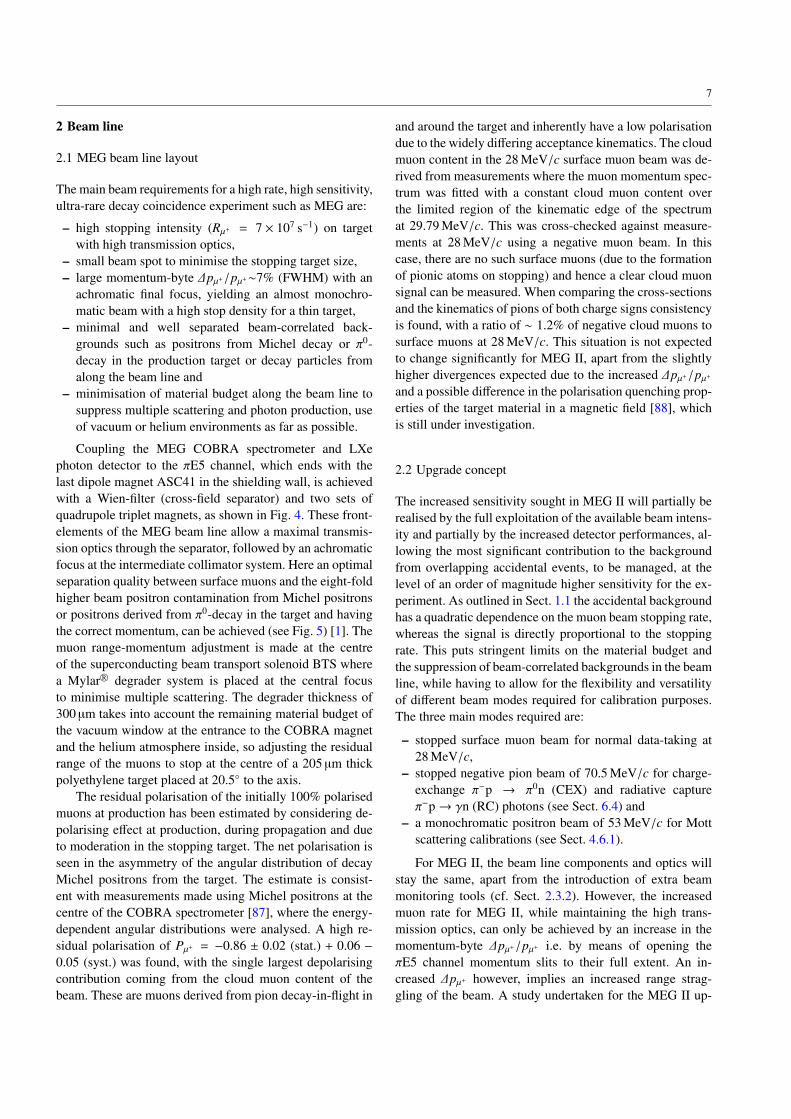
Figure 27 CDCH end-plate scheme.
Pre-amplified differential signals are successively digit-ised by the WaveDREAM board at a (programmable) speedof 2 GSPS (Giga-samples per second) with an analoguebandwidth of 1 GHz [100].
The current consumption for each channel is 60 mA ata voltage supply of ±2.5 V; this correspond to a total powerdissipation per end-plate of about 300 W, therefore an ap-propriate cooling system relying both on recirculation ofcoolant fluid and on forced air is foreseen.
4.4 The wiring procedure
A wiring system robot [102] has been designed and as-sembled in the clean room (see Fig. 28). It allows to auto-matically stretch the wires on PCB frames, keeping undercontrol the wire tension and pitch parameters; moreover thesystem fixes the wires on the PCB by a contact-less solder-ing. Since CDCH has a high wire density (12 wires/cm2),the classical feed-through technique, as a wire anchoringsystem, is hard to implement, therefore the development ofa new wiring strategy was required.
The wiring robot has been designed with the followinggoals:
- managing a very large number of densely spaced wires,- applying the wire mechanical tension and maintaining
it constant and uniform throughout all the winding pro-cess,
- monitoring the wire positions and their alignmentswithin a few tens µm,
- fixing the wires on the PCB with a contact-less solderingsystem and
- monitoring the solder quality of the wires to the support-ing PCBs.
These requirements are satisfied by the following three sys-tems:
1. A wiring system that uses a semi-automatic machine tosimultaneously stretch the multi-wire layer with a highdegree of control on the wire mechanical tension (bet-ter than 0.2 g) and on the wire position (of the order of20 µm) .
2. A soldering system composed of an infrared (IR) lasersoldering system and tin-feeder.
3. An automatic handling system which extracts themulti-wire layers from the wiring system and placesthem in a storage/transport frame.
A dedicated LabView R© software [102], based on a Com-pactRIO platform [103], controls the three systems simul-taneously, sequencing and synchronising all the different op-erations.
4.4.1 Wiring system
The purpose of the wiring system is the winding of a multi-wire layer consisting of 32 parallel wires at any stereo angle.In order to achieve a multi-wire layer (see Fig. 29), twoPCBs, aligned and oriented at the proper stereo angle, areplaced back-to-back on the winding cylinder. The multi-wirelayer is obtained in a single operation by winding along ahelical path the same wire 32 times around the cylinder witha pitch corresponding to the wire PCBs spacing. The correctpitch is achieved by a system of synchronised stepping mo-tors, through the CompactRIO system and controlled by adigital camera with position accuracy of the order of 20 µm.The wire mechanical tension is monitored by a high preci-sion strain gauge and corrected with a real-time feedbacksystem acting on the wire spool electromagnetic brake.
The wire tension variations are of the order of ±1.5 g,without the feedback system, because of the mechanical tol-erances. The feedback system reduces these variations toabout ±0.2 g (see Fig. 30).
4.4.2 Soldering system
The soldering phase is accomplished by an IR laser sol-dering system (LASCON Hybrid with a solder wire feeder[104]). Each wire is fixed at both ends while still constrainedaround the winding cylinder under its own tension. The lasersystem is controlled by the CompactRIO and it is synchron-ised with the positioning system by using a pattern match-ing software to localise the soldering pad. All the solderingparameters (temperature, soldering time, solder wire lengthand feeding speed) are defined through a proper script.

20
Figure 28 The wiring robot.
Figure 29 A multi-wire frame.
4.4.3 Automatic handling system
The wound layer of soldered wires around the cylinder isunrolled and detensioned for storage and transport. This isaccomplished with an automatic device. The first wire PCBis lifted off from the cylinder surface with a linear actu-ator connected to a set of vacuum operated suction cups andplaced on the storage and transport frame. The unrolling isaccomplished by synchronising the cylinder rotation withthe linear displacement of the frame. Once the layer ofsoldered wires is completely unrolled, the second wire PCBis lifted off from the cylinder, as the first one, and placed onthe frame. The frame hosts two supports made of polycar-bonate, dedicated to holding the wire PCBs at the correctposition by means of nylon screws. One of the two supportscan slide into the frame by adjusting the wire length, witha longitudinal threaded rod. The wiring information relativeto each frame is stored in a database. Then the wires on theframe are examined, stored and prepared for transportationto the CDCH assembly station.
Figure 30 Top: the distribution of the wire tension during the winding.Bottom: average wire tension for each loop.
4.5 The assembling procedure
The assembly of the drift chamber is as critical as the wiringphase and has to be performed under very carefully con-

21
trolled conditions [105]. In fact, to reach the required ac-curacy on the drift chamber geometry and to avoid over-tensioning of wires, it is necessary to measure the position ofthe end-plates to better than 100 µm. For example, an errorof 1 on the twist angle can correspond to an extra elonga-tion of the wire of about 1 mm. It is therefore very importantto have accurate position measurements over the chamberlength of ∼2 m. For this reason, the assembly is performedby using a coordinate measuring machine; the machine, aDEA Ghibli [106], has a maximum machine travel distanceof 2500 mm × 1500 mm × 1000 mm and a nominal accuracyof 5 µm with a contact measuring tool. The measurements ofthe positions of the PCBs are performed using an optical toolfor the identification of the cross marks placed on the PCBs.The accuracy of the optical measurement is ∼20 µm in thehorizontal plane and (making use of the focal distance of theoptics) ∼40 µm on the vertical axis.
The first test on the wire trays is a quick measurement ofthe elongation-tension curve in the proximity of the work-ing point. In this test the wire elongation is measured withthe optical tool of the measuring machine and the wire ten-sion is measured both by acoustic and electrical methods. Inthe acoustic method a periodic signal at a frequency closeto the wire resonance is measured in the readout circuit byapplying a HV difference between two adjacent wires andby using an acoustic source to excite the wires’ oscillation.This system has the ability of measuring simultaneously upto 16 wires. In the electrical method the wire oscillation isforced by applying a HV signal at a known frequency. Themutual capacitance variation between two adjacent wires isthen measured during a HV frequency scan on an externalauto oscillating circuit connected to the wires.
The drift chamber assembly is performed in safe con-ditions with unstretched wires: the distance between theend-plates is fixed at 1906 mm, 6 mm less than the nominallength (1912 mm) and 2 mm less than the untensioned wirelength. The positioning of the wire trays on the drift cham-ber is done in a well-constrained way using a rocker arm,shown in Fig. 31.
The wire tray is first engaged to the rocker arm by meansof two precision pins fitting two PCB holes and a clip. Therocker arm is then engaged to a support that leaves it free torotate and transfers the wire tray on the end-plates betweentwo spokes. The final positioning is driven by hand thoughdedicated nippers. The wire PCBs are glued on the PEEKspacers with double sided tape previously applied on the in-ner layer. The PEEK spacers are needed to separate the lay-ers at the right distance. Two pressing arches are used forensuring a good adhesion of the tape.
In Fig. 32 and Fig. 33 we show two pictures of the driftchamber after the completion of the two internal guard wirelayers. In Fig. 32 the crossing of the layers in the two stereo
Figure 31 Pictures of the rocker arm during the tray-mounting pro-cedure.
Figure 32 An end-plate after mounting about the 80% of the wires.
views is visible, while Fig. 33 shows the hyperbolic profileof the drift chamber.

22
Figure 33 The entire drift chamber with all layers mounted. The hyperbolic profile of the chamber is visible.
4.6 Calibration and monitoring
Michel events represent the natural way to continuouslyand fully characterise the spectrometer with dedicated pre-scaled triggers. The Michel positrons at the edge of the con-tinuous energy spectrum are actually used to perform thealignment of the spectrometer, to define the energy scale ofthe detector and to extract all the positron kinematic variableresolutions (energy, time and angular variable resolutions).
4.6.1 The Mott monochromatic positron beam
The continuous Michel positron spectrum makes the calib-ration difficult and subject to significant systematic errors,while delivering mono-energetic positrons would bring im-portant advantages.
Positrons are an abundant component of theMEG/MEG II beam (eight times more intense thanthe µ+-surface component, but they are normally separatedand rejected). Turning the muon beam into a positronbeam line and tuning the positron momentum very closeto the µ+ → e+γ signal energy (pe+∼53 MeV/c), a quasi-monochromatic intense beam (σbeam
pe+∼250 keV/c, Ie+
∼107 e+/s) can be Mott scattered on the light nuclei presentin the muon stopping target, providing a very useful e+-linefor a full understanding of the spectrometer from alignmentto the positron kinematic variables’ resolution.
The merits of the method, some of them unique, can belisted as
– Spectrometer absolute energy scale determination.– Spectrometer alignment: the alignment is performed as
an iterative procedure on the residuals of the expectedand measured hits of the tracks. The alignment is ex-ecuted with the detector under normal running condi-tions (i.e. with the magnetic field on) using curved trackshaving monochromatic energy which simplify the pro-cedure.
– Spectrometer checks: the well known relative depend-ence of the Mott scattered positron-momentum on theangular variables φe+ and θe+ makes possible a detailedinvestigation of the spectrometer, any distortion wouldsignal deviation from the expected detector behaviour.
– Spectrometer acceptance: the well known Mott crosssection permits the direct measurement of the spectro-meter acceptance.
– Independent check of the muon polarisation: the com-parison of the Michel versus Mott θe+ -distribution, aftertaking into account the θ cross-section dependence of theMott events, allows a cross-check of the muon polarisa-tion at the Mott positron energy.
– Positron momentum and angular resolutions: positronmomentum and angular resolutions are extracted us-ing double-turn track events. The double-turn track is

23
[MeV]+eE
40 42 44 46 48 50 52 54 56 58 60
Cou
nts
[a.u
.]
0
0.02
0.04
0.06
0.08
0.1
0.12
Figure 34 The Mott scattered positron energy distribution in ourspectrometer angular acceptance with a mean value at at Ee+ =
(51.840 ± 0.003) MeV. The comparison between data (black dotpoints) and MC simulation (red dashed area) is shown.
divided in two independent tracks, the two tracks arepropagated towards the target and the difference betweenthe relevant observable (i.e. the pe+ , φe+ or θe+ variable)is computed.
As final remarks it should be noted that the high Mott po-sitron rate enables for a fast calibration, the method does notrequire a dedicated target (i.e. the Mott target is the MEG IImuon stopping target) and does not need additional beaminfrastructures.
The potential of this method has been proven using ded-icated beam tests performed at the πE5 beam line (i.e. theMEG II beam line) with the MEG spectrometer in 2012.Figure 34 shows the good agreement between the Mott e+-line (black dot points) and the Monte Carlo (MC) simula-tion prediction (red dashed area). The data are fitted witha double Gaussian function: one taking into account thecore of the distribution and one the low energy tail. Withthe beam momentum slits virtually “fully closed” we get aline centred at Ee+ = (51.840 ± 0.003) MeV with a widthσcore
Ee+= (412 ± 10) keV.
The ability of performing the spectrometer alignmentand obtaining consistent results can be seen in Table 2 whichshows a reconstructed set of Mott data taken in 2013 basedon the Michel alignment versus Mott alignment: both themean energy and width are compared. The two data sets arein good agreement. The two different methods allow differ-ent systematic errors to be identified.
Similarly a comparison between the pe+ and angularvariable resolutions extracted using the double-turn trackmethod applied to the Mott sample and the Michel samplehas also been performed. An example of the θe+ -angular dis-
hdelta_thetaEntries 13188Mean 0.001619Std Dev 0.01711
/ ndf 2χ 44.88 / 53p0 0.0000702± 0.0008218 p1 0.000293± 0.009185 p2 0.00122± 0.02118 p3 0.0323± 0.8362
[rad]θ∆0.15− 0.1− 0.05− 0 0.05 0.1 0.15
Eve
nts
0
200
400
600
800
1000
1200
hdelta_thetaEntries 13188Mean 0.001619Std Dev 0.01711
/ ndf 2χ 44.88 / 53p0 0.0000702± 0.0008218 p1 0.000293± 0.009185 p2 0.00122± 0.02118 p3 0.0323± 0.8362
Entries 13188
/ ndf 2χ 44.88 / 53
coreµ 0.0000702± 0.0008218
coreσ 0.000293± 0.009185
tail
σ 0.00122± 0.02118
coref 0.0323± 0.8362
Figure 35 The distribution of ∆θ = θ1 − θ2 as obtained using the Mottdata sample and the double-turn method, where θ1 and θ2 are the recon-structed θ-angles associated with the first and second part a double-turntrack, respectively. The distribution is fitted with a double Gaussianfunction.
tribution obtained using the Mott sample and applying thedouble-turn method is shown in Fig. 35. Actually the doubleturn resolutions on all positron variables measured with theMott sample were found to be similar or even better (up to20%) than that measured in the Michel data. The differencehas been understood in terms of the different pile-up condi-tions in which the spectrometer works in the two cases. Thisis another example in which independent methods comple-ment each other for a better understanding of the detector.
Figure 36 shows how the method is very sensitive to mis-alignment. The red points show the expected dependence ofthe reconstructed Ee+ versus the reconstructed φe+ ; the greenpoints show the same measurement in presence of an erro-neous set of survey data used as input to the alignment pro-cedure; the plot highlights unambiguously the problem. It isalso possible to reproduce the plot in the simulation whenusing inconsistent alignment data (see the yellow points).
These results validate the method as a standard calibra-tion tool for MEG II.
4.7 Expected performances
As preliminary tests, the spatial resolution and the ageingproperties of the chamber have been measured on proto-types.
For a precise measurement of the single-hit resolution,several drift chamber prototypes were tested in a cosmic rayfacility set-up [94, 107], and an example result is shown inFig. 37. Expected biases and resolution tails are observed,

24
Table 2 The Mott e+energy spectrum: comparison between reprocessed data based on Michel vs. Mott alignment for 2013 data.
Parameter Michel Alignment Mott Alignment Difference (Mott–Michel)
Number of events 80 339 79 059 −1.6%Ee+ (MeV) 51.793 ± 0.003 51.762 ± 0.003 −0.031σcore
e+ (keV) 491 ± 2 507 ± 3 16
[deg]φ40− 20− 0 20 40 60
[M
eV/c
]+
eE
49.5
50
50.5
51
51.5
52
52.5
53
53.5
Figure 36 Reconstructed Mott positron energy versus reconstructed φ-angle. Under normal functioning conditions the trend of energy versusthe φ-angle is flat (red points). If some distortions are present, devi-ations are observed, as shown in the case of green and yellow points.See the text for more details.
h_py__1Entries 20411Mean 0.04528Std Dev 0.1986
x-b (mm)0 0.5 1
mµev
ents
/ 20
0
200
400
600
800
1000
1200 h_py__1Entries 20411Mean 0.04528Std Dev 0.1986
/ ndf 127.7 / 312χ 13 ±A 1099
0.002 ± -0.0155 µ 0.002 ± 0.106 σ 0.003 ± 0.078 δ
Integrated on all impact parameters
Figure 37 CDCH single hit resolution function, measured on a pro-totype in a cosmic ray facility, as the difference between the measureddrift distance x and the particle’s impact parameter b. A fit is performedwith a Gaussian core function of mean µ and width σ, analyticallymatched with an exponential tail starting at µ + δ (see [94] for moredetails).
due to the poor ionisation statistics in the very light helium-based gas mixture. Despite the presence of these tails, thebulk of the resolution function has a Gaussian shape, with awidth of σr ' 110 µm, averaged over a large range of anglesand impact parameters. Since the longitudinal coordinate of
Figure 38 Gain drop in one year of DAQ time.
Table 3 Expected MEG II CDCH performances compared with MEGDCH (core resolutions).
MEG MEG II
σcorepe+
(keV) 306 130σcoreθe+
(mrad) 9.4 5.3σcoreφe+
(mrad) 8.7 3.7Tracking efficiency (%) 65 78CDCH-pTC matching efficiency (%) 45 90
hits is determined by exploiting the stereo angle, the corres-ponding resolution is then expected to be σz = σr/ sin θs '
1 mm. However in the final chamber further improvementsare expected due to the new front-end electronics with a1 GHz bandwidth allowing for the exploitation of the clustertiming technique.
The operation and performance of the chamber will alsobe affected by the extremely high positron rate in CDCH(up to ∼30 kHz cm−2), which will induce a huge amountof charge collected in the hottest portion of the innermostwire (∼0.5 C cm−1). Since at such values of collected chargewire chambers can present inefficiencies and loss of gain,laboratory tests on prototypes in a dedicate irradiation facil-ity set-up were performed [94]. Tests returned sustainablegain losses of less than 20% per DAQ year (see Fig. 38) inthe hottest few centimetres of the innermost wires, an ef-fect which can be easily compensated for by increasing thevoltage of the affected wires.
The expected CDCH performance compared to theMEG DCH system is summarised in Table 3. The resolu-tions are obtained using the results of tests with prototypesas input for the simulation of the detector (under the assump-tion of Gaussian single hit resolutions), and cross-checkedwith a full simulation of the detector response (which alsoaccounts for non-Gaussian tails). Non-Gaussian tails are ob-

25
served in the resolution functions, as expected from Cou-lomb scattering at large angles and from energy-loss fluctu-ations. Core resolutions are shown in Table 3, but the fullresolution functions have been used for the estimate of theMEG II sensitivity.
In the table we quote separately the efficiency for track-ing a signal positron and the probability that such a posi-tron reaches the pTC in a place that can be geometricallymatched to the reconstructed track (matching efficiency).In MEG, the matching efficiency was limited by the posi-tron scattering on service materials (electronics, cables, etc.)in the volume between the drift chambers and the timingcounter. The new design significantly reduces this loss ofefficiency, and the estimated transparency toward the pTC isdoubled. The preliminary estimate of the tracking efficiencyin MEG II is expected to improve with further developmentsof the reconstruction algorithms.

26
5 Pixelated timing counter
Precise measurement of the time coincidence of e+γ pairs isone of the important features of the MEG II experiment inorder to suppress the predominant accidental background.The positron time te+ must be precisely measured by thepixelated timing counter (pTC), succeeding the MEG timingcounter, with a resolution σte+ ∼ 30 ps at a hit rate ∼5 MHz.In addition, it also generates trigger signals by providingprompt timing and direction information on the positron.
5.1 Limitations of the MEG timing counter
In the past decades, timing detectors based on scintilla-tion counters with PMT read-out have been built and oper-ated successfully. The best achievements with this techniquegave time resolutions slightly better than 50 ps for a min-imum ionising particle (e.g. [108,109]). One of them was theMEG timing counter consisting of 30 scintillator bars (BC-404 with 80 × 4 × 4 cm3 dimensions) each of which read outby fine mesh PMTs at both ends [110]. It showed a good in-trinsic time resolution of 40 ps in beam tests, but the operat-ive time resolution on the experimental floor was measuredto be σte+∼70 ps. The main causes of the degradation were:
1. a large variation of the optical photon paths originat-ing from the large size of the scintillator (long longit-udinal propagation and incident-angle dependence dueto its thickness),
2. a degradation of the PMT performance in the MEG mag-netic field,
3. the error of timing alignment among the bars (time cal-ibration) and
4. the electronic time jitter.
The sum of all these contributions accounted for the abovementioned operating timing resolution.
Furthermore, a positron crossing a bar sometimes im-pinged on the same bar again while moving along its approx-imately helical trajectory. Such double-hit events produceda tail component in the timing response function.
Finally, since the PMTs worked at the far edge of itsperformance versus single event rate (1 MHz per PMT), thedesigned increase of the muon stopping would have requireda segmentation of at least the same factor with respect to thepresent configuration in order to preserve the proper PMTworking point.
5.2 Upgrade concept
We plan to overcome such limitations by a detector based ona new concept: a highly segmented scintillation counter. Inthe new configuration, the 30 scintillator bars are replaced
by 512 small scintillation tiles; we call the new detectorpixelated timing counter (pTC). There are several advant-ages in this design over the previous one:
1. The single counter can easily have a good time resolu-tion due to the small dimensions.
2. The hit rate of each counter is under control to keep thepile-up probability as well as the ‘double-hit’ probabilitynegligibly low.
3. Each particle’s time is measured with many counters tosignificantly improve the total time resolution.
4. A flexible detector layout is possible to maximise thedetection efficiency and the hit multiplicity.
The third point is of particular importance: by properly com-bining the times measured by Nhit counters, the total timeresolution is expected to improve as
σte+ (Nhit) =σ
singlete+
√Nhit
=σcounter
te+⊕ σinter-counter
te+⊕ σelec
te+
√Nhit
, (7)
where σsinglete+
is the total time resolution of a single-countermeasurement which includes the counter intrinsic resolu-tion σcounter
te+, the error in time alignment over the counters
σinter-counterte+
and the electronics jitter σelecte+
. The contributionof the multiple Coulomb scattering, which does not scalelinearly with
√Nhit, is negligible. Therefore, the multi-hit-
measurement approach overcomes most of the limitationsmentioned above and is superior to pursuing the ultimatetime resolution of a single device. Note that to properly com-bine the hit times, the positron propagation times betweenthe counters have to be well known; the trajectory extrapol-ated from CDCH is used as well as refinement of it by thereconstructed counter hit positions.
This pixelated design became possible by using a newtype of solid state photo-sensor: the silicon photomultiplier(SiPM), that is a valuable replacement of the conventionalPMT because of its excellent properties as listed below:
– compact size,– sensitivity to single photons,– high internal gain (105–106),– high photon detection efficiency peaked at λ∼450 nm,– good time resolution (<100 ps for a single photon),– immunity to magnetic fields,– low bias voltage (<100 V) and low power consumption,– no avalanche fluctuation (excess noise factor 1–1.5) and– low cost.
The compactness and low cost of SiPMs allows a high seg-mentation and together with the high immunity to magneticfields enables flexible design of the counter layout withoutdeterioration of the performance in the COBRA field. Ahigh time resolution of a SiPM-based scintillation counterwas demonstrated in [111] prior to designing MEG II. Itshould also be the best solution for the read-out of the pixelmodule in this detector.

27
Figure 39 Design of the downstream pTC super-module.
5.3 Design
The pTC consists of two semi-cylindrical super-moduleslike the previous ones, mirror symmetric to each other andplaced upstream and downstream in the COBRA spectro-meter. Figure 39 shows one of the super-modules composedof 256 counters fitted to the space between the CDCH andthe COBRA magnet. The volume is separated from theCDCH, with the pTC modules placed in air.
Each counter is a small ultra-fast scintillator tile withSiPM read-out described in detail in Sect. 5.3.1. Sixteencounters align in the longitudinal (z) direction at a 5.5 cminterval, and 16 lines are cylindrically arranged at a 10.3
interval, alternately staggered by a half counter. The coun-ters are tilted at 45 to be approximately perpendicular to thesignal e+ trajectories. The total longitudinal and φ coveragesare 23.0 < |z| < 116.7 cm and −165.8 < φ < 5.2, respect-ively, which fully cover the angular acceptance of the e+
from µ+ → e+γ decays when the photon points to the LXephoton detector. This counter configuration was determinedvia a MC study to maximise the experimental sensitivity(given by the detection efficiency and the total time resolu-tion) within the constraint of a limited number of electronicsread-out channels (1024 channels in total).
5.3.1 Counter module design
The single counter is composed of a scintillator tile andmultiple SiPMs. The counter dimensions are defined by thelength (L), width (W), and thickness (T ) of the scintillatortile and described as L ×W × T below. Multiple SiPMs areoptically coupled to each W × T side of the scintillator. Thesignals from the SiPMs on each end are summed up and fed
to one readout channel. The e+ impact time at each counteris obtained by averaging the times measured at both ends.
We performed an extensive study to optimise the singlecounter design, starting from a comparative study of scintil-lator material, SiPM models, number of SiPMs per counter,and connection scheme. Then, an optimisation of the scin-tillator geometry was performed to find the best comprom-ise between the total resolution, detection efficiency and re-quired number of channels. The results are reported in detailin [112–115] and summarised below.
5.3.1.1 Scintillator The choice of the scintillator material iscrucial to optimise the time resolution. The candidates se-lected from the viewpoint of light yield, rise- and decay-times, and emission spectrum are the ultra-fast plastic scin-tillators from Saint-Gobain listed in Table 4. Note that thesmaller counter dimensions allow the use of such very shortrise time scintillators, which typically have short attenuationlengths. The time resolutions were measured for all the typesof scintillator and different sizes. BC-422 was found to al-ways give the highest time resolution for each size (testedup to 120 × 40 × 5 mm3) and therefore was chosen.
Different type of reflectors such as no reflector, Teflon R©
tape, aluminised Mylar R© and enhanced specular reflector(ESR) from 3M were tested to improve the light collectionand hence the time resolution. The best time resolution wasobtained with ESR film, while a small worsening was ob-served with Teflon tape (diffuse reflector) compared to noreflector [112].
5.3.1.2 SiPM The photo-sensors must be sensitive to thescintillation light in the near-ultraviolet (NUV) range. Re-cently, several manufacturers have developed such NUV-sensitive SiPMs based on ‘p-on-n’ diode structures. There-fore, we tested a number of such NUV-sensitive SiPMsavailable as of 2013 from AdvanSiD (ASD), HamamatsuPhotonics (HPK), KETEK, and SensL.
Before the decision of SiPM models, we first examinedthe schemes of SiPM connection. In order to compensatethe small active area of SiPMs, multiple SiPMs are con-nected in parallel for read-out. However, performance is-sues for the parallel connection are: increase in the signalrise time and width and increase in the parallel and seriesnoise; both originate from the larger sensor capacitance andnegatively affect the time resolution. We have examined analternative connection: series connection of multiple SiPMs(NSiPM = 3−6).7 Figure 40 shows a comparison of time res-olutions between series and parallel connections. Series con-nection gives better time resolutions at all over-voltages.8
7Series connection of avalanche photodiodes was proposed and testedin [118] and the first application to SiPMs is found in [119].8The over-voltage is the excess bias voltage over the SiPM breakdownvoltage. In the series connection case, it quotes over-voltage per SiPM.

28
Table 4 Properties of ultra-fast plastic scintillators from Saint-Gobain. The properties of BC-404, which was used in the previous timing counterbar, is also shown for comparison.
Properties BC-418 BC-420 BC-422 BC-422Q BC-404
Light Outputa) (% Anthracene) 67 64 55 19 68Rise Timea)b) (ns) 0.5 0.5 0.35 0.11 0.7Decay Timea) (ns) 1.4 1.5 1.6 0.7 1.8Peak Wavelengtha) (nm) 391 391 370 370 408Attenuation Lengtha) (cm) 100 110 8 8 140Time Resolutionc) (ps) 48 ± 2 51 ± 2 43 ± 2 66 ± 3 –
a)From Saint-Gobain catalogue [116].b)Those values are dominated by the measurement setup. The intrinsic values are much faster.For example, a BC-422 rise time of <20 ps was reported in [117].c)Measured value in [114] with 60 × 30 × 5 mm3 sized counter read-out with 3 HPK SiPMs(S10362-33-050C) at each end.
OverVoltage(V)1 2 3
Res
olu
tio
n(p
s)
40
60
80
100
120
Parallel
Series
Figure 40 Comparison of time resolutions between series and paral-lel connections measured with 60 × 30 × 5 mm3 sized counter read-outwith 3 HPK SiPMs (S10362-33-050C) at each end (from [115]).
This is due to the narrower output pulse shape because ofthe reduced total sensor capacitance in the series circuit. Al-though the total charge (gain) is reduced to 1/NSiPM of thatof a single SiPM, the signal amplitude (pulse height) is keptcomparable (compensated by the NSiPM times faster decaytime). Thus, we conclude that series connection is better forthe pTC application. We simply connect SiPMs in series ona custom print circuit board (PCB) while we adopt a morecomplex way for the MPPCs used in LXe photon detector(see Sect. 6.2.7).
For each type of SiPM, we measured the device char-acteristics (such as dark count rate, cross-talk probability,PDE, and temperature dependence) and the time resolutionwhen coupled to a scintillator. The main results are shownin Fig. 41. The best time resolution is obtained with SiPMsfrom HPK, which have the highest PDE. This result indic-ates that the time resolution of our counter is predominantlylimited by the photon statistics and increasing the number ofdetected photons is the most important and straightforward
Over voltage/SiPM (V)2 4 6 8
Res
olu
tio
n (
ps)
30
40
50
60
70
80
90
100S1036233050C S12572050C(X)
S12572025C(X) 3X3MM50UMLCTB
PM3350 prototypeA ASDNUV3SP50
MicroFB30050SMT
Figure 41 Time resolutions measured with different types of SiPMs(3 SiPMs at each end) and 60 × 30 × 5 mm3 scintillator (from [114]).
way of improving the time resolution. Using higher PDESiPMs is one way.
Another way is increasing the sensor coverage by us-ing more SiPMs. Figure 42 shows the time resolution meas-ured with different numbers of SiPMs. In this study, SiPMsfrom ASD were used. A clear improvement with a lar-ger number of SiPMs is observed, and a time resolutionof 50 ps is achieved with 6 SiPMs at each end coupledto 90 × 40 × 5 mm3 scintillator. This is better than thatachieved with 3 HPK SiPMs (58 ps). The question as to howmany sensors can be used depends on the final geometry ofthe detector and cost, so the decision of the SiPM model andthe number was made after fixing those parameters. We fi-nally adopted the 6-series solution using ASD SiPMs, whichgives the best performance within our budget constraint.
The model used in the pTC is the ASD-NUV3S-P-High-Gain; the specifications provided by AdvanSiD are listedin Table 5. Figure 43 shows the measured single-cell-firedsignal. The SiPM’s specific long exponential tail, with a

29
Over voltage/SiPM (V)3 3.5 4 4.5 5 5.5 6
Res
olu
tion
(p
s)
30
40
50
60
70
80
90
100
3Series
5Series
6Series
Figure 42 Time resolution measured with different numbers of SiPMs.3, 5, and 6 SiPMs (ASD-NUV3S-P-50) connected in series andcoupled to each end of 90 × 40 × 5 mm3 scintillator (from [115]).
Table 5 Specifications of AdvanSiD SiPM ASD-NUM3S-P-50-High-Gain.
Parameter Value Unit
Effective active area 3 × 3 mm2
Cell size 50 × 50 µm2
Cells number 3600Spectral response range 350 to 900 nmPeak sensitivity wavelength 420 nmBreakdown voltage VBD 24 ± 0.3 VWork voltage range VBD + 2 to VBD + 3.5 VDark count <100 kcps/mm2
Gain 3.3 × 10⁶
VBD temperature sensitivity 26 mV/C
Time (μs)0 0.1 0.2 0.3 0.4
Am
pli
tud
e(m
V)
0
5
10
15
20
Figure 43 Pulse shape of a single-cell-fired signal from an ASD-NUV3S-P-High-Gain (with a gain 60 amplifier). The black line showsthe averaged pulse shape and the red curve is the best fit function.
time constant of 124 ns, is due to the recharge (recovery)current determined predominantly by the quench resistanceand the cell capacitance, which are measured to be Rq =
(1100 ± 50) kΩ and CD = (100 ± 10) fF, respectively.
5.3.1.3 Geometry The single counter time resolution wasmeasured for different sized scintillator tiles, and the resultsare shown in Fig. 44. The size dependence is understandablefrom the photon statistics expected from the sensor cover-age to the scintillator cross-section (dependent on W) andthe light attenuation in the scintillator (on L).
Length (mm)60 80 100 120
Res
olu
tio
n (
ps)
30
40
50
60
70
80
50 mm wide
40 mm wide
30 mm wide
Figure 44 Dependence of the counter time resolution on the sizemeasured with 3 HPK SiPMs (S10362-33-050C) at each end. The su-perimposed curves show the dependence expected from the detectedphoton statistics. The shaded bands show the uncertainty. See [114] forthe detailed description.
The size has to be optimised by a balance betweensingle-counter resolution (smaller is better) and hit multipli-city and detection efficiency (larger is better). This optimisa-tion is performed via a MC simulation study using the meas-ured single-counter resolutions. As a result, longer counters(up to the measured maximum L = 120 mm) are found togive a better performance. Considering the hit rate and thedouble-hit probability, we did not test longer counters andfixed the length to be L = 120 mm. The optimal counterwidth W is dependent on the longitudinal position becausethe radial spread of the signal e+ trajectories depends on thelongitudinal position in the pTC region. We adopt two dif-ferent sizes: W = 40and50 mm. The W = 50 mm countersare assigned to the middle longitudinal position (see Fig. 39)where the radial spread becomes large. We observed a mod-erate dependence of the resolution on the thickness T anddecided for T = 5 mm, which is sufficiently thick to matchthe SiPM active area. A 5 mm thick scintillator causes adeflection of 50 MeV positron direction for θRMS
MS ∼25 mrad,whose impact on the propagation time estimation is estim-ated to be ∼5 ps, negligibly small compared to the counterresolution.
5.3.1.4 Final design of the counter module Figure 45 showsexamples of the final counter modules. A counter consistsof a tile of BC-422 with dimensions of L ×W × T = 120 ×(40 or 50)× 5 mm3 and 12 ASD SiPMs, 6 on each (W × T )-side, directly coupled to the scintillator with optical cement(BC-600). The scintillator is wrapped in 32 µm thick ESRfilm, and then the module is wrapped in a 25 µm thick blacksheet of Tedlar for light tightness.

30
Figure 45 Picture showing both types of counter modules. Left: W = 40 mm counter wrapped in the reflector (example with the L-shaped PCB).Right: W = 50 mm counter with optical fibre before wrapping in the reflector.
Figure 46 The SiPM mounting PCBs. The top one is for the 50 mmcounters and the others are for the 40 mm ones.
Figure 46 shows the PCBs on which the SiPMs aresoldered. The L-shaped PCBs are used for the counters at theinner (small |z|) location where the radial space is more re-stricted because of the smaller inner diameter of the magnetcoils. Parts made of aluminium are attached to the PCBs andthermally coupled to one of the metal layers on the PCBs.They are used not only to mechanically fix the counters butalso to thermally link the SiPMs to the main support struc-ture whose temperature is controlled by a chiller system.
Each counter except for the counters using the L-shapedPCBs is equipped with an optical fibre for the laser calibra-tion (described in Sect. 5.5.2).
5.3.2 Read-out chain
The basic idea of the read-out scheme is to send the rawSiPM-output signals directly to the WaveDREAM read-outboards (WDBs) (see Sect. 8), on which the signals are ampli-fied, shaped, and digitised. Hence, the SiPMs and amplifiersare separated by long cables without any pre-amplification.This approach is adopted for both simplification and forspace and power consumption reasons. The reduction ofthe sensor capacitance by the series connection allows 50 Ω
transmission without significant broadening of the pulse.
The counter modules are mounted on 1 m long cus-tom PCBs (back-planes) placed on the mechanical supportstructures, allowing the signals to be transmitted outsidethe spectrometer. The back-planes have coaxial-like sig-nal lines with a 50 Ω characteristic impedance. The groundlines are independent of each other to avoid possible groundloops. The signals are then transmitted to the WDBs on7 m long non-magnetic RG-178 type coaxial cables (Radi-all C291 140 087). MCX connectors are used for all connec-tions.
The SiPM bias voltages, typically 164 V for the six ASDSiPMs in series, are supplied from the WDBs through thesignal lines; only one cable per channel.
The input signals are amplified by a factor 100 at theanalogue part of WDBs. It turns out to be very importantto eliminate the long time constant component of the SiPMoutput pulse for a precise time measurement in order to sup-press the effect of dark counts and obtain a stable baseline,especially after some radiation damage. For this reason apole-zero cancellation circuit is incorporated on the WDB.
The amplified and shaped waveforms are digitised at asampling frequency of 2 GSPS by the DRS4 chips on theWDBs for a detailed offline analysis of the pulses in orderto compute the precise signal times.
5.3.3 Mechanical support structure
The mechanical support structures are made of aluminiumcylinders with inner and outer radii of 380 mm and 398 mm,respectively. The back-planes are fit to grooves machinedon the structures. A hole is drilled below the centre of eachcounter to pass an optical fibre from underneath. Cooling-water pipes are laid on the outer side of the structure andconnected to the chiller to keep the temperature below 30 Cwith a stability better than 1 C.9
9The main heat source is the front-end electronics of CDCH (Sect. 4.3).

31
5.4 Hit distribution & rate
A MC simulation based on Geant4 (version 10.0) [120–122]is performed with the final detector configuration to evalu-ate the hit distribution and hit rates. Figure 47 shows an ex-ample of a hit pattern in the pTC by a e+from a µ+ → e+γ
decay. Figure 48 shows the distribution of the number ofhit counters for signal positrons generated in the angularacceptance.10 The mean hit multiplicity is evaluated to beNhit = 9.3.
The hit rates at the individual counters are estimated by asimulation of a µ+-beam (at a rate 9 × 10⁷ s−1)11 which thendecay in accordance with the SM calculation. The result isshown in Fig. 49 as a function of z-position of the coun-ters. The rates are position dependent, and the maximum is160 kHz. This result is confirmed by measurements in thepilot run described in Sect. 5.6.
5.5 Calibration methods
It is also quite important to precisely synchronise all thecounters, although the effect of the misalignment of the in-dividual counter times can be diluted by taking the averageover the multiple hit counters as seen from Eq. (7). Con-sidering the dilution effect, σinter-counter
te+∼30 ps is required for
the precision of each counter time-alignment. Two schemesare under development for the inter-counter time-alignment.They are complementary to each other and have independentsystematic errors.
5.5.1 Track-based method
High momentum Michel positron pass through more thanone counter as would signal one. Multiple hits allow time-alignment between adjacent counters after correcting for thee+ travel time between hits. The track information analysedby the CDCH can be used for a precise correction of thetravel time. Generally, the track-based method provides veryprecise results; O(ps) is achieved in a study using a MCsimulation. However, this method is subject to systematicposition-dependent biases caused by small systematic er-rors in the travel time estimation. Such biases will be de-tected and corrected for by the laser-based method detailedin Sect. 5.5.2. Furthermore, this method cannot be used tosynchronise the two super-modules.
10Defined so that the corresponding photon (with a direction oppositeto the e+) enters the fiducial volume of the LXe photon detector.11It is necessary because Michel positrons from off-target decays (es-pecially downstream of the target) have a non-negligible effect on therates.
5.5.2 Laser-based method
The counters can also be time-aligned by distributing syn-chronous light pulse to all the counters through opticalfibres. To this goal, we have developed a laser calibrationsystem shown schematically in Fig. 50 (see also [124]).Ideally we should distributing lase light to all counters, how-ever, it turned out to be impossible to install optical fibres tothose at the innermost location (in total 80 counters) due tospace limitation. For those counters, we rely on the calibra-tion by the track-based method detailed in Sect. 5.5.1.
The light source is a PLP10-040 [125], with an emissionwavelength at 401 nm, pulse width of 60 ps (FWHM) andpeak power of 200 mW. The fast light pulse is first split intotwo outputs; one is directed to a photodiode to gauge thesignal amplitude, and the other serves as an input to an act-ive optical multiplexer [126] with nine output channels andremotely controlled, such that the signal is outputted altern-atively to each of them.
Each of the outputs of the multiplexer (except one usedas a monitor) is then inputted to two cascaded stages of 1 × 8optical splitters [127]. each of which splits the input signalinto eight signals of approximately equal output amplitudes.As a result, 64 channels become available in parallel withan amplitude ∼1/64 of the original (actually smaller due tolosses in the various stages). Finally, each output signal fromthe last stage of splitters is fed into a counter through anoptical fibre. Figure 51 shows how the optical fibre is fixedto the scintillator: to stably fix the fibre, a small hole (2.5 mmdiameter, 1 mm depth) is drilled into the bottom face of thescintillator, and the ferrule of the fibre is inserted into thehole using a polycarbonate screw and a support bar (ABSresin) across the two PCBs.
As mentioned in Sect. 5.6, we performed pilot runs us-ing the MEG II beam. In the 2016 run, we installed the lasercalibration system for 40 counters and tested the system byexamining the consistency with the track-based time calibra-tion method detailed in Sect. 5.5.1. The time offset of eachcounter was calculated independently using two methods.Figure 52 shows the difference between the results of thetwo methods. The dispersion (39 ps in standard deviation)includes the systematic errors of both methods, therefore,the precision of each method is better. The time dependencewas stable during the 3-week-run to a σ = 6 ps. By combin-ing the two methods, it is possible to calibrate all the counteroffsets to a precision better than σinter-counter
te+= 30 ps. The
average contribution to the inter-counter calibration can beevaluated as σinter-counter
te+/√
Nhit = 10 ps.
5.6 Expected performance
The single-counter performance is evaluated using electronsfrom a 90Sr source. All the assembled counters were irradi-

32
Side view
View from downstream
Figure 47 An example of a hit pattern by a simulated signal e+. CDCH is not drawn in these figures.
Mean 9.281
0 5 10 15 20
Nhit
Fre
qu
ency
(a.u
.)
0
0.5
1
Figure 48 Distribution of the expected number of hit counters for sig-nal positrons, from a MC simulation.
ated by the electrons at three positions (−45, 0 and 45 mmalong L) to measure the time resolution, position resolution,light yield, and effective light speed veff . The pulse timeof each read-out side is picked-off by the digital-constant-fraction method (t1 and t2). The hit time is then reconstruc-ted by averaging the two times, (t1 + t2)/2, while the hitposition along L is reconstructed by the time difference,(t1 − t2) × veff/2. The mean time resolutions for all as-sembled counters are 72 ps and 81 ps for W =40 mm and50 mm counters, respectively. These are about 15% worsethan those obtained with the prototype counters in the R&Dphase because of the quality control of SiPMs and scintillat-
Counter position ID0 5 10 15 20 25 30
Hit
rate
(k
Hz)
0
50
100
150
Data
MC
40 60 80 100z (cm)
Figure 49 Counter hit rate under MEG II beam conditions, as a func-tion of counter z-position. The black squares are from the MC simula-tion and the red circles are from the pilot run. The points with zero hitrate are due to dead channels in the readout electronics (from [123]).
ors in the mass production phase. The hit position resolutionis σL∼10 mm.
The performance with multiple counters was studied ina series of beam tests carried out at the Beam Test Facility(BTF) at LNF and the πE5 beam channel at PSI. Six to tenprototype counters aligned as a telescope were irradiated by50 MeV monochromatic positrons at the BTF or by Michelpositrons at PSI. The effects of multiple Coulomb scatteringand secondary particles, such as δ-rays, were examined, andthe time resolutions was found to improve by use of mul-

33
Laser head
Laser controller
1×9
1×8
1×8
1×2
Photodiode
SY
NC
sig
nal
Counter module
Mode scrambler
Photo
dio
de s
ignal
Counter signal
Optical fibre
Optical switch
Optical splitter
DAQ electronics
Figure 50 Schematic of the pTC laser calibration system.
2.5 mm
7 mm
1.5 mm
1.9 mm
1.0 mm
fibre end(Ceramic, 1.8 mm)
0.9mm
Screw
Fibre
Scintillator
Figure 51 Schematic of the fibre fixing method.
tiple counters following closely Eq. (7). Detailed reports areavailable in [115, 128].
Finally, we performed pilot runs in 2015 and 2016 usingthe MEG II µ+ beam and the one-forth system of the pTC(consisting of 128 counters) installed in the COBRA spec-trometer. The system was thoroughly tested from the hard-ware point of view: the geometrical consistency, the installa-tion procedure, and the operation under beam. The laser cal-ibration system was partially implemented and also tested.Data from Michel positrons were also taken with a prototypeof the WDBs, under various trigger conditions.
The multi-counter time resolutions are evaluated by an‘odd − even’ analysis. For a given set of hit counters, hitsare alternately grouped into ‘odd’ (Nodd) and ‘even’ (Neven)by the order of the pixels traversed by the positron, the timedifference being defined as (Nhit = Neven + Nodd)
todd−even(Nhit) =1
Nhit
Nodd∑i=1
thit(2i−1) −
Neven∑i=1
thit(2i)
.The standard deviation of todd−even(Nhit) is used as an es-timator of the time resolution for Nhit hits and examined
Laser Counter ID0 5 10 15 20 25 30 35 40
[ps]
200−
150−
100−
50−
0
50
100
150
200
Toffset(MC-LC)
Figure 52 Difference of time offsets between the laser-based methodand the track-based method at the beginning of the pilot run in 2016.The difference was calculated only for the laser-installed-counters. Thestandard deviation is 39 ps. Each error bar includes systematic uncer-tainties of the two methods.
hitN
2 4 6 8 10
Res
olu
tion
(p
s)
20
40
60
80
100
/ ndf 2χ 8.537 / 3
single 0.6224± 92.62
const 3.032± 0
/ ndf 2χ 8.537 / 3
single 0.6224± 92.62
const 3.032± 0
Figure 53 The total time resolution vs. the number of hits measuredby the ‘odd − even’ analysis in the pilot run 2016. The points are theaverage of the 22 counter-sets weighted by the event fraction. The redcurve is the best fit function of σte+ (Nhit) = σ
singlete+
/√
Nhit ⊕ σconstte+
.
for 22 sets of counters. Figure 53 shows the result ob-tained in the pilot run 2016. The total time resolution im-proves as Eq. (7) with σsingle
te+=93 ps. At the mean Nhit = 9,
σte+ (Nhit = 9)=31 ps was achieved.
5.7 Other issues
The modest radiation hardness of SiPMs is considered asa weak point of SiPMs. Increase of the dark current andchange of the gain of SiPMs are typical effects after sub-stantial irradiation. The SiPMs in the pTC will be irradiatedby a high flux of Michel positrons during the experiment.

34
Figure 54 Results from the irradiation tests of HPK SiPM (S10362-33-050C) performed by the PSI µSR group. Significant increase ofdark current (top) and 15% gain decrease (middle) are observed,while the timing resolution is unchanged (bottom). Courtesy from Dr.A. Stoykov of Paul Scherrer Institut.
The integrated fluence of the Michel positrons during three-years running is estimated to be ∼1011 e+/cm2.12
The PSI µSR group performed irradiation tests usingMichel positrons as shown in Fig. 54 [129]. The SiPMsfrom HPK are irradiated by Michel positrons with fluencesup to 2.5 × 1011 cm−2, which is more than twice higher thanMEG II expectation. They observed a significant increase ofthe dark current by a factor of six and a 15% gain decrease.Interestingly the timing resolution is unchanged even withthe highest fluence.
During the pilot run, we observed increases in the SiPMcurrent. By extrapolating the observed increase, the darkcurrent of each channel would reach O(100 µA) in the threeyears run. This is higher than the expectation from the studyabove. Further studies are necessary to assess the impact ofthe radiation damage on the timing performance. We plan tocarry out irradiation tests of our SiPMs and counter modulesusing high intensity β sources and test beams such as BTFat LNF.
The SiPMs are also irradiated by neutrons and γ-raysin our experiment. The effect is discussed in detail inSect. 6.2.2 for the SiPMs planned to be used for the LXephoton detector and it turns out not to influence the perform-ance of SiPMs.
12This estimation is based on the measured hit rate in the pilot run. Itis twenty times higher than the previous estimation in [86].
Another possible issue is the temperature stability ofthe SiPMs. The temperature coefficient of the breakdownvoltage for ASD-NUM3S-P-50-High-Gain is 26 mV C−1;the gain at an over-voltage of 2.5 V changes by 1% for atemperature change of 1 C. The temperature will be con-trolled and stabilised to within 1 C by an air-conditioningsystem of our detector hut and the cooling water system onthe mechanical support structure. Therefore, the temperat-ure dependence of the SiPMs should not be an issue in ourcase.

35
6 LXe photon detector
6.1 Upgrade concept
The liquid xenon (LXe) photon detector is a key ingredientto identifying the signal and suppressing the background inthe µ+ → e+γ search. It is, therefore, crucial to substantiallyimprove its performance in MEG II.
The MEG LXe photon detector, shown in Fig 55, wasone of the world’s largest detectors based on LXe scintil-lation light with 900 l of LXe surrounded by 846 PMTssubmerged in liquid to detect the scintillation light in theVUV range (λ = (175 ± 5) nm). The 2-inch PMT (Hama-matsu R9869) used in the detector is UV-sensitive with aphoto-cathode of K-Cs-Sb and a synthetic quartz window.The quantum efficiency (QE) was about 16% for the LXescintillation light at a LXe temperature of 165 K.
The photon entrance inner face was covered by 216PMTs with a minimum spacing between adjacent PMTs.The photo-cathode of the PMT was, however, round-shapedwith a diameter of 46 mm which was much smaller than theinterval between adjacent PMTs of 62 mm. The perform-ance of the MEG LXe photon detector was limited due tothis non-uniform PMT coverage. Figure 56 shows the effi-ciency of scintillation light collection as a function of thedepth of the first interaction for signal photons of 52.8 MeV.The collection efficiency strongly depended on the incidentposition. The non-uniform response was partly corrected forin the offline analysis, but it still deteriorated the energy andposition resolutions due to event-by-event fluctuations of theshower shape, especially for shallow events.
The main concept of the upgrade of the LXe photon de-tector for MEG II is to reduce this non-uniform response byreplacing the PMTs on the inner face with smaller photo-sensors. Figure 57 shows a comparison of how the sameevent would look for the two cases with the current PMTsand smaller photo-sensors (12 × 12 mm2) on the inner face.The imaging power is greatly improved with smaller photo-
Figure 55 MEG LXe photon detector with 900 l LXe surrounded by846 UV-sensitive PMTs.
Figure 56 Efficiency of the scintillation light collection estimated bya MC simulation as a function of the depth of the first interaction of asignal photon of 52.8 MeV.
sensors. For example, two local energy deposits in the sameshower are clearly separated in this event. It turns out thatboth the energy and position resolutions greatly improve es-pecially for shallow events as shown in Sect. 6.6.SiPMs are adopted as smaller photo-sensors for the innerface of the MEG II LXe photon detector. The motivation forchoosing SiPM is discussed in detail in Sect. 6.2.The PMTs which were used on the inner face of the MEGLXe photon detector are re-used on the other faces. It turnsout by detailed MC studies that the best use of those PMTsis achieved by modifying the layout of the PMTs on the lat-eral faces. Figure 58 illustrates the modified layout viewedon a r-z section. The inner face extends along z, outsidethe acceptance region by 10% on each side. The extendedvolume reduces the energy leakage for events near the lat-eral walls. The PMTs on the lateral faces are tilted such thatall the photo-cathodes lie in the same plane. This config-uration minimises the effect due to shower fluctuations forevents near the lateral walls. The energy resolution is thusimproved especially for those events.
6.2 Development of VUV-sensitive MPPC
6.2.1 MPPC advantage
The MPPC R© (Multi-Pixel Photon Counter), a new type ofphoton counting device produced by Hamamatsu PhotonicsK.K., is a kind of SiPM device. The MPPC has many excel-lent features suited for the MEG II experiment. It is insens-itive to magnetic fields and is sensitive to single photons,which enables an easier and more reliable calibration of thedetector. Moreover, a finer read-out granularity of the scin-tillation light with MPPCs allows for a more precise recon-

36
Figure 57 Example of scintillating light distributions detected by photo-sensors in case of (left) PMTs and (right) smaller photo-sensors(12 × 12 mm2) on the inner face for the same MC event.
Figure 58 MEG (left) and MEG II (right) layouts of the PMTs viewedin an r-z section.
struction of shallow events. Less material budget before theLXe active region results in a 9% higher detection efficiency,as discussed in Sect. 6.6. The typical bias voltage is less than100 V.
6.2.2 Issues
There are several issues to be addressed concerning the de-tection of LXe scintillation light by MPPCs.
The first issue is the photon detection efficiency (PDE)for VUV light. There are two types of layer structures forthe SiPM, p-silicon on an n-substrate (p-on-n) and n-on-p.In general, since the ionisation coefficient for electrons ishigher than that for holes, the breakdown initiation probab-ility of electrons is always higher than that of holes. Bluelight is absorbed close to the SiPM surface and electronsinitiate the avalanche breakdown in the p-on-n case, whichresults in a higher sensitivity in the blue light region. OurMPPC uses the p-on-n structure, which is suitable to detectthe blue light. The PDE of standard MPPC for VUV lightis, however, nearly zero since VUV photons can not reachthe sensitive layer due to a protection coating layer made ofepoxy resin or silicon rubber. Furthermore, an anti-reflection(AR) coating layer is not optimised to the refractive index ofLXe at the scintillation light wavelength.
The second issue is the MPPC size. The current largestsingle MPPC commercially available is 6 × 6 mm2, whichis still too small to cover the inner face of the LXe photondetector with an affordable number of read-out channels. Itis desirable to develop a large-area MPPC with 10 × 10 mm2
Figure 59 An MPPC signal waveform (upper) and a PMT signalwaveform (lower) for the same α-event digitised at a sampling fre-quency of 700 MSPS.
or larger. However, the larger size of MPPCs could cause alarger dark count rate, larger gain non-uniformity, and largercapacitance (longer tail in the waveform, larger noise etc.)[130].
A large-area UV-sensitive MPPC has been developed incollaboration with Hamamatsu Photonics to be used in theupgraded LXe photon detector. We will describe its charac-teristics in the following sections.
6.2.3 PDE
Many prototypes optimised for VUV detection have beenproduced by Hamamatsu Photonics, which have no protec-tion coating, a thinner contact layer or optimised AR coatingwith different parameters.
We succeeded in detecting the LXe scintillation lightfrom α-events by using one such prototype sample. Fig-ure 59 shows signal waveforms from the MPPC sample (up-per figure) and a UV-sensitive PMT (lower one) for the sameα event.
The number of detected photoelectrons for α-event iscalculated from the ratio of the observed charge to that ob-

37
Over Voltage (V)0 1 2 3 4 5 6 7
PD
E
0
0.05
0.1
0.15
0.2
0.25
0.3
0.35
PDE vs Over Voltage
Figure 60 Measured PDEs as a function of the over-voltage. The largeuncertainty mainly stems from the different measurement setups.
tained for a single photoelectron event. The PDE is thenestimated from a ratio of the detected number of photo-electrons to the expected number of incoming scintillationphotons from α-events. This PDE still contains contribu-tions from cross-talk, after-pulses, and the infrared com-ponent of the LXe scintillation light. The contribution fromthe infrared component is estimated to be ∼1% indirectly,by using the signal observed with a commercial MPPC(S10362-33-100C), which is supposed to be insensitive tothe VUV component. The cross-talk + after-pulse compon-ents are estimated using a flashing LED in such a way thatthe MPPC detects less than 1 p.e. on average. The expec-ted 1 p.e. probability (p1 p.e.expected) is calculated from thePoisson distribution with the mean estimated from the ob-served probability of 0 p.e. events. We can estimate thecross-talk+after-pulse probability by comparing this withthe measured probability of 1 p.e. events (p1 p.e. measured)[131]. This method yields a cross-talk + after-pulse probab-ility = (p1 p.e.expected−p1 p.e.measured)/p1 p.e.measured. of between10–50%, depending on the over-voltage.
Figure 60 shows the measured PDEs for four MPPCsamples after correcting for the contributions from cross-talk and after-pulses. There is roughly a 30% uncertaintyin the PDE value, that is estimated from the variation of thePDE measured in different setups. The result shows that thePDE is higher than the 15% PDE measured in LXe, whichis similar to the QE for the UV-sensitive PMT of the currentdetector (∼16%). Since the sensor coverage on the inner faceis increased by 50% using MPPCs, the total photoelectronstatistics would be increased.
6.2.4 Temperature dependence
Thermally generated free carriers in a depleted layer pro-duce dark counts. The typical dark count rate is 0.1–10 MHz mm−2 at room temperature. The dark count rate isknown to be suppressed by five orders of magnitude at LXe
Figure 61 The dark count rate measured at different temperatures(room temperature, 205 K and 165 K).
temperature (165 K) [132]. Our test measurements confirmthat the dark count rate is reduced down to 1.0–100 Hz for3 × 3 mm2 samples at LXe temperature as shown in Fig.61.
Poly-silicon was used in the previous versions of MPPCsas quenching resistors, but now switched to metal resistorsare more common.
However, the resistivity of the poly-silicon increaseswhen the temperature decreases, for example, the resistanceat LXe temperature is measured to be more than a factorof two higher than at room temperature. A metal quench-ing resistor, which has 1/5 of the temperature coefficient ofa poly-silicon resistor, is more suitable in our application inorder to keep the quenching resistance low, which can avoidlong fall time of MPPC signal.
The breakdown voltage of MPPCs is known to havea relatively large temperature coefficient (56 mV C−1) andthe gain and PDE can, therefore, easily shift depending onthe temperature, influencing the stability of the detector per-formances.
The LXe temperature stability of the MEG LXe photondetector has been measured to be smaller than 0.15 K(RMS), most likely dominated by the precision of the tem-perature measuring device. The fluctuation of the MPPCgain at an over voltage around 7 V is expected to be smal-ler than 0.1% (RMS). The PDE at around 7 V over voltageis already saturated, and no fluctuations are expected fromtemperature variation. The voltage dependence of the cross-talk and the after-pulse of the MPPC should be smaller than30%/V, which corresponds to 0.23%. These fluctuations aresmaller than the expected energy resolution of the MEG IILXe photon detector described in Sect. 6.6.
6.2.5 Radiation hardness
Radiation produces defects in the silicon bulk or at theSi/SiO2 interface of SiPMs. As a result, some parameters

38
of SiPMs such as the breakdown voltage, leakage current,dark count rate, gain, and PDE may change after irradiation.There have been many studies on the radiation hardness ofSiPMs irradiated by photons, neutrons, protons, or electrons.These studies show the following.
An increased dark count rate was observed at more than108 n/cm2, and loss of single p.e. detection capability wasobserved at more than 1010 n/cm2 [133]. From the neutronflux measured in the MEG experimental area, the total neut-ron fluence is estimated to be less than 1.6 × 10⁸ n/cm2 inMEG II.
Increased leakage current was observed with a photonirradiation of 200 Gy [134], while the photon dose in theMEG II is estimated to be 0.6 Gy.
The radiation damage by photons, or neutrons should notbe an issue for the MPPCs in MEG II.
6.2.6 Linearity
SiPMs show a non-linear response when the number of in-cident photons is comparable to or larger than the numberof pixels of the device. The optimal condition is that thenumber of incident photons be much smaller than the num-ber of pixels without any localisation. Figure 62 (top) showsthe measured response functions for 1 × 1 mm2 SiPMs withdifferent total numbers of pixels illuminated by a 40 pslaser pulse [135]. For the MEG II LXe detector, the expec-ted number of photoelectrons reaches up to 12 000 p.e. on12 × 12 mm2 sensor area for very shallow signal events asshown in Fig 62 (Bottom), which is only 20% of the totalnumber of pixels, 57 600. Considering also that some of thefired pixels are recovered during the emission time of thescintillation light, the expected non-linearity is, therefore,small and can be corrected for by a careful calibration.
6.2.7 Large area MPPC
The current largest MPPC (6 × 6 mm2) is still too smallfor the MEG II LXe photon detector, and we need at least10 × 10 mm2 to replace the PMTs. For a larger size sensor,we have to pay attention to a possible increase in the darkcount rate, an increase of the sensor capacitance, and gainnon-uniformity over the sensor area.
The increase of the dark count rate is not an issue inMEG II due to the LXe temperature. To reduce the sensorcapacitance, the large area of 12 × 12 mm2 is formed by con-necting in series four smaller MPPCs (6 × 6 mm2) each). Inthis configuration, the decay constant of the signal wave-form becomes 40–50 ns from 130 ns. To equalise the gain inthe large area sensor, four MPPCs are selected with similarbreakdown voltages.
Instead of a simple series connection, each sensor chipis decoupled with a capacitor to enable the bias voltage to be
Figure 62 (Top) Response functions for the SiPMs with different totalpixel numbers measured for a 40 ps laser pulses [135]. (Bottom) Thenumber of photoelectrons expected from a 12 × 12 mm2 MPPC versusconversion depth in the MEG II MC simulation.
supplied via a parallel connection. In this way, we can stillextract signals from the series connection, and the commonbias voltage such as ∼55 V can be supplied to the four sensorchips.
6.3 Detector design
6.3.1 Design of sensor package and assembly
Figure 63 shows a design of the UV-enhanced MPPC pack-age used for the MEG II LXe photon detector. Four sensorchips with a total active area of 12 × 12 mm2 are glued ona ceramic base of 15 × 15 mm2. The ceramic is chosen as abase material because the thermal expansion rate is close tothat of silicon at LXe temperatures.
The sensor active area is covered with a thin high qual-ity VUV-transparent quartz window for protection. The win-dow is not hermetic; there is a gap between the sensor and

39
Figure 63 MPPC package design.
PHOTOCATHODE MATERIALSThe photocathode is a photoemissive surface usually consisting of alkali metals with very low work functions. The photocathode materials most commonly used in photomultiplier tubes are as follows:
1) Ag-O-CsThe transmission mode photocathode using this material is des-ignated S-1 and sensitive in the visible to near infrared region. Since Ag-O-Cs has relatively high thermionic dark emission (re-fer to "ANODE DARK CURRENT" on page 8), this photoca-thode is cooled for detecting light in the near infrared region.
2) GaAsThe spectral response of this photocathode material usually covers a wider spectral response range than multialkali, from ultraviolet to 930 nm, which is comparatively flat over the range between 300 mm and 850 nm.
3) GaAsPGaAsP (gallium arsenide phosphied) crystal activated in cesi-um is used as a transmission mode photocathode. This pho-tocathode delivers very high quantum efficiency in the visible light region.
4) InGaAsThis photocathode material has greater extended sensitivity in the infrared range than GaAs. Moreover, in the range be-tween 900 mm and 1000 nm, InGaAs has a much higher S/N ratio than Ag-O-Cs.
5) InP/InGaAsP(Cs), InP/InGaAs(Cs)These are field-assisted photocathodes utilizing a PN junc-tion formed by growing InP/InGaAsP or InP/InGaAs on an InP substrate. These photocathodes were developed by our own in-house semiconductor microprocess technology. Ap-plying a bias voltage to this photocathode lowers the conduc-tion band barrier, and allows for higher sensitivity at long wa-velengths extending to 1.4 µm or even 1.7 µm which have up till now been impossible to detect with a photomultiplier tube. Since these photocathodes produce large amounts of dark current when used at room temperatures, they must be cooled to between -60 °C to -80 °C during operation.
6) Sb-CsSb-Cs has a spectral response in the ultraviolet to visible range and is mainly used in reflection-mode photocathodes.
7) Bialkali (Sb-Rb-Cs, Sb-K-Cs)These materials have a spectral response range similar to the Sb-Cs photocathode, but have higher sensitivity and low-er dark current than Sb-Cs. They also have a blue sensitivity index matching the scintillation flashes of NaI scintillators, and so are frequently used for radiation measurement using scintillation counting.
8) High temperature bialkali or low noise bialkali (Na-K-Sb)This is particularly useful at higher operating temperatures since it can withstand up to 175 °C. One major application is in the oil well logging industry. At room temperatures, this photocathode operates with very low dark current, making it ideal for use in photon counting applications.
9) Multialkali (Na-K-Sb-Cs)The multialkali photocathode has a high, wide spectral re-sponse from the ultraviolet to near infrared region. It is widely used for broad-band spectrophotometers and photon counting applications. The long wavelength response can be extended to 930 nm by special photocathode activation processing.
10) Cs-Te, Cs-IThese materials are sensitive to vacuum UV and UV rays but not to visible light and are therefore referred to as solar blind. Cs-Te is quite insensitive to wavelengths longer than 320 nm, and Cs-I to those longer than 200 nm.
WINDOW MATERIALSWindow materials commonly used in photomultiplier tubes are described below. The window material must carefully be selec-ted according to the application because the window material determines the spectral response short wavelength cutoff.
RADIANT SENSITIVITY AND QUANTUM EFFICIENCYAs Figure 4 shows, spectral response is usually expressed in terms of radiant sensitivity or quantum efficiency as a function of wavelength. Radiant sensitivity is the photoelectric current from the photocathode, divided by the incident radiant power at a giv-en wavelength, expressed in A/W (amperes per watt). Quantum efficiency (QE) is the number of photoelectrons emitted from the photocathode divided by the number of incident photons. Quan-tum efficiency is usually expressed as a percent. Quantum effi-ciency and radiant sensitivity have the following relationship at a given wavelength.
where S is the radiant sensitivity in A/W at the given wavelength and λ is the wavelength in nm (nanometers).
1) Borosilicate glassThis is the most frequently used window material. Borosili-cate glass transmits radiation from the infrared to approxi-mately 300 nm. It is not suitable for detection in the ultraviolet region. For some applications, a combination of a bialkali photocathode and a low-noise borosilicate glass (so called K-free glass) is used. The K-free glass contains very low potas-sium (40K) which can cause unwanted background counts. Tubes designed for scintillation counting often employ K-free glass not only for the faceplate but also for the side bulb to minimize noise pulses.
2) UV-transmitting glass (UV glass)This glass as the name implies is ideal for transmitting ultra-violet radiation and is used as widely as a borosilicate glass. The UV cutoff is approximately 185 nm.
3) Synthetic silicaThe synthetic silica transmits ultraviolet radiation down to 160 nm and offers lower absorption in the ultraviolet range com-pared to fused silica. Since the synthetic silica has a different thermal expansion coefficient than Kovar, which is used for the tube leads, it is not suitable as the tube stem material (see Figure 1 on page 4). Borosilicate glass is used for the stem, and a graded seal using glass with gradually different thermal expansion coefficients is connected to the synthetic silica window. The graded seal structure is vulnerable to shock so the tube should be handled carefully.
4) MgF2 (magnesium fluoride)Crystals of alkali halide are superior in transmitting ultraviolet radiation, but have the disadvantage of deliquescence. Among these crystals, MgF2 is known as a practical window material because it offers low deliquescence and transmits ultraviolet radiation down to 115 nm.
TPMOB0076EB
QE= × 100S × 1240λ
Figure 5: Typical Transmittance of Various Window Materials
MgF2
UV-TRANSMITTINGGLASS
BOROSILICATEGLASS
100 120 160 200 240 300 400 500
100
10
1
TR
AN
SM
ITT
AN
CE
(%
)
WAVELENGTH (nm)
SYNTHETICSILICA
6
Construction and Operating Characteristics
Figure 64 Transmission efficiency as a function of wavelength forhigh quality VUV-transparent quartz.
the window in which LXe penetrates. Figure 64 shows thetransmission efficiency of different window materials as afunction of wavelength [136], showing that the transmit-tance of the synthetic silica, which is used in our MPPC,is quite high for the LXe scintillation light (175 nm). Thereflection loss is small since both sides of the quartz win-dow touch LXe whose refractive index is close to that of thequartz window (nLXe = 1.64, nquartz = 1.60).
The MPPCs are mounted on a PCB strip as shown inFig. 65. Each PCB strip has 22 MPPCs, and two PCBs aremounted in a line along the z-direction with 93 lines (186strips) covering the φ-direction on the inner wall of the de-tector cryostat as shown in Fig. 66. The total number of MP-PCs is 4092. One MPPC package has eight electrode pins(an anode and a cathode from each sensor chips) which areplugged into the corresponding sockets on the PCB. Thismounting scheme allows easy replacement of the MPPCmodule if necessary. The PCB has additional circuit partsof capacitances and resistors to realise the signal line in
Figure 65 PCBs for MPPC mounting. One PCB in the front hasalready 22 MPPCs mounted.
Figure 66 Installing PCB strips onto the inner face.
series and the bias line via parallel connection as describedin Sect. 6.2.7.
The signals from the MPPCs are transmitted on the sig-nal lines of the PCB which are designed to be well shieldedfrom both outside and the adjacent channels and have a 50 Ω
impedance. Similar PCBs are used in the feed-throughs ofthe cryostat as described in Sect. 6.3.3.
It is important to precisely align the PCB strips on theinner wall of the detector cryostat and to minimise the gapbetween the strips and the wall since LXe in this gap de-teriorates the photon detection efficiency and causes an un-desirable low energy tail in the energy response function ofthe detector. Figure 67 shows the inside of the LXe photondetector after the MPPCs and PMTs are mounted.
6.3.2 Design of PMT support structures
Figure 68 shows the 3D CAD design of the PMT supportstructure. There is no support structure at the inner side, andonly the outer part has screw holes to an arch-shaped supportstructure repaired by bolts. Joint brackets are used to fix twoadjacent side slabs. The side and outer faces of the PMTsupport structure are re-used from the MEG LXe photon de-tector, while the top and bottom panels are modified to fit

40
Figure 67 The inside of the LXe photon detector after the MPPCs andPMTs are assembled.
Figure 68 3D CAD design of the LXe photon detector PMT supportstructure.
the larger number of PMTs, 73 instead of 54. In total, 668PMTs are installed in five faces except for the inner one.
6.3.3 Signal transmission
The transmission of 4092 MPPC signals to the DAQ elec-tronics without introducing noise or distortion is challen-ging. We have to pay attention to pickup noise, cross-talk,and limited space in the cryostat as well as the feed-throughsetc. In order to overcome such issues, we have developed amulti-layer PCB with coaxial-like signal line structure. It isused for both the PCBs for MPPC mounting and the vacuumfeed-through of the cryostat.
Figure 69 A cross-sectional view of the PCB schematic drawing inwhich a signal line is shielded by surrounding ground lines and groundlayers. The total thickness of the PCB board is 1.6 mm.
Figure 70 PCB-type vacuum feed-through for the MEG II LXephoton detector.
As described in Sect. 6.3.1, 22 MPPCs are mounted ona PCB strip and signal lines embedded in the strip trans-mit signals to an end. The total length of the signal lines isabout 35 cm, and the width of the PCB is 15 mm. MPPCsare plugged into socket pins on the PCB and 22 MMCX(micro-miniature coaxial) connectors are used at the end ofthe signal lines. The signal lines on the PCB strip are con-nected to (real) thin coaxial cables by means of connectors atthe edge of PCBs. Then the signals are transmitted to feed-throughs using the thin coaxial cables, with a length of 2.5 mto 4.9 m depending on their φ positions. The coaxial cables(RG178-FEP) are produced by JYEBAO [137]. An MMCXconnector is assembled on one end, and the other end is dir-ectly soldered on the feed-through PCB.
Figure 69 shows the layer structure of the PCB used asour feed-through PCB. Each signal line is surrounded by dif-ferent ground patterns to minimise cross-talk and to shieldfrom the outside. To avoid any ground loop, different groundpatterns for different signal lines are separated. In total, sixlayers (two layers of signal, and four layers of ground) areused. The dimensions of the layers are adjusted to have a50 Ω impedance. The MEG LXe photon detector had in total10 DN160CF flanges for the signal and HV cables of 846PMTs. Since the number of readout channels has increased,more feed-through ports are necessary. A PCB-type feed-

41
through shown in Fig. 70 similar to the PCB for MPPCmounting has been developed, which allows a high densitysignal transmission through vacuum walls and a low-noiseenvironment. On both sides of a PCB, 72 cables are dir-ectly soldered, and six PCBs are glued by Stycast 2850 FT +
Catalyst 24 LV into a DN160CF flange. In total, 10 DN160CF flanges are used for MPPC signals (up to 4320 channels)and 2 flanges for PMT signals, while 4 flanges are used forPMT HV cables. The signal from the feed-through is trans-mitted to the readout electronics via 10 m coaxial cables.
6.3.4 Read-out electronics
Both the PMTs and MPPCs signals are read out byWaveDREAM boards (WDBs). Amplifiers are mounted onthe boards with switchable gain settings from 0.5 to 100 (seeSect. 8.2 in detail). The different gain stages can then beswitched at any time. The higher gain mode is used to de-tect single photo-electrons for the calibration of the MPPCs,while the low gain mode is used to take physics data wherea large dynamic range is needed.
No amplifier is installed between MPPC and WDB. Thebias voltage for MPPC, which is typically 50 V, is suppliedfrom the WDBs through the signal cable.
6.3.5 Cryogenics
The MEG LXe cryostat is re-used for the MEG II LXephoton detector. In order to cover the increase of the externalheat inflow due to ∼4000 extra signal cables for the MPPCs,the cooling power of the refrigerator is increased by addinganother Gifford-McMahon (GM) refrigerator, model AL300produced by CRYOMECH [138]. The new refrigerator willproduce more than 400 W of cooling power which should besufficient to cool the MEG II LXe photon detector.
6.4 Calibration and monitoring
The LXe detector necessitates careful calibration and mon-itoring of the energy scale over its full energy range. Thatrequires several methods that have already been introducedand commissioned in MEG and will be inherited by MEG IIwith some modifications to match the upgrade. They are lis-ted in Table 6 and summarised in the following (see [1] formore details):
1. The behaviour of the LXe photon detector is checkedin the low-energy region using 4.4 MeV γ-rays from anAmBe source, placed in front of the inner face, and5.5 MeV α-particles from 241Am sources deposited onthin wires, mounted inside the active volume of the de-tector. The α-signals are also used to evaluate and mon-itor in-situ the PMT quantum efficiencies (QEs) and
Figure 71 Position resolution in the horizontal (top) and vertical (bot-tom) directions as a function of the first conversion depth. The resol-utions in MEG are shown with red markers, and those in MEG II areshown with blue markers.
measure the Xe optical properties on a daily basis. Inaddition, 9.0 MeV γ-rays from capture by 58Ni of therm-alised neutrons produced by a neutron generator arealso available. This is the only method which allows tocheck the response of the LXe photon detector with andwithout the particle flux associated with the muon beamand/or the other beams.
2. The performance of the LXe photon detector in theintermediate-energy region is measured two/three timesper week using a Cockcroft–Walton accelerator, by ac-celerating protons, in the energy range 400–1000 keV,onto a Li2B4O7 target. γ-rays of 17.6 MeV energy from7Li(p, γ)8Be are used to monitor the energy scale, res-olution and the uniformity of the detector, while time-coincident 4.4 and 11.6 MeV γ-rays from 11B(p, γγ)12Care used to inter-calibrate the relative timing of the LXephoton detector with the pTC detector.
3. The response of the LXe photon detector aroundthe µ+ → e+γ signal region and above is measured

42
once/twice a year using photons from π0 decays pro-duced by the π− charge exchange reaction (CEX) in aliquid hydrogen target, p(π−, π0)n. Photons with energyof 129 MeV are also produced via the radiative cap-ture reaction, p(π−, γ)n, with a relative probability ofΓ(p(π−, π0)n)/Γ(p(π−, γ)n) = 1.546 ± 0.009 [139] (Pan-ofsky ratio).
4. The RMD can be used as well for calibration purposeswith dedicated triggers. In particular the selection of thee+γ pair represents a strong quality check of the com-plete apparatus and a straightforward way to extract theglobal time resolution (the resolution of the timing dif-ference between the positron and the photon) and therelative offset.
6.5 Alignment
Precise relative alignment of the photon detector and thepositron magnetic spectrometer is important to ensure thatthe angular acceptance criteria for µ+ → e+γ signal eventsare not compromised. For example, a 5 mm error in themeasured position of the photon in the LXe photon detectorwould result in a signal event possibly being missed becauseit would not be consistent with being emitted opposite to thedirection of the positron. The relative alignment of the LXephoton detector and the spectrometer is implemented us-ing optical survey techniques. For the LXe photon detector,the survey is complicated by the fact that the photo-sensors(SiPMs) are not visible once the LXe photon detector isclosed and that their positions relative to the external sur-vey markers change due to thermal contraction and buoyantforces as the LXe photon detector is cooled and filled withliquid xenon.
6.5.1 The X-ray alignment system for the LXe photondetector
A newly introduced technique will measure the positionof each SiPM using the novel technique of X-ray imagingeach sensor. The technique uses a well collimated and pre-cisely aligned X-ray beam in the radial direction originat-ing from the axis of the COBRA magnet (at x = y = 0in the MEG coordinate system) at precisely known axial(z) and azimuthal (φ) coordinates. The X-rays are collim-ated to produce a ribbon-like beam, narrow (≈10% of thedimension of a SiPM at its face) in one dimension (φ or z).The energy of the X-rays is chosen such that they penet-rate the COBRA and LXe cryostats with significant probab-ility, yet interact within ≈1 mm of liquid xenon, primarily byphoto-absorption. Scintillation light produced by the photo-electrons in the liquid xenon is detected by the SiPM directlyin front of the interaction. The z-coordinate of each SiPM is
deduced by orienting the narrow (1.5 mrad) beam dimensionin the axial direction and then scanning it in that direction.The axial extent of a given SiPM is given by the axial extentof the X-ray beam position for which light is detected in thatelement. The φ-coordinate is similarly determined by rotat-ing the collimator so the beam is narrow in the azimuthaldirection and scanning in azimuth.
The X-rays are produced by decay of a 57Co source, pro-ducing X-ray lines at 122 keV (≈80%) and 136 keV (≈10%).They penetrate the COBRA magnet and the front of theLXe cryostat with ≈30% probability. We use a commercialpoint source with an activity of ≈3 × 10¹⁰ Bq and collim-ate the beam to 1.5 × 50 mrad2 with a brass collimator. Thez-coordinate of the origin of the beam and its φ-directionare set using precise linear and rotary translation stages. Thesignal induced in the SiPM is about 30% of that induced in asingle SiPM by a typical shower of a ∼53 MeV photon fromµ+ → e+γ events. Data are collected by implementing a trig-ger on the signal detected in a limited number of SiPMs inthe region to which the X-ray beam points.
The expected performances is studied with a Geant4MC simulation of the X-ray beam and the MEG II detector.X-rays are generated in the beam solid angle, propagatedthrough the COBRA cryostat and into the LXe. Scintillationlight is produced from the electron produced by the X-rayinteraction and the SiPM response is simulated. Figure 72shows a plot of the average number of detected photoelec-trons per interaction in a SiPM as a function of the differ-ence ∆φ between the φ-coordinate of the beam with respectto the φ-coordinate of the SiPM centre. Each bin contains≈90 detected X-rays, corresponding to an exposure time of∼2.5 s per position. An approximate estimation of the preci-sion with which the SiPM centre φ-coordinate can be meas-ured is obtained by fitting the distribution with a Gaussian;the statistical uncertainty is σ∆φ '0.06 mrad. Similar pre-cision is obtained fitting the distribution with a rectangularfunction smeared with error functions.
Systematic uncertainties in the position determinationwill be due to the uncertainty in our knowledge of the dir-ection and origin of the X-ray beam. The position and anglealignment of the collimator is made by an optical survey toa precision of <100 µm and 0.2 mrad. Variations in the beamdirection as it moves along the translation stage (of the orderof 0.5 mrad from the device specifications and our measure-ments) will be monitored with a laser attached to the trans-lation stage and projected to a quadrant photodiode, as wellas with a spirit-level on the translation stage. In addition, across-check of the optical survey of the cryostat and the X-ray beam is made by mounting small LYSO13 crystals scin-tillators and thin lead absorbers in well-surveyed positionsjust in front of the LXe cryostat. The X-ray beam should bedetected in the LYSO detectors at the calculated X-ray beam
13Lutetium-yttrium oxyorthosilicate Lu2(1−x)Y2xSiO5.

43
Table 6 The calibration tools of the LXe detector for the MEG II experiment.
Process Energy Main Purpose FrequencyCosmic rays µ± from atmospheric showers Wide spectrum O(GeV) LXe–CDCH relative position Annually
LXe purity On demandCharge exchange π−p→ π0n 55, 83, 129 MeV photons LXe energy scale/resolution Annually
π0 → γγRadiative µ−decay µ+ → e+ννγ Photons >40 MeV, LXe–pTC relative timing Continuously
Positrons >45 MeVProton accelerator 7Li(p, γ)8Be 14.8, 17.6 MeV photons LXe uniformity/purity Weekly
11B(p, γ)12C 4.4, 11.6, 16.1 MeV photons LXe–pTC timing WeeklyNeutron generator 58Ni(n, γ)59Ni 9 MeV photons LXe energy scale WeeklyRadioactive source 241Am(α, γ)237Np 5.5 MeV α’s LXe PMT/SiPM calibration Weekly
LXe purityRadioactive source 9Be(α241Am, n)12C? 4.4 MeV photons LXe energy scale On demand
12C?(γ)12CRadioactive source 57Co(EC, γ)57Fe 136 (11 %), 122 keV (86 %) X-rays LXe–spectrometer alignment AnnuallyLED UV region LXe PMT/SiPM calibration Continuously
Figure 72 Mean number of photoelectrons vs. ∆φ for X-rays eventsfitted with a Gaussian distribution. The dashed lines show the bound-aries of the neighbouring SiPMs.
φ- and z-coordinates and the signal in the LXe should beshadowed at the calculated X-ray beam φ- and z-coordinatesof the thin lead absorbers.
6.6 Expected performance
The expected performance of the upgraded LXe photon de-tector is evaluated using a MC simulation.
6.6.1 Simulation
A full MC simulation code based on Geant4 was developedto compare the performance of the MEG and the MEG IIdesign. In the simulation, scintillation photon propagation issimulated by Geant4. The reflection of scintillation photonson the MPPC surface was simulated using the complex re-fractive index of a pure silicon crystal. The reflectance is
typically about 60%. In the simulation, the index-numberof hit pixel and the arrival time of each scintillation photonare recorded. They are used to form avalanche distribu-tions in each MPPC. The dark-noise, optical cross-talk,after-pulsing, saturation and recover are modelled basedon real measurements and incorporated in the simulation.The waveform of the MPPC is simulated by convolving thesingle photo-electron pulse and the time distribution of ava-lanches. A simulated random electronics noise is added as-suming the same noise level as the MEG read-out electron-ics.
The event reconstruction analyses are basically the sameas those for the MEG detector, while the parameters, suchas waveform integration window and corrections for lightcollection efficiency depending on the conversion position,are optimised for the new design. The non-linear responseof the MPPC due to pixel saturation (see Fig. 62), resultingin a non-linear energy response of the detector, is taken intoaccount. However the effect on the energy reconstruction isnegligible because the fraction of the total number of photo-electrons observed by each MPPC is small.
6.6.2 Results
Figure 71 shows the position resolutions for signal photonsas a function of the reconstructed conversion depth (w). InMEG, the position resolution is worse in the shallow depthpart than in the deeper part because of the PMT size. The po-sition resolution in the shallow part is much better in MEG IIdue to smaller size of the photo-sensors.
The energy resolution is also much better in the shal-low part with the MEG II design than that of MEG asshown from the probability density function (PDF) for Eγ =
52.83 MeV photons in Fig. 73 due mainly to a more uniformphoton collection efficiency. The low energy tail is smallerbecause of the lower energy leakage at the acceptance edge

44
with the improved layout of the lateral PMTs. The resolutionis also better in the deeper part because of the modificationof the angle of the lateral PMTs.
The measured energy resolution of MEG (1.7% forw > 2 cm) was worse than that in the simulation (1.0% forw > 2 cm). The reason is not fully understood, while thesource of the difference could be related to the behaviourof the PMTs (e.g. gain stability, angular dependence and soon) or the optical properties of liquid xenon (e.g. effect ofconvection). In the former case, the difference can becomesmaller in the upgraded configuration. On the other hand, inthe latter case, the difference could remain. Figure 74 showsthe energy response under different assumptions:
1. the additional fluctuation completely vanish in MEG II,2. a part of fluctuation remains which corresponds to 1.2%
resolution in MEG (the resolution achieved with theMEG LXe large prototype detector),
3. the fluctuation remains making the resolution of MEG1.7%.
We will use the assumption 2 for the sensitivity calculationin Sect. 9.
The time resolution of the LXe photon detector σtγ canbe separated into six components; the transit time spread(TTS) of the photo-sensors, the statistical fluctuation of scin-tillation photons, the timing jitter of the read-out electronics,the electronics noise, the resolution of the photon conversionpoint and the finite size and the fluctuation of the energy de-posits in the LXe. Most of these are common to both MEGand MEG II, but the effect from the TTS and electronicsnoise are different because of the different photo-sensors.The effect of the TTS is negligible because it scales as afunction of the number of photoelectrons, and the light out-put of liquid xenon is large. The effect of the electronics islarger in MEG II than in MEG because the leading time ofan MPPC pulse for liquid xenon scintillation signal is slowerthan that of a PMT pulse. In order to estimate the effect, thetime resolution of the upgraded detector for signal photonsis measured in the simulation. The evaluated time resolutionwith preliminary waveform and reconstruction algorithms isσtγ ' 50 ps assuming a noise level up to 1 mV. The mainimprovements come from the better time of flight estimate,deriving from the better position reconstruction, and higherphoton statistics. Since parameters such as the rise time ofthe waveform and the noise components may not be cor-rectly considered in the simulation, the time resolution inthe worse case might still be at the MEG level, hence a con-servative estimation is σtγ∼50 ps to 70 ps.
6.6.3 High intensity
The higher background photon rate due to the higher muonintensity in MEG II should not be a problem for the photo-sensor operation. On the other hand, the background rate
in the analysis photon energy region would be increaseddue to pile-up. In the MEG analysis, the energies of pile-upphotons are unfolded using the waveform and light distribu-tion on the inner face.
In 2011 we took data with the MEG LXe detector at dif-ferent beam intensities: 1.0, 3.0, 3.3 and 8.0 × 10⁷ µ+/s. Fig-ure 75 shows the photon spectrum normalised to the numberof events from 48 to 58 MeV; the scaling factors are consist-ent with to the muon stopping rate on the target. The shapesof spectra are almost identical in the analysis region aftersubtracting the energies of pile-up photons. Since the sameanalysis can be used also for the MEG II upgraded detector,a higher beam rate is not expected to cause an additionalbackground rate due to pile-up.

45
(a) MEG (w < 2 cm) (b) MEG II (w < 2 cm)
(c) MEG (w ≥ 2 cm) (d) MEG II (w ≥ 2 cm)
Figure 73 Energy PDFs for Eγ = 52.83 MeV photons converting in the MEG (left) and the MEG II (right) LXe photon detectors. The response toshallow (top) and deep (bottom) events are shown separately.

46
Energy [MeV]48 50 52 54 56 580
0.1
0.2
0.3
0.4
0.5MC without smearing
MC with 0.7% smearing
MC with 1.3% smearing
2009 data
(a) w < 2 cm
Energy [MeV]48 50 52 54 56 580
0.1
0.2
0.3
0.4
0.5
0.6
0.7
0.8
0.9
MC without smearing
MC with 0.7% smearing
MC with 1.3% smearing
2009 data
(b) w ≥ 2 cm
Figure 74 Energy response functions with various assumptions of ad-ditional fluctuation (0, 0.7 and 1.3%) and that of the 2009 data.
(a) Before unfolding pile-up photons
(b) After unfolding pile-up photons
Figure 75 Reconstructed energy spectrum obtained for different beamintensities. The horizontal axis shows energies in GeV without unfold-ing pile-up photons (a) and the same after unfolding and subtractingthe energy of pile-up photons (b). Green, black, blue and red lines showthe spectrum at muon stopping rates of 1.0, 3.0, 3.3 and 8 × 10⁷ µ+/s,respectively. The spectra are normalised by the number of events inthe range 48–58 MeV; the scaling factors are consistent with the muonstopping rate on the target. A difference in the low energy part below45 MeV is due to different effective trigger thresholds; a difference inthe high energy part is due to the different ratio between the photonsbackgrounds and the cosmic ray background.

47
7 Radiative Decay Counter
The Radiative Decay Counter (RDC) is an additional de-tector to be installed in MEG II. It is capable of identifyinga fraction of the low-energy positrons from RMD decayshaving photon energies close to the kinematic limit, whichare the dominant source of photons for the accidental coin-cidence background. This section describes the concept andthe design of the detector, as well as the results of the pilotrun and the expected performances.
7.1 Identification of the RMD photon background
As mentioned in Sect. 1, RMD and accidental coincidencesare the backgrounds in µ+ → e+γ search. In the case ofthe accidental background, which is dominant in MEG II,photons are produced from either RMD or positron AIF. Fig-ure 76 shows the fraction of background photons expectedin MEG and MEG II from different sources. The AIF back-ground decreases in MEG II thanks to the reduced mass ofthe CDHC compared with the MEG drift chambers and itis possible to decrease it further by looking for a disappear-ing positron track in the analysis. On the other hand, theRMD photon background does not change. Therefore, it isimportant to identify these events. According to simulations,the RDC can detect ∼42% of the RMD photon backgroundevents (Eγ > 48 MeV), (the product of the fraction of posi-trons going downstream (∼48%) and the RDC positron de-tection efficiency (∼88%, see Table 7)) thus improving thesensitivity of the µ+ → e+γ search by 15%.
The RDC will be installed downstream the µ+ stoppingtarget as shown in Fig. 77. A fraction of the RMD events canbe identified by tagging a low-energy positron in time coin-cidence with the detection of a high energy photon in theLXe detector. This low-energy positron of 1–5 MeV (withEγ > 48 MeV) follows an almost helical trajectory withsmall radius around the B-field lines. Therefore, it can beseen by a small detector with a radius of only ∼10 cm, placed
Figure 76 Sources of the background photons (Eγ > 48 MeV) inaccidental background events for MEG and MEG II.
Figure 77 Schematic view of the detection of RMD with the RDC.
Figure 78 Simulated time differences between the RDC and LXephoton detectors for accidental background events (red) and µ+ → e+γsignal events (blue).
on the beam axis. There is an option to install a detector alsoupstream, as described in Sect. 7.6.
7.2 Detector design
The red histogram in Fig. 78 shows the expected distributionof the time difference between RDC and the LXe photon de-tector for accidental background events (with photons fromRMD or AIF), while the blue histogram is the distributiondue to µ+ → e+γ signal events. The peak in the red histo-gram corresponds to the RMD events, while the flat regionin both histograms corresponds to background Michel posi-trons. As the detector is placed on the beam-axis, there aremany background Michel positrons (∼107 e+/s). They canbe distinguished from RMD positrons by measuring theirenergy since they typically have higher energies as shownin Fig. 79. Hence, the RDC consists of fast plastic scintil-lator bars (PS) for timing and a LYSO crystal calorimeterfor energy measurements.
Figure 80 shows a schematic view of the RDC detector:12 plastic scintillator bars in the front detect the timing of thepositrons, and 76 LYSO crystals behind are the calorimeterfor energy measurement. In order to distinguish RMD posi-trons from Michel ones, both the PS and the LYSO calori-meter are finely segmented. Because the background rate islarger close to the beam axis, the width of the PS in the cent-

48
Figure 79 Expected energy distribution at the RDC for RMD eventswith Eγ > 48 MeV (red) and for the Michel events (blue).
Figure 80 Schematic view of the RDC. The horizontal long platesin front are the plastic scintillator bars, and the cubes behind are theLYSO crystals.
ral region is 1 cm while it is 2 cm at the outer part. The sizeof each LYSO crystal is 2 × 2 × 2 cm3.
The PS shown in Fig. 81 consists of plastic scintillatorsread out by SiPMs. The design of the PS is very similar tothat of the pTC (Sect. 5). In order to have good timing res-olution, scintillators must have a high light yield and shortrise time. BC-418 from Saint-Gobain [116] was selected asit satisfies these requirements. The scintillation light is readout by SiPMs at both ends of each scintillator. SiPMs arecompact and operate in high magnetic fields, and so are suit-able for the RDC having many readout channels in a lim-ited space. The MPPC S13360-3050PE from HamamatsuPhotonics [140] was selected for the SiPM for PS because ofits high gain and high photon detection efficiency. In order todetect as much scintillation light as possible, multiple SiPMs(two for the central part and three for the outer part) are at-tached to both ends of the scintillators. The SiPMs are con-nected in series on the readout printed circuit boards (PCBs)to reduce the number of readout channels and to reduce therise time of the signal due to the reduced capacitance. Theyare glued to the scintillators by optical cement. Each scin-tillator is wrapped with a 65 µm thick reflective sheet (ESR
Figure 81 Plastic scintillator bars of the RDC. SiPMs are connectedto the scintillator bars at both ends.
Figure 82 LYSO crystals with the SiPMs attached with springs.
from 3M) to increase light yield and to provide optical sep-aration as well as black sheets of Tedlar for light shielding.
The calorimeter is made of 76 LYSO crystals (Shang-hai Institute of Ceramics). LYSO crystals have a high lightyield (3 × 10⁴ photon/MeV) and a short decay time constant(42 ns). These characteristics are suitable for the measure-ment of positron energy in a high rate environment. LYSOcontains the radio isotope 176Lu, which decays to 176Hf withemission of a β− (with end-point energy of 596 keV and halflife of 3.78 × 10¹⁰ years), followed by a cascade of 307 keV,202 keV and 88 keV γ-rays. As described in Sect. 7.4, thisintrinsic radioactivity can be used for an energy calibration.The decay rate is measured to be small (∼2 kHz), there-fore not affecting the detection of positron from RMD. EachLYSO crystal is connected to one SiPM at the downstreamside (see Fig. 82). A SiPM with a small pixel size of 25 µm(S12572-025 from Hamamatsu Photonics [141]) was selec-ted as it has good linearity for high intensity of incident scin-tillation light. The SiPM has spring-loaded contact to thecrystal, using optical grease, instead of being glued. There-fore, it is possible to replace the SiPM or the crystal.

49
7.3 Tests and construction in the laboratory
The characteristics of each SiPM for the PS are measuredbefore construction. The breakdown voltage is obtained foreach SiPM from the measurement of the current–voltageresponse curve. SiPMs with the breakdown voltages closeto each other are grouped together and connected in series.After the construction of the PS, the timing resolution ofeach counter is measured to be less than 90 ps by using a90Sr source.
The LYSO crystals are also tested individually. Wemeasured the light yield and the energy resolution of all thecrystals by using a 60Co source. The energy resolution wasmeasured to be ∼6% at Eγ = 1 MeV for all the crystals. Ina high rate environment, energy resolution can be worsenedby the “afterglow” effect of LYSO. Afterglow is a delayedlight emission of crystals with very long time constant (typ-ically few hours). This effect was studied by exposing thecrystals to a 90Sr source. The increase of the current due toafterglow was measured with the SiPMs attached to the crys-tals. According to this measurement, the expected increaseof the current in the MEG II beam environment is estimatedto be ∼10 µA at maximum. The influence on the energy res-olution is expected to be less than 1% at Eγ = 1 MeV.
The support structures of the PS and of the LYSO calor-imeter are constructed with non-magnetic materials such asaluminium. The front part of the PS is not covered withmetal, in order to minimise the amount of material. In or-der to absorb the stress of the springs (∼2.5 kg in total) withthe minimum amount of material, a 3.3 mm Rohacell platesandwiched with two CFRP (Carbon Fibre Reinforced Poly-mer) plates (0.2 mm each) is inserted between the PS andthe LYSO calorimeter. In addition, a 0.1 mm thin aluminiumplate is inserted for better light shielding. The back side ofthe crystals is covered by two Delrin R© plates and one CFRPplate.
Figure 83 shows the RDC mounted on a moving armsystem attached to the end-cap of the COBRA magnet. TheRDC can be remotely moved away from the beam-axis whenthe calibration target for the LXe photon detector is insertedfrom the downstream side. The moving arm is controlledby water pistons made of plastic, which work in a magneticfield. The supporting mechanics are made of aluminium ex-cept for the titanium shaft, which works under heavy loads.The end-cap of COBRA separates the inner volume (filledwith helium) from the outside. SiPM signals are transmittedthrough the end-cap by using feed-through PCBs attached tothe end-cap. The design of the feed-through is essentially thesame as used for the LXe photon detector (see Sect. 6.3.3).
Figure 83 Downstream RDC mounted on a moving arm.
Figure 84 Time difference of the RDC PS and BGO hits, from thebeam test. Black (red) histogram shows the distribution before (after)applying a cut to the energy deposit in the LYSO calorimeter.
7.4 Pilot run with a muon beam
The full detector system was tested in the πE5 beam line atPSI with a beam intensity of ∼1 × 10⁸ µ+/s. The RDC wasmounted at the downstream end of the COBRA magnet. Forthe detection of photons from RMD, a BGO detector con-sisting of 16 crystals (4.6 × 4.6 × 20 cm3 each) was used as asubstitute of the LXe photon detector. RMD events were ac-quired by requiring an energy deposit larger than ∼35 MeVin the the BGO. After event selection to reject cosmic rays,∼15 000 events remained. The distribution of the time differ-ence between the BGO hit and the PS hit is shown in Fig. 84.A clear peak corresponding to RMD events is successfullyobserved.
Figure 85 shows the measured distribution of the energyloss in the LYSO calorimeter. Higher energy tail events aremainly Michel positron backgrounds, while the low energypart (<5 MeV) corresponds to RMD. For a demonstration,we applied an event selection to reject events with an en-

50
Figure 85 Energy distribution observed in the LYSO calorimeter.
ergy release in the calorimeter above 4 MeV. The red histo-gram in Fig. 84 shows the timing distribution after the calor-imeter LYSO energy cut. The flat region which correspondsto backgrounds is reduced to ∼1/10 by this cut. The peak re-gion (i.e. RMD events) is also reduced to ∼1/3 because theenergy threshold for the BGO trigger was low and thereforethe energy of the RMD positron could be high.
7.5 Expected performance
The sensitivity of the µ+ → e+γ search in MEG II includingthe RDC is calculated by using the expected timing differ-ence distribution of the RDC and LXe photon detectors (seeFig. 78) and the expected energy distribution in the LYSOcalorimeter (see Fig. 79) (see Sect. 9 for the details). Inthe MEG physics analysis [3, 142, 143], the likelihood de-pends on the number of events (signal and background) andthe probability density functions (PDF) based on the energy,timing and relative angles of positron and photon. The RDCobservables can be added in the likelihood analysis by usingthe PDFs of the PS–LXe timing difference and of the LYSOcalorimeter energy. Table 7 summarises the performances ofthe RDC assumed in the calculation. By using the RDC, thesensitivity of MEG II is expected to improve by 15%.
7.6 Further background reduction with an upstream RDC
Because half of the positrons from RMD go upstream, it ispossible to further improve the sensitivity by adding an ad-ditional RDC in the beam line upstream the muon stoppingtarget, near the end of the COBRA magnet. The upstreamRDC has to be very different from the downstream RDC asit must be placed on the beam path. First of all, the materialthickness must be small enough to minimise the impact onthe beam which prevents the use of a calorimeter. Secondly,the detector must be able to distinguish the RMD positrons
Table 7 Performances of the RDC assumed in the sensitivity calcu-lation. RMD acceptance is the probability to detect RMD positronsgoing downstream, for Eγ > 48 MeV. RMD detection efficiency is theprobability of detecting a positron falling in the geometrical acceptancerange. Accidental probability is the probability of observing a Michelpositrons in the RDC uncorrelated to the photon at Rµ+ = 7 × 10⁷ s−1.
Parameter Value
LYSO energy threshold 30 keVRMD detection efficiency 100%LYSO energy resolution 8%Time resolution 100 psAccidental probability 9%RMD acceptance 88%
from beam muons. This could be possible with a fast re-sponse, finely segmented detector.
A possible candidate is a layer of scintillation fibres withSiPM readout. Fibres can be bundled at both ends to reducethe number of readout channels. A fibre candidate is BCF-12 (Saint-Gobain [90]), a double-clad square shaped fibre250 µm wide. With this thickness, the effect to the muonbeam optics is expected to be negligibly small. However,radiation damage on fibres and pile-up of the beam muonsignals (after-pulse of SiPMs increases the pile-up probabil-ity) may affect the detector performance.
Another candidate is a synthetic diamond detector. Dia-mond detectors have fast signal, and can be manufacturedin a thin layer. They are also known to be radiation hard.The drawback is their low signals, which requires high gainamplifiers with low noise.
The estimated improvement of the sensitivity with theupstream RDC is 10% when the detection efficiency is100%.

51
8 Trigger and DAQ
This section describes an innovative integrated trigger anddata acquisition system designed for the MEG II detector.After a description of the main requirements, the designedcircuit characteristics and their interplay are described. Weconclude with the latest results from the research and devel-opment phase.
8.1 Requirements
The MEG II sensitivity goal requires a substantial detectorand read-out electronics redesign to deal with a factor oftwo increase in muon stopping rate with respect to MEG. Asa consequence we replaced many of the PMTs of the LXeand timing counter detectors with SiPMs and MPPCs; simil-arly the new CDCH design requires more read-out channelscompared to the MEG drift chambers. In summation this hasled to an almost tripling of read-out channels with respect toMEG. The requirement for an efficient offline pile-up recon-struction and rejection is the availability of full waveform in-formation; thus the DAQ waveform digitiser has to providestate-of-the-art time and charge resolution and a samplingspeed in the GSPS range.
In addition, SiPMs have a lower gain than PMTs and re-quire electronic signal amplification. Using SiPMs in LXeprevents us from placing preamplifiers directly next to thephoto-sensors because of cooling problems; it is thereforemandatory that the new electronics contains flexible ampli-fication stages for small signals (single photo-electrons forcalibration) as well as large signals (γ-showers).
As shown in Fig. 86, the detector signals in MEG wereactively split and then sent to the dedicated VME-based trig-ger and DAQ systems; the limited space for the electronicsin the experimental area prevents us from adopting such ascheme with the increased number of channels expected inMEG II.
8.2 The WaveDREAM Board
The new system integrates the basic trigger and DAQ(TDAQ) functionalities onto the same electronics board, theWaveDREAM board (WDB). A simplified schematics of theWDB is shown in Fig. 87.
It contains 16 channels with variable gain amplificationand flexible shaping through a programmable pole-zero can-cellation. Switchable gain-10 amplifiers and programmableattenuators allow an overall input gain from 0.5 to 100 insteps of two. A multiplexer can be used to send one inputsignal to two channels simultaneously which can be set atdifferent gains, at the expense of only having 8 channels
per board. Two DRS4 chips [144] are connected to two 8-channel ADCs, which are read out by a Field-ProgrammableGate Array (FPGA). In normal operation, the DRS4 chipswork in “transparent mode”, where they sample the inputsignals continuously at a speed up to 5 GSPS in an analoguering buffer. At the same time, a copy of the input signal issent to the DRS4 output, where it is digitised continuouslyby the ADCs at 80 MSPS with a resolution of 12 bit.
The output stream of the ADCs is used in the FPGAto perform complex trigger algorithms such as a thresholdcut on the sum of all input channels. Interpolation of theADC samples via look-up tables allows time coincidencedecisions with resolutions of a few nanoseconds to be made,much less than the ADC sampling speed. In case a triggeroccurs, the DRS4 chip is stopped and the internal 1024-cellanalogue memory is digitised through the same ADCs previ-ously used for the trigger. With this technique, both complextriggering and high speed waveform sampling is possible onthe same board.
The SiPMs of the MEG II experiment require biasvoltages in the range of 30–60 V. Some detectors use sixSiPMs in series, which requires a maximum voltage upto 240 V. This voltage can be supplied through the sig-nal cables with capacitive de-coupling of the signal intothe amplifiers as shown in Fig. 87. An ultra-low noise biasvoltage generator has been designed to accommodate these
HV
LV
CratePMTDC
Type 1TriggerBoard
Type 2TriggerBoards
PC PC
PC
ADC
FPGA
DRSBoard
DRS
Chip Board
ADC
FPGA
T2
Interface
Interface
PMTSiPMDC
PC PC
Wav
eDR
EAM
Boar
d
DRS
ADC
FPGA
TRGConc
TRGConc
DAQConc
HV
LV
T2
TRGConc
Figure 86 Comparison of the old (left) vs. the new (right) TDAQ elec-tronics designs; the active splitter system present in the old version isintegrated, together with the “Type1” and “DRS Board” functional-ities in the WaveDREAM board, making the MEG II TDAQ systemextremely compact.

52
FPGA
DRS4
PLL(LMK)
ADC
BUS
PHY
DC
DC
next channel
previous channel
calibration
offset
Attn. :2 Attn.
:1,2,4
Shaper
RGB
Input
SiPM
Input
Temperature sensors 1-Wire®
C
x10 x2x10
DRS4 ADC
RAM
Temp PROM
CompDACDAC
DACDACDACDAC
XTAL
CCompDAC
SPI
SPI
Trigger
Trigger
Cockroft-Walton
TR BUS CLK
Osc.
58 V58-63V
58-63V
pow
er o
n
RJ45
DC in24 V
MCXCLK IN
24 V
DC5 V DACDC
+5V
+24V
+3.3V+2.5V+1.8V+1.2V-2.5V
HV ON
... 2 x 8 channels ...
PoE
HV Piggy-back
MCXCLK OUT
En
MCXTRG IN
MCXTRG OUT
LVDS
optional
x2
Figure 87 Simplified schematics of the WaveDREAM board. It contains 16 variable gain input amplifiers, two DRS4 chips, 16 ADC channelsand a Spartan 6 FPGA. A optional high voltage generator for SiPM biasing can be mounted as a piggy-back board.
Figure 88 Simplified schematics of the Cockcroft–Walton voltagemultiplier.
needs. A Cockcroft–Walton (CW) stage (also known as Gre-inacher multiplier) generates a high voltage output of 24 Vat a switching frequency of 1 MHz (see Fig. 88).
A Proportional-Integral (PI) regulator keeps the outputvoltage stable by comparing it through a voltage divider witha demand voltage given by a DAC. An elaborate low passfilter reduces the output ripple to below 0.1 mV, so that it
DAC0-5V
ADC
ADC
. . .
. . . . . .
HV Out 0
HV Out 1
HV Out 2
HV Out 15
SPI
SPI
SPI
SPI
GPIOSPI
5V
HV In
5VLDO
DC-DC6V
HV GND
Digitial Isolator
Figure 89 Simplified schematics of the bias voltage control.
cannot be seen, even with an amplifier gain of 100, at theinput of the WDB. Since SiPMs require slightly differentbias voltages, a simple 5 V DAC “sitting” at the high voltagepotential can add between 0 V to 5 V to the output voltageon a channel-by-channel basis (see Fig. 89).
The 5 V DAC and the ADC for current measurementsare placed at a high voltage ground defined by the CWgenerator. An isolated DC-DC converter generates, togetherwith a low drop-out (LDO) regulator, the 5 V power supplyvoltage required by the DAC and the ADC. They are inter-faced through a SPI bus via a digital isolator. A separate24 bit ADC measures the CW voltage through a precisionvoltage divider.
At a CW voltage of 58 V for example, output voltagesfrom 58 V to 63 V can be generated for each channel, whichis sufficient to accommodate variations between differentSiPMs. The output current is measured via shunt resistorsand a 16 bit ADC with differential inputs. The voltage dropacross the shunt resistor is measured and converted into a

53
Figure 90 Two WaveDREAM boards without (top) and with a high-voltage piggy-back board (bottom).
current by the control software running on the soft core pro-cessor in the FPGA. The DAC is adjusted according to thevoltage drop to keep the output voltage stable independentof the current, while high voltage CMOS switches (IXYSCPC7514) are used to turn off individual channels. Differ-ent CW generators have been developed for different outputvoltages and powers, reaching up to 240 V and 50 mA. Al-ternatively, a single high voltage can be distributed through-out the crate backplane, reducing costs by eliminating indi-vidual CW generators for each WDB.
Using this scheme, a cost effective and highly precisebias generator has been realised. The absolute voltage ac-curacy (as measured with an external multimeter) is below1 mV at a maximum current of 2.5 mA. The current meas-urement has a resolution of 1 nA at a full range of 50 µAwith an accuracy of 0.1%. The high voltage bias generator isimplemented as an optional piggy-back PCB placed on topof the WDB (see Fig. 90), so it can be omitted for channelswhich do not need biasing (such as PMT channels whichhave a separate high voltage supply), thus reducing costs.
The WDB can be used in stand-alone mode, where itis read out through Gigabit Ethernet and powered throughPower-over-Ethernet (PoE+). For MEG II, it has been de-cided to house 16 boards in a compact crate. This crate re-quires Gbit links for the simultaneous read-out of waveformand trigger data, a common high voltage for the SiPM bias-ing, an integrated trigger distribution and an ultra-low jitter
Figure 91 WaveDREAM crate shown with 7 WDB (green), one ancil-lary board (red), one TCB (blue) and the CMB (right).
clock with a few picoseconds precision. Since such a crateis not available on the market, a new standard has been de-veloped. The WaveDAQ crate is a 3 HE 19” crate with 16+2slots and a custom backplane as can be seen in Fig. 91. TheCrate Management Board (CMB) contains the 220 V powersupply together with a shelf management unit and is placedto the right side of the crate. The power supply generates a24 V crate power of 350 W and a 5 V standby power for theshelf manager. Cooling is achieved by fans on the rear-sideblowing air from the back to the front, where it exits throughholes in the various boards. This topology allows stacking ofcrates directly on top of each other, making the whole sys-tem very compact.
The CMB contains an 8 bit micro-controller pro-grammed in the C-language. It is connected to a dedicatedEthernet network for remote control and monitoring, andhas a LED display and buttons for local control. Currentand temperature sensors reflect the state of the crate, andeach of the 18 slots can be powered on and off individually.The micro-controller is connected to all slots via a SerialPeripheral Interface (SPI) bus. This allows detection of indi-vidual boards in each slot, communication with all WDBs aswell as remote firmware updates through the backplane. Aphysical select line for each slot allows geographic address-ing as in the “good old CAMAC days”.
The WaveDAQ crate contains 16 slots for WDBs, whichprovide 256 input channels. The flexibility of the WDBs al-lows the readout of SiPMs, PMTs and drift chamber chan-nels. The MEG II experiment will use a total of 37 suchcrates for the data acquisition of all detectors. The globaltrigger as well as the trigger and clock distribution is alsohoused in WaveDAQ crates, increasing the total number to39.
In addition, the WaveDAQ crate contains two slots forso-called “concentrator” boards. The Trigger ConcentratorBoard (TCB) receives 8 Gbit serial links from each WDBand is described later. The Data Concentrator Board (DCB)received two separate Gbit serial links from each WDB forwaveform readout. The dual star topology allows the opera-tion of both the trigger and the DAQ system simultaneouslywithout interference.
An integrated trigger bus allows the distribution of trig-ger signals through the backplane. Busy signals from eachslot are connected via a “wired-or” and are used to re-arm

54
the trigger after an event. A low jitter clock with skewcorrected PCB traces is distributed through the backplane.Measurements show a slot-to-slot variation below 50 ps anda jitter below 5 ps. All backplane communication signals ex-cept the busy line use the LVDS standard.
Each WDB supports hot-swap functionality. During hotinsertion, an inrush current controller ramps up the board’scapacitors gently, avoiding connector sparks and backplanepower supply glitches. A switch at the handle latch switchesoff the internal power before the board is extracted.
8.3 Data read-out: the Data Concentrator Board
The DCB is responsible for the configuration of all boardsinside the crate through the SPI links, the distribution ofthe master clock and trigger signals, the readout of wave-form data from each slot through dedicated serial links, themerging and formatting of the data, and the interface to theglobal DAQ computers through Gigabit Ethernet. It uses aXilinx Zynq-7030 chip which contains a dual-core ARMCortex-A9 processor embedded in the FPGA fabric and run-ning at 1 GHz. This chip is complemented with a SD card tostore the Linux operating system, 512 MB of DDR3 RAM,and a Small Form-Factor Pluggable (SFP) transceiver for1 or 10 Gbit/s Ethernet. A dedicated clock distributor withintegrated jitter cleaner (LMK03000 [145]) receives an in-ternal or external clock and distributes it through the back-plane to all slots via a star topology.
A dedicated font-end program runs on the ARM pro-cessors which collects waveform data from all 16 WDBs,merges them into one event, and sends it to the centralDAQ computers via Gigabit Ethernet (optional 10 Gbit). Theevent format is compatible to the MIDAS DAQ system usedin MEG II. In addition, the front-end program configuresand monitors all WDBs and the TCB through the SPI links.It can communicate to the CMB to reboot individual slots incase of problems or firmware upgrades.
8.4 Trigger processing: Trigger Concentrator Board
The trigger processing includes suppressing the backgroundby almost six orders of magnitude resulting in an acquisitionrate of about 10 Hz. The real time reconstruction algorithmsrely on the fast response detectors: the LXe detector for thephoton observables and the pTC for the positron ones. Theionisation drift time in the CDCH cells prevents the triggersystem from using any information from the track recon-struction from trigger level 0.
Event selection relies on an on-line reconstruction of de-cay product observables, such as momenta, relative timing,and direction. Logic equations are mapped in FPGA cellsand implemented at 80 MHz so as to be synchronous with
the FADC data flow. An estimate of the photon energy is ob-tained by the linear sum of pedestal-subtracted signal amp-litudes of LXe photo-sensors, each weighted according totheir own gain, which is efficiently implemented by usingdigital signal processor (DSP) units in the FPGA. An in-creased ADC resolution (12 vs. 10 bit) coupled with the im-proved single photoelectron response of the new sensors willallow to achieve a resolution better than that of MEG (7%FWHM at the signal energy Eγ = 52.8 MeV), though the fi-nal resolution will depend on running conditions. Concern-ing the relative timing, this will benefit from using WDBcomparators coupled to each input signal (on both the LXedetector and pTC), whose latch time can be further refinedby implementing look-up tables on the FPGA to correct fortime-walk effects. Also in this case we expect the resolu-tion to be significantly improved from the 3 ns achieved inMEG; some results of the expected online time resolutionsare reported in Sect. 8.7. Moreover, the enhanced imagingcapability due to the finer detector segmentation (smallerLXe photo-sensors and pTC counters) permits tighter an-gular constraints on the decay kinematics.
The boards designed for the online data processing arecalled Trigger Concentrator Boards (TCB). A TCB gath-ers the information from a lower level trigger board, whichcould be a WDB via back-plane connections or another TCBwhich could be in another or in the same crate. In the firstcase the connection is provided via the back-plane in thesecond by a cable connected on the front panel. In order tominimise design and production costs, we decided to usethe same 12-layer layout for all TCBs, independent of therole each one plays in the trigger hierarchy. TCBs differfrom each other by the firmware operating on an on-boardXilinx Kintex7 FPGA [146]. Apart from reconstruction al-gorithms, which depend on individual sub-detectors, otherfeatures might depend on the slot assignment. For instance,the direction of I/O data lines is set from the back-plane tothe FPGA if the TCB is located at the centre of the crate(Master position in all the crates), while it is the other wayround for higher level TCBs hosted in a Slave position in thetrigger crate, the two configuration are shown in Fig. 92.
8.5 System synchronisation: Ancillary board
The main task of the Ancillary system is to provide theTDAQ boards with an ultra-low jitter clock signal to beused as the experiment time reference. We selected a lowjitter 80 MHz oscillator [147] and a low jitter fan-out fromMaxim [148], as a result we measure an overall jitter bet-ter than 10 ps at the WaveDREAM input. The distributionis arranged on a master-to-slave fan-out and implementedon a board, the Ancillary board, which can be configured asboth master or slave: as a Master it generates the low jitter

55
Figure 92 TCB configured as slave (top) and master (bottom); in caseof a slave board the data-flow is from the left (front panel) to the right(back plane) and vice versa for a master.
clock signal and receives the control signals, such as the trig-ger and synchronisation pulses, from the master TCB andforwards them to all the other TDAQ modules through theSlave modules, the link is provided by the backplane. Theother way round the busy signal is distributed from the DAQcrates to the trigger crates and used as a veto for any triggersignal generation.
8.6 Slow Control
Each experiment has quantities that must be monitored orcontrolled “slowly”. Examples are temperatures, power sup-ply currents, and environmental values such as humidity andpressure. This is the task of the slow control system. MEG IIrelies on the Midas Slow Control Bus (MSCB) which hasbeen successfully used in the MEG experiment over the pastdecade. It uses the RS-485 standard for communication anda set of optimised commands [149] for effective and quickexchange of data representing physical values.
The MSCB protocol has been implemented in the CMB,which allows the control and monitoring of the WaveDAQcrates directly from the MEG II slow control system. In ad-dition, an MSCB communication line has been added tothe WaveDAQ crate backplane, so the CMB can forward
any MSCB command to individual slots in the crate. EachWDB implements an MSCB core for the control and monit-oring of the bias high voltage for each channel. This core isimplemented in the FPGA soft-core processor (Xilinx Mi-croBlaze), and connected to the DACs and ADCs of thehigh voltage piggy back board. Individual channels can beswitched on and off, demand values set and currents can beread back through the slow control system.
In addition, a connector has been placed on the frontpanel of the WDB, which implements the 1-Wire R© bus sys-tem [150]. This system allows the connection of virtuallyany number of sensors to a single line. Each sensor has aunique address under which it can be accessed. In addition tothe serial communication, also the sensor power is deliveredthrough the same line, hence the name 1-Wire. This schemeallows each of the 16 SiPMs connected to each WDB tobe equipped with an individual temperature sensor. All 16sensors are connected to this 1-Wire bus and are accessibleby the bias voltage control program inside the FPGA and theMSCB slow controls system. This allows the implementa-tion of an algorithm which adjusts the bias voltage of eachSiPM to keep the breakdown voltage and therefore the gainconstant even with temperature drifts.
8.7 Performance
The TDAQ efficiency, defined as the product of the triggerefficiency to select candidate signal events and the exper-iment live-time fraction, affects the experiment sensitivity(cf. Eq. (1)).
The read-out scheme guarantees a data transfer deadtime of about 1 ms leading to a possible trigger rate of about100 Hz with irrelevant dead time, such a value is howevernot sustainable by the offline infrastructure since the over-all data size would increase by much more than a factor 10with respect to MEG. As a consequence a maximum trig-ger rate of about 10 Hz, associated with an online selectionefficiency close to unity is sought.
In order to accomplish this task the online event re-construction algorithms have to be refined as described inSect. 8.4, in particular for Eγ; the trigger resolution onthe photon energy reconstruction was estimated by usingthe MC generated events reconstructed with an emulatoron the FPGA firmware (FW) written in C++. The projec-ted resolution is more than a factor 2 better than in MEG,σEγ
/Eγ = 1.5% at 45 MeV (it was 3.5% in MEG).The improved resolution will allow an increase in the
online Eγ-threshold without loss of efficiency in the analysisregion, i.e. over 48 MeV, as reported in Fig. 93. The resultsindicate that we will be able to increase the online thresholdby at least 2 MeV, from 42 to 45 MeV, leading to a triggerrate reduction of about a factor 2.
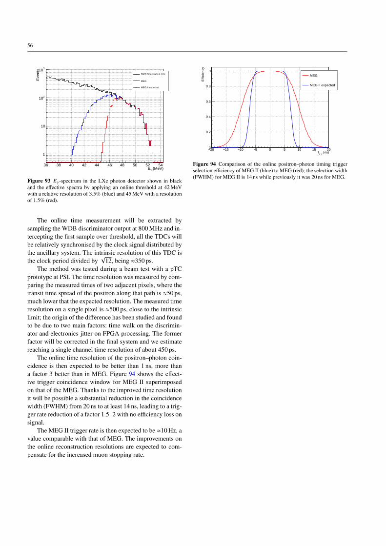
56
(MeV)γE36 38 40 42 44 46 48 50 52 54
Eve
nts
1
10
210
310RMD Spectrum in LXe
MEG
MEG II expected
Figure 93 Eγ-spectrum in the LXe photon detector shown in blackand the effective spectra by applying an online threshold at 42 MeVwith a relative resolution of 3.5% (blue) and 45 MeV with a resolutionof 1.5% (red).
The online time measurement will be extracted bysampling the WDB discriminator output at 800 MHz and in-tercepting the first sample over threshold, all the TDCs willbe relatively synchronised by the clock signal distributed bythe ancillary system. The intrinsic resolution of this TDC isthe clock period divided by
√12, being ≈350 ps.
The method was tested during a beam test with a pTCprototype at PSI. The time resolution was measured by com-paring the measured times of two adjacent pixels, where thetransit time spread of the positron along that path is ≈50 ps,much lower that the expected resolution. The measured timeresolution on a single pixel is ≈500 ps, close to the intrinsiclimit; the origin of the difference has been studied and foundto be due to two main factors: time walk on the discrimin-ator and electronics jitter on FPGA processing. The formerfactor will be corrected in the final system and we estimatereaching a single channel time resolution of about 450 ps.
The online time resolution of the positron–photon coin-cidence is then expected to be better than 1 ns, more thana factor 3 better than in MEG. Figure 94 shows the effect-ive trigger coincidence window for MEG II superimposedon that of the MEG. Thanks to the improved time resolutionit will be possible a substantial reduction in the coincidencewidth (FWHM) from 20 ns to at least 14 ns, leading to a trig-ger rate reduction of a factor 1.5–2 with no efficiency loss onsignal.
The MEG II trigger rate is then expected to be ≈10 Hz, avalue comparable with that of MEG. The improvements onthe online reconstruction resolutions are expected to com-pensate for the increased muon stopping rate.
(ns)γ+et
20− 15− 10− 5− 0 5 10 15 20
Effi
cien
cy
0
0.2
0.4
0.6
0.8
1MEG
MEG II expected
Figure 94 Comparison of the online positron–photon timing triggerselection efficiency of MEG II (blue) to MEG (red); the selection width(FWHM) for MEG II is 14 ns while previously it was 20 ns for MEG.

57
9 Expected sensitivity
The estimation of the MEG II sensitivity follows the ap-proach exploited in MEG [3]. A detailed MC simulation ofthe beam and the detector is implemented together with areconstruction of the particle’s observables. The probabilitydensity functions (PDFs) of the observables relevant for dis-criminating signal from background are generated with thehelp of simulation and prototype data. Then, an ensembleof simulated experiments (toy MC) are generated from thePDFs and analysed extracting a set of upper limits (UL). Fi-nally, the sensitivity is estimated.
9.1 Simulation and reconstruction
We developed a full simulation of the detector based onGeant4, adding information, where necessary, from meas-urements (e.g. light propagation properties in LXe) or dedic-ated simulations (e.g. ionisation density in the drift chamberfrom Garfield [151]). The Geant4 hits are then convertedinto simulated electronic signals, making use of waveformtemplates extracted from data collected with prototypes orwith the final detectors. At this stage, we also mix differentGeant4 events in order to simulate the pile-up of multiplemuon decays within the same DAQ time window.
Both data and simulated events go through the same re-construction chain. For each sub-detector, a waveform ana-lysis is performed in order to extract raw observables, suchas the signal time and charge. A hit reconstruction proced-ure is then applied to translate them into calibrated physicalobservables. The following variables are extracted:
1. the drift time of the ionisation electrons in the driftchamber and the hit position along the z-coordinate,
2. the hit time and position in each pTC and RDC PS tileand
3. the number of collected photons in each photo-sensor ofthe LXe photon detector and RDC calorimeter.
Several reconstruction algorithms are then applied to ex-tract the single particle’s observables. Most notably, dedic-ated pattern recognition algorithms and a Kalman filter tech-nique are used to extract the positron track parameters; thepositron is tracked through the pTC tiles to extract the bestestimate of the positron time; number and timing of collec-ted scintillation photons of each photo-detector in the LXephoton detector are used to extract the photon time and con-version vertex as well as the photon energy.
Finally, these observables are combined to extract thekinematic variables characterising a µ+ → e+γ decay allow-ing the discrimination from background events: the photonenergy Eγ, the positron energy Ee+ , the relative timing te+γ,and the relative polar and azimuthal angles (θe+γ, φe+γ).
Table 8 Resolutions (Gaussian σ) and efficiencies of MEG II com-pared with those of MEG
PDF parameters MEG MEG II
Ee+ (keV) 380 130θe+ (mrad) 9.4 5.3φe+ (mrad) 8.7 3.7ze+/ye+ (mm) core 2.4/1.2 1.6/0.7Eγ(%) (w>2 cm)/(w<2 cm) 2.4/1.7 1.1/1.0uγ, vγ,wγ (mm) 5/5/6 2.6/2.2/5te+γ (ps) 122 84
Efficiency (%)Trigger ≈ 99 ≈ 99Photon 63 69e+(tracking × matching) 30 70
The probability density functions (PDFs) describing thedistributions of each kinematic variable for the signal andthe backgrounds are generated relying on MC simulatedevents or on data collected from prototypes.
A representative scenario for MEG II resolutions andefficiencies is summarised in Table 8 and compared to theMEG performance. The efficiency of the positron recon-struction is greatly improved to that of MEG, thanks to thehigh efficiency of the tracking system and to the optimisedgeometry of CDCH and pTC. The resolution on the relativetime between the e+ and the γ is estimated to beσte+γ
' 84 psby adopting the most conservative estimation for the LXephoton detector timing resolution of σtγ ' 70 ps and anerror on the positron timing due to the pTC resolution ofσtpTC
e+' 31 ps, which includes an inter-counter calibration
contribution σinter-counterte+
/√
Nhit ' 10 ps, a synchronisationcontribution between WDBs of σWDB
te+' 25 ps and a contri-
bution due to the track extrapolation along the CDCH meas-ured trajectory of σCDCH
te+' 20 ps.
As an example we show the Eγ PDFs for signal (seeFig. 95) and accidental background events (see Fig. 96).The expected improvement in MEG II is visible by com-paring these PDFs (blue) with the 2010 MEG data PDFs(black). In the Eγ background PDFs various contributionsare taken into account: RMD, photons from positron AIFand from bremsstrahlung on materials in the detector, pile-up events, as well as resolution effects. The configuration ofthe CDCH, with a smaller amount of material close to theLXe photon detector, reduces the AIF contribution, which isdominant for Eγ > 52 MeV, by about 20% with respect tothe MEG detector. The combined effect of the increased res-olution and of the lower high energy background is clearlyvisible in Fig. 96.

58
Figure 95 Comparison of the Eγ PDFs for signal events based on theresolutions obtained in 2010 data (black) and on the projected valuefor the upgrade (blue).
Figure 96 Comparison of the Eγ PDFs for accidental backgroundevents based on the resolutions obtained in 2010 data (black) and onthe projected value for the upgrade (blue). Differences in relative back-ground contributions between RMD, AIF and pile-up are also takeninto account.
9.2 Analysis
Each toy MC is analysed using the maximum likelihoodanalysis technique developed following the MEG data ana-lysis [3,142,143] to extract an UL at 90% CL on the numberof signal events, following the prescription of [152], that isconverted to an UL on B(µ+ → e+γ) by using the appropri-ate normalisation factor. This technique is more efficient andreliable than a box analysis, since all types of background
weeks0 10 20 30 40 50 60 70 80 90 100
Bra
nch
in R
atio
14−10
13−10
12−10
MEG final result
MEG II in 3 years
Figure 97 Expected sensitivity of MEG II as a function of the DAQtime compared with the bounds set by MEG [3]. Assuming conservat-ively 20 DAQ weeks per year, we expect a branching ratio sensitivityof 6 × 10⁻¹⁴ in three years.
are correctly folded in the global likelihood function andtaken into account with their own statistical weights. Theenhanced precision of the MEG II detectors allows a muchbetter separation of the signal from the background and re-duces significantly the spill of the photon and positron back-ground distributions into the signal region, which is due toexperimental resolution effects.
9.3 Sensitivity estimate
An ensemble of simulated experiments (toy MC) with a stat-istics comparable to the expected number of events duringMEG II data taking are generated from the PDFs assumingzero signal events and an average number of radiative andaccidental events obtained by extrapolating the results of theMEG experiment and taking into account the new detectorperformances. The numbers of RMD and accidental eventsare then left free to fluctuate, according to Poisson statist-ics. For each toy MC we extract an UL on the B(µ+ → e+γ).Following [3], we define as sensitivity the median of the dis-tribution of the ULs obtained from the toy MCs.
In Fig. 97 we show the evolution of the sensitivity asa function of the DAQ time (in weeks). Assuming conser-vatively 140 DAQ days per year, we can reach a sensitiv-ity of 6 × 10⁻¹⁴ in three years. The sensitivity has been re-

59
evaluated since the proposal [86] according to the updatedestimations of the expected detector performances, the in-clusion of the downstream RDC and a more conservativeassumption on the DAQ time.

60
10 Conclusions
We have presented the detailed design of the components ofthe MEG II detector, together with a presentation of the sci-entific merits of the experiment. The MEG II detector res-ults from a mixture of upgraded components of the MEGexperiment (beam line, target, calibration, LXe photon de-tector) and of newly designed components (CDCH, pTC,RDC, trigger and DAQ). The design has been completed andconstruction and commissioning are ongoing.
The resolutions on the relevant physical variables areexpected to improve by about a factor of 2, as suggestedby simulation and preliminary results from laboratory andbeam tests. Those improvements, together with an increaseby more than a factor of 2 both in muon decay rate and sig-nal detection efficiency, are expected to bring the sensitivityto the µ+ → e+γ decay rate down to 6 × 10⁻¹⁴ in three yearsof data taking. In term of discriminating power of paramet-ers of models beyond the Standard Model, this limit is com-parable to those achievable by the next generation of cLFVexperiments exploiting other channels.

61
Acknowledgements
We are grateful for the support and co-operation providedby PSI as the host laboratory and to the technical andengineering staff of our institutes. This work is suppor-ted by Schweizerischer Nationalfonds (SNF) Grant 200021137738 (Switzerland), DOE DEFG02-91ER40679 (USA),INFN (Italy) and MEXT/JSPS KAKENHI Grant Num-bers JP22000004, JP25247034, JP26000004, JP15J10695,JP17J03308, JP17J04114, JP17K14267 and JSPS OverseasResearch Fellowships 2014-0066 (Japan). Partial supportof the Italian Ministry of University and Research (MIUR)Grant No. RBFR138EEU 001 is acknowledged.
References
1. J. Adam et al. The MEG detector for µ+ → e+γ decay search.Eur. Phys. J. C, 73:2365, 2013.
2. S. Ritt, R. Dinapoli, and U. Hartmann. Application of the DRSchip for fast waveform digitizing. Nucl. Instrum. Methods A,623(1):486–488, 2010.
3. A. M. Baldini et al. Search for the lepton flavour violatingdecay µ+ → e+γ with the full dataset of the MEG experiment.Eur. Phys. J. C, 76(8):434, 2016.
4. R.M. Carey et al. Proposal to search for µ−N→ e−N with asingle event sensitivity below 10−16. Fermilab proposal 0973,October 2008.
5. L. Bartoszek et al. Mu2e technical design report, October 2014.6. D. Bryman et al. An experimental search for lepton
flavor violating µ−N→ e−N conversion at sensitivityof 10−16 with a slow-extracted bunched proton beam.http://comet.kek.jp/Documents files/main-proposal.pdf, 2007.
7. R. Akhmetshin et al. COMET phase-I technical design re-port. http://http://comet.kek.jp/Documents files/IPNS-Review-2014.pdf, January 2014.
8. M. Kinsho et al. Proposal of an experimental search forµ− → e− conversion in nuclear field at sensitivity of 10−14 withpulsed proton beam from RCS. http://nasubi.hep.sci.osaka-u.ac.jp/plone/documents/deeme-proposal-r28.pdf, January 2010.
9. M. Aoki et al. An experimental search for aµ− → e− conversion at sensitivity of the order of 10−18
with a high intense muon source: PRISM. http://j-parc.jp/researcher/Hadron/en/pac 0606/pdf/p20-Kuno.pdf,2007.
10. K. Knoepfel et al. Feasibility study for a next-generation Mu2eexperiment. In APS division of particles and fields communitysummer study, Minneapolis, USA, 2013.
11. A. Blondel et al. Research proposal for an experiment to searchfor the decay µ→ 3e. arXiv::1301.6113 [hep.ex], 2013.
12. T. Aabe et al. Belle II technical design report, November 2010.13. A.G. Akeroyd et al. Physics at Super B factory, February 2010.14. A. E. Bondar. Project of super charm-tau factory at the Budker
Institute of Nuclear Physics in Novosibirsk. Phys. Atom. Nuclei,76:1072–1085, 2013.
15. Z. Hao, Z. Ren-You, H. Liang, M. Wen-Gan, G. Lei, andC. Chong. Searching for τ→ µγ lepton-flavor-violating decay atsuper charm-tau factory. Eur. Phys. J. C, 76:421, 2016.
16. H. Georgi and S. Glashow. Unity of all elementary-particleforces. Phys. Rev. Lett., 32(8):438–441, 1974.
17. U. Amaldi, W. de Boer, and H. Furstenau. Comparison of grandunified theories with electroweak and strong coupling constantsmeasured at LEP. Phys. Lett. B, 260:447–455, 1991.
18. ATLAS collaboration. Search for supersymmetry in final stateswith two same-sign or three leptons and jets using 36 fb−1
of√
s = 13 TeV pp collision data with the ATLAS detector.J. High Energy Phys., 09:084, 2017.
19. Albert M. Sirunyan et al. Search for supersymmetry in pp col-lisions at
√s = 13 TeV in the single-lepton final state using the
sum of masses of large-radius jets. Phys. Rev. Lett., 119:151802,2017.
20. Y. Fukuda et al. Evidence for oscillation of atmospheric neutri-nos. Phys. Rev. Lett., 81(8):1562, 1998.
21. Q. R. Ahmad et al. Direct evidence for neutrino flavor transform-ation from neutral-current interactions in the Sudbury NeutrinoObservatory. Phys. Rev. Lett., 89(1):011301, 2002.
22. C. Patrignani et al. Review of particle physics. Chinese Phys. C,40(10):100001, 2016.
23. P. Mikowski. µ→ eγ at a rate of one out of 109 muon decays?Phys. Lett. B, 67(4):421–428, 1977.
24. T. Yanagida. Horizontal gauge symmetry and masses of neutri-nos. In A. Sawada and A. Sugamoto, editors, Proceedings Work-shop on Unified Theories and Baryon Number in the Universe,pages 95–98, Tsukuba, Japan, 1979.
25. M. Gell-Mann, P. Ramond, and R. Slansky. Complex spinors andunified theories. In P. Van Nieuwenhuizen and D. Z. Freedman,editors, Proceedings Supergravity Workshop at Stony Brook,pages 315–321, New York, USA, 1979. North-Holland Pub. Co.
26. R. N. Mohapatra and G. Senjanovic. Neutrino mass and spontan-eous parity nonconservation. Phys. Rev. Lett., 44(14):912–915,1980.
27. R. N. Mohapatra et al. Theory of neutrinos: a white paper. Rep.Prog. Phys., 70:1757–1867, 2007.
28. M. Fukugita and T. Yanagida. Baryogenesis without grand uni-fication. Phys. Lett. B, 174(1):45–47, 1986.
29. J. Ellis and D. V. Nanopoulos. Flavour-changing neutral in-teractions in broken supersymmetric theories. Phys. Lett. B,110(1):44–48, 1982.
30. B. A. Campbell. Supersymmetry and neutral-flavor nonconser-vation. Phys. Rev. D, 28(1):209–216, 1983.
31. I.-H. Lee. Lepton number violation in softly broken supersym-metry. Phys. Lett. B, 138(1-3):121–127, 1984.
32. F. Gabbiani, E. Garbrielli, A. Masiero, and L. Silvestrini. A com-plete analysis of FCNC and CP constraints in general SUSY ex-tensions of the standard model. Nucl. Phys. B, 477(2):321–352,1996.
33. W. Altmannshofer, A. J. Buras, S. Gori, P. Paradisi, and D. M.Straub. Anatomy and phenomenology of FCNC and CPV effectsin SUSY theories. Nucl. Phys. B, 830(1-2):17–94, 2010.
34. M. Arana-Catania, S. Heinemeyer, and M. J. Herrero. Newconstraints on general slepton flavor mixing. Phys. Rev. D,88(1):015026, 2013.
35. W. Altmannshofer, R. Harnik, and J. Zupan. Low energy probesof PeV scale sfermions. J. High Energy Phys., 11:202, 2013.
36. L. J. Hall, V. A. Kostelecky, and S. Raby. New flavor violationsin supergravity models. Nucl. Phys. B, 267:415–432, 1986.
37. F. Borzumati and A. Masiero. Large muon- and electron-numbernonconservation in supergravity theories. Phys. Rev. Lett.,57(8):961–964, 1986.
38. A. Masiero, S. K. Vempati, and O. Vives. Seesaw and leptonflavour violation in SUSY SO(10). Nucl. Phys. B, 649(1-2):189–204, 2003.
39. R. Barbieri and L. J. Hall. Signals for supersymmetric unifica-tion. Phys. Lett. B, 338(2–3):212–218, 1994.
40. R. Barbieri, L. Hall, and A. Strumia. Violations of lepton fla-vour and CP in supersymmetric unified theories. Nucl. Phys. B,445(2–3):219–251, 1995.
41. P. Ciafaloni, A. Romanino, and A. Strumia. Lepton flavour viol-ations in SO(10) with large tanβ. Nucl. Phys. B, 458(1–2):3–22,1996.

62
42. J. Hisano, T. Moroi, K. Tobe, and M. Yamaguchi. Exact eventrates of lepton flavor violating processes in supersymmetricSU(5) model. Phys. Lett. B, 458:341–350, 1997. Erratum ibid.397 (1997) 357.
43. J. Hisano, T. Moroi, K. Tobe, M. Yamaguchi, and T. Yanagida.Lepton-flavor violation in the supersymmetric standard modelwith seesaw-induced neutrino masses. Phys. Lett. B, 357:579–587, 1995.
44. J. Hisano, T. Moroi, K. Tobe, and M. Yamaguchi. Lepton-flavorviolation via right-handed neutrino Yukawa couplings in the su-persymmetric standard model. Phys. Rev. D, 53(5):2442–2459,Mar 1996.
45. J. Hisano and D. Nomura. Solar and atmospheric neutrino os-cillations and lepton flavor violation in supersymmetric modelswith right-handed neutrinos. Phys. Rev. D, 59(11):116005, 1999.
46. J. A. Casas and A. Ibarra. Oscillating neutrinos and µ→ eγ.Nucl. Phys. B, 618(1-2):171–204, 2001.
47. S. T. Petcov. The processes µ→ eγ, µ→ 3e, ν′ → ν + γ inthe Weinberg-Salam model with neutrino mixing. Sov. J. Nucl.Phys., 25:340, 1977. Erratum ibid. 25 (1977) 698.
48. T. P. Cheng and Li.-F. Li. µ→ eγ in theories with Dirac andMajorana neutrino-mass terms. Phys. Rev. Lett., 45(24):1908–1911, 1980.
49. G. Aad et al. Observation of a new particle in the search forthe Standard Model Higgs boson with the ATLAS detector at theLHC. Phys. Lett. B, 716(1):1–29, 2012.
50. S. Chatrchyan et al. Observation of a new boson at a mass of125 GeV with the CMS experiment at the LHC. Phys. Lett. B,716(1):30–61, 2012.
51. F. P. An et al. Observation of electron-antineutrino disappearanceat Daya Bay. Phys. Rev. Lett., 108(17):171803, 2012.
52. J.K. Ahn et al. Observation of reactor electron antineutrinodisappearance in the RENO experiment. Phys. Rev. Lett.,108(19):191802, 2012.
53. K. Abe et al. Indication of electron neutrino appearancefrom an accelerator-produced off-axis muon neutrino beam.Phys. Rev. Lett., 107(4):041801, 2011.
54. Y. Abe et al. Indication for the disappearance of reactor electronantineutrinos in the Double Chooz experiment. Phys. Rev. Lett.,108(13):131801, 2012.
55. G. Aad et al. Combined measurement of the Higgs boson massin pp collisions at
√s = 7 and 8 TeV with the ATLAS and CMS
experiments. Phys. Rev. Lett., 114(19):191803, 2015.56. S. Akula, B. Altunkaynak, D. Feldman, P. Nath, and G. Peim.
Higgs boson mass predictions in SUGRA unification, recentLHC-7 results and dark matter. Phys. Rev. D, 85(7):075001,2012.
57. Y. Amhis et al. Averages of b-hadron, c-hadron, and τ-leptonproperties as of summer 2016, 2016.
58. V. Khachatryan et al. Observation of the rare B0s → µ+µ− decay
from the combined analysis of CMS and LHCb data. Nature,522:68–72, 2015.
59. L. Calibbi, D. Chowdhury, A. Masiero, K.M. Patel, and S.K.Vempati. Status of supersymmetric type-I seesaw in SO(10) in-spired models. J. High Energy Phys., 2012(11):040, 2012.
60. M. Hisrsh, F. R. Joaquim, and A. Vicente. Constrained SUSYseesaws with a 125 GeV Higgs. J. High Energy Phys.,2012(11):105, 2012.
61. M. Cannoni, J. Ellis, Gomez, and Z. Lola. Neutrino textures andcharged lepton flavour violation in light of θ13, MEG and LHCdata. Phys. Rev. D, 88(7):075005, 2013.
62. B. Dutta, Y. Mimura, and R. N. Mohapatra. Proton decay andµ+ → e+γ connection in a renormalizable SO(10) GUT for neut-rinos. Phys. Rev. D, 87(7):075008, 2013.
63. D. Chowdhury and K. M. Patel. Revisiting lepton flavor violationin supersymmetric type-II seesaw. Phys. Rev. D, 87(9):095018,2013.
64. T. Moroi, M. Nagai, and T. T. Yanagida. Lepton-flavor violationsin high-scale SUSY with right-handed neutrions. Phys. Lett. B,728:342–346, 2014.
65. T. Goto and Y. Okada. Lepton flavor violation in the supersym-metric seesaw model after the LHC 8 TeV run. Phys. Rev. D,91(3):033007, 2015.
66. K. Bora and G. Ghosh. Charged lepton flavor violation µ→ eγ inµ–τ symmetric SUSY SO(10) mSUGRA, NUHM, NUGM, andNUSM theories and LHC. Eur. Phys. J. C, 75:428, 2015.
67. T. Fukuyama, K. Ichikawa, and Y. Mimura. Revisiting fermionmass and mixing fits in the minimal SUSY SO(10) GUT model.Phys. Rev. D, 94(7):075018, 2016.
68. K. Agashe, A. E. Blechman, and F. Petriello. Probing theRandall-Sundrum geometric origin of flavor with lepton flavorviolation. Phys. Rev. D, 74(5):053011, 2006.
69. A. M. Iyer and S. K. Vempati. Lepton masses and flavor violationin Randall Sundrum model. Phys. Rev. D, 86(5):056005, 2012.
70. M. Beneke, P. Moch, and J. Rohrwild. Lepton flavour viola-tion in RS models with a brane- or nearly brane-localized Higgs.Nucl. Phys. B, 906:561–614, 2016.
71. V. Cirigliano, A. Kurylov, M. J. Ramsey-Musolf, and P. Vogel.Lepton flavor violation without supersymmetry. Phys. Rev. D,70(7):075007, 2004.
72. A. G. Akeroyd, M. Aoki, and Y. Okada. Lepton flavor violat-ing τ decays in the left-right symmetric model. Phys. Rev. D,76(1):013004, 2007.
73. C.-H. Lee, P. S. Bhupal Dev, and R. N. Mohapatra. NaturalTeV-scale left-right seesaw mechanism for neutrinos and experi-mental tests. Phys. Rev. D, 88(9):093010, 2013.
74. P. F. Perez and C. Murgui. Lepton flavor violation in left-righttheory. Phys. Rev. D, 95(7):075010, 2017.
75. R. Benbrik and C.-K. Chua. Lepton flavor violating l → l′γand z → ll′ decays induced by scalar leptoquarks. Phys. Rev. D,78(7):075025, 2008.
76. J. M. Arnold, B. Fornal, and M. B. Wise. Phenomenology ofscalar leptoquarks. Phys. Rev. D, 88(3):035009, 2013.
77. B. Gripaios, M. Nardecchia, and S. A. Renner. Compositeleptoquarks and anomalies in B-meson decays. J. High En-ergy Phys., 2015(05):006, 2015.
78. I. de Medeiros Varzielas and G. Hiller. Clues for flavor from rarelepton and quark decays. J. High Energy Phys., 2015(06):072,2015.
79. S. R. Choudhury, A. S. Cornell, A. Deandrea, N. Gaur, andA. Goyal. Lepton flavour violation in the little Higgs model withT parity. Phys. Rev. D, 75(5):055011, 2007.
80. M. Blanke, J. A. Buras, B. Duling, S. Recksiegel, and C. Tarant-ino. FCNC processes in the littlest Higgs model with T-parity:An update. Acta Phys. Polon. B, 41(3):657–683, 2010.
81. F. del Aguila, J. I. Illana, and M. D. Jenkins. Lepton flavor vi-olation in the simplest little Higgs model. J. High Energy Phys.,2011(03):080, 2011.
82. L. Wang and X.-F. Han. Lepton flavor-violating processes in thesimplest little Higgs model: e+e−(γγ) → li l j under new boundfrom li → l jγ. Phys. Rev. D, 85(1):013011, 2012.
83. A. Crivellin, S. Davidson, G. M. Pruna, and A. Signer.Renormalization-group improved analysis of µ− → e− processesin a systematic effective-field-theory approach. J. High En-ergy Phys., 2017(05):117, 2017.
84. Y. Kuno and Y. Okada. Muon decay and physics beyond thestandard model. Rev. Mod. Phys., 73(1):151–202, 2001.
85. A. Czarnecki, W. J. Marciano, and K. Melnikov. Coherent muon–electron conversion in muonic atoms. In AIP Conf. Proc., editor,Proceedings of workshop on physics at the first muon colliderand at the front end of a muon collider, pages 409–418, 1998.
86. A. M. Baldini, F. Cei, C. Cerri, S. Dussoni, L. Galli, M. Grassi,et al. MEG upgrade proposal, December 2013.

63
87. A. M. Baldini et al. Muon polarization in the MEG experiment:predictions and measurements. Eur. Phys. J. C, 76(4):223, 2016.
88. A. Buhler et al. Measurements of muon depolarization in severalmaterials. Nuovo Cimento, 39(3):824–828, 1965.
89. A. E. Pifer, K. Browen, and K. R. Kendall. A high stoppingdensity µ+ beam. Nucl. Instrum. Methods, 135:39–46, 1976.
90. Saint-Gobain Ceramics & Plastics, Inc. Plastic scintillatingfibers.
91. Hamamatsu Photonics K. K. MPPC S13360-1350CS.92. Yu. M. Protopopov and V. G. Vasil’chenko. Radiation damage in
plastic scintillators and optical fibers. Nucl. Instrum. Methods B,95:496–500, 1995.
93. M. Cascella, F. Grancagnolo, and G. Tassielli. Cluster count-ing/timing techniques for drift chambers. Nucl. Phys. B (Proc.Suppl.), 248-250:127–130, 2014.
94. A. M. Baldini et al. Single-hit resolution measurement withMEG II drift chamber prototypes. J. Instrum., 11:P07011, July2016.
95. G. Cataldi, F. Grancagnolo, and S. Spagnolo. Results from acluster counting measurement in helium-hydrocarbon mixture.Technical Report 155, KLOE, Feb 1996.
96. G. Chiarello, C. Chiri, A. Corvaglia, F. Grancagnolo, M. Panareo,A. Pepino, C. Pinto, and G. Tassielli. A high performance FrontEnd Electronics for drift chamber readout in MEG experimentupgrade. Nucl. Instrum. Methods A, 824:336–339, 2016.
97. G. Chiarello, C. Chiri, A. Corvaglia, F. Grancagnolo, M. Panareo,A. Pepino, C. Pinto, and G. Tassielli. A high performance frontend for MEG II tracker. In Proceedings 6th IEEE Int. Workshopon Advances in Sensors and Interfaces (IWASI 2015), pages 55–57, Gallipoli, Italy, 2015.
98. Analog Devices, Inc. ADA4927 datasheet ultralow distortioncurrent feedback differential ADC driver.
99. Texas Instruments. THS4509 datasheet wideband, low-noise,low-distortion, fully-differential amplifier.
100. L Galli, U Hartmann, F Morsani, D Nicol, and S Ritt. A new gen-eration of integrated trigger and read out system for the MEG IIexperiment. In 2014 IEEE Nuclear Science Symposium and Med-ical Imaging Conference (NSS/MIC), pages 1–3. IEEE, 2014.
101. Mini-SAS HD Next generation SAS storage interface.102. G. Chiarello et al. A new construction technique of high granu-
larity and high transparency drift chambers for modern high en-ergy physics experiments. Nucl. Instrum. Methods A, 824:512–514, 2016.
103. National Instruments. CompactRIO platform.104. Dr. Mergenthaler GmbH.105. M. Venturini. Improving the search for the µ→ eγ decay: the fi-
nal MEG results and the new tracker for its upgrade. PhD Thesis,Scuola Normale Superiore - Pisa, 2017.
106. DEA Ghibli.107. L. Galli et al. A silicon-based cosmic ray telescope as an external
tracker to measure detector performance. IEEE Trans. Nucl. Sci.,62(1):395–402, 2015.
108. T. Sugitate, Y. Akiba, S. Hayashi, Y. Miake, S. Nagamiya, andM. Torikoshi. 100 cm long time-of-flight scintillation counterswith rms resolution of 50 ps. Nucl. Instrum. Methods A, 249(2–3):354–360, September 1986.
109. Y. Shikaze, S. Orito, T. Mitsui, K. Yoshimura, H. Matsumoto,H. Matsunaga, M. Nozaki, et al. Large-area scintillator hodo-scope with 50 ps timing resolution onboard BESS. Nucl. In-strum. Methods A, 455(3):596–606, December 2000.
110. M. De Gerone, S. Dussoni, K. Fratini, F. Gatti, R. Valle, et al.Development and commissioning of the Timing Counter for theMEG Experiment. IEEE Trans. Nucl. Sci., 59:379–388, 2012.
111. A. Stoykov, R. Scheuermann, and K. Sedlak. A time resolu-tion study with a plastic scintillator read out by a Geiger-modeavalanche photodiode. Nucl. Instrum. Methods A, 695:202–205,December 2012.
112. W. Ootani. Development of pixelated scintillation detector forhighly precise time measurement in MEG upgrade. Nucl. In-strum. Methods A, 732:146–150, December 2013.
113. M. De Gerone et al. Design and test of an extremely high res-olution Timing Counter for the MEG II experiment: preliminaryresults. J. Instrum., 9:C02035, 2014.
114. P. W. Cattaneo, Matteo De Gerone, Flavio Gatti, Miki Nishimura,Wataru Ootani, et al. Development of high precision tim-ing counter based on plastic scintillator with SiPM readout.IEEE Trans. Nucl. Sci., 61(5):2657–2666, 2014.
115. Miki Nishimura et al. Pixelated positron timing counter withSiPM-readout scintillator for MEG II experiment. In Proceed-ings 4th Int. Conf. on New Photo-Detectors, page PoS(PhotoDet2015)011, Moscow, Russia,, July 2016.
116. Saint-Gobain Ceramics & Plastics, Inc. BC-418, BC-420, BC-422 Premium Plastic Scintillators.
117. R. A. Lerche and D. W. Phillon. Rise time of BC-422 plasticscintillator < 20 ps. In Conference Record 1991 IEEE Nuc-lear Science Symposium and Medical Imaging Conference, pages167–170, Santa Fe, NM, November 1991.
118. Y. Benhammou et al. Beam test results with fast preamplifiersassociated to APDs readout of PbWO4 crystal. Tech. Note 95-122, CMS, September 1995.
119. R. Scheuermann, A. Stoykov, D. Renker, Z. Sadygov, R. Me-htieva, A. Dovlatov, and V. Zhuk. Scintillation detectors foroperation in high magnetic fields: Recent development basedon arrays of avalanche microchannel photodiodes. Nucl. In-strum. Methods A, 581:443–446, October 2007.
120. S. Agostinelli et al. Geant4—a simulation toolkit. Nucl. In-strum. Methods A, 506:250–303, 2003.
121. J. Allison et al. Geant4 developments and applications.IEEE Trans. Nucl. Sci., 53:270–278, 2006.
122. J. Allison et al. Recent develpments in Geant4. Nucl. In-strum. Methods A, 835:186–225, 2016.
123. Y. Uchiyama, Gianluigi Boca, P. W. Cattaneo, M. De Gerone,F. Gatti, M. Nakao, M. Nishimura, W. Ootani, G. Pizzigoni,M. Rossella, M. Simonetta, and K. Yoshida. 30-ps time resol-ution with segmented scintillation counter for MEG II. Nucl. In-strum. Methods A, 845:507–510, 2017.
124. R. Bertoni, M. Bonesini, A. de Bari, and M. Rossella. A laserdiode based system for calibration of fast time-of-flight detectors.J. Instrum., 11(05):P05024, 2016.
125. Hamamatsu Photonics K. K. Picosecond light source PLP-10.126. Piezosystem JENA.127. Lightel. Multimode coupler MMC-1-A-EVEN-1-A-30CM-R-1.128. P. W. Cattaneo, M. De Gerone, F. Gatti, M. Nishimura,
W. Ootani, M. Rossella, S. Shirabe, and Y. Uchiyama. Time res-olution of time-of-flight detector based on multiple scintillationcounters readout by SiPMs. Nucl. Instrum. Methods A, 828:191–200, 2016.
129. A. Stoykov. Private communication.130. W. Ootani et al. Development of deep-UV sensitive MPPC for
liquid xenon scintillation detector. Nucl. Instrum. Methods A,A787:220–223, 2015.
131. M. Yokoyama, T. Nakaya, S. Gomi, A. Minamino, N. Nagai,et al. Mass production test of Hamamatsu MPPC for T2K neut-rino oscillation experiment. Nucl. Instrum. Methods A, 610:362–365, 2009.
132. Jozsef Janicsko Csathy, Hossein Aghaei Khozani, Xiang Liu,Bela Majorovits, and Allen Caldwell. Development of an anti-Compton veto for HPGe detectors operated in liquid argon usingsilicon photo-multipliers. Nucl. Instrum. Methods A, 654:225–232, 2011.
133. T. Matsumura et al. Radiation damage to MPPCs by irradi-ation with protons. In Proceedings Int. Workshop New Photon-Detectors, page PoS(PD07)033, Kobe, Japan, June 2007.

64
134. T. Matsubara, H. Tanaka, K. Nitta, and M. Kuze. Radiation dam-age of MPPC by gamma-ray irradiation with Co-60. In Proceed-ings Int. Workshop New Photon-Detectors, page PoS(PD07)032,Kobe, Japan, 2007.
135. V. Andreev et al. A high granularity scintillator hadronic-calorimeter with SiPM readout for a linear collider detector.Nucl. Instrum. Methods A, 540:368–380, 2005.
136. Hamamatsu Photonics K. K. Quartz transmittance.137. Ltd. JYEBAO Co.138. Cryomech, Inc. AL300 Cryorefrigerator.139. J. Spuller, D. Berghofer, M.D Hasinoff, R. Macdonald, D.F.
Measday, M. Salomon, T. Suzuki, R. Poutissou, J.-M. Poutis-sou, and J.K.P. Lee. A remeasurement of the Panofsky ratio.Phys. Lett. B, 67(4):479–482, 1977.
140. Hamamatsu Photonics K. K. MPPC S13360-3050PE.141. Hamamatsu Photonics K. K. MPPC S12572-025.142. J. Adam et al. New limit on the lepton-flavor-violating decay
µ+ → e+γ. Phys. Rev. Lett., 107:171801, 2011.143. J. Adam et al. New constraint on the existence of the µ+ → e+γ
decay. Phys. Rev. Lett., 110:201801, 2013.144. S. Ritt. The DRS chip: cheap waveform digitizing in the GHz
range. Nucl. Instrum. Methods A, 518(1-2):470–471, Feb 2004.145. Texas Instruments. LMK03000, precision clock conditioner.146. Xilinx.147. Diodes Incorporated.148. Maxim Integrated.149. MSCB protocol.150. Maxim Integrated. 1-Wire.151. Garfield – simulation of gaseous detectors.152. G. J. Feldman and R. D. Cousins. Unified approach to the
classical statistical analysis of small signals. Phys. Rev. D,57(7):3873–3889, Apr 1998.