· The BMP3 90 is a digital sensor with pressure and temperature measurement based on proven...
59
BMP390L –Datasheet Document revision 1.2 Document release date February 2020 Document number BST-BMP390L-DS001-02 Technical reference code(s) 0273 017 023 Notes Data and descriptions in this document are subject to change without notice. Product photos and pictures are for illustration purposes only and may differ from the real product appearance. BMP390L Digital pressure sensor
Transcript of · The BMP3 90 is a digital sensor with pressure and temperature measurement based on proven...
Bosch Sensortec | BMP390L Datasheet 1 | 59
Modifications reserved |Data subject to change without notice | Printed in Germany Document number: BST-BMP390L-DS001-02 Revision_1.2_022020
BMP390L –Datasheet Document revision 1.2
Document release date February 2020
Document number BST-BMP390L-DS001-02
Technical reference code(s) 0273 017 023
Notes Data and descriptions in this document are subject to change without notice. Product photos and pictures are for illustration purposes only and may differ from the real product appearance.
BMP390L Digital pressure sensor

Bosch Sensortec | BMP390L Datasheet 2 | 59
Modifications reserved |Data subject to change without notice | Printed in Germany Document number: BST-BMP390L-DS001-02 Revision_1.2_022020
BMP390 Digital pressure sensor
The BMP390 is a digital sensor with pressure and temperature measurement based on proven sensing principles. The sensor module is housed in an extremely compact 10-pin metal-lid LGA package with a footprint of only 2.0 × 2.0 mm² and max 0.8 mm package height. Its small dimensions and its low power consumption of 3.2 µA @1Hz allow the implementation in battery driven devices such as mobile phones, GPS modules or watches.
Typical applications
• Vertical velocity indication (e.g. rise/sink speed) • Internet of things • Enhancement of GPS navigation (e.g. time-to-first-fix improvement, dead-reckoning, slope detection) • Indoor navigation & localization (floor detection, elevator detection) • Outdoor navigation, leisure and sports applications • Weather forecast • Health care applications (e.g. spirometry) • Fitness applications like enhancement of calorie detection • AR & VR applications • Context awareness
Target Devices
• Flying toys • Drones • Handsets such as mobile phones, tablet PCs, GPS devices • Navigation systems • Portable health care devices • Home weather stations • Watches • White goods
Bosch Sensortec | BMP390L Datasheet 3 | 59
Modifications reserved |Data subject to change without notice | Printed in Germany Document number: BST-BMP390L-DS001-02 Revision_1.2_022020
Key features
Table 1: Key Features of BMP390 Package 2.0 mm x 2.0 mm x 0.75 mm metal lid LGA
Digital interface I²C (up to 3.4 MHz) and SPI (3 and 4 wire, up to 10 MHz)
Supply voltage VDD main supply voltage range: 1.65 V to 3.6 V
VDDIO interface voltage range: 1.2 V to 3.6 V
Relative accuracy typ. ± 3 Pa, equiv. to ± 0.25 m
(700 … 1100 hPa, 25 . . . 40 °C )
Absolute accuracy typ. ± 50 Pa
(300 ...1100 hPa, -0 ...+65 °C)
Temperature coefficient offset mean value ± 0.6 Pa/K (25 – 40°C @900 hPa)
Current consumption 3.2 µA at 1 Hz pressure and temperature
1.4 µA in sleep mode
Operating range -40 ‒ +85 °C, 300‒1250 hPa
The product is RoHS compliant, halogen-free, MSL1
BMP390 enables accurate altitude tracking and is specifically suited for mobile applications. The best-in-class TCO between -20-65°C for accurate altitude measurement over a wide temperature range of the BMP390 greatly enhance use cases like indoor navigation and localization. It is compatible for use with other Bosch sensors, including the IMUs like BMI260 for better performance, robustness and stability. The new BMP390 sensor offers outstanding design flexibility, providing a single package solution that can also be easily integrated into other existing and upcoming devices such as smartphones, wearables smart homes and industrial products. The sensor is more accurate than its predecessor BMP380, covering a wide measurement range from 300 hPa to 1250 hPa. This new barometric pressure sensor exhibits an attractive price-performance ratio coupled with low power consumption. It is available in a compact 10-in 2.0 x 2.0 x 0.75 mm³ LGA package with metal lid Due to the built-in hardware synchronization of the pressure sensor data and its ability to synchronize data from external devices such as acceleration sensors, the BMP390 is ideally suited for fitness and navigation applications which require highly accurate, low power and low latency sensor data fusion. The new interrupt functionality provides simple access to data and storage. Examples of interrupts than can be used in a power efficient manner without using software algorithms include: Data ready interrupt, watermark interrupt (on byte level) or FIFO full interrupt. BMP390 also includes a new FIFO functionality. This greatly improves ease of use while helping to reduce power consumption of the overall device system during full operation. The integrated 512 byte FIFO buffer supports low power applications and prevents data loss in non-real-time systems.

Bosch Sensortec | BMP390L Datasheet 4 | 59
Modifications reserved |Data subject to change without notice | Printed in Germany Document number: BST-BMP390L-DS001-02 Revision_1.2_022020
Table of Contents
1. Specification ..................................................................................................................................................................... 7
2. Absolute maximum ratings ............................................................................................................................................. 9
3. Functional description .................................................................................................................................................... 9 3.1. Block diagram ......................................................................................................................................................... 10 3.2. Power management ................................................................................................................................................ 11 3.3. Power modes .......................................................................................................................................................... 11
3.3.1. Sleep mode ...................................................................................................................................................... 11 3.3.2. Forced mode ..................................................................................................................................................... 11 3.3.3. Normal mode ..................................................................................................................................................... 12 3.3.4. Mode transition diagram .................................................................................................................................... 13
3.4. Measurement flow .................................................................................................................................................. 13 3.4.1. Pressure measurement ..................................................................................................................................... 14 3.4.2. Temperature measurement ............................................................................................................................... 14 3.4.3. IIR filter .............................................................................................................................................................. 15 3.4.4. Oversampling .................................................................................................................................................... 15
3.5. Filter selection ........................................................................................................................................................ 17 3.6. FIFO Description ..................................................................................................................................................... 18
3.6.1. FIFO input data ................................................................................................................................................. 18 3.6.2. FIFO data sampling selection............................................................................................................................ 18 3.6.3. FIFO read out .................................................................................................................................................... 18 3.6.4. FIFO overflow behavior ..................................................................................................................................... 19 3.6.5. FIFO Frames ..................................................................................................................................................... 19 3.6.7. FIFO flush conditions ........................................................................................................................................ 21
3.7. Interrupts ................................................................................................................................................................. 22 3.7.1. Interrupt default mode ....................................................................................................................................... 22 3.7.2. Interrupt pin latching .......................................................................................................................................... 22 3.7.3. Monitoring .......................................................................................................................................................... 22 3.7.4. Interrupt Pin Configuration ................................................................................................................................ 22 3.7.5. Interrupt functions .............................................................................................................................................. 23
3.8. Current consumption ............................................................................................................................................. 26 3.9. Measurement timings ............................................................................................................................................. 26
3.9.1. Measurement time ............................................................................................................................................. 26 3.9.2. Measurement rate in forced mode and normal mode ....................................................................................... 27
3.10. Data readout from data registers ...................................................................................................................... 27 3.10.1. Data register shadowing .................................................................................................................................... 27
3.11. Output compensation ......................................................................................................................................... 28 3.11.1. Memory Map Trimming Coefficients .................................................................................................................. 28
4. Global memory map and register description ............................................................................................................ 29 4.1. General remarks ..................................................................................................................................................... 29 4.2. Datasheet Memory Map ......................................................................................................................................... 29 4.3. Register description ............................................................................................................................................... 31
4.3.1. Register 0x00 “CHIP_ID” ................................................................................................................................... 31 4.3.2. Register 0x01 “REV_ID” .................................................................................................................................... 31 4.3.3. Register 0x02 “ERR_REG” ............................................................................................................................... 31 4.3.4. Register 0x03 “STATUS” ................................................................................................................................... 32 4.3.5. Register 0x04 .. 0x06 Pressure Data ................................................................................................................ 32 4.3.6. Register 0x07 .. 0x09 Temperature Data .......................................................................................................... 32 4.3.7. Register 0x0C .. 0x0E Sensor Time .................................................................................................................. 33 4.3.8. Register 0x10 “EVENT” ..................................................................................................................................... 33 4.3.9. Register 0x11 “INT_STATUS” ............................................................................................................................ 33 4.3.10. Register 0x12 .. 0x13 “FIFO_LENGTH” ............................................................................................................ 33

Bosch Sensortec | BMP390L Datasheet 5 | 59
Modifications reserved |Data subject to change without notice | Printed in Germany Document number: BST-BMP390L-DS001-02 Revision_1.2_022020
4.3.11. Register 0x14 “FIFO_DATA” ............................................................................................................................. 34 4.3.12. Register 0x15 .. 0x16 FIFO Watermark ............................................................................................................. 34 4.3.13. Register 0x17 “FIFO_CONFIG_1”..................................................................................................................... 34 4.3.14. Register 0x18 “FIFO_CONFIG_2”..................................................................................................................... 35 4.3.15. Register 0x19 “INT_CTRL” ................................................................................................................................ 35 4.3.16. Register 0x1A “IF_CONF” ................................................................................................................................. 37 4.3.17. Register 0x1B “PWR_CTRL” ............................................................................................................................. 37 4.3.18. Register 0x1C “OSR” ........................................................................................................................................ 38 4.3.19. Register 0x1D “ODR” ........................................................................................................................................ 38 4.3.20. Control settings for odr_sel ............................................................................................................................... 39 4.3.21. Register 0x1F “CONFIG” ................................................................................................................................... 40 4.3.22. Register 0x30 .. 0x57 “calibration data” ............................................................................................................ 40 4.3.23. Register 0x7E “CMD” ........................................................................................................................................ 40
5. Digital interfaces ............................................................................................................................................................ 41 5.1. Interface selection .................................................................................................................................................. 41 5.2. I²C Interface ............................................................................................................................................................. 41
5.2.1. I²C write ............................................................................................................................................................. 42 5.2.2. I²C read .............................................................................................................................................................. 42
5.3. SPI interface ............................................................................................................................................................ 43 5.3.1. SPI write ............................................................................................................................................................ 43 5.3.2. SPI read ............................................................................................................................................................. 44
5.4. Interface parameter specification ......................................................................................................................... 44 5.4.1. General interface parameters............................................................................................................................ 44 5.4.2. I²C timings ......................................................................................................................................................... 44 5.4.3. SPI timings ........................................................................................................................................................ 46
6. Pin-out and connection diagram .................................................................................................................................. 47 6.1. Pin-out ..................................................................................................................................................................... 47 6.2. Connection diagram ¾-wire SPI ............................................................................................................................ 48 6.3. Connection diagram I²C ......................................................................................................................................... 49
7. Package, reel and environment .................................................................................................................................... 50 7.1. Outline dimensions ................................................................................................................................................ 50 7.2. Landing pattern....................................................................................................................................................... 50 7.3. Marking .................................................................................................................................................................... 51
7.3.1. Mass production samples .................................................................................................................................. 51 7.3.2. Engineering samples ......................................................................................................................................... 51
7.4. Soldering guidelines .............................................................................................................................................. 52 7.5. Tape and reel specification .................................................................................................................................... 53
7.5.1. Dimensions ........................................................................................................................................................ 53 7.5.2. Orientation within the reel .................................................................................................................................. 53
7.6. Mounting and assembly recommendations ........................................................................................................ 53 7.7. Environmental safety ............................................................................................................................................. 54
7.7.1. RoHS ................................................................................................................................................................. 54 7.7.2. Halogen content ................................................................................................................................................ 54 7.7.3. Internal package structure ................................................................................................................................. 54
8. Legal disclaimer ............................................................................................................................................................. 55 8.1. Engineering samples ............................................................................................................................................. 55 8.2. Product use ............................................................................................................................................................. 55 8.3. Application examples and hints ............................................................................................................................ 55
Appendix: Computation formulae reference implementation .......................................................................................... 56 8.4. Calibration coefficient ............................................................................................................................................ 56

Bosch Sensortec | BMP390L Datasheet 6 | 59
Modifications reserved |Data subject to change without notice | Printed in Germany Document number: BST-BMP390L-DS001-02 Revision_1.2_022020
8.5. Temperature compensation ................................................................................................................................... 56 8.6. Pressure compensation ......................................................................................................................................... 57
9. Document history and modification ............................................................................................................................ 58

Bosch Sensortec | BMP390L Datasheet 7 | 59
Modifications reserved |Data subject to change without notice | Printed in Germany Document number: BST-BMP390L-DS001-02 Revision_1.2_022020
1. Specification If not stated otherwise,
• All values are valid over the full voltage range • All minimum/maximum values are given for the full accuracy temperature range • Minimum/maximum values of drifts, offsets and temperature coefficients are ±3σ values over lifetime • Typical values of currents and state machine timings are determined at 25 °C • Typical values of currents and state machine timings are determined at 25°C, minimum/maximum values of currents
are determined at -40°C/85°C. • Minimum/maximum values of state machine timings are determined using corner lots over 0…+65 °C temperature
range.
Table 2: General electrical parameter specifications OPERATING CONDITIONS BMP390
Parameter Symbol Condition Min Typ Max Unit
Operating temperature range TA
operational -40 25 +85 °C
full accuracy 0 +65
Operating pressure range P full accuracy 300 1250 hPa
Sensor supply voltage VDD ripple max. 50mVpp 1.65 1.8 3.6 V
Interface supply voltage VDDIO 1.2 1.8 3.6 V
Sleep current IDDSL VDD = VDDIO = 1.8 V 1.4 µA
IDDSL VDD = VDDIO = 3.6 V 1.5 µA
Peak current Ipeak during pressure measurement 660 730 µA
Peak current IDDT during temperature measurement 240 320 µA
Relative accuracy pressure1 Arel
700 . . . 1100 hPa 25 . . . 40 °C, 10 kPa steps
±0.03 hPa
+/-25 cm cm
Offset temperature coefficient4 TCO
900 hPa 25 . . . 40 °C ±0.62 Pa/K
Absolute accuracy APfull 900 hPa
25 °C ±0.33 hPa
1 Per 10kPa steps 2 Mean value

Bosch Sensortec | BMP390L Datasheet 8 | 59
Modifications reserved |Data subject to change without notice | Printed in Germany Document number: BST-BMP390L-DS001-02 Revision_1.2_022020
pressure APfull
300. . . 1100 hPa 0 . . . 65 °C ±0.50 hPa
APext 900. . . 1100 hPa
25 . . . 40 °C ±0.40 hPa
AP 1100. . . 1250 hPa 0. . . 65 °C ±0.50 hPa
AP 300. . . 1100 hPa -20 °C ±0.50 hPa
AP 900. . . 1100 hPa, 25-65°C post soldering + 168 HTOL hPa
Resolution of output data in
highest resolution mode at lowest
bandwidth
RP Pressure 0.016 Pa
RMS Noise in pressure
Vp,full 25 Hz ODR, 16xOSR_P & 2xOSR_T
0.9 Pa
Vp,filtered Lowest bandwidth, highest resolution
See chapter 3.4.4
0.02 Pa
Absolute accuracy temperature5
AT @ 25 °C ±0.5 °C
0 . . . +65 °C ±1.50 °C
Long term stability6 ∆Pstab 12 months ±0.16 hPa
Solder drifts Minimum solder height 50 µm
< ±0.8 hPa
Start-up time tstartup Time to first communication
after both VDD > 1.8 V and VDDIO > 1.8 V
2 ms
Possible sampling rate
fsample osrs_t = osrs_p = 1; See chapter 3.9
200 Hz
ODR accuracy +/-2 +/- 127 %
Power-on time from stand-by mode
3 ms
5 Temperature measured by the internal temperature sensor. This temperature value depends on the PCB temperature, sensor element self-heating and ambient temperature and is typically above ambient temperature. 6 Long term stability is specified in the full accuracy operating pressure range 0 … 65°C 7 From 0 to 85°C (typical – 25°C)

Bosch Sensortec | BMP390L Datasheet 9 | 59
Modifications reserved |Data subject to change without notice | Printed in Germany Document number: BST-BMP390L-DS001-02 Revision_1.2_022020
2. Absolute maximum ratings The absolute maximum ratings are provided in Table 3 .
Table 3: Absolute maximum ratings Parameter Symbol Condition Min Max Unit
Voltage at any supply pin VDD and VDDIO Pin -0.3 3.6 V
Voltage at any interface pin Vss -0.3 VDDIO + 0.3 V
Storage temperature ≤ 65% rel. H. -45 +85 °C
Overpressure survivability POVER 2 000 000 Pa
Mechanical shock MS MIL-STD-883H 2002.5
20.000 g
Maximum allowable dust particle inside package
DustMAX ISO 12103-1 A2 3008 µm
ESD
Charge device model
(CDM)
Class C2a:
500V to <750V
Human body model (HBM)
Class 2: 2 kV
Note: Stresses above these listed maximum ratings may cause permanent damage to the device. Exposure beyond specified electrical characteristics (Table 2) may affect device reliability or cause malfunction.
3. Functional description The BMP390 consists of a Piezo-resistive pressure sensing element and a mixed-signal ASIC. The ASIC performs A/D conversions and provides the conversion results and sensor specific compensation data through a digital interface. BMP390 provides highest flexibility to the designer and can be adapted to the requirements regarding accuracy, measurement time and power consumption by selecting from a high number of possible combinations of the sensor settings. BMP390 can be operated in three power modes (see section 3.3):
sleep mode | normal mode | forced mode
In sleep mode, no measurements are performed. Normal mode comprises an automated perpetual cycling between an active measurement period and an inactive standby period. In forced mode, a single measurement is performed. When the measurement is finished, the sensor returns to sleep mode.
8 Defined by hole size

Bosch Sensortec | BMP390L Datasheet 10 | 59
Modifications reserved |Data subject to change without notice | Printed in Germany Document number: BST-BMP390L-DS001-02 Revision_1.2_022020
A set of oversampling settings is available ranging from ultra-low power to highest resolution setting in order to adapt the sensor to the target application. The settings are predefined combinations of pressure measurement oversampling and temperature measurement oversampling. Pressure and temperature measurement oversampling can be selected independently from 0 to 32 times oversampling (see sections 3.4.1 and 3.4.2):
• Temperature measurement • Ultra low power • Low power • Standard resolution • High resolution • Ultra high resolution • Highest resolution
BMP390 is equipped with a built-in IIR filter in order to minimize short-term disturbances in the output data caused by the slamming of a door or window. The filter coefficient ranges from 0 (off) to 127.
3.1. Block diagram Figure 1 shows a simplified block diagram of the BMP390:
Figure 1: Block Diagram BMP390
Bosch Sensortec | BMP390L Datasheet 11 | 59
Modifications reserved |Data subject to change without notice | Printed in Germany Document number: BST-BMP390L-DS001-02 Revision_1.2_022020
3.2. Power management The BMP390 has two separate power supply pins
• VDD is the main power supply for all internal analog and digital regulator blocks. • VDDIO is a separate power supply pin, used for the supply of the digital interface.
VDD and VDDIO pins can be energized in any order. A power-on reset generator is built in which resets the logic circuitry and the register values after the power-on sequence. The slope for ramp up time must not be less than 10 ms. After powering up, the sensor settles in sleep mode (see section 3.3). Completion of the power-on-reset or soft reset is indicated by the bit por_detected[0]. The bit is cleared after reading. Holding any interface pin (SDI, SDO, SCK or CSB) at a logical high level when VDDIO is switched off can permanently damage the device due caused by excessive current flow through the ESD protection diodes.
3.3. Power modes The BMP390 offers three power modes: sleep mode, forced mode and normal mode. These can be selected using the mode[1:0] bits in control register “pwr_ctrl”.
Table 4: mode settings mode[1:0] Mode
00 Sleep mode
01 and 10 Forced mode
11 Normal mode
3.3.1. Sleep mode Sleep mode is set by default after power on reset. In sleep mode, no measurements are performed and power consumption (IDDSL) is at a minimum. All registers are accessible; Chip-ID and compensation coefficients can be read.
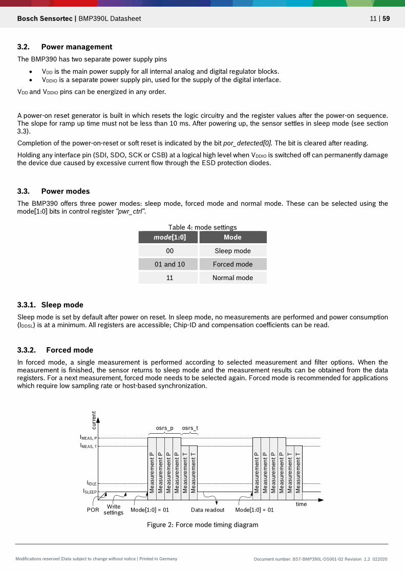
3.3.2. Forced mode In forced mode, a single measurement is performed according to selected measurement and filter options. When the measurement is finished, the sensor returns to sleep mode and the measurement results can be obtained from the data registers. For a next measurement, forced mode needs to be selected again. Forced mode is recommended for applications which require low sampling rate or host-based synchronization.
time
curre
nt
ISLEEP
IIDLE
IMEAS, P
IMEAS, T
POR Mode[1:0] = 01 Data readout
osrs_tosrs_p
Writesettings Mode[1:0] = 01
Mea
sure
men
t P
M
easu
rem
ent P
Mea
sure
men
t P
M
easu
rem
ent P
Mea
sure
men
t TM
easu
rem
ent T
Mea
sure
men
t P
M
easu
rem
ent P
Mea
sure
men
t P
M
easu
rem
ent P
Mea
sure
men
t TM
easu
rem
ent T
Figure 2: Force mode timing diagram

Bosch Sensortec | BMP390L Datasheet 12 | 59
Modifications reserved |Data subject to change without notice | Printed in Germany Document number: BST-BMP390L-DS001-02 Revision_1.2_022020
3.3.3. Normal mode Normal mode continuously cycles between an (active) measurement period and an (inactive) standby period. The measurement rate is set in the odr_sel register (see 4.3.19), where various prescaler for sample frequencies fsampling=200Hz can be selected. The sampling period 𝜏𝜏 calculated by
𝜏𝜏𝑠𝑠𝑠𝑠𝑠𝑠𝑠𝑠𝑠𝑠𝑠𝑠𝑠𝑠𝑠𝑠 = 𝑝𝑝𝑝𝑝𝑝𝑝𝑝𝑝𝑝𝑝𝑝𝑝𝑝𝑝𝑝𝑝𝑝𝑝/𝑓𝑓𝑠𝑠𝑠𝑠𝑠𝑠𝑠𝑠𝑠𝑠𝑠𝑠𝑠𝑠𝑠𝑠.
After setting the mode, measurement and filter options, the last measurement results can be obtained from the data registers without the need of further write accesses. Normal mode is recommended when using the IIR filter, and useful for applications in which short-term disturbances (e.g. blowing into the sensor) should be filtered.
time
curre
nt
ISLEEP
IIDLE
IMEAS, P
IMEAS, T
POR Mode[1:0] = 11 Data readout when needed
Writesettings
τsampling
Mea
sure
men
t P
M
easu
rem
ent P
Mea
sure
men
t P
M
easu
rem
ent P
Mea
sure
men
t TM
easu
rem
ent T
osrs_tosrs_pM
easu
rem
ent P
Mea
sure
men
t P
M
easu
rem
ent P
Mea
sure
men
t P
M
easu
rem
ent T
Mea
sure
men
t T
Figure 3: Normal mode timing diagram

Bosch Sensortec | BMP390L Datasheet 13 | 59
Modifications reserved |Data subject to change without notice | Printed in Germany Document number: BST-BMP390L-DS001-02 Revision_1.2_022020
3.3.4. Mode transition diagram The supported mode transitions are displayed below. If the device is currently performing a measurement, execution of mode switching commands is delayed until the end of the currently running measurement period. Further mode change commands are ignored until the last mode change command is executed. Also, mode change commands that are not legal are ignored.
Power OFF(VDDA or VDDD = 0)
VDDA and VDDD supplied
Sleep
Normal(cyclic standby and
measurement periods)
Forced(one measurement
period)
Figure 4: Mode transition diagram
3.4. Measurement flow The BMP390 measurement period consists of a temperature and pressure measurement with selectable oversampling. After the measurement period, the data are passed through an optional IIR filter, which removes short-term fluctuations in pressure (e.g. caused by slamming a door). The flow is depicted in the diagram below.
Figure 5: BMP390 measurement cycle
The individual blocks of the diagram above will be detailed in the following subsections.
Measure pressure (oversampling set by osrs_p;
skip if press_en = 0)
Startmeasurement cycle
Measure temperature (oversampling set by osrs_t;
skip if temp_en = 0)
IIR filter enabled?
End measurement cycle
IIR filter initialised?Copy ADC valuesto filter memory
(initalises IIR filter)No
Update filter memory using filter memory, ADC value
and filter coefficient
No
Yes
Yes
Copy filter memory to output registers,
send filter memory to FIFO

Bosch Sensortec | BMP390L Datasheet 14 | 59
Modifications reserved |Data subject to change without notice | Printed in Germany Document number: BST-BMP390L-DS001-02 Revision_1.2_022020
3.4.1. Pressure measurement Pressure measurement can be enabled or skipped. Skipping the measurement could be useful if BMP390 is used as temperature sensor. When enabled, several oversampling options exist. Each oversampling step reduces noise and increases the output resolution by one bit, which is stored in the XLSB data register. Enabling the measurement is selected by press_en bit in “PW_CTRL[0]” register (see 4.3.17). The oversampling setting osr_p can be configured in “OSR[2:0]” register (see 4.3.18).
Table 5: osr_p settings
Oversampling setting osr_p Pressure oversampling
Typical pressure resolution
Recommended temperature
oversampling
Ultra low power 000 ×1 16 bit / 2.64 Pa ×1
Low power 001 ×2 17 bit / 1.32 Pa ×1
Standard resolution 010 ×4 18 bit / 0.66 Pa ×1
High resolution 011 ×8 19 bit / 0.33 Pa ×1
Ultra high resolution 100 ×16 20 bit / 0.17 Pa ×2
Highest resolution 101 ×32 21 bit / 0.085 Pa ×2
3.4.2. Temperature measurement Temperature measurement can be enabled or skipped. Skipping the measurement could be useful to measure pressure extremely rapidly. When enabled, several oversampling options exist. Each oversampling step reduces noise and increases the output resolution by one bit, which is stored in the XLSB data register. Noise and increases the output resolution by one bit, which is stored in the XLSB data register. Enabling the measurement is selected by temp_en bit in “PW_CTRL[1]” register (see 4.3.17). The oversampling setting osr_t can be configured in “OSR[5:3]” register (see 4.3.18).
Table 6: osrs_t settings
osr_t Temperature oversampling
Typical temperature resolution
000 ×1 16 bit / 0.0050 °C
001 ×2 17 bit / 0.0025 °C
010 ×4 18 bit / 0.0012 °C
011 ×8 19 bit / 0.0006 °C
100 ×16 20 bit / 0.0003 °C
101 ×32 21 bit / 0.00015 °C
It is recommended to base the value of osr_t on the selected value of osrs_p as per Table 5. Temperature oversampling above ×2 is possible, but will not significantly improve the accuracy of the pressure output any further. The reason for this is that the noise of the compensated pressure value depends more on the raw pressure than on the raw temperature noise. Following the recommended setting will result in an optimal noise-to-power ratio.

Bosch Sensortec | BMP390L Datasheet 15 | 59
Modifications reserved |Data subject to change without notice | Printed in Germany Document number: BST-BMP390L-DS001-02 Revision_1.2_022020
3.4.3. IIR filter The environmental pressure is subject to many short-term changes, caused e.g. by slamming of a door or window, or wind blowing into the sensor. To suppress these disturbances in the output data without causing additional interface traffic and processor work load, the BMP390 features an internal IIR filter. It effectively reduces the bandwidth of the output signals9. The output of a next measurement step is filter using the following formula:
𝑑𝑑𝑝𝑝𝑑𝑑𝑝𝑝𝑓𝑓𝑠𝑠𝑠𝑠𝑓𝑓𝑓𝑓𝑓𝑓𝑓𝑓𝑓𝑓 = 𝑑𝑑𝑝𝑝𝑑𝑑𝑝𝑝𝑓𝑓𝑠𝑠𝑠𝑠𝑓𝑓𝑓𝑓𝑓𝑓𝑓𝑓𝑓𝑓_𝑜𝑜𝑠𝑠𝑓𝑓 ∗ 𝑓𝑓𝑓𝑓𝑝𝑝𝑑𝑑𝑝𝑝𝑝𝑝_𝑝𝑝𝑐𝑐𝑝𝑝𝑓𝑓𝑓𝑓𝑓𝑓𝑝𝑝𝑓𝑓𝑝𝑝𝑐𝑐𝑑𝑑 + 𝑑𝑑𝑝𝑝𝑑𝑑𝑝𝑝𝐴𝐴𝐴𝐴𝐴𝐴
𝑓𝑓𝑓𝑓𝑝𝑝𝑑𝑑𝑝𝑝𝑝𝑝_𝑝𝑝𝑐𝑐𝑝𝑝𝑓𝑓𝑓𝑓𝑓𝑓𝑝𝑝𝑓𝑓𝑝𝑝𝑐𝑐𝑑𝑑 + 1
where data_filtered_old is the data coming from the previous acquisition, and data_ADC is the data coming from the ADC before IIR filtering. The IIR filter can be configured using setting iir_filter in “CONFIG” register (see 4.3.21). When writing to the register filter, the filter is reset. The next value will pass through the filter and be the initial memory value for the filter. IIR filter is reset if the temperature or pressure measurement is disabled (temp_en or press_en registers changed from ‘1’ to ‘0’) or when a transition from sleep mode to normal mode occurs. After enabling of pressure or temperature measurement, the filtering will start, thus the next incoming value will pass unfiltered and be the initial value of the IIR filter. The step response (e.g. response to in sudden change in height) of different filter settings is displayed in Figure 6.
Figure 6: Step response at different IIR filter settings
3.4.4. Oversampling Noise depends on the oversampling and filter settings selected. The stated values were determined in a controlled pressure environment and are based on the average standard deviation of 32 consecutive measurement points taken at highest sampling rate (for details please refer to Table 22). This is required to exclude long term drifts from the noise measurement.
9 Since most pressure sensors do not sample continuously, filtering can suffer from signals with a frequency higher than the sampling rate of the sensor. E.g. environmental fluctuations caused by windows being opened and closed might have a frequency <5 Hz. Consequently, a sampling rate of ODR = 10 Hz is sufficient to obey the Nyquist theorem.

Bosch Sensortec | BMP390L Datasheet 16 | 59
Modifications reserved |Data subject to change without notice | Printed in Germany Document number: BST-BMP390L-DS001-02 Revision_1.2_022020
Table 7: Noise in pressure Typical RMS noise in pressure [Pa]
Oversampling setting
IIR filter coefficient
off 2 4 8 16 32 64 128
Ultra low power 3.7 2.0 1.2 0.8 0.4 0.2 0.1 0.1
Low power 2.7 1.5 0.9 0.5 0.3 0.2 0.1 0.1
Standard resolution 2.0 1.1 0.7 0.4 0.3 0.2 0.1 0.04
High resolution 1.6 0.9 0.6 0.3 0.2 0.1 0.1 0.03
Ultra high resolution 1.2 0.6 0.4 0.2 0.1 0.1 0.04 0.03
Highest resolution 0.9 0.5 0.3 0.2 0.1 0.1 <0.1 <0.1
Table 8: Noise in temperature Typical RMS noise in temperature [°C]
Temperature oversampling IIR filter off
Ultra low power 0.005
Low power 0.005
Standard resolution 0.005
High resolution 0.005
Ultra high resolution 0.004
Highest resolution 0.003

Bosch Sensortec | BMP390L Datasheet 17 | 59
Modifications reserved |Data subject to change without notice | Printed in Germany Document number: BST-BMP390L-DS001-02 Revision_1.2_022020
3.5. Filter selection In order to select optimal settings, the following use cases are suggested:
Table 9: Recommended filter settings based on use cases
Use case Mode Over-
sampling setting
osrs_p osrs_t
IIR filter coeff. (see
4.3.21)
IDD [µA] (see 3.8)
ODR [Hz] (see 3.4.1)
RMS Noise [cm]
(see 3.4.4)
handheld device low-
power (e.g.
Android)
Normal High resolution x8 ×1 2 145 12.5 11
handheld device
dynamic (e.g.
Android)
Normal Standard resolution ×4 ×1 4 310 50 10
Weather monitoring
(lowest power),
Forced Ultra low power ×1 ×1 Off 4 1/60 55
Drop detection Normal Low power ×2 ×1 Off 358 100 36
Indoor navigation Normal Ultra high
resolution ×16 ×2 4 560 25 5
Drone Normal Standard Resolution x8 x1 2 570 50 11

Bosch Sensortec | BMP390L Datasheet 18 | 59
Modifications reserved |Data subject to change without notice | Printed in Germany Document number: BST-BMP390L-DS001-02 Revision_1.2_022020
3.6. FIFO Description The BMP390 contains a 512 Bytes FIFO (first-in-first-out) data buffer. To enable data collecting in the FIFO, fifo_mode is set at ‘1’ and data to be collected are defined through fifo_press_en and fifo_temp_en. The FIFO mode is disabled, when no writing is defined which according to the following two cases:
• fifo_mode=’0’ • fifo_mode=’1’ and fifo_press_en=’0’ and fifo_temp_en=’0’
If the FIFO is disabled when FIFO byte count is greater than 0, no new frame is written to the FIFO, but FIFO is operational:
• Frames already written in the FIFO remain stored and can be read out • FIFO interrupts and their corresponding statuses are still evaluated • after all bytes are read out, Sensortime (if enabled) and Empty frames are generated • FIFO can be flushed
3.6.1. FIFO input data Storing of pressure and/or temperature measurement results is enabled by setting fifo_press_en=’1’ and fifo_temp_en=’1’ respectively. Storing of data can be enabled or disabled on a per-channel basis in any combination. Filtered or unfiltered data are stored to the FIFO; if data_select=”01”, filtered data are stored, otherwise unfiltered data are stored to the FIFO. The Number of bytes available in FIFO is readable through fifo_length_1<0> (MSBs) and fifo_length_0<7:0> (LSBs) registers. The FIFO byte count registers fifo_length_0 and fifo_length_1 are updated only when a full frame has been written to FIFO and is available for read-out. FIFO byte count registers are also updated after each full-frame read from the FIFO. FIFO byte count registers increment or decrement is equal to frame length; intermediate increments (corresponding to a partial frame) are not readable.
3.6.2. FIFO data sampling selection The FIFO input data rate is reduced by selecting a down-sampling factor in register fifo_subsampling. Down-sampling factor ranges from 1 to 128 and is equal to 2fifo_subsampling. Down-sampling is applied in the normal mode only and is aligned to the measurement timing grid. Down-sampling counter is reset and data saved to the FIFO at the end of the first measurement when a transition from sleep mode to normal mode occurs.
3.6.3. FIFO read out FIFO is read out via fifo_data register. FIFO reads are never blocked, however an ongoing read from the FIFO does not block writing to the FIFO. During burst read, the address counter stops incrementing when fifo_data address is reached; this allows a complete reading of the FIFO content within one burst read transaction.

Bosch Sensortec | BMP390L Datasheet 19 | 59
Modifications reserved |Data subject to change without notice | Printed in Germany Document number: BST-BMP390L-DS001-02 Revision_1.2_022020
3.6.4. FIFO overflow behavior A FIFO overflow occurs if the FIFO is full and a new data is written to the FIFO. FIFO full means free space is less than maximum frame length (9 bytes). In case of overflow the FIFO can either stop recording data or overwrite the oldest data. The behavior is controlled by register fifo_stop_on_full.
• Streaming mode, fifo_stop_on_full=’0’: if the new frame does not fit inside the remaining free space in the FIFO RAM, FIFO will repeatedly delete the oldest frame until it creates enough space for the new one.
• FIFO stop-on-full mode, fifo_stop_on_full=’1’: The newest frame is discarded. Normal operation resumes if the FIFO full condition no longer persists.
3.6.5. FIFO Frames One data frame is composed of a header and a set of data organize as described in table below.
Table 10: Data frame composition Bit 7 6 5 4 3 2 1 0
Header fh_mode[1:0] fh_param[3:0] 0 0
Data Data bytes
The number of data bytes is defined by the header.
3.6.5.1. Header Format
Table 11: Header format fh_mode[1:0] Definition fh_param[3:0]
10 Sensor frame Sensor enable bits
01 Control frame: configuration error 0001
01 Control frame: FIFO input configuration change 0010
3.6.5.2. Sensor Frame Format A sensor frame consists of a header and data bytes
Table 12: Sensor frame format Bit 7 6 5 4 3 2 1 0
Header 1 0 s t 0 p 0 0
Data data bytes
Sensor data in frame is defined by s (time), t (temperature) and p (pressure) sensor enable bits:
• If s=’1’, the frame corresponds to the sensor-time frame, in that case, t=p=’0’ • If t=’1’ or/and p=’1’, the frame corresponds to a normal pressure or/and a temperature frame • If s=t=p=’0’, the frame corresponds to an empty frame

Bosch Sensortec | BMP390L Datasheet 20 | 59
Modifications reserved |Data subject to change without notice | Printed in Germany Document number: BST-BMP390L-DS001-02 Revision_1.2_022020
Table 13: Sensor-time frame Bit 7 6 5 4 3 2 1 0
Header 1 0 1 0 0 0 0 0
Sensor-time
time_xlsb[7:0]
time_lsb[7:0]
time_msb[7:0]
The data for the sensor-time frame consists of register sensor_time content at the time the sensortime frame transmission has started. A sensor-time frame is not stored in the FIFO, but append to every FIFO burst read operation after all data has been transmitted if fifo_time_en=‘1’.
Table 14: Normal pressure and temperature frame Bit 7 6 5 4 3 2 1 0
Header 1 0 0 1 0 1 0 0
Temp temp_xlsb[7:0]
temp_lsb[7:0]
temp_msb[7:0]
Press press_xlsb[7:0]
press_lsb[7:0]
press_msb[7:0]
If one of t and p is ‘0’, the corresponding data is not part of the frame; the frame is therefore reduced to 4 bytes. A FIFO empty frame is a sensor frame with no sensor enabled. This frame is returned if the last frames was read-out or if FIFO is empty.
Table 15: FIFO empty frame format Bit 7 6 5 4 3 2 1 0
Header 1 0 0 0 0 0 0 0
Data 0 0 0 0 0 0 0 0
When a configuration error is detected, a configuration error frame is stored into the FIFO
Table 16: Control frame: FIFO input configuration
Bit 7 6 5 4 3 2 1 0
Header 0 1 0 0 1 0 0 0
Opcode 0 0 0 0 0 0 0 1

Bosch Sensortec | BMP390L Datasheet 21 | 59
Modifications reserved |Data subject to change without notice | Printed in Germany Document number: BST-BMP390L-DS001-02 Revision_1.2_022020
Table 17: Control frame: configuration error Bit 7 6 5 4 3 2 1 0
Header 0 1 0 0 0 1 0 0
Opcode 0 0 0 0 0 0 0 1
If FIFO is enabled and a change in registers “FIFO_CONF_2” or “OSR” or “ODR” or “CONFIG” or press_en or temp_en occurs, a control frame is inserted just before the first sensor frame with new configuration is stored to the FIFO. If multiple configuration change becomes active at the same time, only one control frame is inserted. Configuration changes are tracked when the device is in normal mode.
3.6.6. Corner cases 3.6.6.1. Under-read In case the FIFO is under-read (not all frames were taken from the FIFO, but the last frame read was read entirely), the next readout will continue at the frame that was just about to be sent.
3.6.6.2. Partial frame read In case the FIFO is under-read and a partial data frame read occurred (not all frames were taken from the FIFO, and the last frame read was not read entirely), the entire last data frame is repeated upon the next read access. When fifo_stop_on_full=’0’, the oldest frames are overwritten when new frames are available and the FIFO is full. When this happens, the partially read data frame is not repeated but the oldest frame available in the RAM is sent instead. Sensortime frame is not repeated when read only partially, its payload always contains current sensortime counter value. If the read of the frame is interrupted after two or more bits of the frame’s last byte were already read, then frame is discarded even though not all bits were read and the frame was read only partially.
3.6.6.3. Over-read If the burst read continues after all frames have been read out, a sensortime frame is sent after the FIFO becomes empty during a burst read operation if fifo_time_en=’1’. After that or when FIFO was completely read, the empty frame is returned as long as the burst read is active.
3.6.7. FIFO flush conditions The FIFO can be flushed by issuing either fifo_flush or a softreset in the command register “CMD” (see 4.3.23):
Table 18: fifo_fluch and softreset commands Value
fifo_flush 0xB0
softreset 0xB6

Bosch Sensortec | BMP390L Datasheet 22 | 59
Modifications reserved |Data subject to change without notice | Printed in Germany Document number: BST-BMP390L-DS001-02 Revision_1.2_022020
3.7. Interrupts The BMP390 provides an interrupt pin (INT), which allows to signal certain events to the host processor. Different events can be mapped to the interrupt pin, which all are processed with a logical OR. The available interrupts are listed below and can be read in the “INT_STATUS” register (see 4.3.9):
• FIFO watermark interrupt • FIFO full interrupt • Data ready interrupt
3.7.1. Interrupt default mode After a power-on or soft reset has completed, the interrupt pin is in push-pull and active high mode.
3.7.2. Interrupt pin latching The chip can be operated in non-latched or latched mode:
• Non-latched mode: Interrupts’ conditions are selected as a contributors to the INT pad. INT pad is de-asserted as soon as the conditions of all the interrupts propagated to the INT pad are not valid. For data ready, interrupt contribution is de-asserted by reading int_status or after 2.5ms after assertion of the interrupt. For FIFO interrupts, INT pad contributions are not affected by fifo_data readings, only by the interrupt conditions
• Latched mode: Interrupt statuses are selected as contributors of the INT pad. The minimum interrupt pulse width is Tint = 1µs
3.7.3. Monitoring The status of interrupt bits is always visible in the “INT_STATUS” register. (see 4.3.9) for details.
3.7.4. Interrupt Pin Configuration The interrupt pin / pad is configured by the Bits in the “INT_CTRL” register (see 4.3.15). However, the status bits are not influenced thereby. The output mode of the INT pad is controlled by int_od bit:
Table 19: int_od int_od=’0’ Push-pull
int_od=’1’ Open-drain
The level of the interrupt pad can be configured and switched by int_level between active low and active high:
Table 20: int_level int_level=’0’ active_low
int_level=’1’ active_high
The latching of interrupts for INT pad and INT_STATUS register can be enabled by int_latch=’1’ or disabled by int_latch=’0’.

Bosch Sensortec | BMP390L Datasheet 23 | 59
Modifications reserved |Data subject to change without notice | Printed in Germany Document number: BST-BMP390L-DS001-02 Revision_1.2_022020
FIFO interrupts are mapped to the INT pad by enabling the respective functions. For mapping FIFO watermark reached interrupt to the pad, the fwtm_en bit shall be written to ’1’ (disabling by ‘0’). The FIFO full interrupt can be mapped by writing ffull_en with ‘1’).
3.7.5. Interrupt functions 3.7.5.1. FIFO watermark interrupt The FIFO watermark interrupt is used to signal, that fill level of the FIFO has reached a pre-set limit.
Fifo_length_1 & fifo_length_0 ≥ fifo_wtm_1 & fifo_wtm_0 The watermark level can be set and adjusted by the user by writing the registers and 0x15 “FIFO_WTM_0” and 0x16 “FIFO_WTM_1” (see 4.3.12) in a single burst transaction. If the FIFO watermark level is set to zero, the interrupt condition will never be satisfied. The status of the watermark interrupt can be read back through the fwm_int bit. The interrupt condition is also updated after the end of a serial interface transaction which wrote into the registers fifo_wtm_0 or fifo_wtm_1.
Figure 7: FIFO watermark interrupt, non-latched with reads from FIFO
Figure 8: FIFO watermark interrupt, latched, with reads from FIFO

Bosch Sensortec | BMP390L Datasheet 24 | 59
Modifications reserved |Data subject to change without notice | Printed in Germany Document number: BST-BMP390L-DS001-02 Revision_1.2_022020
3.7.5.2. FIFO full interrupt FIFO Full interrupt status is asserted when the full interrupt condition is satisfied, when the filling level of the FIFO number of unread bytes in the FIFO = fifo_length_1 & fifo_length_0 is equal or higher than 504. The status of the FIFO full interrupt can be read back through the ffull_int bit. Interrupt status is cleared by reading the ffull_int bit high ‘1’ when the FIFO filling level is lower than 504. The FIFO full interrupt is propagated to INT pad only when it is enabled by setting bit ffull_en=‘1’. Latching mode configuration bit int_latch selects whether the interrupt status or condition is propagated to the INT pad.
Figure 9:FIFO full interrupt, non-latched, with reads from FIFO
Figure 10: FIFO full interrupt, latched, with reads from FIFO
3.7.5.3. Data ready Data ready interrupt status int_status.drdy is asserted after a pressure and temperature measurement ends and conversion results are stored to the data registers and to the FIFO. The status of the interrupt can be read back through the drdy bit. The data ready interrupt is propagated to INT pad when it is enabled by setting drdy_en=‘1’. Interrupt status is cleared by reading drdy bit high ‘1’. Data ready INT pad contribution is cleared automatically 2.5 ms after the interrupt assertion in the non-latched mode (int_latch=’0’). Corner cases:
• If data ready interrupt is changed from latched to non-latched mode (int_latched changed from ‘1’ to ‘0’) after the interrupt was already asserted; timer is not running and it is not starting during the ongoing measurement, self-clearing does not happen. Timer is starting when next data ready comes.
• If data ready is changed to be propagated to INT pad (drdy_int changed from ‘0’ to ‘1’) after the interrupt was already asserted; data ready INT pad contribution remains ‘0’ until next data ready interrupt assertion.

Bosch Sensortec | BMP390L Datasheet 25 | 59
Modifications reserved |Data subject to change without notice | Printed in Germany Document number: BST-BMP390L-DS001-02 Revision_1.2_022020
Figure 11: Data ready interrupt, non-latched mode, with read of data registers
Figure 12: Data ready interrupt, non-latched mode, with read of data registers during register update
Figure 13: Data ready interrupt, latched mode, with read of data registers

Bosch Sensortec | BMP390L Datasheet 26 | 59
Modifications reserved |Data subject to change without notice | Printed in Germany Document number: BST-BMP390L-DS001-02 Revision_1.2_022020
3.8. Current consumption
The current consumption depends on ODR and oversampling setting. The values given below are normalized to an ODR of 1 Hz. The actual consumption at a given ODR can be calculated by multiplying the consumption in Table 21 with the ODR used. The actual ODR is defined either by the frequency at which the user sets forced measurements or by oversampling and sampling period settings in normal mode in Table 24.
Table 21: Current consumption Oversampling setting Pressure
oversampling Temperature oversampling
IDD [µA] @ 1 Hz forced mode
Typ Calculated Forced Mode
Max
Ultra low power ×1 ×1 3.4 4.3 7.4
Low power ×2 ×1 4.8 5.6 9.3
Standard resolution ×4 ×1 7.8 8.2 12.8
High resolution ×8 ×1 13.8 13.3 19.5
Ultra high resolution ×16 ×2 26.2 24.3 33.5
highest resolution ×32 ×2 46.4 45.0 59.2
3.9. Measurement timings
The rate at which measurements can be performed in forced mode depends on the oversampling settings osr_t and osr_p. Thus in normal mode, the measurement rate is determined by the sampling frequency fsample.
3.9.1. Measurement time The following table explains the typical and maximum measurement time based on selected oversampling setting. The minimum achievable frequency is determined by the maximum measurement time.
Table 22: measurement time Oversampling
setting Pressure
oversampling Temperature oversampling
Measurement time[ms]
Measurement rate [Hz]
Typ Max Typ Min
Ultra low power ×1 ×1 4.82 5.70 207.08 175.39
Low power ×2 ×1 6.84 7.96 146.00 125.56
Standard resolution ×4 ×1 10.88 12.48 91.83 80.07
High resolution ×8 ×1 18.69 21.53 52.71 46.42
Ultra high resolution ×16 ×2 37.14 41.89 26.91 23.86
highest resolution ×32 ×2 69.46 78.09 14.39 12.80

Bosch Sensortec | BMP390L Datasheet 27 | 59
Modifications reserved |Data subject to change without notice | Printed in Germany Document number: BST-BMP390L-DS001-02 Revision_1.2_022020
3.9.2. Measurement rate in forced mode and normal mode In both forced mode and normal mode the pressure and temperature measurement duration follow the equation:
𝑇𝑇𝑐𝑐𝑜𝑜𝑠𝑠𝑐𝑐 = 234µ𝑝𝑝 + 𝑝𝑝𝑝𝑝𝑝𝑝𝑝𝑝𝑝𝑝_𝑝𝑝𝑐𝑐 ∙ (392µ𝑝𝑝 + 2𝑜𝑜𝑠𝑠𝑓𝑓_𝑠𝑠 ∙ 2020µ𝑝𝑝) + 𝑑𝑑𝑝𝑝𝑡𝑡𝑝𝑝_𝑝𝑝𝑐𝑐 ∙ (163µ𝑝𝑝 + 2𝑜𝑜𝑠𝑠𝑓𝑓_𝑓𝑓 ∙ 2020µ𝑝𝑝) With:
𝑇𝑇𝑐𝑐𝑜𝑜𝑠𝑠𝑐𝑐 = total conversion time in µs
𝑝𝑝𝑝𝑝𝑝𝑝𝑝𝑝𝑝𝑝_𝑝𝑝𝑐𝑐 = “0” or “1”, depending of the status of the press_en bit 𝑑𝑑𝑝𝑝𝑡𝑡𝑝𝑝_𝑝𝑝𝑐𝑐 = “0” or “1”, depending of the status of the temp_en bit
2𝑜𝑜𝑠𝑠𝑓𝑓_𝑠𝑠 = amount of pressure oversampling repetitions
2𝑜𝑜𝑠𝑠𝑓𝑓_𝑓𝑓 = amount of temperature oversampling repetitions Maximum possible readout frequency in forced mode (typical):
𝑓𝑓𝑠𝑠𝑠𝑠𝑚𝑚 =1
𝑇𝑇𝑐𝑐𝑜𝑜𝑠𝑠𝑐𝑐[µ𝑝𝑝] ∙ 106
Maximum possible readout frequency in normal mode:
𝑐𝑐𝑑𝑑𝑝𝑝_𝑝𝑝𝑝𝑝𝑝𝑝 = 𝑝𝑝𝑐𝑐𝑔𝑔2 200𝐻𝐻𝐻𝐻𝑓𝑓𝑠𝑠𝑠𝑠𝑚𝑚[𝐻𝐻𝐻𝐻]
𝑓𝑓𝑠𝑠𝑠𝑠𝑚𝑚_𝑠𝑠𝑜𝑜𝑓𝑓𝑠𝑠𝑠𝑠𝑠𝑠_𝑠𝑠𝑜𝑜𝑓𝑓𝑓𝑓 =200𝐻𝐻𝐻𝐻2𝑜𝑜𝑓𝑓𝑓𝑓_𝑠𝑠𝑓𝑓𝑠𝑠
3.10. Data readout from data registers
To read out data after a conversion, it is strongly recommended to use a burst read and not address every register individually. This will prevent a possible mix-up of bytes belonging to different measurements and reduce interface traffic. Data readout is done by starting a burst read from register press_xlsb to temp_msb. The data are read out in an unsigned 24-bit format both for pressure and for temperature. The timing for data readout in forced mode should be done so that the maximum measurement times (see Sec. 3.9.1) are respected. In normal mode, readout can be done at a speed similar to the expected data output rate (see Sec. 3.9.2). After the uncompensated values of temperature and pressure have been read, the actual pressure and temperature need to be calculated using the compensation parameters stored in the device. The procedure is elaborated in Sec. 3.11.
3.10.1. Data register shadowing In normal mode, measurement timing is not necessarily synchronized to readout. This means that new measurement results may become available while the user is reading the results from the previous measurement. In this case, shadowing is performed in order to guarantee data consistency. Shadowing will only work if all data registers are read in a single burst read. Therefore, the user must use burst reads if he does not synchronize data readout with the measurement cycle. Using several independent read commands may result in inconsistent data. If a new measurement is finished and the data registers are still being read, the new measurement results are transferred into shadow data registers. The content of shadow registers is transferred into data registers as soon as the user ends the burst read, even if not all data registers were read. Reading across several data registers can therefore only be guaranteed to be consistent within one measurement cycle if a single burst read command is used. The end of the burst read is marked by the rising edge of CSB pin. After the end of the burst read, all user data registers are updated at once.

Bosch Sensortec | BMP390L Datasheet 28 | 59
Modifications reserved |Data subject to change without notice | Printed in Germany Document number: BST-BMP390L-DS001-02 Revision_1.2_022020
3.11. Output compensation The BMP390 output consists of the ADC output values (including oversampling). However, each sensing element behaves differently, and thus in order to receive the most accurate physical values for temperature and pressure, compensation formulae have to be applied to the raw output values received from the sensor. The coefficients used for the compensation are stored into the devices’ non-volatile memory (NVM) during production (see Table 23). For the compensation formula please see Appendix 0.
3.11.1. Memory Map Trimming Coefficients
Table 23: Trimming Coefficient listing in register map with size and sign attributes Memory-
ADR_Read [dec]
Memory-ADR_Read
[hex] Register content Trimming
Coefficient Size Sign
69 0x45 NVM_PAR_P11<7:0> NVM_PAR_P11 8 Bit signed
68 0x44 NVM_PAR_P10<7:0> NVM_PAR_P10 8 Bit signed
67 0x43 NVM_PAR_P9<15:8> NVM_PAR_P9 16
Bit signed 66 0x42 NVM_PAR_P9<7:0>
65 0x41 NVM_PAR_P8<7:0> NVM_PAR_P8 8 Bit signed
64 0x40 NVM_PAR_P7<7:0> NVM_PAR_P7 8 Bit signed
63 0x3F NVM_PAR _P6<15:8> NVM_PAR _P6 16
Bit unsigned 62 0x3E NVM_PAR _P6<7:0>
61 0x3D NVM_PAR _P5<15:8> NVM_PAR _P5 16
Bit unsigned 60 0x3C NVM_PAR _P5<7:0>
59 0x3B NVM_PAR _P4<7:0> NVM_PAR _P4 8 Bit signed
58 0x3A NVM_PAR _P3<7:0> NVM_PAR _P3 8 Bit signed
57 0x39 NVM_PAR _P2<15:8> NVM_PAR _P2 16
Bit signed 56 0x38 NVM_PAR _P2<7:0>
55 0x37 NVM_PAR _P1<15:8> NVM_PAR _P1 16
Bit signed 54 0x36 NVM_PAR _P1<7:0>
53 0x35 NVM_PAR _T3<7:0> NVM_PAR _T3 8 Bit signed
52 0x34 NVM_PAR _T2<15:8> NVM_PAR _T2 16
Bit unsigned 51 0x33 NVM_PAR _T2<7:0>
50 0x32 NVM_PAR _T1<15:8> NVM_PAR _T1 16
Bit unsigned 49 0x31 NVM_PAR _T1<7:0>

Bosch Sensortec | BMP390L Datasheet 29 | 59
Modifications reserved |Data subject to change without notice | Printed in Germany Document number: BST-BMP390L-DS001-02 Revision_1.2_022020
4. Global memory map and register description
4.1. General remarks All communication with the device is performed by reading and writing registers. All Registers have a width of 8 bits. There are several registers which are reserved; they should not be written to and no specific value is guaranteed when they are read. For details on the interface, consult chapter 5.
4.2. Datasheet Memory Map The memory map is given in Table 24.

Bosch Sensortec | BMP390L Datasheet 30 | 59
Modifications reserved |Data subject to change without notice | Printed in Germany Document number: BST-BMP390L-DS001-02 Revision_1.2_022020
Table 24: BMP390 memory map
read/write read only write only reserved
Register Address Register Name Default
Value 7 6 5 4 3 2 1 0
0x7E CMD 0x00 cmd
0x7D - - reserved
... - - reserved
0x20 - - reserved
0x1F CONFIG 0x00 reserved iir_filter short_in
0x1E - - reserved
0x1D ODR 0x00 reserved odr_sel
0x1C OSR 0x02 reserved osr_t osr_p
0x1B PWR_CTRL 0x00 reserved mode reserved temp_en press_en
0x1A IF_CONF 0x00 reserved i2c_wdt_sel i2c_wdt_en spi3
0x19 INT_CTRL 0x02 reserved drdy_en int_ds ffull_en fwtm_en int_latch int_level int_od
0x18 FIFO_CONFIG_2 0x02 reserved data_select fifo_subsampling
0x17 FIFO_CONFIG_1 0x02 reserved fifo_temp_en fifo_press_en fifo_time_en fifo_stop_on_full fifo_mode
0x16 FIFO_WTM_1 0x00 reserved fifo_water_mark_8
0x15 FIFO_WTM_0 0x01 fifo_water_mark_7_0
0x14 FIFO_DATA 0x00 fifo_data
0x13 FIFO_LENGTH_1 0x00 fifo_byte_counter_11_8
0x12 FIFO_LENGTH_0 0x00 fifo_byte_counter_7_0
0x11 INT_STATUS 0x00 reserved drdy reserved ffull_int fwm_int
0x10 EVENT 0x01 reserved itf_act_pt por_detected
0x0F - - reserved
0x0E SENSORTIME_2 0x00 sensor_time_23_16
0x0D SENSORTIME_1 0x00 sensor_time_15_8
0x0C SENSORTIME_0 0x00 sensor_time_7_0
0x0B - - reserved
0x0A - - reserved
0x09 DATA_5 0x80 temp_23_16
0x08 DATA_4 0x00 temp_15_8
0x07 DATA_3 0x00 temp_7_0
0x06 DATA_2 0x80 press_23_16
0x05 DATA_1 0x00 press_15_8
0x04 DATA_0 0x00 press_7_0
0x03 STATUS 0x00 reserved drdy_temp drdy_press cmd_rdy reserved
0x02 ERR_REG 0x00 reserved conf_err cmd_err fatal_err
0x01 REV_ID 0x01 rev_id_major rev_id_minor
0x00 CHIP_ID 0x60 chip_id_fixed chip_id_nvm

Bosch Sensortec | BMP390L Datasheet 31 | 59
Modifications reserved |Data subject to change without notice | Printed in Germany Document number: BST-BMP390L-DS001-02 Revision_1.2_022020
4.3. Register description 4.3.1. Register 0x00 “CHIP_ID” The “CHIP_ID” register contains the chip identification code.
Table 25: Register 0x00 “CHIP_ID” Name Description
Bit 7..0 Chip id.
4.3.2. Register 0x01 “REV_ID” The “Rev_ID” register contains the mask revision of the ASIC
Table 26: Register 0x01 “REV_ID” Name Description
Bit 7..0 Rev id.
4.3.3. Register 0x02 “ERR_REG” Sensor Error conditions are reported in the “ERR_REG” register.
Table 27: Register 0x02 “ERR_REG” Name Description
Bit 0 fatal_err Fatal error
Bit 1 cmd_err Command execution failed. Cleared on read.
Bit 2 conf_err sensor configuration error detected (only working in normal mode). Cleared on read.

Bosch Sensortec | BMP390L Datasheet 32 | 59
Modifications reserved |Data subject to change without notice | Printed in Germany Document number: BST-BMP390L-DS001-02 Revision_1.2_022020
4.3.4. Register 0x03 “STATUS” The Sensor Status Flags are stored in the “STATUS” register.
Table 28: Register 0x03 “STATUS” Name Description
Bit 4 cmd_rdy CMD decoder status.
0: Command in progress 1: Command decoder is ready to accept a new command
Bit 5 drdy_press Data ready for pressure.
It gets reset, when one pressure DATA register is read out
Bit 6 drdy_temp Data ready for temperature sensor.
It gets reset, when one temperature DATA register is read out
4.3.5. Register 0x04 .. 0x06 Pressure Data The 24Bit pressure data is split and stored in three consecutive registers
• 0x04 “DATA_0” • 0x05 “DATA_1” • 0x06 “DATA_2”
Table 29: Pressure Data Registers Register 0x06 DATA_2 0x05 DATA_1 0x04 DATA_0
Bit 7..0 7..0 7..0
name PRESS_MSB_23_16 PRESS_LSB_15_8 PRESS_XLSB_7_0
Data pressure data
4.3.6. Register 0x07 .. 0x09 Temperature Data The 24Bit temperature data is split and stored in three consecutive registers
• 0x07 “DATA_3” • 0x08 “DATA_4” • 0x09 “DATA_5”
Table 30: Temperature Data Registers Register 0x09 DATA_5 0x08 DATA_4 0x07 DATA_3
Bit 7..0 7..0 7..0
name TEMP_MSB_23_16 TEMP_LSB_15_8 TEMP_XLSB_7_0
Data temperature data

Bosch Sensortec | BMP390L Datasheet 33 | 59
Modifications reserved |Data subject to change without notice | Printed in Germany Document number: BST-BMP390L-DS001-02 Revision_1.2_022020
4.3.7. Register 0x0C .. 0x0E Sensor Time The 24Bit sensor time is split and stored in three consecutive registers
• 0x0C “SENSORTIME_0” • 0x0D “SENSORTIME_1” • 0x0E “SENSORTIME_2”
Table 31: Sensor Time Registers Register 0x0E SENSORTIME_2 0x0D SENSORTIME_1 0x0C SENSORTIME_0
Bit 7..0 7..0 7..0
name sensor_time_23_16 sensor_time_15_8 sensor_time_7_0
Data Sensor time
4.3.8. Register 0x10 “EVENT” The “EVENT” register contains the sensor status flags.
Table 32: Register 0x10 “EVENT” Name Description
Bit 0 por_detected ‘1’ after device power up or softreset. Clear-on-read
Bit 1 itf_act_pt ‘1’ when a serial interface transaction occurs during a pressure or temperature conversion. Clear-on-read
4.3.9. Register 0x11 “INT_STATUS” The “INT_STATUS” register shows interrupt status and is cleared after reading.
Table 33: Register 0x11 “INT_STATUS” Name Description
Bit 0 fwm_int FIFO Watermark Interrupt
Bit 1 ffull_int FIFO Full Interrupt
Bit 3 drdy data ready interrupt
4.3.10. Register 0x12 .. 0x13 “FIFO_LENGTH” The FIFO byte counter indicates the current fill level of the FIFO buffer. Its size is 9 bit for 512 bytes and therefore split in two registers “FIFO_LENGTH_0” and “FIFO_LENGTH_1”.
Table 34: FIFO Length Split Register 0x13 FIFO_LENGTH_1 0x12 FIFO_LENGTH_0
Bit 7 6 5 4 3 2 1 0 7 6 5 4 3 2 1 0
name fifo_byte_counter_11_8 fifo_byte_counter_7_0

Bosch Sensortec | BMP390L Datasheet 34 | 59
Modifications reserved |Data subject to change without notice | Printed in Germany Document number: BST-BMP390L-DS001-02 Revision_1.2_022020
4.3.11. Register 0x14 “FIFO_DATA” The “FIFO_DATA” is the data output register.
Table 35: Register 0x14 “FIFO_DATA” Name Description
Bit 7..0 fifo_data FIFO read data.
4.3.12. Register 0x15 .. 0x16 FIFO Watermark The FIFO Watermark size is 9 Bit and therefore written to the FIFO_WTM_0 and FIFO_WTM_1 registers.
Table 36: FIFO Watermark Register Overview Register 0x16 FIFO_WTM_1 0x15 FIFO_WTM_0
Bit 7 6 5 4 3 2 1 0 7 6 5 4 3 2 1 0
name fifo_water_mark_8 fifo_water_mark_7_0
4.3.13. Register 0x17 “FIFO_CONFIG_1” The “FIFO_CONFIG_1” register contains the FIFO frame content configuration.
Table 37: Register 0x17 “FIFO_CONFIG_1” Name Description
Bit 0 fifo_mode Enables or disables the FIFO 0 disable 1 enable FIFO mode
Bit 1 fifo_stop_on_full Stop writing samples into FIFO when FIFO is full. 0 disable do not stop writing to FIFO when full 1 enable Stop writing into FIFO when full.
Bit 2 fifo_time_en Return sensortime frame after the last valid data frame. 0 disable do not return sensortime frame 1 enable return sensortime frame
Bit 3 fifo_press_en Store pressure data in FIFO 0 disable no pressure data is stored 1 enable pressure data is stored
Bit 4 fifo_temp_en Store temperature data in FIFO 0 disable no temperature data is stored 1 enable temperature data is stored

Bosch Sensortec | BMP390L Datasheet 35 | 59
Modifications reserved |Data subject to change without notice | Printed in Germany Document number: BST-BMP390L-DS001-02 Revision_1.2_022020
4.3.14. Register 0x18 “FIFO_CONFIG_2” The “FIFO_CONFIG_2” register extends the FIFO_CONFIG_1 register.
Table 38: Register 0x18 “FIFO_CONFIG_2” Name Description
Bit 2..0 fifo_subsampling FIFO downsampling selection for pressure and temperature data, factor is
2^fifo_subsampling
Bit 4..3 data_select
for pressure and temperature, select data source 0 unfiltered data (compensated or uncompensated) 1 filtered data (compensated or uncompensated) 11/10 reserved, same as for “unfilt”
4.3.15. Register 0x19 “INT_CTRL” Interrupt configuration can be set in the “INT_CTRL” register. It affects INT_STATUS registers and the INT pin.
Table 39: Register 0x19 “INT_CTRL”
Name Description
Bit 0 int_od Configure output: open-drain or push-pull 0 push-pull 1 open-drain
Bit 1 int_level level of INT pin 0 active_low 1 active_high
Bit 2 int_latch Latching of interrupts for INT pin and INT_STATUS register 0 disabled 1 enabled
Bit 3 fwtm_en enable FIFO watermark reached interrupt for INT pin and INT_STATUS. 0 disabled 1 enabled
Bit 4 ffull_en enable Fifo full interrupt for INT pin and INT_STATUS 0 disabled 1 enabled
Bit 5 int_ds 0 low 1 high
Bit 6 drdy_en enable temperature / pressure data ready interrupt for INT pin and INT_STATUS 0 disabled 1 enabled

Bosch Sensortec | BMP390L Datasheet 36 | 59
Modifications reserved |Data subject to change without notice | Printed in Germany Document number: BST-BMP390L-DS001-02 Revision_1.2_022020

Bosch Sensortec | BMP390L Datasheet 37 | 59
Modifications reserved |Data subject to change without notice | Printed in Germany Document number: BST-BMP390L-DS001-02 Revision_1.2_022020
4.3.16. Register 0x1A “IF_CONF” The “IF_CONF” register controls the serial interface settings.
Table 40: Register 0x1A “IF_CONF” Name Description
Bit 0 spi3 Configure SPI Interface Mode for primary interface 0 spi4 SPI 4-wire mode 1 spi3 SPI 3-wire mode
Bit 1 i2c_wdt_en Enable for the I2C Watchdog timer, backed by NVM 0 disabled Watchdog disabled 1 enabled Watchdog enabled
Bit 2 i2c_wdt_sel Select timer period for I2C Watchdog , backed by NVM 0 wdt_short I2C watchdog timeout after 1.25 ms 1 wdt_long I2C watchdog timeout after 40 ms
4.3.17. Register 0x1B “PWR_CTRL” The “PWR_CTRL” register enables or disables pressure and temperature measurement. Although, the measurement mode can be set here.
Table 41: Register 0x1B “PWR_CTRL” Name Description
Bit 0 press_en 0 press_off Disables the pressure sensor. 1 press_on Enables the pressure sensor.
Bit 1 temp_en
0 temp_off Disables the temperature sensor. 1 temp_on Enables the temperature sensor.
Bit 5..4 mode
00 sleep mode 01/10 forced mode 11 normal mode

Bosch Sensortec | BMP390L Datasheet 38 | 59
Modifications reserved |Data subject to change without notice | Printed in Germany Document number: BST-BMP390L-DS001-02 Revision_1.2_022020
4.3.18. Register 0x1C “OSR” The “OSR” register controls the oversampling settings for pressure and temperature measurements.
Table 42: Register 0x1C “OSR”
4.3.19. Register 0x1D “ODR” The “ODR” register set the configuration of the output data rates by means of setting the subdivision/subsampling.
Table 43: Register 0x1D “ODR”
Name Description
Bit 2..0 osr_p Oversampling setting pressure measurement 000 x1 no oversampling. 001 x2 x2 oversampling. 010 x4 x4 oversampling. 011 x8 x8 oversampling. 100 x16 x16 oversampling. 101 x32 x32 oversampling.
Bit 5..3 osr4_t Oversampling setting temperature measurement 000 x1 no oversampling 001 x2 x2 oversampling 010 x4 x4 oversampling 011 x8 x8 oversampling 100 x16 x16 oversampling 101 x32 x32 oversampling
Name Description
Bit 4..0 odr_sel subdivision factor for pressure and temperature measurements is 2^value. Allowed values are 0..17. Other values are saturated at 17.

Bosch Sensortec | BMP390L Datasheet 39 | 59
Modifications reserved |Data subject to change without notice | Printed in Germany Document number: BST-BMP390L-DS001-02 Revision_1.2_022020
4.3.20. Control settings for odr_sel
Table 44: Control settings for odr_sel odr_sel prescaler Name Description Sampling Period
0x00 1 ODR_200 ODR 200Hz 5 ms
0x01 2 ODR_100 ODR 100Hz 10 ms
0x02 4 ODR_50 ODR 50Hz 20 ms
0x03 8 ODR_25 ODR 25Hz 40 ms
0x04 16 ODR_12p5 ODR 25/2Hz 80 ms
0x05 32 ODR_6p25 ODR 25/4Hz 160 ms
0x06 64 ODR_3p1 ODR 25/8Hz 320 ms
0x07 127 ODR_1p5 ODR 25/16Hz 640 ms
0x08 256 ODR_0p78 ODR 25/32Hz 1.280 s
0x09 512 ODR_0p39 ODR 25/64Hz 2.560 s
0x0A 1024 ODR_0p2 ODR 25/128Hz 5.120 s
0x0B 2048 ODR_0p1 ODR 25/256Hz 10.24 s
0x0C 4096 ODR_0p05 ODR 25/512Hz 20.48 s
0x0D 8192 ODR_0p02 ODR 25/1024Hz 40.96 s
0x0E 16384 ODR_0p01 ODR 25/2048Hz 81.92 s
0x0F 32768 ODR_0p006 ODR 25/4096Hz 163.84 s
0x10 65536 ODR_0p003 ODR 25/8192Hz 327.68 s
0x11 131072 ODR_0p0015 ODR 25/16384Hz 655.36 s

Bosch Sensortec | BMP390L Datasheet 40 | 59
Modifications reserved |Data subject to change without notice | Printed in Germany Document number: BST-BMP390L-DS001-02 Revision_1.2_022020
4.3.21. Register 0x1F “CONFIG” The “CONFIG” register controls the IIR filter coefficients.
Table 45: Register 0x1F “CONFIG” Name Description
Bit 3..1 iir_filter
filter coefficient for IIR filter 000 coef_0 filter coefficient is 0 -> bypass-mode 001 coef_1 filter coefficient is 1 010 coef_3 filter coefficient is 3 011 coef_7 filter coefficient is 7 100 coef_15 filter coefficient is 15 101 coef_31 filter coefficient is 31 110 coef_63 filter coefficient is 63 111 coef_127 filter coefficient is 127
4.3.22. Register 0x30 .. 0x57 “calibration data” The overview over the calibration data can be found in Chapter 3.11.1.
4.3.23. Register 0x7E “CMD” The available commands of the “CMD” register are listed below.
Table 46: Register 0x7E “CMD” Name Description
Bit 7..0 cmd All Available commands
(Note: Register will always read as 0x00)
Table 47: available cmd commands listed below Value Name Description
0x00 nop reserved. No command.
0xB0 fifo_flush Clears all data in the FIFO, does not change FIFO_CONFIG registers
0xB6 softreset Triggers a reset, all user configuration settings are overwritten with their default state

Bosch Sensortec | BMP390L Datasheet 41 | 59
Modifications reserved |Data subject to change without notice | Printed in Germany Document number: BST-BMP390L-DS001-02 Revision_1.2_022020
5. Digital interfaces The BMP390 supports the I²C and SPI digital interfaces; it acts as a slave for both protocols. The I²C interface supports the standard, fast and high speed modes. The SPI interface supports both SPI mode ‘00’ (CPOL = CPHA = ‘0’) and mode ‘11’ (CPOL = CPHA = ‘1’) in 4-wire and 3-wire configuration. The following transactions are supported:
• Single byte write • Multiple byte write (using pairs of register addresses and register data) • Single byte read • Multiple byte read (using a single register address which is auto-incremented)
5.1. Interface selection Interface selection is done automatically based on CSB (chip select) status. If CSB is connected to VDDIO, the I²C interface is active. If CSB is pulled down, the SPI interface is activated. After CSB has been pulled down once (regardless of whether any clock cycle occurred), the I²C interface is disabled until the next power-on-reset. This is done in order to avoid inadvertently decoding SPI traffic to another slave as I²C data. Since power-on-reset is only executed when both VDD and VDDIO are established, there is no risk of incorrect protocol detection due to power-up sequence used. However, if I²C is to be used and CSB is not directly connected to VDDIO but rather through a programmable pin, it must be ensured that this pin already outputs the VDDIO level during power-on-reset of the device. If this is not the case, the device will be locked in SPI mode and not respond to I²C commands.
5.2. I²C Interface The I²C slave interface is compatible with Philips I²C Specification Revision 6 (April 2014). For detailed timings refer to Table 49. All modes (standard, fast, high speed) are supported. SDA and SCL are not pure open-drain. Both pads contain ESD protection diodes to VDDIO and GND.
Figure 14: SDI/SCK ESD drawing
The 7-bit device address is 111011x. The 6 MSB bits are fixed. The last bit is changeable by SDO value and can be changed during operation. Connecting SDO to GND results in slave address 1110110 (0x76); connection it to VDDIO results in slave address 1110111 (0x77), which is the same as BMP180’s I²C address. The SDO pin cannot be left floating; if left floating, the I²C address will be undefined.

Bosch Sensortec | BMP390L Datasheet 42 | 59
Modifications reserved |Data subject to change without notice | Printed in Germany Document number: BST-BMP390L-DS001-02 Revision_1.2_022020
The I²C interface uses the following pins:
• SCK: serial clock (SCL) • SDI: data (SDA) • SDO: Slave address LSB (GND = ‘0’, VDDIO = ‘1’)
The CSB is not used and is left open. SDI is bi-directional with open drain to VSS: it must be externally connected to VDDIO via a pull up resistor. Refer to chapter 6 for connection instructions. The following abbreviations will be used in the I²C protocol figures:
• S Start • P Stop • ACKS Acknowledge by slave • ACKM Acknowledge by master • NACKM Not acknowledge by master
5.2.1. I²C write Writing is done by sending the slave address in write mode (RW = ‘0’), resulting in slave address 111011X0 (‘X’ is determined by state of SDO pin. Then the master sends pairs of register addresses and register data. The transaction is ended by a stop condition. This is depicted in Figure 15.
Figure 15: I²C write
5.2.2. I²C read To be able to read registers, first the register address must be sent in write mode (slave address 111011X0). Then either a stop or a repeated start condition must be generated. After this the slave is addressed in read mode (RW = ‘1’) at address 111011X1, after which the slave sends out data from auto-incremented register addresses until a NOACKM and stop condition occurs. This is depicted in Figure 16, where two bytes are read from register 0xF6 and 0xF7.
Figure 16: I²C multiple byte read

Bosch Sensortec | BMP390L Datasheet 43 | 59
Modifications reserved |Data subject to change without notice | Printed in Germany Document number: BST-BMP390L-DS001-02 Revision_1.2_022020
5.3. SPI interface The SPI interface is compatible with SPI mode ‘00’ (CPOL = CPHA = ‘0’) and mode ‘11’ (CPOL = CPHA = ‘1’). The automatic selection between mode ‘00’ and ‘11’ is determined by the value of SCK after the CSB falling edge. The SPI interface has two modes: 4-wire and 3-wire. The protocol is the same for both. The 3-wire mode is selected by setting spi3=‘1’ in register “IF_CONF[0]” (see 4.3.14). The pad SDI is used as a data input/output pad in 3-wire mode. The SPI interface uses the following pins:
• CSB: chip select, active low • SCK: serial clock • SDI: serial data input; data input/output in 3-wire mode • SDO: serial data output; hi-Z in 3-wire mode
Refer to chapter 6 for connection instructions. CSB is active low and has an integrated pull-up resistor. Data on SDI is latched by the device at SCK rising edge and SDO is changed at SCK falling edge. Communication starts when CSB goes to low and stops when CSB goes to high; during these transitions on CSB, SCK must be stable. The SPI protocol is shown in Figure 17.
CSB
SCK
SDI
RW AD6 AD5 AD4 AD3 AD2 AD1 AD0 DI5 DI4 DI3 DI2 DI1 DI0 DI7 DI6
SDO
DO5 DO4 DO3 DO2 DO1 DO0 DO7 DO6 tri-state Figure 17: SPI protocol (shown for mode ‘11’ in 4-wire configuration)
In SPI mode, only 7 bits of the register addresses are used; the MSB of register address is not used and replaced by a read/write bit (RW = ‘0’ for write and RW = ‘1’ for read). Example: address 0xF7 is accessed by using SPI register address 0x77. For write access, the byte 0x77 is transferred, for read access, the byte 0xF7 is transferred.
5.3.1. SPI write Writing is done by lowering CSB and sending pairs control bytes and register data. The control bytes consist of the SPI register address (= full register address without bit 7) and the write command (bit7 = RW = ‘0’). Several pairs can be written without raising CSB. The transaction is ended by a raising CSB. The SPI write protocol is depicted in Figure 18.
Figure 18: 4 wire SPI sequence
Figure 19: SPI multiple write

Bosch Sensortec | BMP390L Datasheet 44 | 59
Modifications reserved |Data subject to change without notice | Printed in Germany Document number: BST-BMP390L-DS001-02 Revision_1.2_022020
5.3.2. SPI read Reading is done by lowering CSB and first sending one control byte. The control bytes consist of the SPI register address (= full register address without bit 7) and the read command (bit 7 = RW = ‘1’). After writing the control byte, one dummy byte is sent and there after data bytes. The register address is automatically incremented. The SPI read protocol is shown in Figure 20.
Figure 20: SPI multiple byte read
5.4. Interface parameter specification 5.4.1. General interface parameters The general interface parameters are given in the table below:
Table 48: interface parameters
5.4.2. I²C timings For I²C timings, the following abbreviations are used:
• “S&F mode” = standard and fast mode • “HS mode” = high speed mode • Cb = bus capacitance on SDA line
All other naming refers to I²C specification 2.1 (January 2000). The I²C timing diagram is shown in Figure 21. The corresponding values are given in Table 49.
Parameter Symbol Condition Min Typ Max Units
Input – low level Vil SCK, SDI and CSB 0.25 VDDIO
V
Input – high level Vih SCK, SDI and CSB 0.7
VDDIO V
Output – low level Vol SDI, SDO and INT,
iol=3 mA
0.2 VDDIO
V
Output – high level Voh SDI, SDO and INT
ioh=1 mA 0.8
VDDIO V
CSB Pull-up resistor Rcsb Internal pull-up resistance to VDDIO 75 100 125 kΩ
I2C bus load capacitor Cb On SDI and SCK 400 pF
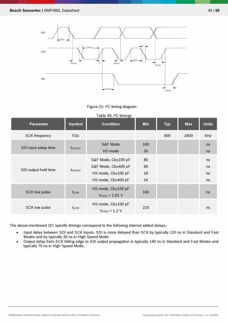
Bosch Sensortec | BMP390L Datasheet 45 | 59
Modifications reserved |Data subject to change without notice | Printed in Germany Document number: BST-BMP390L-DS001-02 Revision_1.2_022020
tHDDAT
tf
tBUF
SDI
SCK
SDI
tLOW
tHDSTA tr
tSUSTA
tHIGH
tSUDAT
tSUSTO
Figure 21: I²C timing diagram
Table 49: I²C timings
Parameter Symbol Condition Min Typ Max Units
SCK frequency Fi2c 400 3400 kHz
SDI input setup time tSU;DAT S&F Mode HS mode
160 30
ns ns
SDI output hold time tHD;DAT
S&F Mode, Cb≤100 pF S&F Mode, Cb≤400 pF HS mode, Cb≤100 pF HS mode, Cb≤400 pF
80 90 18 24
ns ns ns ns
SCK low pulse tLOW HS mode, Cb≤100 pF
VDDIO = 1.62 V 160 ns
SCK low pulse tLOW HS mode, Cb≤100 pF
VDDIO = 1.2 V 210 ns
The above-mentioned I2C specific timings correspond to the following internal added delays:
• Input delay between SDI and SCK inputs: SDI is more delayed than SCK by typically 120 ns in Standard and Fast Modes and by typically 20 ns in High Speed Mode.
• Output delay from SCK falling edge to SDI output propagation is typically 140 ns in Standard and Fast Modes and typically 70 ns in High Speed Mode.

Bosch Sensortec | BMP390L Datasheet 46 | 59
Modifications reserved |Data subject to change without notice | Printed in Germany Document number: BST-BMP390L-DS001-02 Revision_1.2_022020
5.4.3. SPI timings The SPI timing diagram is in Figure 22, while the corresponding values are given inTable 50. All timings apply both to 4- and 3-wire SPI.
CSB
SCK
T_setup_csb
T_low_sck T_high_sck
T_hold_csb
SDI
T_setup_sdi T_hold_sdi SDO
T_delay_sdo Figure 22: SPI timing diagram
Table 50: SPI timings Parameter Symbol Condition Min Typ Max Units
SPI clock input frequency F_spi 0 10 MHz
SCK low pulse T_low_sck 20 ns
SCK high pulse T_high_sck 20 ns
SDI setup time T_setup_sdi 20 ns
SDI hold time T_hold_sdi 20 ns
SDO output delay T_delay_sdo 25pF load, VDDIO=1.6V min 30 ns
SDO output delay T_delay_sdo 25pF load, VDDIO=1.2V min 40 ns
CSB setup time T_setup_csb 20 ns
CSB hold time T_hold_csb 20 ns

Bosch Sensortec | BMP390L Datasheet 47 | 59
Modifications reserved |Data subject to change without notice | Printed in Germany Document number: BST-BMP390L-DS001-02 Revision_1.2_022020
6. Pin-out and connection diagram
6.1. Pin-out
Figure 23: Pin-out top and bottom view
Table 51: Pin description
Pin Name I/O Type Description Connect to
SPI 4W SPI 3W I²C
1 VDDIO Supply Digital interface supply VDDIO
2 SCK In Serial clock input SCK SCK SCL
3 VSS Supply Ground GND
4 SDI In/Out Serial data input SDI SDI/SDO SDA
5 SDO In/Out Serial data output SDO DNC SA0
6 CSB In Chip select CSB CSB CSB
7 INT Out INT output host INT input or DNC
8 VSS Supply Ground GND
9 VSS Supply Ground GND
10 VDD Supply Analog supply VDD
4SDI
9VSS
8VSS
10VDD
5SDO
3VSS
1VDDIO
2SCK
7INT
6CSB
Pin 1 indicator
Port hole
TOP VIEW(pads not visible)
9VSS
4SDI
5SDO
3VSS
8VSS
10VDD
2SCK
1VDDIO
6CSB
7INT
Pin 1 indicator
BOTTOM VIEW(pads visible)

Bosch Sensortec | BMP390L Datasheet 48 | 59
Modifications reserved |Data subject to change without notice | Printed in Germany Document number: BST-BMP390L-DS001-02 Revision_1.2_022020
6.2. Connection diagram ¾-wire SPI
Figure 24: 3 and 4-wire SPI connection diagram (Pin1 marking indicated).
Note: the recommended value for C1, C2 is 100 nF.
4SDI
9VSS
8VSS
10VDD
5SDO
3VSS
1VDDIO
2SCK
7INT
6CSB
Pin 1 indicator
Port hole
TOP VIEW(pads not visible)
VDDIO VDD
C2
SCK
SDI (4 wire SPI)SDI/SDO
(3 wire SPI)
SDO(4 wire SPI)
INTCSB VSS= GND
VSS= GND
C1

Bosch Sensortec | BMP390L Datasheet 49 | 59
Modifications reserved |Data subject to change without notice | Printed in Germany Document number: BST-BMP390L-DS001-02 Revision_1.2_022020
6.3. Connection diagram I²C
Figure 25: I²C connection diagram (Pin1 marking indicated)
Notes:
• the recommended value for C1, C2 is 100 nF and for R1, R2 is 4.7 kΩ. • *: It is recommended to connect the BMP390 CSB pin to programmable pin which drives VDDIO at POR of device
(see Chapter 5.1)
4SDI
9VSS
8VSS
10VDD
5SDO
3VSS
1VDDIO
2SCK
7INT
6CSB
Pin 1 indicator
Port hole
TOP VIEW(pads not visible)
VDDIOVDD
C2
I²C Address Pin SelectAddr.: 111011X
(Connect to VSS, X=‘0’)(Connect to VDDIO, X=‘1’)
INT VSS= GND
VSS= GND
C1
R1
SCL
SDA
VDDIO
R2
VDDIO
VDDIO*

Bosch Sensortec | BMP390L Datasheet 50 | 59
Modifications reserved |Data subject to change without notice | Printed in Germany Document number: BST-BMP390L-DS001-02 Revision_1.2_022020
7. Package, reel and environment
7.1. Outline dimensions The sensor housing is a 10-pin metal-lid LGA 2.0×2.0×0.75 mm3 package (typ.). Its dimensions are depicted in Figure 26.
Figure 26: Package outline dimensions BMP390 for top, bottom, side and 3D view
Note: General tolerances are ±50 µm (linear) and ±1 µm (angular)
7.2. Landing pattern Bosch Sensortec suggests the BMP390 outline Dimensions (see 7.1- bottom view) as landing pattern.

Bosch Sensortec | BMP390L Datasheet 51 | 59
Modifications reserved |Data subject to change without notice | Printed in Germany Document number: BST-BMP390L-DS001-02 Revision_1.2_022020
7.3. Marking
7.3.1. Mass production samples
Table 52: Marking of mass production samples
Labeling Name Symbol Remark
Lot Counter ID CCC 3 alphanumeric digits, variable to generate mass production trace code
Product number F alphanumeric digit to identify product type, “4” is associated with the product BMP390L
(part number 0273.017.023)
Sub-con ID L 1 alphanumeric digit, variable to identify sub-con (L = “P”)
Orientation marker Vent hole
7.3.2. Engineering samples
Table 53: Marking of engineering samples Labeling Name Symbol Remark
Eng. Sample ID R 1 alphanumeric digit, fixed identification of sample status
R=”A” or “C” or “F”
Sample ID XX 2 alphanumeric digit, variable identification of sample lot number
Counter ID CCC 2 or 3 alphanumeric digits, variable
to generate trace-code
Orientation marker Vent hole
CCC FL
RXX CCC

Bosch Sensortec | BMP390L Datasheet 52 | 59
Modifications reserved |Data subject to change without notice | Printed in Germany Document number: BST-BMP390L-DS001-02 Revision_1.2_022020
7.4. Soldering guidelines The moisture sensitivity level of the BMP390 sensors corresponds to JEDEC Level 1, see also:
• IPC/JEDEC J-STD-020E “Joint Industry Standard: Moisture/Reflow Sensitivity Classification for non-hermetic Solid State Surface Mount Devices”
• IPC/JEDEC J-STD-033D “Joint Industry Standard: Handling, Packing, Shipping and Use of Moisture/Reflow Sensitive Surface Mount Devices”.
The sensor fulfils the lead-free soldering requirements of the above-mentioned IPC/JEDEC standard, i.e. reflow soldering with a peak temperature up to 260°C. The minimum height of the solder after reflow shall be at least 20 µm. This is required for good mechanical decoupling between the sensor device and the printed circuit board (PCB).
Figure 27: Soldering profile

Bosch Sensortec | BMP390L Datasheet 53 | 59
Modifications reserved |Data subject to change without notice | Printed in Germany Document number: BST-BMP390L-DS001-02 Revision_1.2_022020
7.5. Tape and reel specification
7.5.1. Dimensions
Figure 28: Tape and Reel dimensions
Quantity per reel: 2.5 kpcs.
7.5.2. Orientation within the reel The orientation of the sensor placement inside the tape on reel can be found below.
Figure 29: Orientation within tape
7.6. Mounting and assembly recommendations In addition to “Handling, soldering & mounting instructions BMP38x”, the following recommendations should be taken into consideration when mounting a pressure sensor on a printed-circuit board (PCB):
• The clearance above the metal lid shall be 0.1mm at minimum. • For the device housing appropriate venting needs to be provided in case the ambient pressure shall be measured. • Liquids shall not come into direct contact with the device.
• During operation the sensor chip is sensitive to light, which can influence the accuracy of the measurement (photo-
current of silicon). The position of the vent hole minimizes the light exposure of the sensor chip. Nevertheless, BST recommends to avoid the exposure of BMP390 to strong light sources.
• Soldering must not be done using vapor phase processes since the sensor might be damaged.
CC
C
EL
Port hole
CC
C
EL CC
C
EL CC
C
EL
Tape: top side
Cover tape foil
Carrier
Sprocket hole

Bosch Sensortec | BMP390L Datasheet 54 | 59
Modifications reserved |Data subject to change without notice | Printed in Germany Document number: BST-BMP390L-DS001-02 Revision_1.2_022020
7.7. Environmental safety
7.7.1. RoHS The BMP390 sensor meets the requirements of the EC restriction of hazardous substances (RoHS) directive, see also: Directive 2015/863 (amending Annex II to Directive 2011/65/EU) of the European Parliament and of the Council on the restriction of the use of certain hazardous substances in electrical and electronic equipment.
7.7.2. Halogen content The BMP390 is halogen-free. For more details on the analysis results please contact your Bosch Sensortec representative.
7.7.3. Internal package structure Within the scope of Bosch Sensortec’s ambition to improve its products and secure the mass product supply, Bosch Sensortec qualifies additional sources (e.g. 2nd source) for the LGA package of the BMP390. While Bosch Sensortec took care that all of the technical packages parameters are described above are 100% identical for all sources, there can be differences in the chemical content and the internal structural between the different package sources. However, as secured by the extensive product qualification process of Bosch Sensortec, this has no impact to the usage or to the quality of the BMP390 product.

Bosch Sensortec | BMP390L Datasheet 55 | 59
Modifications reserved |Data subject to change without notice | Printed in Germany Document number: BST-BMP390L-DS001-02 Revision_1.2_022020
8. Legal disclaimer
8.1. Engineering samples Engineering Samples are marked with an asterisk (*), (e) or (E). Samples may vary from the valid technical specifications of the product series contained in this data sheet. They are therefore not intended or fit for resale to third parties or for use in end products. Their sole purpose is internal client testing. The testing of an engineering sample may in no way replace the testing of a product series. Bosch Sensortec assumes no liability for the use of engineering samples. The Purchaser shall indemnify Bosch Sensortec from all claims arising from the use of engineering samples.
8.2. Product use Bosch Sensortec products are developed for the consumer goods industry. They may only be used within the parameters of this product data sheet. They are not fit for use in life-sustaining or safety-critical systems. Safety-critical systems are those for which a malfunction is expected to lead to bodily harm, death or severe property damage. In addition, they shall not be used directly or indirectly for military purposes (including but not limited to nuclear, chemical or biological proliferation of weapons or development of missile technology), nuclear power, deep sea or space applications (including but not limited to satellite technology). The resale and/or use of Bosch Sensortec products are at the purchaser’s own risk and his own responsibility. The examination of fitness for the intended use is the sole responsibility of the purchaser. The purchaser shall indemnify Bosch Sensortec from all third party claims arising from any product use not covered by the parameters of this product data sheet or not approved by Bosch Sensortec and reimburse Bosch Sensortec for all costs in connection with such claims. The purchaser accepts the responsibility to monitor the market for the purchased products, particularly with regard to product safety, and to inform Bosch Sensortec without delay of all safety-critical incidents.
8.3. Application examples and hints With respect to any examples or hints given herein, any typical values stated herein and/or any information regarding the application of the device, Bosch Sensortec hereby disclaims any and all warranties and liabilities of any kind, including without limitation warranties of non-infringement of intellectual property rights or copyrights of any third party. The information given in this document shall in no event be regarded as a guarantee of conditions or characteristics. They are provided for illustrative purposes only and no evaluation regarding infringement of intellectual property rights or copyrights or regarding functionality, performance or error has been made.

Bosch Sensortec | BMP390L Datasheet 56 | 59
Modifications reserved |Data subject to change without notice | Printed in Germany Document number: BST-BMP390L-DS001-02 Revision_1.2_022020
Appendix: Computation formulae reference implementation The code below gives a provides a C implementation of the compensation algorithms discussed in Sec. 3.10. The struct BMP390_calib_data is a structure, that contains the calibration coefficients. And the t_lin variable that carries a temperature value over to the pressure compensation.
8.4. Calibration coefficient The calibration coefficents are stored as described in Table 23. The compensation formula is implemented in floating point. Therefore the coefficient have to be converted into floating point numbers by the following formulas.
𝑃𝑃𝑃𝑃𝑃𝑃_𝑇𝑇1 =𝑁𝑁𝑁𝑁𝑁𝑁_𝑃𝑃𝑃𝑃𝑃𝑃_𝑇𝑇1
2−8 𝑃𝑃𝑃𝑃𝑃𝑃_𝑇𝑇2 =
𝑁𝑁𝑁𝑁𝑁𝑁_𝑃𝑃𝑃𝑃𝑃𝑃_𝑇𝑇2230
𝑃𝑃𝑃𝑃𝑃𝑃_𝑇𝑇3 =𝑁𝑁𝑁𝑁𝑁𝑁_𝑃𝑃𝑃𝑃𝑃𝑃_𝑇𝑇3
248
𝑃𝑃𝑃𝑃𝑃𝑃_𝑃𝑃1 =𝑁𝑁𝑁𝑁𝑁𝑁_𝑃𝑃𝑃𝑃𝑃𝑃_𝑃𝑃1 − 214
220 𝑃𝑃𝑃𝑃𝑃𝑃_𝑃𝑃2 =
𝑁𝑁𝑁𝑁𝑁𝑁_𝑃𝑃𝑃𝑃𝑃𝑃_𝑃𝑃2 − 214
229 𝑃𝑃𝑃𝑃𝑃𝑃_𝑃𝑃3 =
𝑁𝑁𝑁𝑁𝑁𝑁_𝑃𝑃𝑃𝑃𝑃𝑃_𝑃𝑃3232
𝑃𝑃𝑃𝑃𝑃𝑃_𝑃𝑃4 =𝑁𝑁𝑁𝑁𝑁𝑁_𝑃𝑃𝑃𝑃𝑃𝑃_𝑃𝑃4
237 𝑃𝑃𝑃𝑃𝑃𝑃_𝑃𝑃5 =
𝑁𝑁𝑁𝑁𝑁𝑁_𝑃𝑃𝑃𝑃𝑃𝑃_𝑃𝑃52−3
𝑃𝑃𝑃𝑃𝑃𝑃_𝑃𝑃6 =𝑁𝑁𝑁𝑁𝑁𝑁_𝑃𝑃𝑃𝑃𝑃𝑃_𝑃𝑃6
26
𝑃𝑃𝑃𝑃𝑃𝑃_𝑃𝑃7 =𝑁𝑁𝑁𝑁𝑁𝑁_𝑃𝑃𝑃𝑃𝑃𝑃_𝑃𝑃7
28 𝑃𝑃𝑃𝑃𝑃𝑃_𝑃𝑃8 =
𝑁𝑁𝑁𝑁𝑁𝑁_𝑃𝑃𝑃𝑃𝑃𝑃_𝑃𝑃8215
𝑃𝑃𝑃𝑃𝑃𝑃_𝑃𝑃9 =𝑁𝑁𝑁𝑁𝑁𝑁_𝑃𝑃𝑃𝑃𝑃𝑃_𝑃𝑃9
248
𝑃𝑃𝑃𝑃𝑃𝑃_𝑃𝑃10 =𝑁𝑁𝑁𝑁𝑁𝑁_𝑃𝑃𝑃𝑃𝑃𝑃_𝑃𝑃10
248 𝑃𝑃𝑃𝑃𝑃𝑃_𝑃𝑃11 =
𝑁𝑁𝑁𝑁𝑁𝑁_𝑃𝑃𝑃𝑃𝑃𝑃_𝑃𝑃11265
8.5. Temperature compensation static float BMP390_compensate_temperature(uint32_t uncomp_temp, struct BMP390_calib_data *calib_data)
float partial_data1;
float partial_data2;
partial_data1 = (float)(uncomp_temp – calib_data->par_t1);
partial_data2 = (float)(partial_data1 * calib_data->par_t2);
/* Update the compensated temperature in calib structure since this is
* needed for pressure calculation */
calib_data->t_lin = partial_data2 + (partial_data1 * partial_data1) * calib_data->par_t3;
/* Returns compensated temperature */
return calib_data->t_lin;

Bosch Sensortec | BMP390L Datasheet 57 | 59
Modifications reserved |Data subject to change without notice | Printed in Germany Document number: BST-BMP390L-DS001-02 Revision_1.2_022020
8.6. Pressure compensation static float BMP390_compensate_pressure(uint32_t uncomp_press, struct BMP390_calib_data *calib_data)
/* Variable to store the compensated pressure */
float comp_press;
/* Temporary variables used for compensation */
float partial_data1;
float partial_data2;
float partial_data3;
float partial_data4;
float partial_out1;
float partial_out2;
/* Calibration data */
partial_data1 = calib_data->par_p6 * calib_data->t_lin;
partial_data2 = calib_data->par_p7 * (calib_data->t_lin * calib_data->t_lin);
partial_data3 = calib_data->par_p8 * (calib_data->t_lin * calib_data->t_lin * calib_data->t_lin);
partial_out1 = calib_data->par_p5 + partial_data1 + partial_data2 + partial_data3;
partial_data1 = calib_data->par_p2 * calib_data->t_lin;
partial_data2 = calib_data->par_p3 * (calib_data->t_lin * calib_data->t_lin);
partial_data3 = calib_data->par_p4 * (calib_data->t_lin * calib_data->t_lin * calib_data->t_lin);
partial_out2 = (float)uncomp_press *
(calib_data->par_p1 + partial_data1 + partial_data2 + partial_data3);
partial_data1 = (float)uncomp_press * (float)uncomp_press;
partial_data2 = calib_data->par_p9 + calib_data->par_p10 * calib_data->t_lin;
partial_data3 = partial_data1 * partial_data2;
partial_data4 = partial_data3 + ((float)uncomp_press * (float)uncomp_press * (float)uncomp_press) * calib_data->par_p11;
comp_press = partial_out1 + partial_out2 + partial_data4;
return comp_press;

Bosch Sensortec | BMP390L Datasheet 58 | 59
Modifications reserved |Data subject to change without notice | Printed in Germany Document number: BST-BMP390L-DS001-02 Revision_1.2_022020
9. Document history and modification
Rev. No Section Description of modification/changes Date
1.2 Document Creation 01.02.20120

Bosch Sensortec | BMP390L Datasheet 59 | 59
Modifications reserved |Data subject to change without notice | Printed in Germany Document number: BST-BMP390L-DS001-02 Revision_1.2_022020
Bosch Sensortec GmbH Gerhard-Kindler-Straße 9 72770 Reutlingen / Germany www.bosch-sensortec.com Modifications reserved | Printed in Germany Specifications subject to change without notice Document number: BST-BMP390L-DS001-02 Revision_1.2_022020