
THE BASICS - John Wiley & Sonscatalogimages.wiley.com/images/db/pdf/0471143367.excerpt.pdfTHE DIODE...
21
CHAPTER 1 THE BASICS Analog and digital circuits ultimately need a reference, be it voltage, current, or time. The reference establishes a stable point used by other subcircuits to generate predictable and repeatable results. This reference point should not fluctuate significantly under various oper- ating conditions such as moving power supply voltages, temperature variations, and transient loading events. A few examples of circuit applications where references are intrinsically required are digital-to- analog converters, analog-to-digital converters, DC-DC converters, AC-DC converters, operational amplifiers, and linear regulators. These subsystems, of course, are the fundamental elements that make up cellular phones, pagers, laptops, and many other popular electronic products. Though often neglected in discussions, references play a pivotal role in the design of integrated circuits. Their accuracy requirements, in fact, are more stringent in today's marketplace than ever before. The need for increased overall performance is the driving force behind this trend. In the future, as more complex and more compact systems emerge, this tendency toward high performance is expected only to increase. The prerequisite for high performance is partially exemplified by the growing demand for battery-operated circuits, which calls for high accuracy as well as low current overhead and low voltage operation. In addition to the increasing market demand for 1
Transcript of THE BASICS - John Wiley & Sonscatalogimages.wiley.com/images/db/pdf/0471143367.excerpt.pdfTHE DIODE...

CHAPTER 1
THE BASICS
Analog and digital circuits ultimately need a reference, be it voltage,current, or time. The reference establishes a stable point used byother subcircuits to generate predictable and repeatable results. Thisreference point should not fluctuate significantly under various oper-ating conditions such as moving power supply voltages, temperaturevariations, and transient loading events. A few examples of circuitapplications where references are intrinsically required are digital-to-analog converters, analog-to-digital converters, DC-DC converters,AC-DC converters, operational amplifiers, and linear regulators. Thesesubsystems, of course, are the fundamental elements that make upcellular phones, pagers, laptops, and many other popular electronicproducts.
Though often neglected in discussions, references play a pivotalrole in the design of integrated circuits. Their accuracy requirements,in fact, are more stringent in today's marketplace than ever before.The need for increased overall performance is the driving forcebehind this trend. In the future, as more complex and more compactsystems emerge, this tendency toward high performance is expectedonly to increase. The prerequisite for high performance is partiallyexemplified by the growing demand for battery-operated circuits,which calls for high accuracy as well as low current overhead and lowvoltage operation. In addition to the increasing market demand for
1

2 THE BASICS
precision references, however, there is still, and will be, a necessity forcrude low-precision voltage references. Among other functions, theselow-precision references are indispensable for properly biasing circuitblocks.
The loading characteristics imposed on the reference by othercircuits in the system determine the design constraints of the refer-ence. For instance, a time-varying current load will require the refer-ence to respond quickly to rapid transitions. In fact, depending on thespeed of the transitions, a load capacitor may also be necessary toprevent the reference voltage from drooping excessively. As a result,not only will the circuit have to react quickly but it will also have to beable to drive relatively large capacitor values. These characteristicsinevitably allude to a stable circuit with high closed-loop bandwidthresponse. For reference circuits, usually, the load-current transitionsare not extensive (i.e., peak-to-peak currents of roughly less than 100^A). If the load demands more than 100 /JLA, a voltage regulator iscommonly used, which, by definition, regulates the output voltageagainst various loading conditions, including, most importantly, load-current changes. A voltage regulator is essentially a buffered refer-ence. It is, in other words, a voltage reference cascaded with aunity-gain amplifier capable of driving higher currents.
Designing a voltage reference merits the scrutiny of several factors,which are mostly governed by the overall system. Temperature-driftperformance is one of the most important issues with which tocontend. For references where accuracy is paramount, atemperature-compensated reference is normally warranted. The gen-eral design approach for such a reference is to sum predictable,well-characterized, temperature-dependent components, voltages orcurrents, to yield a well-adjusted temperature-compensated response.For instance, a voltage that increases with temperature is summedwith another that decreases with temperature to produce a tempera-ture-independent voltage. The summing ratio, of course, is balancedsuch that their collective effect is low-voltage variations across thewhole operating temperature range, which may span from —40 to125 °C (commercial range). Ultimately, for precision references, sum-ming parabolic temperature-dependent terms, like quadratic tempera-ture-dependent components, are used to approximately cancel theundesired second-order effects exhibited by the diode voltage. Thefirst step in the process, though, is to identify voltages and/or cur-rents that are well characterized and that do not vary significantly withprocess. Typically, a p-n junction diode voltage is chosen for this

THE DIODE 3
purpose. The diode voltage is predictable, ±2 to 5%, and is wellcharacterized with temperature. Metal oxide semiconductors' (MOS)threshold voltages, although theoretically still viable, are less con-ducive for high accuracy since the initial accuracy is not as good asthat of the p-n junction diode, typically ± 15 to 20%.
Integrated circuits, in general, are fabricated in a variety of processtechnologies ranging from standard bipolar and vanilla complemen-tary metal oxide semiconductor (CMOS) processes to state-of-the-artsilicon-on-insulator (SOI) and biCMOS technologies. As such, refer-ences may take one of several forms depending on the particularprocess for which they were designed. As the accuracy requirementsof the applications increase, the complexity of the circuit also tends toincrease to compensate for first-order, second-order, and even third-order parasitic effects. Similarly, references that must operate underlow quiescent current flow and/or low supply voltage conditions areinherently more complex than those that need not meet such strictrequirements. Whatever the level of complexity, though, all referencecircuits stem from the same basic principles and components. Mostprocess technologies, in fact, have a p-n junction diode available,which is the basis for most precision references. The techniques usedto ultimately design the reference in different process technologiesmay differ slightly in practical terms but not in the conceptual sense.A bipolar reference, for instance, may use the base-emitter junctiondiode of an NPN transistor while a CMOS design will, more thanlikely, use the source-bulk junction diode of a p-typQ MOS transistoras the basic building block, which is none other than a p-n junctiondiode. Now, if another, more stable voltage or current were to becomeavailable, the techniques and the design approach would still remainessentially the same but under the guise of a different building block.
The performance of a reference is gauged by its variation and isdescribed by its allowable operating conditions. The specifications ofthe reference include line regulation, temperature drift, quiescentcurrent flow, input (power supply) voltage range, and loading condi-tions. Line regulation and temperature drift refer to the variations inreference voltage resulting from steady-state changes in power supplyvoltage and temperature. The typical metric used for variations acrosstemperature is temperature coefficient (TC) and it is normally ex-pressed in parts-per-million per degree Celsius (ppm/°C),
1 d ReferenceTQ = . _? (1.1)
ref Reference 6> Temperature '

THE BASICS
where the reference is either in volts, amps, or seconds. Overallaccuracy is determined, primarily, by the inherent or initial accuracyof the reference and, secondarily, by line regulation and temperature-drift performance of the same, which is ultimately described by
Accuracy =AReferenceIC + A Reference TC + A Reference LNR
Reference
(1.2)
where the subscripts IC, TC, and LNR refer to initial accuracy,temperature coefficient, and line regulation performance, respec-tively. Accuracy is specified in parts-per-million (ppm), percent, orbits [1]. For example, a 100-ppm, 2.5 V reference varies ±0.25 mV(AV = 2.5V*100-10"6), which is equivalent to a ± 1 % reference(% = 0.25 mV -r- 2.5 V). Similarly, the same reference is said tohave 13 bits of accuracy while varying by the same amount (AV =0.25 mV < 2.5 V + 2Bits or Bits < log(2.5 V H- 0.25 mV) - log(2),where Bits is the maximum number of bits that still satisfies therelation). Load regulation is also often used to describe a referenceand it refers to the effects of load on the reference, such as loadcurrent for the case of voltage references. Load regulation may beincluded in the metric for accuracy but it is most appropriatelyspecified for regulator structures capable of handling a wider range ofload currents, as discussed earlier.
This chapter, in particular, aside from introducing the topic, dealswith the basics of designing a reference. The general topics discussedinclude diodes and current mirrors. They are the necessary buildingblocks used in the synthesis of any reference design, current or voltagereference. A design example is also presented to supplement thetheory with a practical problem, within the context of a real workingenvironment. The following chapter will then combine these circuitblocks to generate all sorts of current references. In the end, thecurrent generators are then used to design voltage references.
1.1 THE DIODE
Figure 1.1 illustrates the current-voltage (I-V) relationship of a junc-tion diode. The diode can be in the forward-biased, reverse-biased, orreverse-breakdown region. When the voltage across the terminals of
4

THE DIODE 5
Figure 1.1 Typical I-V curve for a junction diode.
the diode (from anode to cathode) is between the breakdown voltage(denoted as — Vz) and approximately 0.5 V, the current flowingthrough the diode is significantly low. Once the current reaches theforward-biased region, it increases exponentially with the diodevoltage,
*D ~ *s vnexpnVT
— 1 (1.3)
where ID is the current flowing through the diode, Is is the saturationcurrent, VD is the voltage across the diode, n is the ideality factor(a process-dependent constant), and VT is the thermal voltage, Theideality factor is typically around 1. The thermal voltage is directlyproportional to temperature,
VT =kT
(1.4)
where k is Boltzmann's constant (1.38 X 10 23 Joules/Kelvin), T isthe absolute temperature in Kelvin degrees (273.15 + °C), and q isthe magnitude of the electronic charge (1.602 X 10"19 Coulomb). At atemperature of 25 °C, the thermal voltage equals roughly 25.7 mV.
The reverse-biased current is approximately constant and nearlynegligible. In other words, the device exhibits a large output resistancewhen reverse-biased. However, significant conduction into the cath-ode begins to occur when the voltage across the junction approaches
+ Vd~
Id-?
-Vz•vd\y\
0.5 1 1.5
ForwardBias
ReverseBias
ReverseBreakdown
D?

6 THE BASICS
the reverse-breakdown voltage —Vz. This conduction marks the onsetof reverse breakdown. Operation in this region is not necessarilydestructive but it may change some of the characteristics of the device.However, it is necessary to limit the reverse current flowing throughthe diode to prevent excessive power dissipation; otherwise, the devicecould experience irreversible damage. There are two different mecha-nisms responsible for diode breakdown: avalanche multiplication andZener tunneling. Avalanche multiplication predominates at reverse-biased voltages of 7 V or greater. Zener tunneling is responsible forbreakdown at reverse-biased voltages of 5 V or less. A combination ofthe avalanche and the Zener phenomena occurs for breakdown volt-ages between 5 and 7 V [2]. Irrespective of the mechanism, breakdowndiodes are commonly referred as Zener diodes.
Zener tunneling is characterized by a negative temperature coeffi-cient (TC). Avalanche multiplication, on the other hand, exhibits apositive TC [3]. As a result, breakdown diodes below 5 V havenegative TCs, while those above 7 V have positive TCs. For example,the breakdown voltage of an emitter-base diode is typically 6 to 8 Vwith a TC of approximately + 2 to 4 mV/°C. Generally, the tempera-ture coefficient tends to become more positive (less negative) as thebreakdown voltage increases, i.e., the 40 V base-collector Zener diodehas a TC of roughly 35-40 mV/°C [3]. Zener diodes with breakdownvoltages between 5 and 7 V, which have low TC values, are thereforeappropriately used in voltage reference designs. This breakdown volt-age range corresponds to the transition from Zener tunneling toavalanche multiplication.
1.1.1 Breakdown Region
The behavior of the diode in its reverse and breakdown regions isexploited in many reference applications. Since the diode is virtuallyan open circuit in its reverse region and a short circuit in its reverse-breakdown region, the device exhibits a voltage of - Vz when currentis flowing into the cathode terminal. The output impedance of thereference is simply the reciprocal of the slope of the I-V curve. Aslong as the diode remains in reverse breakdown, large changes incurrent produce small changes in voltage. In other words, the refer-ence has a low output resistance. Diodes fabricated specifically for usein reverse breakdown are called Zener diodes. Their symbolic repre-sentation is illustrated in Figure 1.2, where Vz denotes the breakdownvoltage (also called the Zener voltage) and current flows from the

THE DIODE
Vz
Figure 1.2 Symbolic representation of a Zener diode.
cathode to the anode terminal of the diode. Typical output resistancevalues range from 10 to 300 fl. This value includes the parasiticOhmic resistances associated with both terminals of the actual p-njunction, diffusion resistance. It is the voltage span of most Zenerdiode references; 5 to 7 V Zener diodes have low TCs, which restrictsthem to relatively high voltage applications, power supply voltagesgreater than the respective breakdown voltage of the device. Thetemperature dependence of the familiar Zener voltage exhibits apositive temperature coefficient ranging from approximately +1.5 to5 mV/°C.
1.1.2 Forward-Biased Region
The current-voltage (I-V) relationship in the forward-biased region iswell represented by equation (1.3). For most of the practical operatingrange (currents ranging from a few to several hundred micro-amps),the diode voltage is approximately 0.6 V. This constancy resultsbecause of the exponential nature of the diode. Consequently, aforward-biased diode is useful in the generation of a repeatable andpredictable voltage by forcing current into its anode. When operatedin this mode, rearranging and differentiating equation (1.3) withrespect to the diode current yields its output resistance (/?out), whichis simply the reciprocal of the slope of the I-V curve,
dVD nVT
^out = ~77~ = ~ 7 ~ e x PVrD
nVT
nVr
ID(1.5)
It is important to note that the typical temperature dependence of thisvoltage is approximately — 2.2 mV/°C!
The temperature dependence of a forward-biased diode is notlinear, however. Its dependence on temperature is described by
VD « Vgo - jf[Vgo - VD(Tr)\ - (r,-x)VT l n j^J , (1.6)
7
4-
/

8 THE BASICS
where Vgo is the diode voltage at 0 °K, T is the absolute temperaturein degrees Kelvin (°K), VD(Tr) is the voltage across the diode attemperature Tr, 17 is a temperature-independent and process-depen-dent constant ranging from 3.6 to 4, and x refers to the temperaturedependence of the current forced through the diode (ID = DTX,where D is a temperature-independent constant and x equals 1 for aproportional-to-absolute temperature current). The form of this rela-tionship is a variant of the one presented by [4]. A current having apositive temperature coefficient (TC) is intuitively a good choice for adiode current. The positive TC can partially compensate for thenegative TC of the diode voltage. The wisdom behind this choice isalso obvious from the relation above since the logarithmic coefficientdecreases as the order of the positive temperature-dependent current(x) increases. The diode relation is intrinsic for understanding anddesigning accurate references where the second-order componentscontained in the logarithmic term of equation (1.6) are compensated.As a result, a full characterization of the linear and quadratic depen-dence of the diode voltage is sometimes useful in the design process.Obtaining the Taylor series expansion of the logarithmic componentand collecting the appropriate terms aptly describe its dependence totemperature, which is
{T)-X)VT\Tin (1.7)
It is noted that the logarithm changes the coefficient of the linearcomponent as well as that of the temperature-independent compo-nent. The derivation for equations (1.6) and (1.7) is presented inAppendix A.I at the end of the chapter.
1.2 CURRENT MIRRORS
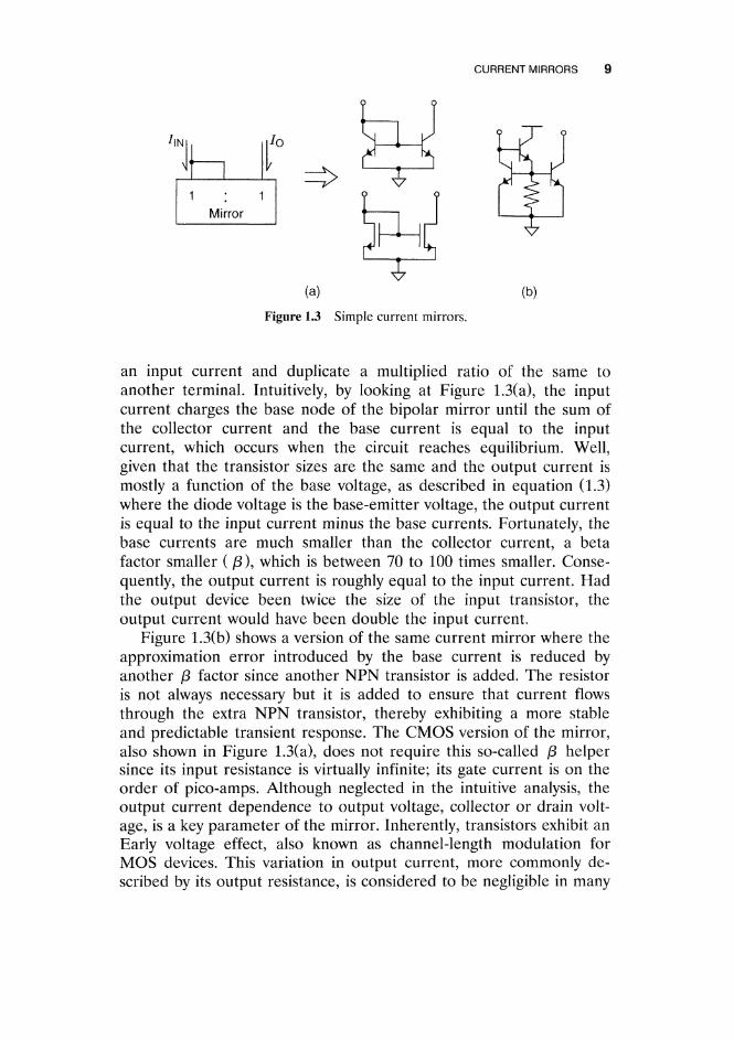
Current mirrors are widely used in basically all reference circuits.Consequently, a brief look at their operation and design considera-tions is justified. Figures 1.3 through 1.6 illustrate various bipolar andCMOS implementations of the current mirror, ranging from "simple"to regulated cascode mirrors. The basic function of a mirror is to take
\ Vgo - VBE(Tr) + (V - x)VTiT
Tr
'Vso + (v-x)VTi'VBE*
T Tr!
T-T+Tr\
CURRENT MIRRORS 9
Figure 1.3 Simple current mirrors.
an input current and duplicate a multiplied ratio of the same toanother terminal. Intuitively, by looking at Figure 1.3(a), the inputcurrent charges the base node of the bipolar mirror until the sum ofthe collector current and the base current is equal to the inputcurrent, which occurs when the circuit reaches equilibrium. Well,given that the transistor sizes are the same and the output current ismostly a function of the base voltage, as described in equation (1.3)where the diode voltage is the base-emitter voltage, the output currentis equal to the input current minus the base currents. Fortunately, thebase currents are much smaller than the collector current, a betafactor smaller (/3), which is between 70 to 100 times smaller. Conse-quently, the output current is roughly equal to the input current. Hadthe output device been twice the size of the input transistor, theoutput current would have been double the input current.
Figure 1.3(b) shows a version of the same current mirror where theapproximation error introduced by the base current is reduced byanother ft factor since another NPN transistor is added. The resistoris not always necessary but it is added to ensure that current flowsthrough the extra NPN transistor, thereby exhibiting a more stableand predictable transient response. The CMOS version of the mirror,also shown in Figure 1.3(a), does not require this so-called j3 helpersince its input resistance is virtually infinite; its gate current is on theorder of pico-amps. Although neglected in the intuitive analysis, theoutput current dependence to output voltage, collector or drain volt-age, is a key parameter of the mirror. Inherently, transistors exhibit anEarly voltage effect, also known as channel-length modulation forMOS devices. This variation in output current, more commonly de-scribed by its output resistance, is considered to be negligible in many
^INj /o
1 1Mirror
(a) (b)
10 THE BASICS
integrated circuits but not so in the design of references, where smallchanges in current can be significant. Cascode mirrors, consequently,are often used since they produce more accurate results.
1.2.1 The Simple Mirror
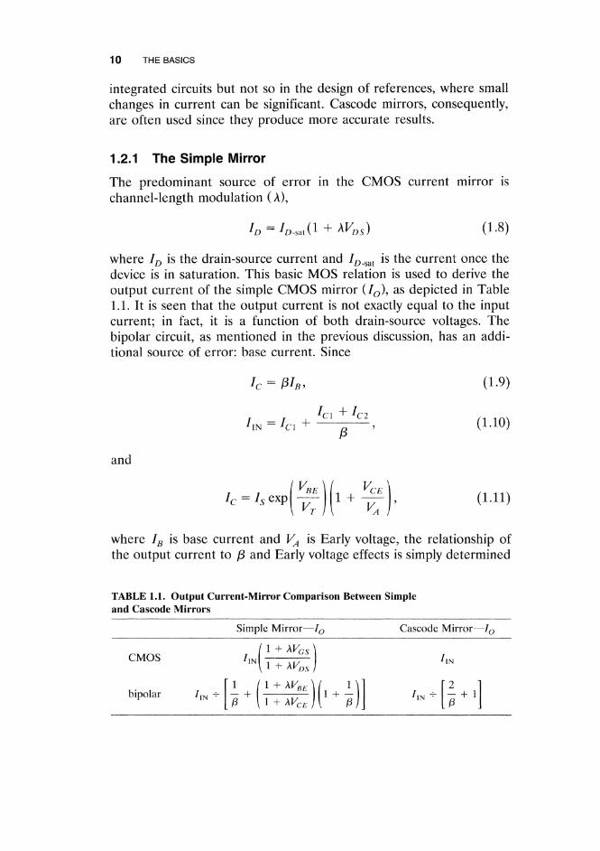
The predominant source of error in the CMOS current mirror ischannel-length modulation (A),
/ D - W 1 + AKD5) (1.8)
where ID is the drain-source current and JD_sat is the current once thedevice is in saturation. This basic MOS relation is used to derive theoutput current of the simple CMOS mirror (Io\ as depicted in Table1.1. It is seen that the output current is not exactly equal to the inputcurrent; in fact, it is a function of both drain-source voltages. Thebipolar circuit, as mentioned in the previous discussion, has an addi-tional source of error: base current. Since
lc = Ph>
MN ~ *C\
and
Ic = Is expK,
lex + hi
P
BE
V-r1 +
V,CE
VA
(1.9)
(1.10)
(1.11)
where IB is base current and VA is Early voltage, the relationship ofthe output current to /3 and Early voltage effects is simply determined
TABLE 1.1. Output Current-Mirror Comparison Between Simpleand Cascode Mirrors
Simple Mirror—Io Cascode Mirror—I,o
CMOS
bipolar
1 + XV,GS
AN :
1 + KVDS
1 + XVBE
1 + \VCE1 4- AN - I -
P
Icl + IC2
(1.11)
(1.10)
1 \]P}\
AN
1
2
./3Pr i
AN

CURRENT MIRRORS 11
by combining the above relations and collecting terms. The resultingequation is shown in Table 1.1. Connecting another NPN transistor, asshown in Figure 1.3(b), from the collector to the base of the inputtransistor minimizes the aforementioned fi error at the cost, ofcourse, of headroom limitations, two base-emitter voltages instead ofjust one. Overall, the output resistance of the simple mirror is compa-rable in both CMOS and bipolar technologies. The bandwidth isgreater, the noise is lower, and the matching capability is better forthe bipolar version, though. However, these benefits come at theexpense of more current error resulting from j8 effects.
1.2.2 Cascode Mirrors
The evolution from the simple mirror to the cascode counterpart isreadily apparent, shown in Figure 1.4. A couple of cascode devices areadded to ensure that the drain-source or collector-emitter voltages ofboth input and output transistors are the same, thereby practicallyeliminating channel-length modulation and Early voltage effects. Thevoltage at the base or gate of these devices is simply a low-precisionsteady-state bias voltage, which may be generated by running somecurrent through a resistor and/or diode-connected transistor. Theresulting output resistance is therefore increased. In particular, it isincreased by the product of the transconductance and the outputresistance of the cascading device for the CMOS case and by a /3factor for the bipolar circuit. Consequently, the much-improved input-to-output current relations shown in Table 1.1 result where the outputcurrent is essentially independent of drain-source and collector-emittervoltages.
Figure 1.4 Cascode current mirrors.
VBVB

12 THE BASICS
Figure 1.5 P-type cascode current-mirror example.
Design Example 1.1: Design a low-voltage, one-to-one, cascodecurrent mirror (input current equals 10 //A, DC) whose outputvoltage is greater than 0.6 V below the positive supply voltage. Theinput and the output currents flow away from the mirror. Assume thata biCMOS process, with a minimum channel length for MOS devicesof 1 ptm, is to be used.
Since MOS devices are available and accuracy is best achieved withthese transistors, p-type MOS transistors are chosen for the task.Figure 1.5 illustrates the circuit. Transistors mpl and mp2 constitutethe basic mirror while transistors mp3 and mp4 are the cascodingdevices. Resistor R is simply used to generate a bias voltage for thegates of mp3 and mp4. Since the output voltage can swing up to within0.6 V of positive supply VDEn the sum of the saturation voltages acrossmp2 and mp4 must be less than 0.6 V. Since the mirror ratio isone-to-one, mpl and mp2 must also be equal in size. For best results,mp3 and mp4 should also be the same size to ensure equal voltages atthe drains of mpl and mp2. The low overhead voltage of 0.6 V isarbitrarily chosen to be distributed equally between mp2 and mp4.Thus, choosing a saturation voltage (Ksat) of 0.25 V for all devicesyields
v ~ v = v = v =" sa t l Ksat2 y sat3 Ksat4
21 r
K'(W/L)
21 IN
K'{W/L)< 0.25 V,
mp4mp3
mpl
VDD.
+>CO
dA
mp2
R
IoI\H

CURRENT MIRRORS 13
where K' is assumed to be 15 /xA/V2. The aspect ratio of all fourdevices is therefore chosen to be 25 /xm//xm,
2/ IN 2(10/*)(W/L) > F<a5F) " (15,0(0.25') = 2 1 3 " m / " m -
Critical device mpl and device mp2 must match well for goodoverall performance of the mirror; hence, their channel length ischosen to be six times larger than the minimum allowed by the processto minimize channel-length modulation (i.e., 6/xm). The channel-length modulation effects of the cascoding devices on the outputcurrent are not as significant. As a result, their channel length ischosen to minimize area (i.e., 2 /xm). Consequently, the dimensions(W/L) chosen for mpl through mp4 are 150/6 /xm/^tm, 150/6/xm//xm, 50/2 /xm/^im, and 50/2 /xm/jLtm, respectively.
Finally, to ensure proper operation when the output voltage iswithin 0.6 V of the positive supply, the source-drain voltage of mpland mp2 is designed to be roughly 0.3 V, which would allow theoutput voltage to swing within 0.55 V of the positive supply (0.3V + Vmt). The following loop equation is consequently used to ascer-tain the value of the resistor:
VSGI + VR - VSG3 - VSDl = 0 = VSGl + VR- VSG3 - 0.3 V.
Since VSGl is equal to VSG, (same aspect ratio and equal currentdensities), they cancel and the voltage across the resistor is simplydesigned to be 0.3 V, which means R is 30 kO,
0.3 V 0.3 Vi ? = — - = ——== 30 k(l.
/IN 10/i,
1.2.3 Regulated Cascode Mirrors
A current mirror is actually a single-stage amplifier with negativefeedback. The input NPN transistor in Figure 1.3(a) is a common-emitter amplifier whose output, the collector terminal, is connected toits input, the base terminal, for negative feedback. The output currentis therefore regulated against the input current. Similarly, a cascodedevice uses a common-gate or common-base amplifier stage to in-crease the output resistance of the overall circuit. However, its regula-tion performance may be further increased if higher open-loop gain

14 THE BASICS
(b) (c)
Figure 1.6 Regulated cascode mirrors.
were to be introduced in the cascode gain stage. Regulated cascodemirrors do just that. The output resistance of the current mirror isconsequently boosted by a factor equal to that additional gain. Figure1.6 shows some CMOS as well as bipolar implementations of regu-lated cascode mirrors [5,6].
Figure 1.6(a), in particular, is a two-step evolution of the CMOS-regulated cascode circuit, from a high-voltage to a low-voltage circuit.In the final version, there is local feedback in addition to level shiftingto assure a low voltage across the drain-source voltage of mnl (VDSl).Low voltage is desired to extend the working range of the mirror (i.e.,the output voltage range for which the current is still regulated). Theadditional current source that is added to device mn2 (IB) is used tomatch the current flowing through mnl, which is IB + Jo , to avoidoutput current errors. Transistors mn3 and mn4 are designed to havea gate-source voltage difference equal to VDSl, which is designed to beclose to the saturation voltage of mnl to maximize output voltagerange.
JIN /o
IY Yp-A
(VY~VX)gmSVx
Io
RDSS
#DS1
qn2
& 1
I\M
IN qn5
(a)
l9 ZCJB ^ohl\n
IBhu mn5
mn3 mn4
mr»2 mnl
h IB2 mjB2
qn3 qn4
qn1
CURRENT MIRRORS 1 5
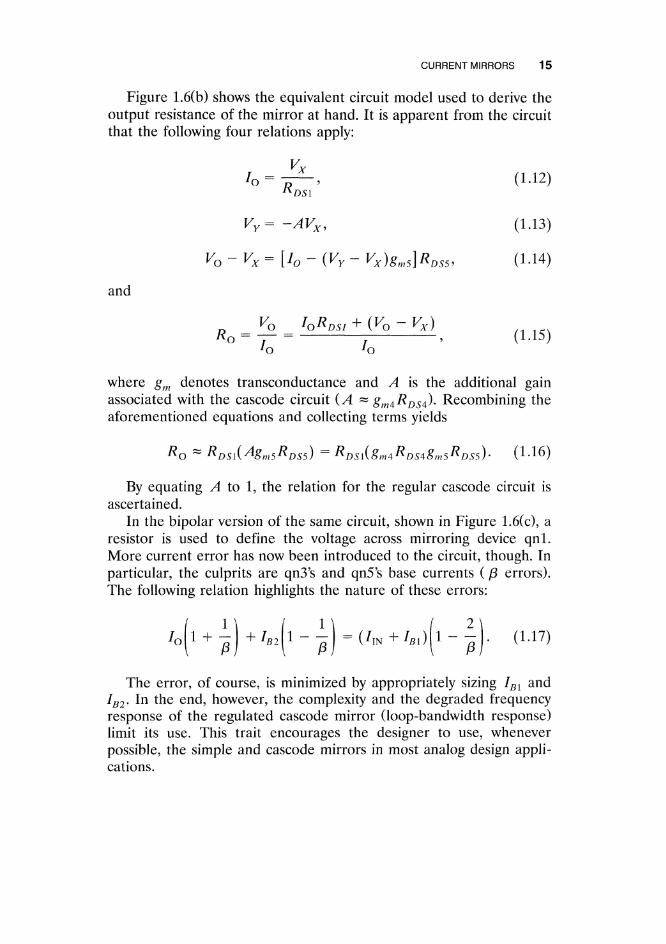
Figure 1.6(b) shows the equivalent circuit model used to derive theoutput resistance of the mirror at hand. It is apparent from the circuitthat the following four relations apply:
VxIo=-~-, (1.12)
KDSl
VY= -AVX9 (1.13)
Vo-Vx= [Io - (VY - Vx)gm5]RDS59 (1.14)
and
Vo IoRDSl + (Vo - Vx)Ro = — = — , (1.15)
i o i o
where gm denotes transconductance and A is the additional gainassociated with the cascode circuit (A ~ gm4RDS4^ Recombining theaforementioned equations and collecting terms yields
Ro « RDS\(Agm5RDS5) = RDSl(Sm4RDS4Sm5RDS5)' (1-16)
By equating A to 1, the relation for the regular cascode circuit isascertained.
In the bipolar version of the same circuit, shown in Figure 1.6(c), aresistor is used to define the voltage across mirroring device qnLMore current error has now been introduced to the circuit, though. Inparticular, the culprits are qn3's and qnS's base currents (f3 errors).The following relation highlights the nature of these errors:
' o | l + ^ ) + ^ - ^ ) = ( ' l N + / * l ) ( l - | (1.17)
The error, of course, is minimized by appropriately sizing IBl andIB2. In the end, however, the complexity and the degraded frequencyresponse of the regulated cascode mirror (loop-bandwidth response)limit its use. This trait encourages the designer to use, wheneverpossible, the simple and cascode mirrors in most analog design appli-cations.
KDSI
Vx(1.12)
(1.13)
(1.14)Vo-Vx^[l0-(VY-Vx)gm5]RDS5,
VY= -AVX,
Io
Io Io
Vo IoRDSl + (Vo ~ Vx)(1.15)* o =
p] BZ\ p) v " OI/\ p( A N +
1 \ / 1 \ / 2Io 1

16 THE BASICS
1.3 SUMMARY
Junction diodes are key elements in the design of references. They arenot necessarily a requirement but they are certainly useful whenseeking high performance at a reasonable cost. This trait arisesbecause the p-n junction voltage has a relatively high initial accuracy.Additionally, the electrical characteristics are repeatable, predictable,and well characterized over a wide range of currents and tempera-tures. Consequently, most current and voltage references ultimatelyuse these p-n junction diodes as the intrinsic building blocks in theirrespective designs.
Generally, references are an essential part of most, if not all,electrical systems. Although highly accurate precision references areusually desired, they are not always necessary. Rudimentary refer-ences are often sufficiently accurate to satisfy the demands of manyapplications. As a result, the complexity of the circuits varies from onedesign to the next. A simple reference may be a naturally existingvoltage that does not change significantly with operating conditions,like the p-n junction diode. Precision references, however, improveaccuracy by attempting to cancel the linear and nonlinear componentsof a given voltage. At this point, though, the basic tools with whichreferences are designed have been explored (i.e., diodes and currentmirrors). These are used in a variety of combinations to producetemperature-dependent currents and voltages, which eventually be-come key elements in the design of precision reference circuits. Thenext chapter deals with the generation of these temperature-depen-dent current references.
APPENDIX A.1 TEMPERATURE DEPENDENCEOF THE DIODE VOLTAGE
The collector current of a bipolar transistor exhibits an exponentialrelationship to the base-emitter voltage and is nominally expressed as
/ c = / ,exp ^ , (A.1.1)
where Ic is the collector current, Is is the saturation current in theforward-active region, VBE is the base-emitter (diode) voltage, and VT
is the thermal voltage. The effects of Early voltage are neglected for
VT .vBE\/ c = /5exp (A.l.n

APPENDIX A.1 TEMPERATURE DEPENDENCE OF THE DIODE VOLTAGE 17
this derivation. Consequently, VBE is derived to be
VBE = VT In Ic (A.1.2)
The saturation current Is is defined by the electron charge q (L6 X10 ~19 Coulomb), the intrinsic carrier concentration ni (approximately1.5 X 1010 cm"3 at 300 °K for silicon), the diffusion constant forelectrons DtV the emitter cross-sectional area Ae, the effective widthof the base WB, and the base-doping density NA (assumed to beconstant) [7],
qn]DnA qnJDlA,7^w- = iV^' (A-L3)
where QB is the number of doping atoms in the base per unit area ofemitter and TTn is the average effective value of the electron diffusionconstant in the base. The notation is consistent with NPN transistorsbut the theory also applies to PNP devices. The temperature depen-dence of the intrinsic carrier concentration and the average electrondiffusion constant can be described by [8]
n^=AT3txp^-^ (A.1.4)VT
and
rr=Kr^, (A.i.5)
where A is a temperature-independent constant, T is absolute tem-perature, Vgo is the extrapolated diode voltage at 0 °K, and fjun is theaverage mobility for minority carriers in the base,
K = BT-\ (A.1.6)
where B and n are temperature-independent constants. The relation-ship for the saturation current Is is more explicitly expressed by
, ^s i
*sqn]DnA
WBNA
qn]DltAe
QB(A.I.3)
A, = vTlLn, (A.1.5)
Hn = BT~\ (A.1.6)
-V

18 THE BASICS
substituting equations (A. 1.4) - (A. 1.6) in (A. 1.3), resulting in
<?
As ~
^4T3exp-Kgo
VT
\(VTBT-»)Ae
QB(A.1.7)
or
Is = CT(4-">exp -vn.VT
(A.I.8)
where C is a temperature-independent constant defined by all theconstants in equation (A.1.7), such as q, A, B, Ae, QB, and k/q fromthe thermal voltage term (VT = kT/q, where k is Boltzmann's con-stant: 8.62 X 10 ~5 eV/° K). Finally, the collector current can beassumed to have a temperature dependence whose behavior can bedescribed by
Ic = DTX, (A.I.9)
where D is a constant and x is an arbitrary number defined by thetemperature dependence of the current forced through the collector;i.e., x is 1 for a proportional-to-absolute temperature (PTAT) current(Ic a T1). Consequently, the temperature dependence of the base-emitter voltage can be reexpressed by substituting equations(A.1.8MA.1.9) in (A.1.2), resulting in
VBE = VT InD_T(*-(4-n))e x p
c VT
= Vgo + VT l n ( ^ ) - [(4 -n)- x]VT In T. (A.1.10)
However, a more appropriate form of the base-emitter relationship,for the purpose of design, is its temperature dependence as a functionof a reference temperature (Fr). This form can be derived by obtainingthe relation of the base-emitter voltage (VBE) at a reference tempera-ture (Tr), solving for a constant, and substituting it back in equation
C )
D
VTj
Ko

APPENDIX A.1 TEMPERATURE DEPENDENCE OF THE DIODE VOLTAGE 19
(A.I.10). The relation of VBE at Tr is
VBE(Tr) = Vgo + VTr I n ( ^ ) - [(4 - n) ~~ x]VTr lnT r, (A. l . l l )
where F r is the thermal voltage evaluated at the reference tempera-ture Tr. At this point, the constant is derived to be
ID\ _ VBE(Tr)-Vgo + [(A-n)~x]VTilnTrln|-j- - . (A.1.12)
Now, equation (A.1.12) is substituted back in (A. 1.10) to yield thewell-known temperature dependence relationship of the base-emittervoltage,
VBE = ygo - Y\VSO - VBE(Tr)} - [(4 - /i) -x]VT Inly
(A.1.13)
It is often useful to develop the Taylor series expansion of thelogarithmic term and substitute it back in equation (A.1.13). Thepurpose for the expansion is to more accurately design the cancella-tion of the linear as well as the curvature-correcting component of thebandgap reference. The process-dependent constant (4 - n) is some-times expressed as rj with an approximate value between 3.6 and 4 [4].The VBE relationship can be rewritten as
VBE=A+BT+Cf(T), (A.1.14)
where A, B, and C are constants and f(T) represents all the termswhose order is greater than 1 (i.e., C2T
2 + C3T3 + ••• +CnT
n. Nowthe Taylor series expansion of the logarithmic term about the refer-ence temperature Tr can be developed,
T I T-Oj-*)*7--ln -
(V-x)Vr
Tr«o + 1!
| a2(T~Tr)2 | | an(T-TrY
2! n\(A.1.15)
yTr
VBE(T,.) - Vgo + [(4 - n) - x]VTi In Tr(A.1.12)D\ \
Cin
Jr)
' T\• rj-<
T-iv-xW,
Cf(T),
ID
C
19
a^T-T,.)1
20 THE BASICS
w h e r e t he coefficients aO9al9...9an a r e descr ibed by
/ T
ah =*V*\T,
dkT T=T,.(A.I.16)
Equations (A.1.13), (A.1.15), and (A.1.16) are then used to derive thecoefficients of equation (A. 1.14) explicitly,
KBJ!.«BE v n -(V-x)Vr
go-(a0 -axTr)\
Ko-VBE(Tr) ai(r,-x)VTr
z.(V-x)Vr
+
T,- T i n
Z
Tr
-ao-ai(T-Tr)\) (A.1.17)
or
VBE=[Vgo + (71-x)VT]Vgo - VBE(Tr) + (r, - x)VTr
(r,-x)VTrTin — \-T+Tr (A.I.18)
which are variations of the relations offered by [8] and [9]. Givenequations (A.I.14) through (A.I.18), higher-order terms like T2, T3,etc. can also be derived. It is noteworthy to mention that thesehigher-order terms will affect the lower terms since the expansion isdone about temperature Tr, e.g., (T - Tr)
2 = (Tf2) - (2Tr)T + T2.
BIBLIOGRAPHY
[1] R. Kenyon, "A Quick Guide to Voltage References," EDN, no. 8, pp.161-167, April 13, 2000.
[2] AS. Sedra and K.C. Smith, Microelectronic Circuits. New York: Holt,Rinehart and Winston, 1987.
[3] A. Hastings, The Art of Analog Layout. New Jersey: Prentice-Hall, Inc.,2001.
T
Tr /
Tr
T\
Tr
T
Tr

BIBLIOGRAPHY 21
[4] M. Gunawan et. al., "A Curvature-Corrected Low-Voltage BandgapReference," IEEE Journal of Solid-State Circuits, vol. 28, no. 6, pp.667-670, June 1993.
[5] A.L. Coban and P.E. Allen, "A 1.75 V Rail-to-Rail CMOS Op Amp,"Proceedings IEEE International Symposium on Circuits and Systems, vol. 5,pp. 497-500, 1994.
[6] M. Helfenstein et. al., "90 dB, 90 MHz, 30 mW OTA with the Gain-Enhancement Implemented by One- and Two-Stage Amplifiers," Pro-ceedings IEEE International Symposium on Circuits and Systems, vol. 3,pp. 1732-1735, 1995.
[7] P.R. Gray and R.G. Meyer, Analysis and Design of Analog IntegratedCircuits. New York: Wiley, 1993.
[8] Y.P. Tsividis, "Accurate Analysis of Temperature Effects in Ic - Vbe
Characteristics with Application to Bandgap Reference Sources," IEEEJournal of Solid-State Circuits, vol. SC-15, no. 6, pp. 1076-1084, Decem-ber 1980.
[9] G.M. Meijer et. al., "A New Curvature-Corrected Bandgap Reference,"IEEE Journal of Solid-State Circuits, vol. SC-17, no. 6, pp. 1139-1143,December 1982.


![Active Subwoofer System SB-WA720PP - Philips d559 b0aack000004 diode [m] d560 b0aack000004 diode [m] d561 b0ba01200008 diode [m] d562 b0aack000004 diode [m] d563 b0ba01900005 diode](https://static.fdocuments.in/doc/165x107/5baed8c209d3f290738dc283/active-subwoofer-system-sb-wa720pp-philips-d559-b0aack000004-diode-m-d560-b0aack000004.jpg)
