The Agilent Device Modeling flow for Agilent DynaFET GaN ......Nonlinear Ids, Igs, Igd, Cgs, Cgd...
37
An overview of conventional and new modeling flows with emphasis on the new Agilent DynaFET GaN and GaAs FET model Amplifier Design Flow Seminar Basking Ridge, NJ, April 2 nd Authors: Roberto Tinti, Jianjun Xu, and David E. Root Presenter: Roberto Tinti The Agilent Device Modeling flow for nonlinear RF applications
Transcript of The Agilent Device Modeling flow for Agilent DynaFET GaN ......Nonlinear Ids, Igs, Igd, Cgs, Cgd...

An overview of conventional and new
modeling flows with emphasis on the new
Agilent DynaFET GaN and GaAs FET model
Amplifier Design Flow Seminar
Basking Ridge, NJ, April 2nd
Authors: Roberto Tinti, Jianjun Xu, and David E. Root
Presenter: Roberto Tinti
The Agilent Device
Modeling flow for
nonlinear RF
applications

Acknowledgement
Technical contributors Prof. I. Angelov
J. Xu
M. Iwamoto
J. Horn
T. Nielsen
M. Marcu
J. Verspecht
R. M. Biernacki
C. Gillease
F. Sischka
External collaborators: listed on specific slides
Others
R. Hoft
Agilent Management
Partner Company Management
4/2/2014
Amplifier Design Flow Seminar
3
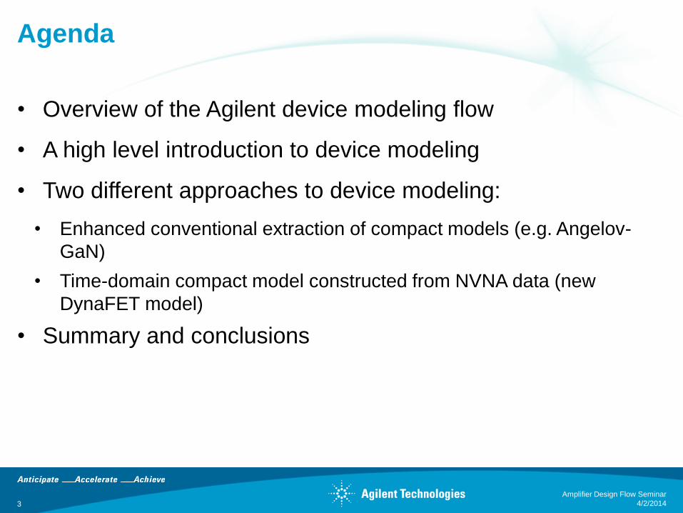
Agenda
• Overview of the Agilent device modeling flow
• A high level introduction to device modeling
• Two different approaches to device modeling:
• Enhanced conventional extraction of compact models (e.g. Angelov-
GaN)
• Time-domain compact model constructed from NVNA data (new
DynaFET model)
• Summary and conclusions
4/2/2014
Amplifier Design Flow Seminar
4
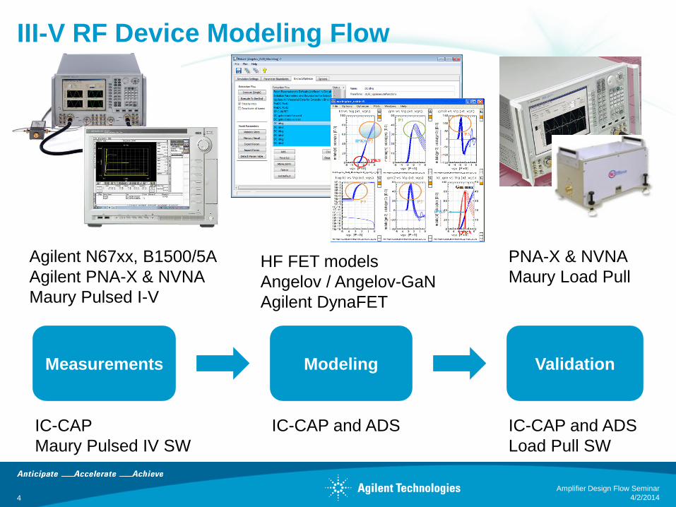
III-V RF Device Modeling Flow
Measurements Modeling Validation
Agilent N67xx, B1500/5A
Agilent PNA-X & NVNA
Maury Pulsed I-V
IC-CAP
Maury Pulsed IV SW
HF FET models
Angelov / Angelov-GaN
Agilent DynaFET
IC-CAP and ADS IC-CAP and ADS
Load Pull SW
PNA-X & NVNA
Maury Load Pull
4/2/2014
Amplifier Design Flow Seminar
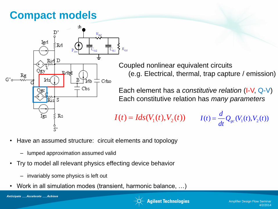
Compact models
• Have an assumed structure: circuit elements and topology
– lumped approximation assumed valid
• Try to model all relevant physics effecting device behavior
– invariably some physics is left out
• Work in all simulation modes (transient, harmonic balance, …)
Coupled nonlinear equivalent circuits
(e.g. Electrical, thermal, trap capture / emission)
Each element has a constitutive relation (I-V, Q-V)
Each constitutive relation has many parameters
1 2( ) ( ( ), ( ))I t Ids V t V t1 2( ) ( ( ), ( ))gc
dI t Q V t V t
dt
4/2/2014
Amplifier Design Flow Seminar
6
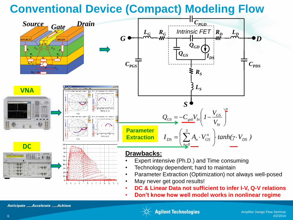
Conventional Device (Compact) Modeling Flow
bi
GSbigs0GS
V
V1VCQ
QGS IDS
QGD
CPGS CPDS
CPGD
LG RD LD
RS
LS
RG
G D
S
Intrinsic FET
)Vtanh(γVAI DS
3
0n
n
GSnDS
VNA
DC
Parameter
Extraction
Gate Drain Source
Drawbacks: • Expert intensive (Ph.D.) and Time consuming
• Technology dependent; hard to maintain
• Parameter Extraction (Optimization) not always well-posed
• May never get good results!
• DC & Linear Data not sufficient to infer I-V, Q-V relations
• Don’t know how well model works in nonlinear regime
4/2/2014
Amplifier Design Flow Seminar

7
The Angelov-GaN model Non linear device model for GaAs and GaN developed at Chalmers by Prof. I. Angelov
• Empirical equivalent circuit model
• Well defined extraction procedure
• Available in all major simulator via Verilog-A implementation
• Include models for all key effects, including dispersion & breakdown
Nonlinear Ids, Igs, Igd, Cgs, Cgd
Idss
Igs
Igd
Ids
4/2/2014
Amplifier Design Flow Seminar
How does Angelov compares to EEHEMT
2014/4/10
Agilent Restricted
EEHEMT Angelov / Angelov-GaN
Model Equation Type
Piecewise
Continuous
Extension for GaN Devices
Asymmetric Capacitance
Modeling
Drain-Voltage Dependent
Capacitance Modeling
Self Heating Effect
(PEFF, MU)
(RTH, CTH)
Frequency Dispersion of
Conductance
Series RC branch
+ Dispersion current
(Separate parameters for DC/AC)
Series RC branch
+ Nonlinear R
Temperature Dependency
Modeling
Convergence in LS
Simulation
Geometry Scaling
Noise Modeling
1. Provide good
performance
when modeling
high-order
derivatives of
Drain current (and
harmonics)
2. Can be
implemented by
applying external
scaling equations
to model
parameters
3. Uses standard
noise model for
MESFET/HEMT
devices (+ 1/f
noise model)
Good modeled
Partially modeled
Not modeled
[1]
[2]
[3]
8
9
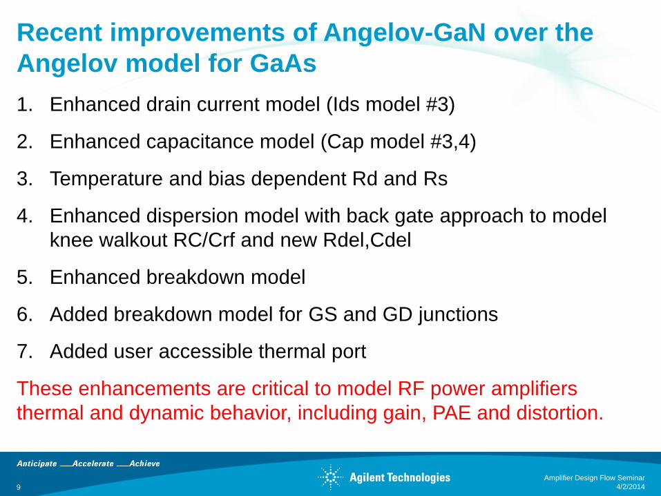
Recent improvements of Angelov-GaN over the
Angelov model for GaAs
1. Enhanced drain current model (Ids model #3)
2. Enhanced capacitance model (Cap model #3,4)
3. Temperature and bias dependent Rd and Rs
4. Enhanced dispersion model with back gate approach to model
knee walkout RC/Crf and new Rdel,Cdel
5. Enhanced breakdown model
6. Added breakdown model for GS and GD junctions
7. Added user accessible thermal port
These enhancements are critical to model RF power amplifiers
thermal and dynamic behavior, including gain, PAE and distortion.
4/2/2014
Amplifier Design Flow Seminar

10
Examples of Angelov-GaN improvements: over GaAs Angelov
PO
A
Y
X
Plot Angelov_GaN_Modeling/ac/spar_vg_vd/Cgs_vs_Vg
Cgs_vs_Vg (spar_vg_vd)
vgx [E+0]
sdata
(Cgs)
[E
-12]
-10 -8 -6 -4 -2 0 22
4
6
8
10
12
Angelov-GaN
(Capmod=3,4)
with Peaking Cap.
PO
A
Y
X
Plot Angelov_GaN_Modeling/ac/spar_vg_vd/Cgs_vs_Vg
Cgs_vs_Vg (spar_vg_vd)
vgx [E+0]
sdata
(Cgs)
[E
-12]
-10 -8 -6 -4 -2 0 22
4
6
8
10
12
14
Angelov
(or Capmod=0,1,2)
No Peaking Cap.
Cgs_vg Cgs_vg
Better fitting for
peaking Cgs
Gate Breakdown
Ids accuracy
is improved
- Measured
- Angelov-GaN Sim
- Angelov Sim
Enhanced capacitance and gate breakdown models
4/2/2014
Amplifier Design Flow Seminar
11
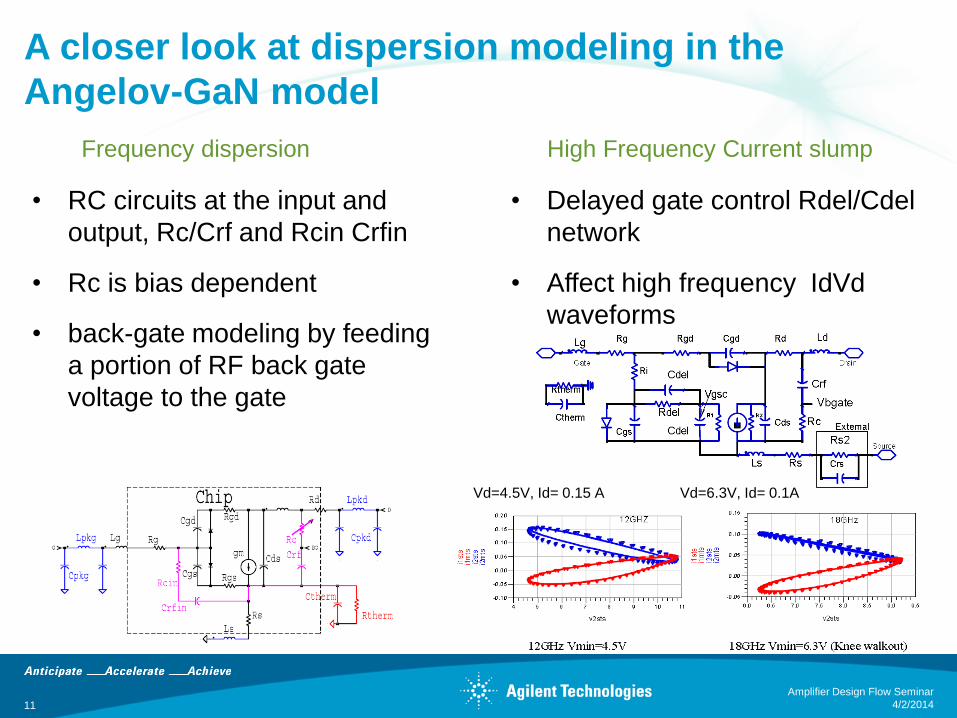
A closer look at dispersion modeling in the
Angelov-GaN model
• RC circuits at the input and
output, Rc/Crf and Rcin Crfin
• Rc is bias dependent
• back-gate modeling by feeding
a portion of RF back gate
voltage to the gate
Frequency dispersion
• Delayed gate control Rdel/Cdel
network
• Affect high frequency IdVd
waveforms
High Frequency Current slump
Vd=4.5V, Id= 0.15 A Vd=6.3V, Id= 0.1A
4/2/2014
Amplifier Design Flow Seminar

12
Angelov-GaN typical extraction flow
• DC measurements at
various temperatures
• Pulsed IV measurements
• S-parameters
measurements
• Large signal (Load pull or
NVNA or both)
• Parasitic extraction
• DC & Thermal
• AC
• Final optimization by using
DC, small signal and large
signal data
• Independent Large signal
validation (LP or NVNA)
Measurements Modeling
4/2/2014
Amplifier Design Flow Seminar

Extraction Flow with IC-CAP
Update Measured Data
(inc. de-embedding)
Extract System Series
Resistance
Repeat until getting
medium level fit
Extract CV
parameters
Repeat until getting
medium level fit
LS Verification
4/2/2014
Amplifier Design Flow Seminar
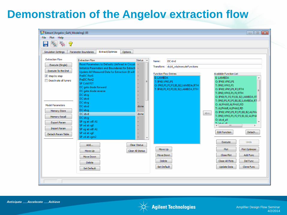
Demonstration of the Angelov extraction flow
4/2/2014
Amplifier Design Flow Seminar
15
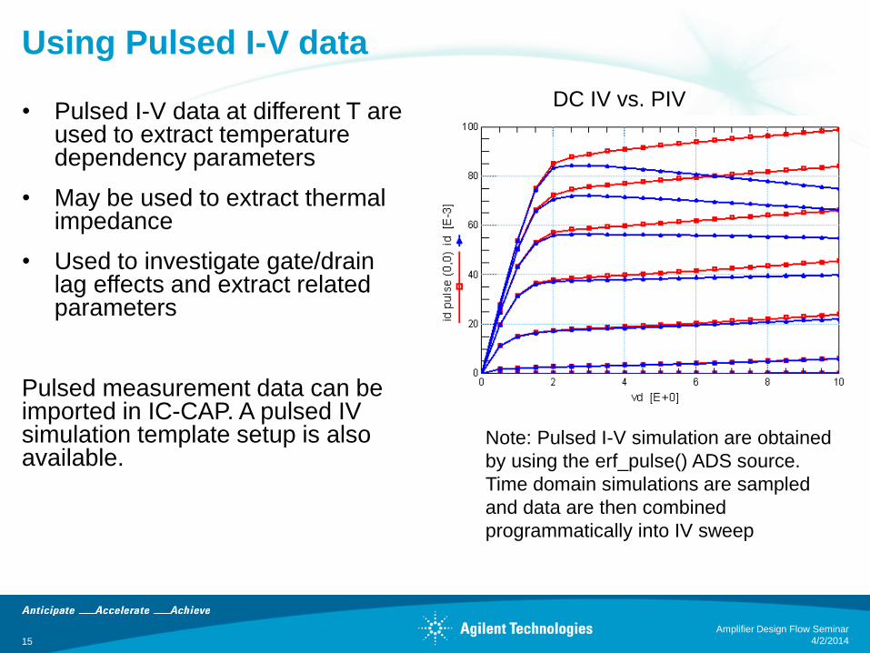
Using Pulsed I-V data
• Pulsed I-V data at different T are used to extract temperature dependency parameters
• May be used to extract thermal impedance
• Used to investigate gate/drain lag effects and extract related parameters
Pulsed measurement data can be imported in IC-CAP. A pulsed IV simulation template setup is also available.
Note: Pulsed I-V simulation are obtained
by using the erf_pulse() ADS source.
Time domain simulations are sampled
and data are then combined
programmatically into IV sweep
DC IV vs. PIV
4/2/2014
Amplifier Design Flow Seminar
16
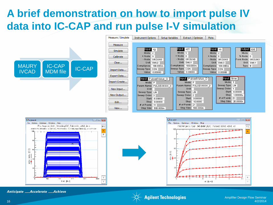
A brief demonstration on how to import pulse IV
data into IC-CAP and run pulse I-V simulation
MAURY IVCAD
IC-CAP MDM file
IC-CAP
4/2/2014
Amplifier Design Flow Seminar
17
Benefits of using large signal data in the
conventional extraction
• Get best set of parameter values for given model
• Trade-off fits at large-signal and small-signal – Tune parameters for specific applications
• Better extraction of parameters (such as breakdown and kirk
effect) that are based on behavior in limiting regions of
operation
• Explore limitations of the model
4/2/2014
Amplifier Design Flow Seminar

Measurements
Model
MOSFET
BSIM3.2 model
Using parameter values
extracted from DC + CV
Using parameter values
extracted from NVNA data
Measurements
Model
Vg
Ig
Vg
Ig
a11
b
a11
b
Measurements
Model
Measurements
Model
Conventional parameter extraction using large signal data
[10] E. Vandamme et al, “Large-signal network analyzer measurements and their use in device modeling,” MIXDES 2002, Wroclaw, Poland
• Get optimal parameter
set for given model
• trade-off DC, SP, for
nonlinear performance
• App-dependent tuning
• Explore model limits
4/2/2014
Amplifier Design Flow Seminar
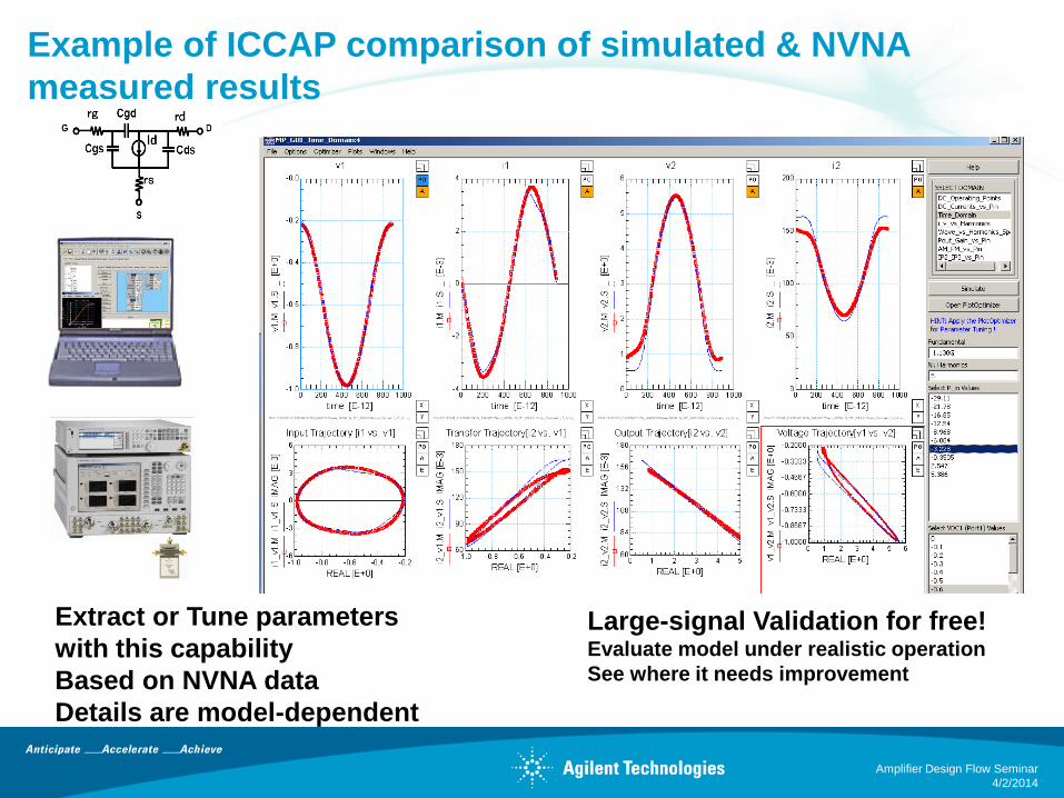
Example of ICCAP comparison of simulated & NVNA
measured results
Extract or Tune parameters
with this capability
Based on NVNA data
Details are model-dependent
Large-signal Validation for free! Evaluate model under realistic operation
See where it needs improvement
4/2/2014
Amplifier Design Flow Seminar

20
Conclusion about Angelov-GaN model
• Most popular GaN model, widely adopted in the industry,
available in ADS.
• Dynamic thermal and trapping effects are modeled via RC
networks.
• Basic extraction can be done using DC, pulsed IV and S-
parameter data
• Best results are obtained when parameters are tuned to large
signal data (LP or NWNA)
4/2/2014
Amplifier Design Flow Seminar
21
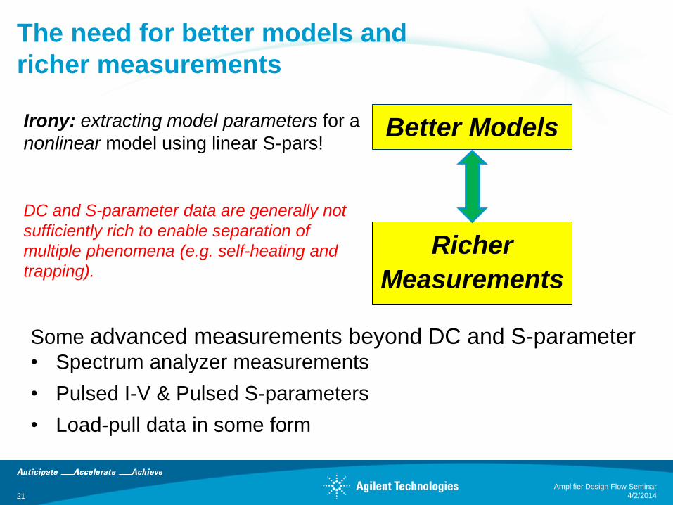
The need for better models and
richer measurements
Richer
Measurements
Better Models
Some advanced measurements beyond DC and S-parameter • Spectrum analyzer measurements
• Pulsed I-V & Pulsed S-parameters
• Load-pull data in some form
DC and S-parameter data are generally not
sufficiently rich to enable separation of
multiple phenomena (e.g. self-heating and
trapping).
Irony: extracting model parameters for a
nonlinear model using linear S-pars!
4/2/2014
Amplifier Design Flow Seminar

NVNA-based device
characterization
NVNA
Introducing the Agilent DynaFET, a complete
NVNA-based device modeling flow
ADS
IC design
Advanced compact model
constructed from NVNA data
[4] J. Xu, M. Iwamoto, J. Horn, D. E. Root, IEEE MTT-S International Microwave Symposium Digest, May, 2010.
4/2/2014
Amplifier Design Flow Seminar
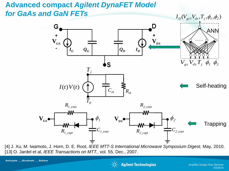
2_emitC
2
2_emitR
2_captR1_emitC
GSV 1
1_emitR
1_captR
)()( tV tIthC
thR
jT
0T
IG QG ID QD
DSV
GSV
DSV
Self-heating
Trapping
Advanced compact Agilent DynaFET Model
for GaAs and GaN FETs
dsgs V V 21j T
, ,T ,V ,VI 21jdsgsD )(
ANN
[4] J. Xu, M. Iwamoto, J. Horn, D. E. Root, IEEE MTT-S International Microwave Symposium Digest, May, 2010.
[13] O. Jardel et al, IEEE Transactions on MTT., vol. 55, Dec., 2007.
4/2/2014
Amplifier Design Flow Seminar
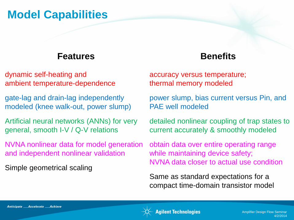
Model Capabilities
Features
dynamic self-heating and
ambient temperature-dependence
gate-lag and drain-lag independently
modeled (knee walk-out, power slump)
Artificial neural networks (ANNs) for very
general, smooth I-V / Q-V relations
NVNA nonlinear data for model generation
and independent nonlinear validation
Simple geometrical scaling
Benefits
accuracy versus temperature;
thermal memory modeled
power slump, bias current versus Pin, and
PAE well modeled
detailed nonlinear coupling of trap states to
current accurately & smoothly modeled
obtain data over entire operating range
while maintaining device safety;
NVNA data closer to actual use condition
Same as standard expectations for a
compact time-domain transistor model
4/2/2014
Amplifier Design Flow Seminar
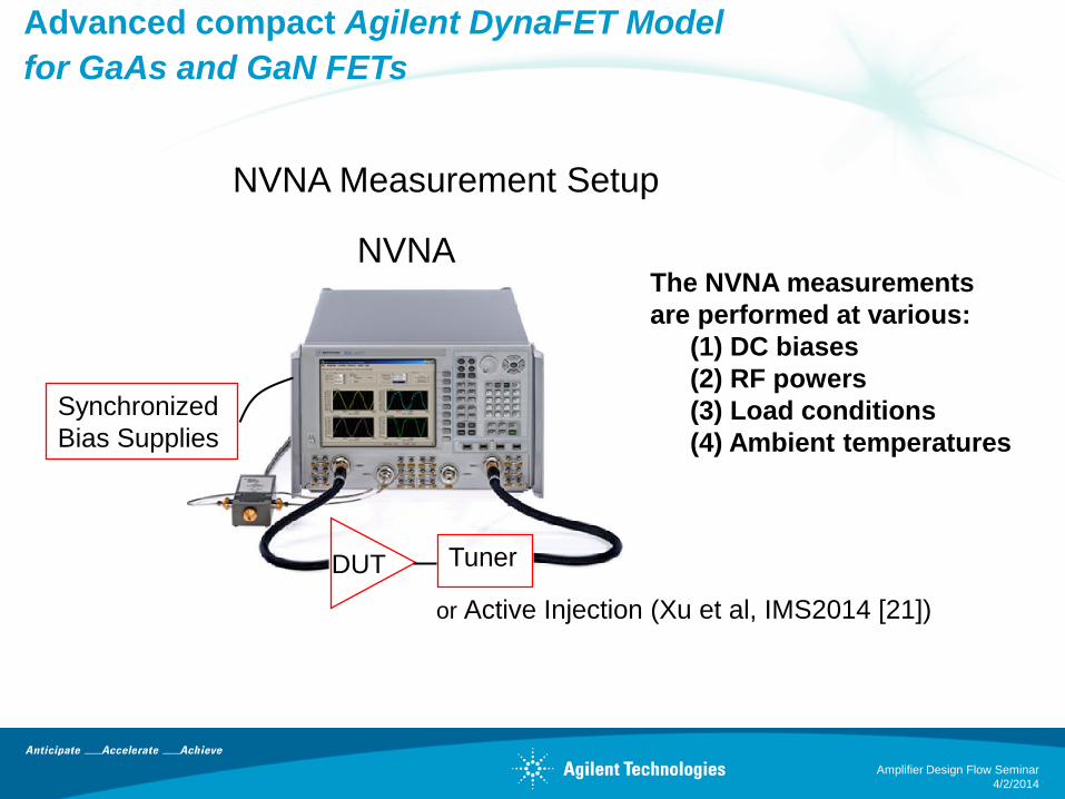
NVNA Measurement Setup
The NVNA measurements
are performed at various:
(1) DC biases
(2) RF powers
(3) Load conditions
(4) Ambient temperatures
DUT Tuner
NVNA
Synchronized
Bias Supplies
or Active Injection (Xu et al, IMS2014 [21])
Advanced compact Agilent DynaFET Model
for GaAs and GaN FETs
4/2/2014
Amplifier Design Flow Seminar
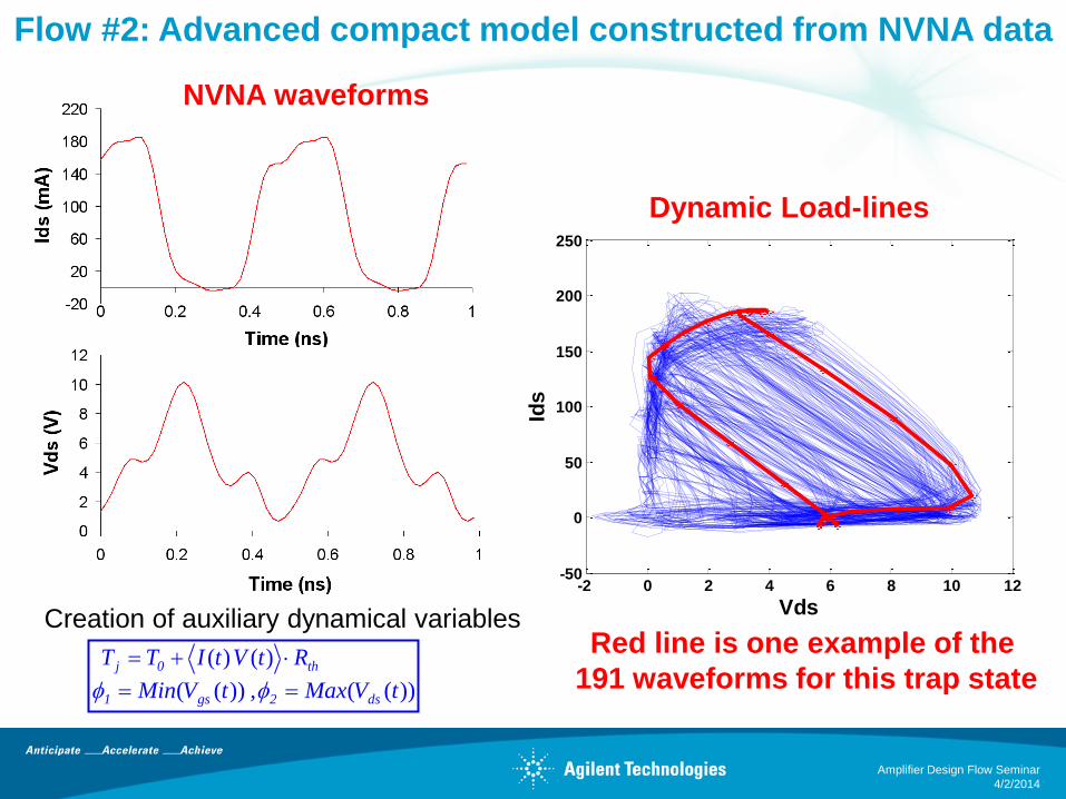
Flow #2: Advanced compact model constructed from NVNA data
Dynamic Load-lines
-2 0 2 4 6 8 10 12-50
0
50
100
150
200
250
Vds
Ids
Red line is one example of the
191 waveforms for this trap state th0j RtV tITT )()(
))(())(( tVMax ,tVMin ds2gs1
Creation of auxiliary dynamical variables
NVNA waveforms
4/2/2014
Amplifier Design Flow Seminar
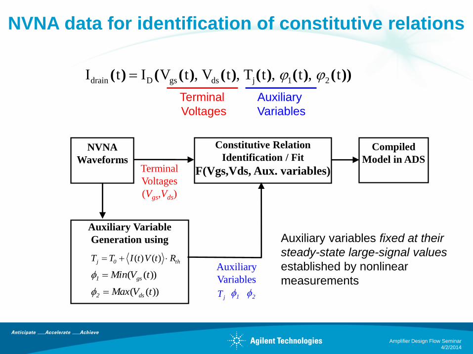
NVNA data for identification of constitutive relations
drain D gs ds j 1 2I t I V t , V t , T t , t , t ( ) ( ( ) ( ) ( ) ( ) ( ))
Auxiliary
Variables
Terminal
Voltages
NVNA
Waveforms
Auxiliary Variable
Generation using
Constitutive Relation
Identification / Fit
F(Vgs,Vds, Aux. variables) Terminal
Voltages
(Vgs,Vds)
Compiled
Model in ADS
th0j RtV tITT )()(
))(( tVMin gs1
))(( tVMax ds2
Auxiliary
Variables
jT 1 2
Auxiliary variables fixed at their
steady-state large-signal values
established by nonlinear
measurements
4/2/2014
Amplifier Design Flow Seminar
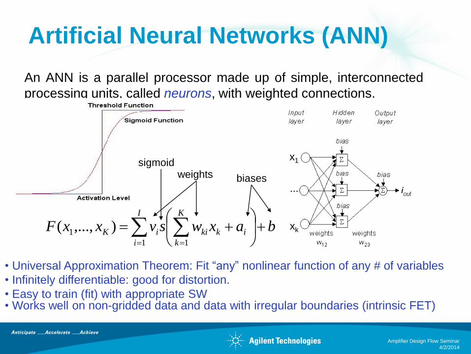
Artificial Neural Networks (ANN)
• Universal Approximation Theorem: Fit “any” nonlinear function of any # of variables
• Infinitely differentiable: good for distortion.
• Easy to train (fit) with appropriate SW • Works well on non-gridded data and data with irregular boundaries (intrinsic FET)
An ANN is a parallel processor made up of simple, interconnected
processing units, called neurons, with weighted connections.
baxwsvxxFI
i
K
k
ikkiiK
1 1
1 ),...,(
sigmoid weights biases
x1
...
xk
4/2/2014
Amplifier Design Flow Seminar
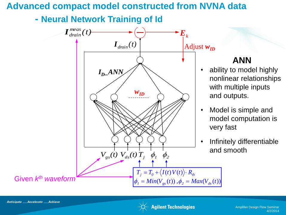
kE
Adjust wID
Given kth waveform
(t)meas
drainI
(t)V (t)V dsgs
th0j RtV tITT )()(
))(())(( tVMax ,tVMin ds2gs1
21j T
(t)drainI
ID_ANN
wID
ANN • ability to model highly
nonlinear relationships
with multiple inputs
and outputs.
• Model is simple and
model computation is
very fast
• Infinitely differentiable
and smooth
Advanced compact model constructed from NVNA data
- Neural Network Training of Id
4/2/2014
Amplifier Design Flow Seminar
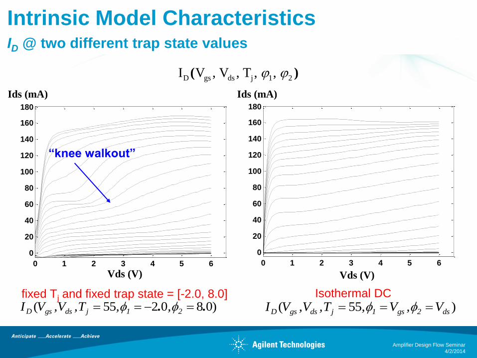
Intrinsic Model Characteristics ID @ two different trap state values
0 1 2 3 4 5 6
0
20
40
60
80
100
120
140
160
180
0 1 2 3 4 5 6
0
20
40
60
80
100
120
140
160
180
Vds (V)
Ids (mA) Ids (mA)
Vds (V)
fixed Tj and fixed trap state = [-2.0, 8.0] Isothermal DC )080255( .. 21jdsgsD , ,T ,V ,VI )55( ds2gs1jdsgsD V ,V ,T ,V ,VI
D gs ds j 1 2I V , V , T , , ( )
“knee walkout”
4/2/2014
Amplifier Design Flow Seminar
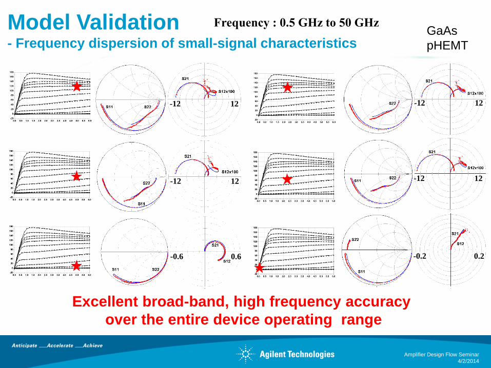
Model Validation - Frequency dispersion of small-signal characteristics
Excellent broad-band, high frequency accuracy
over the entire device operating range
-12 12
-12 12
-0.6 0.6
-12 12
-12 12
-0.2 0.2
Frequency : 0.5 GHz to 50 GHz GaAs
pHEMT
4/2/2014
Amplifier Design Flow Seminar

Simulated (___ )
Measured data (symbols)
Advanced compact model constructed from NVNA data
- Model validation: Harmonic distortion, gain, bias current vs. power
GaAs
pHEMT
4/2/2014
Amplifier Design Flow Seminar

0 2 4 6 8 10 12-20
0
20
40
60
80
100
120
140
160
180
200
Vds (V)
Id (mA) (.): DC
(o): Measured
Line: Simulated
Load
This Load was not used
in the model extraction
Demonstrates model can go far beyond the range over which
conventional DC and linear S-parameters can be taken
Advanced compact model constructed from NVNA data
- Model validation: Dynamic loadline
GaAs
pHEMT
4/2/2014
Amplifier Design Flow Seminar

DynaFET modeling flow: components & use model
ADS environment
External party environment Customer responsibility
PNA-X - NVNA DynaFET Characterization module
DynaFET meas. control SW
GUI
Active Source Injection control
DUT
info
input
Measurements
File transfer
Raw Data
Nonlinear
*for model generation
*for validation
DynaFET
natively
compiled model
tuners, DC supplies
external RF source,
bias tees, amps,
prober & probes
thermal chuck
model-file (ANN weights)
Encrypted
Agile
nt
pro
du
ct p
art
s
Custo
me
r
Resp
on
sib
ility
customer circuit
PNA-X NVNA environment
ICCAP environment
DynaFET Package
Characterization
DC I-V
SP
Parasitics Extraction
Extraction/de-embedding
DynaFET Core GUI
Extraction/Training
Validation
DC, SP
1-, 2-tone Pout/Pin
Raw Data DC I-V
SP
DynaFET Three-legged platform
0 1 2 3 4 5 6
0
20
40
60
80
100
120
140
160
180
“knee
walkout”
4/2/2014
Amplifier Design Flow Seminar
Summary
Conventional compact models have fundamental limitations, the
recent commercial availability of NVNA instruments provides new
alternatives:
• NVNA data for compact model parameter extraction/validation Tune parameters, optimal parameter set, validate model, explore limits
• NVNA data & ANN-based construction of advanced compact
Agilent DynaFET Model Very accurate and general model, with self-heating and trapping effects.
These are trends that are becoming useful now and are likely to
become increasingly important in the future.
“Every nonlinear modeling station should use an
NVNA instead of a conventional linear VNA.” - Dr. D. E. Root, Agilent Technologies
4/2/2014
Amplifier Design Flow Seminar
36
References [1] http://www.agilent.com/find/nvna
[2] Chiu et al “Characterization of annular-structure RF LDMOS transistors using Polyharmonic Distortion Model,” IEEE MTT-S International Microwave Symposium Digest, June, 2009, pp 977-980
[3] D. Gunyan et al, “Nonlinear validation of arbitrary load X-parameter and measurement-based device models,” IEEE MTT-S ARFTG Conference, Boston, MA, June 2009
[4] J. Xu, M. M. Iwamoto, J. Horn, D. E. Root, “Large-signal FET model with multiple time scale dynamics from nonlinear vector network analyzer data,” IEEE MTT-S International Microwave Symposium Digest, May, 2010.
[5] J. Horn, “Harmonic load-tuning predictions from X-parameters,” IEEE PA Symposium, San Diego, Sept. 2009
[6] G. Simpson et al, “Load-pull + NVNA = Enhanced X-parameters for PA designs with high mismatch and technology-independent large-signal device models,” IEEE ARFTG Conference, Portland, OR December 2008.
[7] J. Verspecht and D. E. Root, “Poly-Harmonic Distortion modeling,” in IEEE Microwave Theory and Techniques Microwave Magazine, June, 2006
[8] D. E. Root et al “X-parameters: The new paradigm for measurement, modeling, and design of nonlinear RF and microwave components,” Microwave Engineering Europe, Dec. 2008 pp 16-21.
[9] Agilent Advanced Design System documentation: Nonlinear Devices
[10] E. Vandamme et al, “Large-signal network analyzer measurements and their use in device modeling,” MIXDES 2002, Wroclaw, Poland.
[11] http://www.cree.com/products/pdf/CGH40010.pdf
[12] J. Horn, G. Simpson, and D. E. Root “GaN Device Modeling with X-Parameters,” IEEE MTT-S CSIC Symposium , Monterey, CA 2010.
[13] O. Jardel et al, “An electrothermal model for AlGaN/GaN power HEMTs including trapping effects to improve large-signal simulation results on high VSWR,” IEEE Transactions on MTT., vol. 55, Dec., 2007.
[14] J Verspecht, "Black box modelling of power transistors in the frequency domain," INMMiC'96 Conference Record, Duisburg, 1996
[15] J. Verspecht et al, “Extension of X-parameters to include long-term dynamic memory effects,” IEEE MTT-S International Microwave Symposium Digest, 2009. pp 741-744, June, 2009.
4/2/2014
Amplifier Design Flow Seminar
37
References (2)
[16] D. E. Root, “Future Device Modeling Trends,” IEEE Microwave Magazine, Nov./Dec. 2012, pp 45-59
[17] T. S. Nielsen, M. Dieudonne, C. Gillease, D. E. Root, “Doherty Power Amplifier Design in Gallium Nitride Technology Using a Nonlinear Vector Network Analyzer and X-Parameters,” IEEE Compound Semiconductor Integrated Circuit Symposium (CSICS), October, 2012.
[18] D. E. Root, J. Xu, F. Sischka, M. Marcu, J. Horn, R.M. Biernacki, M. Iwamoto, “Compact and Behavioral Modeling of Transistors from NVNA Measurements: New Flows and Future Trends,” IEEE Custom Integrated Circuits Conference Digest San Jose, Sept. 2012
[19] Roblin, P.; Root, D.E.; Verspecht, J.; Ko, Y.; Teyssier, J.P. , “New Trends for the Nonlinear Measurement and Modeling of High-Power RF Transistors and Amplifiers With Memory Effects,” IEEE Transactions Microwave Theory and Techniques, Volume: 60 , Issue: 6 , part 2: pp. 1964 – 1978, 2012
[20] Root, D. E.; Marcu, M.; Horn, J.; Xu, J.; Biernacki, R. M.; Iwamoto, M., “Scaling of X-parameters for device modeling,” IEEE MTT-S International Microwave Symposium Digest (MTT), June, 2012
[21] J. Xu, R. Jones, S. A. Harris, T. Nielsen, and D. E. Root, “Dynamic FET Model – DynaFET - for GaN Transistors from NVNA Active Source Injection Measurements,” To be presented at 2014 IMS, Tampa, June.
[22] J. Xu, S. Halder, F. Kharabi, J. McMacken, J. Gering, and D. E. Root, Submitted for publication.
[23] D. E. Root, J. Verspecht, J. Horn, and M. Marcu, X-Parameters, Cambridge University Press, 2013
[24] T. S. Nielsen, M. Dieudonne, C. Gillease, and D. E. Root, “Doherty power amplifier design in gallium nitride technology using a nonlinear vector network analyzer and X-parameters,” in IEEE CSICS Dig. , La Jolla, CA, Oct 2012.
4/2/2014
Amplifier Design Flow Seminar