The access point to develop
64
Transcript of The access point to develop

© im
ec
The access point to develop electronic components and systems

Dear customers, colleagues and friends,
What a year it has been! Who could have imagined that a worldwide pandemic would fall upon us in 2020. We sincerely hope that you have all managed to stay safe during this turbulent period. Even though it has been an unusual and difficult time, EUROPRACTICE has uninterruptedly continued to support its customers with access to microsystem technologies. The achievements obtained in 2020 are summarized in the new EUROPRACTICE Activity Report 2020-2021, which is in your hands now. We hope you will enjoy reading it and looking forward together with us to the new year where we can slowly return to normality.
Even though the majority of 2020 was affected by a global pandemic and related restrictions, it has been a very busy year. We realized a total of 896 design submissions in a wide range of technologies with 80% of the designs submitted by European universities, research institutes and companies. EUROPRACTICE offers a good technology mix for its customers. Advanced technologies, older technology nodes and More-than-Moore technologies are all used in significant volume by our customers. Notably, the total number of design submissions is slightly higher than for the previous year, which is remarkable for such an unusually difficult year as 2020. It demonstrates that research and innovation could continue at the same pace, and EUROPRACTICE together with its foundry partners have continued to support its customers despite the COVID-19 restrictions.
In 2020, the outreach activities from EUROPRACTICE were severely impacted by the global pandemic. Except for MEMS2020 and ISSCC2020, which were organized in January and February, all other conferences and exhibitions had to turn to a virtual format. Such online conferences and fairs have proven to be not as effective as their physical counterparts. EUROPRACTICE anticipated this by increasing its digital presence. For instance, regular news and updates were posted on our EUROPRACTICE LinkedIn account focusing on enlarging and strengthening our user community. Next to that, different webinar series were organized to create awareness in emerging fields such as Silicon Photonics, Microfluidics and Advanced Packaging. The majority of those webinars are uploaded to our YouTube channel, where anyone interested in those topics can watch them at their convenience. When it became clear that COVID-19 restrictions would remain for some considerable time, existing physical training courses were reconfigured and adapted so they could be presented online as live instructor-led training including (where appropriate) hands-on practical sessions using remotely accessible design tool environments.
In 2021, EUROPRACTICE will continue to deliver a high-quality service to customers. Thanks to the results of the customer survey, which has been conducted at the end of last year, we know even better how we can improve and enhance our services for the entire user community. Customers can access new technologies which were recently added to our portfolio, such as the Si-Photonics processes from LioniX International and CORNERSTONE. New virtual training courses and webinars will be developed and presented to a broad range of users, including traditional electronic sectors and non-traditional sectors (such as MedTech). Moreover, in 2021 the enhanced service offering towards smart system integration will be put more in the spotlight. Ultimately, EUROPRACTICE will act as a true one-stop shop for technologies enabling fully integrated systems and providing direct routes for industrial up-scaling of those systems. Consequently, it will contribute to creating and sustaining new jobs in Europe, especially in the areas of design and fabrication of microelectronic components and systems.
We thank the European Commission (DG Connect) for their support. In 2021, we will work towards an extension of our program within Horizon Europe. The EC funding ensures that we hold our commitment to continue the EUROPRACTICE service and to offer the European academic institutions and SMEs easy and affordable access to state-of-the-art design tools and IC technologies.
Finally, we thank all of you – our academic and industrial customers, our technology and design tool suppliers – for supporting our services, and we wish you all a more ‘normal’ 2021.
Looking forward to supporting your innovative projects and creating more success stories together.
Romano Hoofman (EUROPRACTICE General Manager)On behalf of the entire EUROPRACTICE team at imec, UKRI-STFC, FhG-IIS, CMP and Tyndall
FOREWORD
© im
ec
1EUROPRACTICE | foreword

TABLE OF CONTENTS
Foreword ...............................................................................................................................................................1
EUROPRACTICE Services: The access point for electronic components and systems .................................3
EUROPRACTICE business model ...............................................................................................................4
Affordable access to state-of-the-art CAD tools ....................................................................................5
Easy access to prototyping for ASICs, MEMS and Photonics .................................................................6
Multi-Project-Wafer and mini@sic runs ....................................................................................................6
Technology portfolio ...................................................................................................................................7
Multi-Level Mask single user runs ..............................................................................................................8
Standard packaging ....................................................................................................................................8
Advanced packaging and smart system integration ...............................................................................9
From prototypes to volume production .................................................................................................10
Training in design tools and technologies ..............................................................................................11
Webinars .....................................................................................................................................................12
Outreach and communication ................................................................................................................13
Results 2020: MPW prototyping services ........................................................................................................15
User Stories on Prototyped Designs .................................................................................................................18
EUROPRACTICE Membership / List per Country ............................................................................................53
2 EUROPRACTICE | table of contents

THE ACCESS POINT FOR ELECTRONIC COMPONENTS AND SYSTEMSEUROPRACTICE offers a platform to develop electronic circuits and smart integrated systems. For more than 25 years, we have provided the European academia and industry with affordable access to a wide range of CAD tools, training courses and state-of-the-art fabrication technologies. We support customers in all critical steps on the way from prototype design to volume production.
OUR OFFERA true one-stop shop, EUROPRACTICE provides all range of services needed to design and fabricate electronic devices and systems, complemented by extensive customer support:
X Affordable access to industry-standard and state-of-the-art design (CAD) tools, especially for European academia and SMEs X Prototyping in multiple technologies, such as ASICs, Photonics and MEMS, via Multi-Project-Wafer (MPW) runs X Smart system integration and advanced packaging X Route to a small-volume production, including test and characterization services X Training courses and webinars in design flows and on various technologies
OUR STORYEUROPRACTICE was launched by the European Commission in 1995 succeeding its forerunner EUROCHIP (1989-1995). The service aimed to enhance European industrial competitiveness in the global marketplace by opening easy access to design tools and IC prototyping.
Since its creation, EUROPRACTICE has bridged the gap between academia and industry in the high-tech world by supporting more than 600 European universities and research institutes, and over 300 SMEs.
Our current consortium members are imec (Belgium), UKRI-STFC (UK), Fraunhofer IIS (Germany), CMP (France) and Tyndall (Ireland). The two latter partners have joined the EUROPRACTICE consortium and reinforced it with their expertise at the start of the NEXTS project.
NEXTS is a three-year H2020 project funded by European Commission, addressing the call topic ICT-07-2018: Electronic Smart Systems (ESS). NEXTS stands for “Next EUROPRACTICE eXtended Technologies and Services” as it continues and expands a well-established EUROPRACTICE service portfolio.
In NEXTS, we extend our support to the European SMEs and startups, in particularly those originating from universities and research labs. In addition, we encourage customers to adopt Smart System Integration to discover new technologies that enable new application possibilities.
EUROPRACTICE SERVICES
2
3EUROPRACTICE | the access point for electronic components and systems

EUROPRACTICE BUSINESS MODEL The EUROPRACTICE business model is based on a coordinated
brokerage service for industrial companies and academic
institutions who look for affordable and easy access to
technologies in the domain of electronic smart systems. The
service builds on the many years’ experience of five consortium
partners: imec, UKRI-STFC, Fraunhofer IIS, CMP and Tyndall.
EUROPRACTICE offers customers technology access through a
vast network of suppliers that includes design-tool and IP-library
vendors, foundries, assembly and test houses – who all provide
state-of-the-art industry-grade technologies.
Fig. 1: Schematic representation of the entire EUROPRACTICE ecosystem,
depicting a central role of the EUROPRACTICE service as prime interface
between the technology suppliers (on top) and the customers (at the bottom).
The overall concept is that EUROPRACTICE acts as the prime
interface between the customers and the technology providers.
Such a prime interface (or one-stop function) has advantages
for both the supply and demand side of the value chain.
It is schematically represented in Figure 1, where the supply
side is depicted on top, the demand side at the bottom and
EUROPRACTICE in the center.
The supply side corresponds with the current service portfolio,
where design tools are provided by design tool vendors, IP by
dedicated library vendors and fabrication services by various
foundries. In addition, the portfolio is extended with emerging
technologies typically offered by leading research institutes, and
technologies brokered by other service providers (such as CMC in
Canada for Silicon Photonics by AMF).
Although EUROPRACTICE represents a large customer base,
it is considered as one user by its suppliers. Design tool vendors,
IP-vendors and foundries need to deal only with EUROPRACTICE
to have their products and technologies promoted and securely
distributed all over Europe. Thanks to this, EUROPRACTICE has
been able to negotiate technology access on very favorable terms
for its customers. This would not be possible when operating on
a national level with only few users. Since the service functions
on a pan-European level, the know-how and experience has only
to be built up once.
4 EUROPRACTICE | the access point for electronic components and systems

AFFORDABLE ACCESS TO STATE-OF-THE-ART CAD TOOLS
EUROPRACTICE has negotiated lower
prices with the major design tool
vendors world-wide, as well as with IP
and programmable device vendors.
Consequently, European academic
institutions can access EUROPRACTICE
licenses of the most advanced EDA/CAD
tools for a wide range of electronic system
(including IC, MEMS, Photonics etc.)
design at affordable prices for education
and non-commercial research. The
design tools are made available in vendor
specific functional bundles that are cost
effective, easy to install and are enhanced
annually under maintenance contracts
to add new functionality. In addition,
the EUROPRACTICE service provides an
infrastructure to allow its Members to
access EDA/CAD vendor material, such
as training material, on a scale which
otherwise would not be possible.
The current EUROPRACTICE network
of European academic institutions
is the largest network in the world
having a unique and uniform tool
base for electronic system, IC, MEMS
and Photonics design. Access to
these advanced CAD tools allows our
customers to participate in EC-funded
projects, ranging from IP block and
component design to complete system
design.
DESIGN TOOLS FOR SMES
European SMEs can access certain design tools at low cost via EUROPRACTICE
in order to produce a proof-of-concept IC to demonstrate their IP/product.
The resultant IP can then be fully commercialized for an additional agreed fee.
The SME gains access to an industry-standard full IC design flow, suitable for all
IC technologies.
EUROPRACTICE works flexibly with academic institutes and SMEs to facilitate
effective innovation. For instance, we have mechanisms in place if an academic
institute has developed a design using EUROPRACTICE tools and subsequently
wishes to exploit this design commercially, either via a spin-out or by transferring
the IP to an existing SME.
© U
KRI-S
TFC
5EUROPRACTICE | the access point for electronic components and systems

EASY ACCESS TO PROTOTYPING FOR ASICS, MEMS AND PHOTONICS
In general, it is challenging for academic institutes and small
companies to obtain access to foundry fabrication lines since
they often need a high level of technical support and require
only a small-volume production for prototyping purposes.
Over the last decades, leading IC-foundries have recognized
that EUROPRACTICE is the ideal partner to offer low-cost
prototyping services to smaller users and academia as
EUROPRACTICE is the entity that offers technology access,
fabrication services and technical support.
The current portfolio includes a wide range of technologies,
such as ASIC processes ranging from 0.7μm to 12nm, MEMS,
Si-Photonics and SiN-Photonics. The ASIC processes contain
digital logic, RF, mixed-signal and high-voltage solutions.
Currently, seven of the nine ASIC foundries (namely,
ams, EM Microelectronic, GLOBALFOUNDRIES, IHP, ON
Semiconductor, STMicroelectronics and X-FAB) have
manufacturing facilities in Europe and most of Si-photonics
fabrication takes place in IHP, imec and CEA-Leti, where the
last two are leading European RTOs. Over the past year, the
Photonics offer has been complemented with the platforms
of two more European foundries: LioniX International and
CORNERSTONE.
The cost of producing a new IC for a dedicated application
within a small market can be high, if directly produced by
a commercial foundry. EUROPRACTICE has reduced the
prototyping cost, especially for ASIC prototyping, by two
techniques: Multi-Project-Wafer (MPW) runs and Multi-Level
Masks.
MULTI PROJECT WAFER AND MINI@SIC RUNSBy combining several designs from different customers
onto the same mask set of a prototype run, known as Multi-
Project-Wafer (MPW) run, the high cost of the mask set and
the fabrication process is shared among the participating
customers.
Fabrication of prototypes can therefore be as low as 5%
to 10% of the cost of a wafer run for only one dedicated
customer. A limited number of IC prototypes, typically 20-50,
are delivered to the customer for evaluation, either as naked
dies or as encapsulated devices. Only prototypes from fully
qualified wafers are taken to ensure that the chips delivered
will function “right first time”. To achieve this, extensive Design
Rule and Electrical Rule Checkings are performed on all designs
submitted to the Service.
Since most of the designs fabricated for educational purposes
are much smaller than the minimum block size on regular
MPW runs, the concept of mini@sic was introduced in 2003.
This solution allows to further lower prototype fabrication
costs compared to standard MPW runs. The mini@sic
principle is based on the following methodology: Several
times per year, a foundry standard MPW block is bought and
resold in smaller and cheaper sub-blocks or mini@sics. This
program has been extended over the years and currently
includes selected technologies from GLOBALFOUNDRIES, IHP,
ON Semiconductor, TSMC, UMC and X-FAB.
At the end of 2020, EUROPRACTICE has introduced a new
ultra-flexible pricing solution for mini@sics in the most popular
TSMC technologies. The minimum areas for customers have
been significantly reduced (for instance, down to 1mm2 for
TSMC 28nm and 65nm) and their X and Y dimensions have
become free to choose.
6 EUROPRACTICE | the access point for electronic components and systems

In 2020, technologies of two new
foundries have been added to the
EUROPRACTICE portfolio: LioniX
International and CORNERSTONE.
For 2021, EUROPRACTICE will continue
to extend and update its technology
portfolio.
Currently, customers can have access to
prototype and production fabrication
in the following technologies:
ams 0.35µm CMOS C35B4C3
ams 0.35µm CMOS C35OPTO + BARC Diode option
ams 0.35µm HV CMOS H35B4D3
ams 0.35µm SiGe-BiCMOS S35
WLSCP for ams C35B4C3
EM Microelectronic 0.18µm EMALPC18 logic
GF SiGe 8XP
GF 130nm BCDlite
GF 130nm LP
GF 55nm LPe-RF/LPx-NVM
GF 45RFSOI
GF 40nm LP/LP-RF/RF-mmWave
GF 28nm SLP/SLP-RF
GF 22nm FDSOI
GF 12nm LP+
IHP SGB25V 0.25µm SiGe:C
IHP SG25H3 0.25µm SiGe:C
IHP SG25H5_EPIC (BiCMOS + Photonics)
IHP SG25 PIC (Photonics)
IHP SG13S 0.13µm SiGe:C
IHP SG13C 0.13µm SiGe:C
IHP SG13G2 0.13µm SiGe:C
IHP SG13G2Cu FEOL + Cu BEOL option
IHP SG13SCu FEOL + Cu BEOL option
IHP BEOL SG13
On Semi 0.7µm C07M-D
On Semi 0.7µm C07M-A
On Semi 0.7µm C07M-I2T100 100V
On Semi 0.5µm CMOS EEPROM C5F & C5N
On Semi 0.35µm C035U
On Semi 0.35µm C035-I3T80U 80V
On Semi 0.35µm C035-I3T50U (E) 50V
On Semi 0.35µm C035-I3T25U 3.3/25V
ONC18MS 0.18µm
ONC18MS-LL 0.18µm
ONC18HPA 0.18µm
ONC18-I4T 0.18µm 45/70V
ST 28nm CMOS28FDSOI
ST 55nm BiCMOS055
ST 65nm CMOS065
ST 130nm BiCMOS9MW
ST 130nm HCMOS9GP
ST 130nm HCMOS9A
ST 0.16µm BCD8sP
ST 0.16µm BCD8s-SOI
TSMC 0.18µm CMOS Log/MS/RF (G)
TSMC 0.18µm CMOS HV BCD Gen II
TSMC 0.13µm CMOS Log/MS/RF (G, LP)
TSMC 90nm CMOS Log/MS/RF (G ,LP)
TSMC 65nm CMOS Log/MS/RF (G, LP)
TSMC 40nm CMOS Log/MS/RF (G, LP)
TSMC 28nm CMOS Log/RF HPC/HPC+
TSMC 16nm CMOS Log/RF FinFET Compact
UMC L180 Logic GII, MM/RF
UMC L180 EFLASH Log GII
UMC L130 Log/MM/RF
UMC L110AE Log/MM/RF
UMC L65N Log/MM/RF (SP)
UMC L65N Log/MM/RF (LL)
UMC 40N Log/MM – LP
UMC 28N Log/MM – HPC
X-FAB XH035 0.35µm HV
X-FAB XH018 0.18µm HV NVM E-Flash
X-FAB XT018 0.18µm HV SOI
X-FAB XS018 0.18µm OPTO
X-FAB XP018 0.18 µm NVM
X-FAB XR013 0.13µm RF SOI
X-FAB XMB10 MEMS
AMF Si-Photonics
CEA-leti Si-Photonics Si-220
CEA-leti Si-Photonics Si-310
CEA-Leti SiN-Photonics Si3N4-800
CEA-Leti MAD200 130nm NVM
OPEN 3D post-process for 3D integration
CORNERSTONE Si-Photonics 220 passives/actives
CORNERSTONE Si-Photonics 340 passives
CORNERSTONE Si-Photonics 500 passives
imec GaN-IC on SOI
imec Si-Photonics Passives+
imec Si-Photonics ISiPP50G
imec SiN-Photonics BioPIX 150/ BioPIX 300
`LNX SiN-Photonics TriPleX VIS
LNX SiN-Photonics TriPleX 550
LNX SiN-Photonics TriPleX 850
MEMSCAP PolyMUMPS
MEMSCAP SOIMUMPS
MEMSCAP PiezoMUMPS
TECHNOLOGY PORTFOLIO
© im
ec
7EUROPRACTICE | the access point for electronic components and systems

MULTI-LEVEL MASK SINGLE USER RUNS Another technique to reduce the high mask costs is called
Multi-Level Mask (MLM). With this technique the available mask
area (for example 20mm × 20mm field for stepper equipment)
is typically divided in four quadrants (4L/R : four layers per
reticle) whereby each quadrant is filled with one design layer.
As an example: one mask can contain four layers such as nwell,
poly, ndiff and active. The total number of masks is therefore
reduced by a factor of four. By adapting the lithographical
procedure, it is possible to use one mask four times for the
different layers by using the appropriate quadrants. This
technique allows to significantly decrease the mask costs.
The advantages of using MLM single user runs are:
• lower mask costs
• an MLM run is organized for one customer
• it can be scheduled for any date since it does not depend
on regular MPW runs
• a customer receives a few wafers, resulting in a few
hundreds of prototypes
The MLM technique is preferred over MPW runs when the chip
area becomes large and when the customer would like to
get a higher number of prototypes. When the prototypes are
successful, this mask set can be used under certain conditions
for low volume production.
MLM runs are only available for technologies from
GLOBALFOUNDRIES, IHP, ON Semiconductor and XFAB.
STANDARD PACKAGINGStandardly, EUROPRACTICE delivers unpackaged untested
prototypes. However, EUROPRACTICE offers a low-cost,
flexible and coordinated packaging service using industrial
qualified packaging houses. A wide variety of ceramic and
plastic packages are available, ranging from DILs (Dual-in-line)
to PGAs (Pin Grid Array) and QFNs (Quad-Flat No-leads).
Side by side with world class partners and our long-term
agreements, EUROPRACTICE boosts the deployment of your
chip backend operations activities. This business environment
is strengthened by a skilled team of in-house engineers who
provide a reliable integrated service, from technical aspects up
to logistics and supply chain management.
In addition, photonics packaging is offered by Tyndall.
The photonics ecosystem continues to gather momentum
attracting new users (from both academia and industry) and
increasing the technical scope of the photonics offering via
EUROPRACTICE. Finally, advanced packaging and system
integration now complements EUROPRACTICE portfolio.
8 EUROPRACTICE | the access point for electronic components and systems
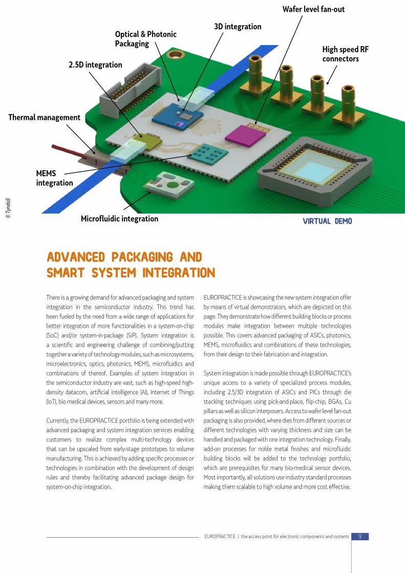
3D integration
2.5D integration
High speed RFconnectors
Wafer level fan-out
Microfluidic integration
Thermal management
MEMS integration
Optical & Photonic Packaging
ADVANCED PACKAGING AND SMART SYSTEM INTEGRATIONThere is a growing demand for advanced packaging and system
integration in the semiconductor industry. This trend has
been fueled by the need from a wide range of applications for
better integration of more functionalities in a system-on-chip
(SoC) and/or system-in-package (SiP). System integration is
a scientific and engineering challenge of combining/putting
together a variety of technology modules, such as microsystems,
microelectronics, optics, photonics, MEMS, microfluidics and
combinations of thereof. Examples of system integration in
the semiconductor industry are vast, such as high-speed high-
density datacom, artificial intelligence (AI), Internet of Things
(IoT), bio-medical devices, sensors and many more.
Currently, the EUROPRACTICE portfolio is being extended with
advanced packaging and system integration services enabling
customers to realize complex multi-technology devices
that can be upscaled from early-stage prototypes to volume
manufacturing. This is achieved by adding specific processes or
technologies in combination with the development of design
rules and thereby facilitating advanced package design for
system-on-chip integration.
EUROPRACTICE is showcasing the new system integration offer
by means of virtual demonstrators, which are depicted on this
page. They demonstrate how different building blocks or process
modules make integration between multiple technologies
possible. This covers advanced packaging of ASICs, photonics,
MEMS, microfluidics and combinations of these technologies,
from their design to their fabrication and integration.
System integration is made possible through EUROPRACTICE’s
unique access to a variety of specialized process modules,
including 2.5/3D integration of ASICs and PICs through die
stacking techniques using pick-and-place, flip-chip, BGAs, Cu
pillars as well as silicon interposers. Access to wafer level fan-out
packaging is also provided, where dies from different sources or
different technologies with varying thickness and size can be
handled and packaged with one integration technology. Finally,
add-on processes for noble metal finishes and microfluidic
building blocks will be added to the technology portfolio,
which are prerequisites for many bio-medical sensor devices.
Most importantly, all solutions use industry standard processes
making them scalable to high volume and more cost effective.
© T
ynda
ll
VIRTUAL DEMO
9EUROPRACTICE | the access point for electronic components and systems

FROM PROTOTYPES TO VOLUME PRODUCTIONAfter successful ASIC prototyping, we can also provide
customer access to the full production and qualification
stage (from low to mid-high volumes).
PROTOTYPE FABRICATION When all the checks have been performed, the ASIC can be
fabricated on one of the MPW’s or on a dedicated mask set.
EUROPRACTICE takes care of the production for the first
prototypes of the customer and organizes the assembly in ceramic
or plastic packages if required. Using their own bench tests, the
designer can check the functionality of the ASIC in an early stage.
DEVELOPMENT OF A TEST SOLUTION When the device behaves according to the ASIC specifications,
a test solution on an ATE (Automatic Test Equipment) platform
is required to deliver electrical screened devices using a volume
production test program. The test can be performed on both
wafer level and on packaged devices. The goal is to reduce the
test time and to examine the ASIC for manufacturing problems
using the ATPG (Automatic Test Pattern Generation) and
functional patterns. EUROPRACTICE supports you during the
development of single-site test solution as well as with a multi-
site test solution when high-volume testing is required. Based on
the test strategy, different solutions can be implemented.
DEBUG AND CHARACTERIZATION Before going into production, a characterization test program
checks if all the ASIC specifications meet the customer’s
expectations. Threshold values are defined for each tested
parameter. The software tests all the IP blocks and the results
are verified with the bench test results. A characterization at
Low (LT), Room (RT) and High (HT) temperature is performed
on a number of (corner) samples together with statistical
analysis (Cp and Cpk) to understand the sensitivity of the
design against corner process variations.
QUALIFICATION When the silicon is proven to be strong against process variations,
the product qualification can start. EUROPRACTICE can support
you through the full qualification process using different kind of
qualification flows, including Automotive, Consumer, Industrial,
Medical, Space, Military, Jedec and ESCC standards.
In this stage of the project, qualification boards must be
developed for reliability tests and environmental tests.
YIELD IMPROVEMENT EUROPRACTICE can perform yield analysis to determine
critical points during the production and suggest the correct
solution to maximize the yield. During the characterization
and qualification of the device on corner lots, EUROPRACTICE
can support the customer in defining the final parameter
windows. Depending on the device sensitivity to process
variations, the foundry will use the optimal process flow.
During the ramp-up phase, data of hundreds of wafers are
analyzed to check for yield issues related to assembly or
wafer production. EUROPRACTICE is using the well proven
tool Examinator™ from Galaxy Semiconductor that enables
our engineers to perform fast data and yield analysis studies.
SUPPLY CHAIN MANAGEMENT EUROPRACTICE is responsible for the full supply chain. This
highly responsive service takes care of allocating in the shortest
time the customer orders during engineering and production
phases. Integrated logistics is applied across the partners to
accurately achieve the final delivery dates.
Customer products are treated internally as projects and
followed closely by the EUROPRACTICE engineers. Our strong
partner’s relations empower us to deal with many of the changing
requests of our customers. EUROPRACTICE therefore acts as an
extension of the operational unit of the customers by providing
them a unique interface to the key required sub-contractors.
• Ceramic assembly partners: Alter Technology, Kyocera,
SERMA Microelectronics, Teledyne e2v
• Plastic assembly partners: Amkor Technology, ASE,
Greatek Electronics, Integra Technologies, Kyocera,
StatsChipPac
• Wafer bumping partners: ASE, FlipChip International,
Pactech
• Si-Photonics packaging: Alter Technology, PIXAPP, Tyndall
• Test partners: Alter Technology, Aptasic, ASE, Bluetest,
Delta, EAG Laboratories, Salland Engineering, Microtest,
RoodMicrotec
• Failure analysis: Maser Engineering, RoodMicrotec
• Library partners: Aragio, ARM, Cadence, eMemory, Faraday,
INVECAS, Synopsys
• Rad test facility: LLN, RADEF
• Tape & Reel: Reel Service
• Long-term storage: HTV
10 EUROPRACTICE | the access point for electronic components and systems
TRAINING IN DESIGN TOOLS AND TECHNOLOGIESEUROPRACTICE traditionally has organized high-quality
training courses in design tools and technologies. With the
beginning of the COVID-19 pandemic, these face-to-face
events had to be suspended as of March 2020. To remain
in close contact with existing customers and to introduce
EUROPRACTICE services to new potential users, highly
successful webinar series were organized.
TRAINING COURSESEUROPRACTICE provides training courses targeting academic
staff and PhD students from European universities and research
institutes. Unlike training courses which address single topics
or individual design tools, the EUROPRACTICE training courses
typically address a design flow which makes these training
courses an efficient way to acquire new knowledge and ideally
suited to new PhD students and junior engineers with a need to
quickly become productive with a design flow.
Since the courses are based on the EUROPRACTICE design
tools, PDKs and Technologies, participants will be able to
directly apply the techniques learnt on the training course
when they return back to their own organization and make full
use of the EUROPRACTICE infrastructure in their innovation,
research and training.
Courses include a strong element of practical sessions where
participants have an opportunity to extensively practice the
concepts described in lectures and have access to experts
who can answer questions about the concepts, design
tools or technology processes discussed on the course.
Where a design flow is well supported by multiple vendors
and/or processes, multiple course variants are offered that
reflect the typical practice within European industry.
Since EUROPRACTICE Training courses began in April 2014,
a total of 1285 delegates from 302 Member Institutes in
40 countries have attended 143 training courses making
4585 days of practical training.
Due to the COVID-19 pandemic, physical training courses
were suspended from March 2020 onwards. Therefore,
existing physical training courses were reconfigured
and adapted so they could be presented online as live
instructor-led training including (where appropriate) hands-
on practical sessions using remotely accessible design tool
environments. The consortium partners have also focused
on development of webinars.
© im
ec
11EUROPRACTICE | the access point for electronic components and systems
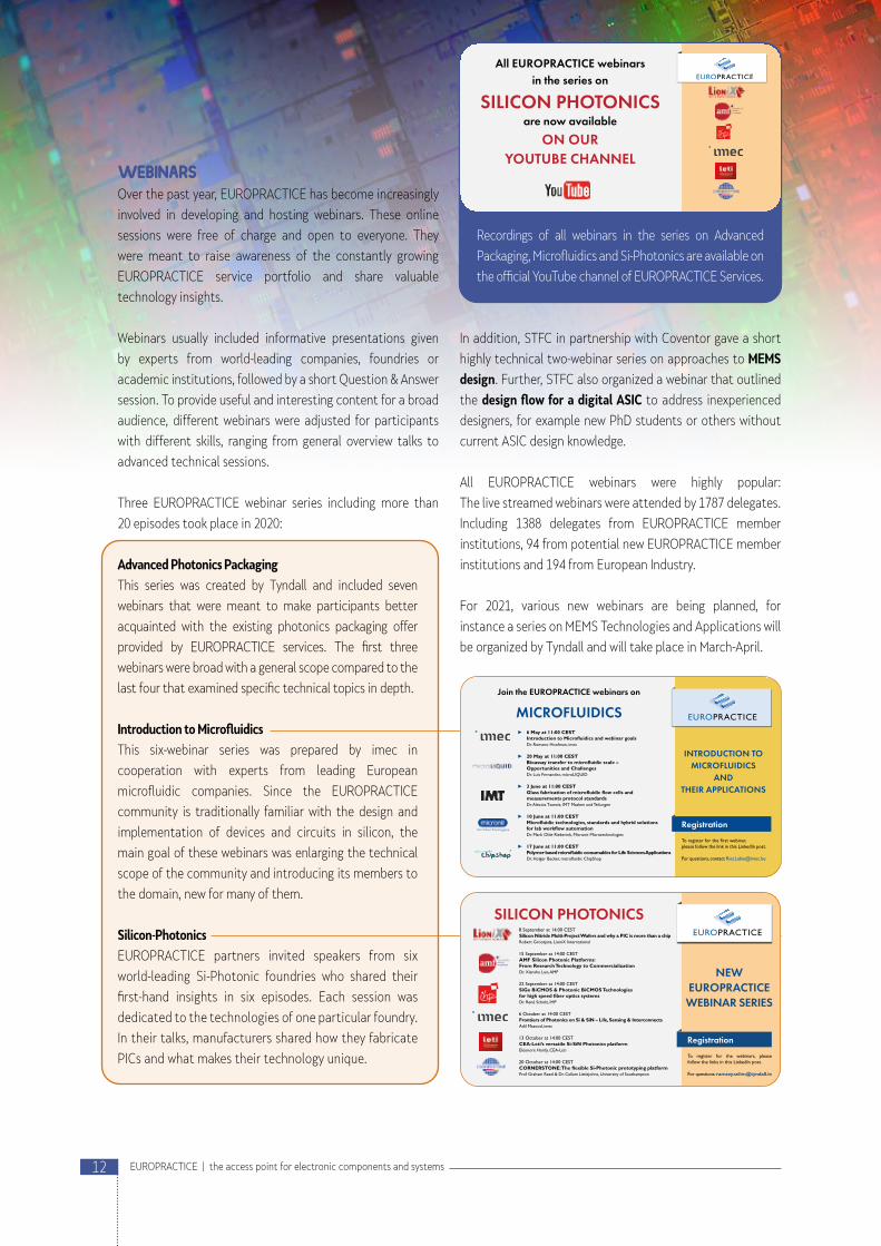
WEBINARSOver the past year, EUROPRACTICE has become increasingly
involved in developing and hosting webinars. These online
sessions were free of charge and open to everyone. They
were meant to raise awareness of the constantly growing
EUROPRACTICE service portfolio and share valuable
technology insights.
Webinars usually included informative presentations given
by experts from world-leading companies, foundries or
academic institutions, followed by a short Question & Answer
session. To provide useful and interesting content for a broad
audience, different webinars were adjusted for participants
with different skills, ranging from general overview talks to
advanced technical sessions.
Three EUROPRACTICE webinar series including more than
20 episodes took place in 2020:
Advanced Photonics Packaging
This series was created by Tyndall and included seven
webinars that were meant to make participants better
acquainted with the existing photonics packaging offer
provided by EUROPRACTICE services. The first three
webinars were broad with a general scope compared to the
last four that examined specific technical topics in depth.
Introduction to Microfluidics
This six-webinar series was prepared by imec in
cooperation with experts from leading European
microfluidic companies. Since the EUROPRACTICE
community is traditionally familiar with the design and
implementation of devices and circuits in silicon, the
main goal of these webinars was enlarging the technical
scope of the community and introducing its members to
the domain, new for many of them.
Silicon-Photonics
EUROPRACTICE partners invited speakers from six
world-leading Si-Photonic foundries who shared their
first-hand insights in six episodes. Each session was
dedicated to the technologies of one particular foundry.
In their talks, manufacturers shared how they fabricate
PICs and what makes their technology unique.
Recordings of all webinars in the series on Advanced
Packaging, Microfluidics and Si-Photonics are available on
the official YouTube channel of EUROPRACTICE Services.
All EUROPRACTICE webinarsin the series on
SILICON PHOTONICSare now available
ON OURYOUTUBE CHANNEL
In addition, STFC in partnership with Coventor gave a short
highly technical two-webinar series on approaches to MEMS
design. Further, STFC also organized a webinar that outlined
the design flow for a digital ASIC to address inexperienced
designers, for example new PhD students or others without
current ASIC design knowledge.
All EUROPRACTICE webinars were highly popular:
The live streamed webinars were attended by 1787 delegates.
Including 1388 delegates from EUROPRACTICE member
institutions, 94 from potential new EUROPRACTICE member
institutions and 194 from European Industry.
For 2021, various new webinars are being planned, for
instance a series on MEMS Technologies and Applications will
be organized by Tyndall and will take place in March-April.
SILICON PHOTONICS8 September at 14:00 CESTSilicon Nitride Multi-Project Wafers and why a PIC is more than a chipRobert Grootjans, LioniX International
15 September at 14:00 CESTAMF Silicon Photonic Platforms:From Research Technology to CommercializationDr. Xianshu Luo, AMF
22 September at 14:00 CESTSiGe BiCMOS & Photonic BiCMOS Technologies for high speed fiber optics systemsDr. René Scholz, IHP
6 October at 14:00 CESTFrontiers of Photonics on Si & SiN – Life, Sensing & InterconnectsAdil Masood, imec
13 October at 14:00 CESTCEA-Leti’s versatile Si-SiN Photonics platformEléonore Hardy, CEA-Leti
20 October at 14:00 CESTCORNERSTONE: The flexible Si-Photonic prototyping platform Prof Graham Reed & Dr. Callum Littlejohns, University of Southampton
NEW EUROPRACTICE
WEBINAR SERIES
Registration
To register for the webinars, please follow the links in this LinkedIn post.
For questions: [email protected]
Join the EUROPRACTICE webinars on
MICROFLUIDICS 6 May at 11:00 CEST
Introduction to Microfluidics and webinar goalsDr. Romano Hoofman, imec
20 May at 11:00 CESTBioassay transfer to microfluidic scale – Opportunities and ChallengesDr. Luis Fernandez, microLIQUID
3 June at 11:00 CESTGlass fabrication of microfluidic flow cells and measurements protocol standardsDr. Alexios Tzannis, IMT Masken und Teilungen
10 June at 11:00 CESTMicrofluidic technologies, standards and hybrid solutions for lab workflow automationDr. Mark Olde Riekerink, Micronit Microtechnologies
17 June at 11:00 CESTPolymer based microfluidic consumables for Life Sciences ApplicationsDr. Holger Becker, microfluidic ChipShop
INTRODUCTION TO MICROFLUIDICS
AND THEIR APPLICATIONS
Registration
To register for the first webinar,please follow the link in this LinkedIn post.
For questions, contact [email protected]
12 EUROPRACTICE | the access point for electronic components and systems
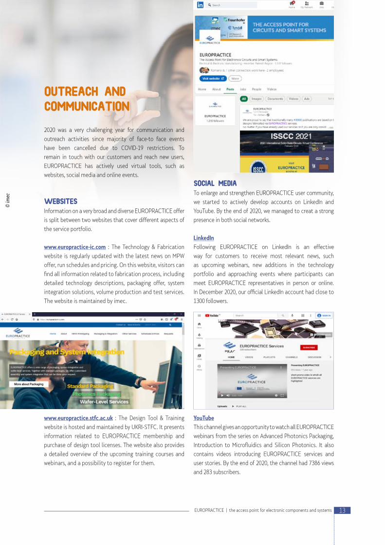
SOCIAL MEDIATo enlarge and strengthen EUROPRACTICE user community,
we started to actively develop accounts on LinkedIn and
YouTube. By the end of 2020, we managed to creat a strong
presence in both social networks.
Following EUROPRACTICE on LinkedIn is an effective
way for customers to receive most relevant news, such
as upcoming webinars, new additions in the technology
portfolio and approaching events where participants can
meet EUROPRACTICE representatives in person or online.
In December 2020, our official LinkedIn account had close to
1300 followers.
YouTube
This channel gives an opportunity to watch all EUROPRACTICE
webinars from the series on Advanced Photonics Packaging,
Introduction to Microfluidics and Silicon Photonics. It also
contains videos introducing EUROPRACTICE services and
user stories. By the end of 2020, the channel had 7386 views
and 283 subscribers.
OUTREACH AND COMMUNICATION2020 was a very challenging year for communication and
outreach activities since majority of face-to face events
have been cancelled due to COVID-19 restrictions. To
remain in touch with our customers and reach new users,
EUROPRACTICE has actively used virtual tools, such as
websites, social media and online events.
WEBSITESInformation on a very broad and diverse EUROPRACTICE offer
is split between two websites that cover different aspects of
the service portfolio.
www.europractice-ic.com : The Technology & Fabrication
website is regularly updated with the latest news on MPW
offer, run schedules and pricing. On this website, visitors can
find all information related to fabrication process, including
detailed technology descriptions, packaging offer, system
integration solutions, volume production and test services.
The website is maintained by imec.
www.europractice.stfc.ac.uk : The Design Tool & Training
website is hosted and maintained by UKRI-STFC. It presents
information related to EUROPRACTICE membership and
purchase of design tool licenses. The website also provides
a detailed overview of the upcoming training courses and
webinars, and a possibility to register for them.
© im
ec
13EUROPRACTICE | the access point for electronic components and systems

EVENTS IN TIMES OF COVID-19 Every year, EUROPRACTICE is present at
various scientific conferences, industrial
trade shows and fairs in order to present
its services to existing customers and
to attract new prospects. Although
physical events planned for 2020 have
been cancelled from March onward
due to the COVID-19 outbreak, multiple
event organizers have turned to a virtual
format.
During last year, EUROPRACTICE
participated in several online events
with virtual booths, posters and flyers
that were developed specifically for
these purposes. However, networking
and direct interaction with customers
remained difficult. As a result, no
National Seminars took place in 2020
because active face-to-face networking
is their core purpose.
To compensate for the lack of physical
outreach and communication
opportunities, EUROPRACTICE has been
successfully using online communication
by means of webinars and social media.
In 2021, we are planning to remain
in close contact with our customers
and prospects. To achieve this, we will
keep hosting virtual events, such as
new webinar series and an upcoming
industry-cluster event co-organized with
DSP Valley. In addition, we will attend at
least the following conferences and fairs:
ISSCC 2021 Virtual event 13-22 February
SSI 2021 Virtual event 27-29 April
TRANSDUCERS 2021 Virtual event 20-25 June
PRIME 2021 Virtual event 19-22 July
ESSDERC / ESSCIRC2021 Grenoble, France 6-9 September
EFECS 2021 Amsterdam, the Netherlands 23-25 November
EUROPRACTICE team at MEMS2020 in Vancouver.
EUROPRACTICE poster for virtual events.
LinkedIn invitation to visit virtual EUROPRACTICE booth at EFECS2020.
© im
ec
14 EUROPRACTICE | the access point for electronic components and systems

RESULTS 2020: MPW PROTOTYPING SERVICES
MPW designs in 2020
Industry outside Europe 4%
European research institutes 21%
European universities 39%Research outside Europe 16%
European industry 20%
Number of fabricated designs in 2020 per foundry
ams, 77 AMF, 1
EMM, 1CEA-Leti, 8
GLOBALFOUNDRIES, 45
IHP, 67
imec, 43
MEMSCAP, 8
ON Semiconductor, 18
TSMC, 388
STMicroelectronics , 99
UMC, 93X-FAB, 48
PROTOTYPED CIRCUITS ON MPW RUNSIn 2020, a total of 896 design projects
have been submitted for prototyping
on EUROPRACTICE MPW runs. This
number is slightly higher than for the
previous year, which is remarkable for
such an unusually difficult year as 2020.
It demonstrates that research and
innovation could continue at the same
pace and EUROPRACTICE together with
its foundry partners continued to support
its customers despite the COVID-19
restrictions.
ACCESS TO TECHNOLOGIES OF WORLD-LEADING FOUNDRIESEUROPRACTICE provides affordable access to technologies
of world-leading foundries (ams, GLOBALFOUNDRIES, ON
Semiconductor, STMicroelectronics, TSMC, UMC and X-FAB),
complemented by specialty fabs at CEA-Leti, IHP, imec and
MEMSCAP. This year, the first design projects were submitted
in AMF and EM Microelectronic technologies. Similar to last
year, most of the submitted designs in 2020 were fabricated in
TSMC, which is also the leading foundry for the global industry.
Remarkably, two of the European foundries –
STMicroelectronics and austriamicrosystems (ams) – have
the second and fourth largest number of designs fabricated.
One of the other European foundries, X FAB, has increased
its number of fabricated designs once again as compared to
last year(s).
60% of the prototypes were designed by European universities and research institutes, while 20% of the designs are coming
from European industry (mainly SMEs). The remaining 20% of the designs are coming from outside Europe, namely 16% from
research institutions and 4% from industry.
15EUROPRACTICE | fabricated designs in 2020

GOOD TECHNOLOGY MIXEUROPRACTICE offers a good
technology mix to its customers.
Advanced technologies, older
technology nodes and More-
than-Moore technologies are all
used in significant volume by the
EUROPRACTICE customers. The
older technology nodes (ranging
from 0.11μm to 0.8μm) are still very
popular and represent approximately
half of the total designs submitted.
For the more advanced nodes, 65nm
and associated nodes are the most
popular with 181 fabricated designs.
In addition, the 28nm technology node
is used very frequently by the customers
and its share has significantly grown
compared to last year. 33 designs in
total were realized in 22nm nodes.
The 22nm FDSOI technology from
GLOBALFOUNDRIES has once again
shown tremendous growth in the
number of designs, as it has more than
doubled the figures: from 15 last year to
33 this year. The access to 16nm FinFET
technology from TSMC can only be
offered to a restricted set of customers,
reflected by only 3 prototypes in 2020.
The number of designs in Silicon
Photonics technologies has mildly
decreased due to a reduced number
of designs in the imec Si-Photonics
technologies in the first half of the year.
It seems that those technologies were
the only ones who saw an impact of
the COVID-19 pandemic. The number
of MEMS designs has slightly increased
thanks to the X FAB XMB10 design
competition. Finally, 2 designs have been
fabricated in the GaN-IC technology,
which was added only last year to the
EUROPRACTICE technology portfolio.
Number of fabricated designs in 2020 per technology (node)
Si-Photonics, 4616nm, 3
28nm, 10822nm, 33
MEMS, 11
GaN, 2 0.8µ...5µ, 7
0.35µ, 910.25µ, 4
0.18µ...0.15µ, 211
0.13µ...0.11µ, 15390nm, 1
65...55nm, 181
45...40nm, 45
GEOGRAPHICAL DISTRIBUTIONAlthough EUROPRACTICE focuses
mainly on European customers,
its services are also accessible for
customers outside Europe. 64% of the
fabricated designs are coming from
the European Union and another 16%
from other countries in the EMEA
(Europe, Middle East and Africa) zone.
A significant number of customers from
Asia are also using the EUROPRACTICE
prototyping services – representing
a total volume of 97 designs in 2020.
Finally, the remaining 9% of the
designs fabricated are coming from the
Americas and the Australian continent. Geographical distribution of MPW designs in 2020
Australia, 0.4%
Rest of EMEA, 16.2%
Asia, 10.8%
Americas, 8.8%
EU, 63.7%
16 EUROPRACTICE | fabricated designs in 2020
0 20 40 60 80 100 120 140
Australia
Austria
Belgium
Brazil
Canada
China + HK + Macau
Czech Republic
Denmark
Egypt
Finland
France
Germany
Greece
India
Ireland
Israel
Italy
Japan
Korea, Republic
Latvia
Malaysia
Malta
Mexico
Netherlands
New Zealand
Norway
Philippines
Poland
Portugal
Russia
Singapore
Slovakia
Slovenia
South Africa
Spain
Sweden
Switzerland
Taiwan
Thailand
Turkey
United Kingdom
Uruguay
USA
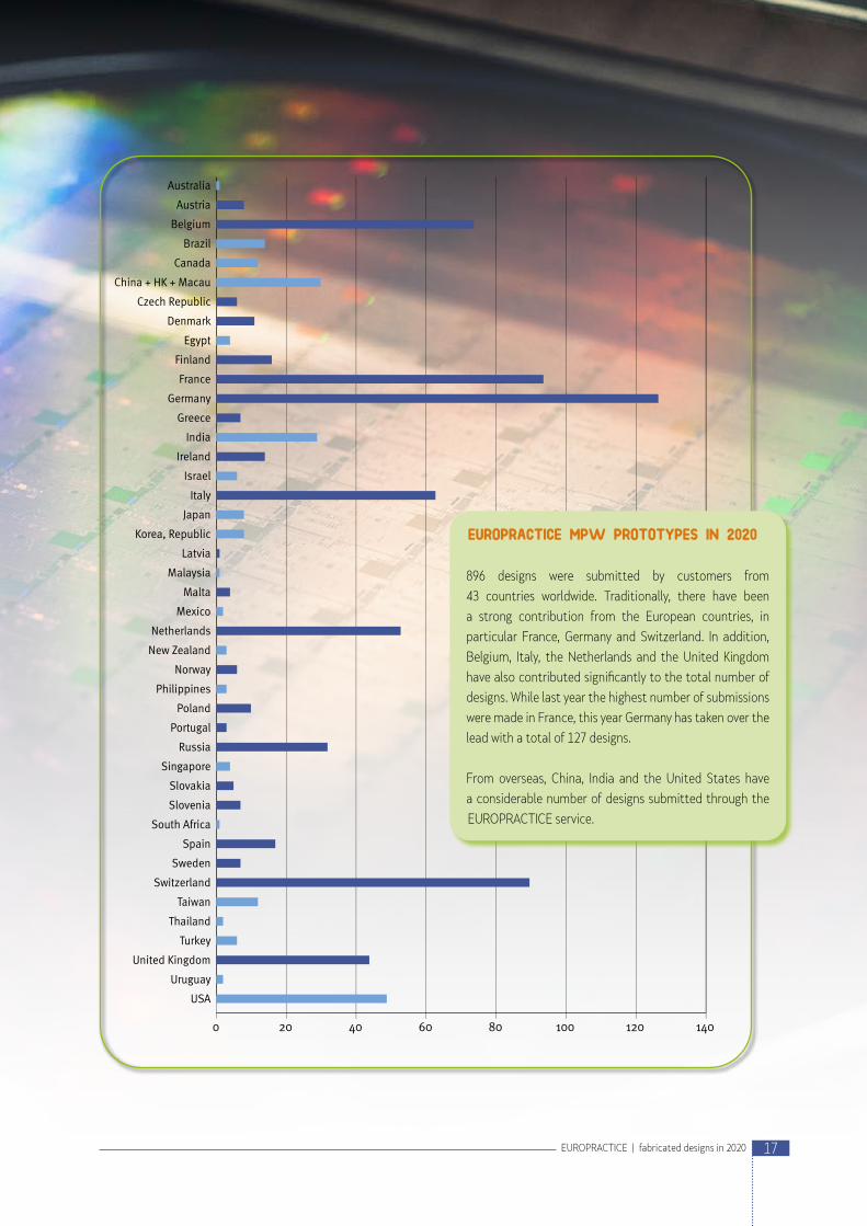
EUROPRACTICE MPW PROTOTYPES IN 2020
896 designs were submitted by customers from
43 countries worldwide. Traditionally, there have been
a strong contribution from the European countries, in
particular France, Germany and Switzerland. In addition,
Belgium, Italy, the Netherlands and the United Kingdom
have also contributed significantly to the total number of
designs. While last year the highest number of submissions
were made in France, this year Germany has taken over the
lead with a total of 127 designs.
From overseas, China, India and the United States have
a considerable number of designs submitted through the
EUROPRACTICE service.
17EUROPRACTICE | fabricated designs in 2020

USER STORIES ON PROTOTYPED DESIGNS
© im
ec
18 EUROPRACTICE | user stories on prototyped designs

ams S35
Warm front-end for X-ray cryogenic detectorsAPC Laboratory, Paris, France
Contacts: Damien Prêle, Si Chen
E-mail: [email protected]
Technology: ams SiGe BiCMOS 0.35μm S35D4M5
Die size: 26.146 mm2
IntroductionAwaXe_v3 (Athena Warm Asic for the X-ifu Electronics
- version 3) is an upgrade ASIC developed for the Warm
Front End Electronics (WFEE) of a future X-ray observatory:
ATHENA, a space mission of ESA.
It is dedicated to an early demonstration model (Phase B) to
validate the Time-Division Multiplexing (TDM) readout of the
X-IFU (X-ray Integral Field Unit) instrument of the ATHENA
telescope. It includes two TDM channels for low noise
amplification and the bias of the TES/SQUID cryogenic
detection chain.
This ASIC belongs to the “AwaXe and SQmux ASIC families”
developed at APC Laboratory for SQUID/TES readout.
The development is funded by CNES and CNRS.
DescriptionAwaXe_v3 integrates two TDM readout channels of the
X-IFU instrument. It is a mixed ASIC, mainly composed of:
• 2 identical fully-differential Low Noise Amplifiers
(1/ CH) to amplify scientific signals, with proper voltage
gain ≈ 170 V/V, bandwidth (-3 dB) ≈24 MHz, ultra-low
equivalent input noise < 1 nV/√Hz, low non-linearity <1%
and low gain drift < 350 ppm/K in the range of [11°C,
75°C]. Input and output impedance matching is also
practicable;
• 10 differential configurable current sources for the bias
of SQUIDs and TES (5/CH), with maximum output 3.6 mA
or 600 μA. 4 of the 10 sources further respectively have
an attached fixed current source (2/CH), allowing to
have an alternative bias range of [-1.8 mA, 1.8 mA] or
[-300 μA, 300 μA]. Current noise has been optimised
down to low frequencies (1-100 Hz);
• A digital RadHard series bus RS485/I2C of 8-bit for the
slow control of all 10 configurable current sources;
• Housekeeping elements to monitor temperature,
current and voltage of the ASIC;
• 6 heating modules (3/CH) with nominal output 18 mA
to heat/deflux cryogenic devices.
Fig.1: Layout of the circuit.
19EUROPRACTICE | user stories on prototyped designs

GLOBALFOUNDRIES 22FDX
Sub 30 GHz VCOs in 22nm FDSOI for radar and communication applicationsInstitut für Mikroelektronik und Schaltungstechnik, Universität der Bundeswehr München, Germany
Contacts: MSc. Piyush Kumar, Dipl.-Ing Dario Stajic, Prof. Linus Maurer
E-mail: [email protected]
Technology: GLOBALFOUNDRIES 22nm FD-SOI 22FDX
Die size: VCO in mm-Wave Spectrum: 345µm × 446µm;
push VCO: 448µm × 652µm
Design tools: Cadence IC advance, Mentor Calibre (for DRC, LVS,
XACT checks), ADS-Momentum for the EM simulation of the coil
IntroductionOcean 12 is an ECSEL co-funded project which is an Opportunity
to Carry European Autonomous driving further with FDSOI
technology. Based on the innovative FDSOI technology to
develop new processors and applications design that leverage
Fully Depleted Silicon On Insulator (FD-SOI) technology to offer
the industry’s lowest power integrated circuits, especially for
automotive and aeronautic applications.
The Institute for Microelectronic and Integrated Circuit (EIT4)
at Universität Der Bundeswehr, München (UniBwM), is focused
on realizing the building blocks for the frequency generation
of mm-Wave FMCW radars.
The activities of UniBwM are focused on novel VCO
architectures to be integrated with the Frequency Multipliers
to efficiently generate signals in the 76 to 81GHz signal band
used for automotive radar.
DescriptionAfter the successful tapeouts in 2018 and 2019, this year
Universität Der Bundeswehr participated in the MPW
tapeout from the EUROPRACTICE. We designed stand-alone
VCOs and Frequency Multipliers.
The VCOs are based on the modified Collpits-Oscillator and
push-push topology. The silicon is verified by wafer-prober
measurements and is fully functional.
The UniBwM designed a push-push VCO with the central
frequency of 20 GHz. This architecture was chosen as the
2nd harmonic can be further multiplied to the target frequency
band. The characterization of this block is in progress.
Why EUROPRACTICE?EUROPRACTICE offers prototype services and testing for state-
of-the-art technologies with mature PDKs at reasonable prices,
including modern nanometer scale processes such as GF22FDX,
which is used in this project. Without these services we as a
University could not participate in such design-centric projects.
They also provide excellent support for PDKs and tape-out
procedures till the GDS submission.
AcknowledgmentThis work was supported through OCEAN12 (Grant Nr 783127)
project, receiving funding from H2020 ECSEL JU program and
German Bundesministerium fur Bildung und Forschung (BMBF).
Fig.1: Design block.
Fig.4: Die Photo and Layout of the Push-Push VCO.
Fig.3: Die Photo and Layout of VCO in mm-Wave Spectrum.
Fig.2: Monte-Carlo analysis to estimate the variation in the Phase noise. of VCO.
Design block
RF_OUTBufferX4/X3VCO
20 EUROPRACTICE | user stories on prototyped designs

A D-band Differential Transmission Line Based Power CombinerSilicon Austria Labs, Linz, Austria
Contacts: Abouzar Hamidipour, Gernot Hueber
E-mail: [email protected]
Technology: GLOBALFOUNDRIES 22nm FD-SOI 22FDX
Die size: 1250μm × 1250μm
Design tools: EMX for EM simulations, Spectre for circuit
simulations, Calibre for fill generation and merging GDSII
files, PVS for DRC/LVS check
DescriptionWith the growing attention to 6G and frequencies beyond
100 GHz, many attempts are being made to explore
novel power combining structures. This is to overcome
technology limitations in providing conventionally high
output power. Traditional approaches of power combining
such as Wilkinson or transformer-based have been widely
used in lower frequency ranges as their theory is very well-
known and their design procedure is straightforward. In
frequencies beyond 100 GHz, however, transmission-line
based power combiners could be preferred as their size
shrinks appreciably and they prove comparatively low
insertion loss. To this end, a D-band differential power
combiner with 1:1 impedance ratio was designed based
on transmission lines in GLOBALFOUNDRIES 22nm FDSOI
technology. Transmission lines provide 50 Ω impedance
both at the input and the output of the combiner. Figure 1
shows a micrograph of the die and the test structure used to
verify insertion loss of the combiner. Impedance matching
was accomplished using quarter-wavelength transformers.
To fulfill low-characteristic impedance requirements, the
signal and ground traces of the strip lines were designed on
QA and M1 layers, respectively. As can be seen in Figure 2, a
very good agreement was achieved between the simulation
and measurement over the whole D-band frequency range.
Why EUROPRACTICE?EUROPRACTICE provides access to various state-of-the-art
technologies at affordable price. Furthermore, EUROPRACTICE
staff provide a very good customer service and technical
support. The variety of technologies and the frequency of runs
create a platform for excellent research opportunities.
Fig. 1: Microphotograph of the test structure used to verify the D-band differential power combiner.
Fig. 2: Measured and simulated S-parameters of the D-band differential power combiner.
GLOBALFOUNDRIES 22FDX
21EUROPRACTICE | user stories on prototyped designs
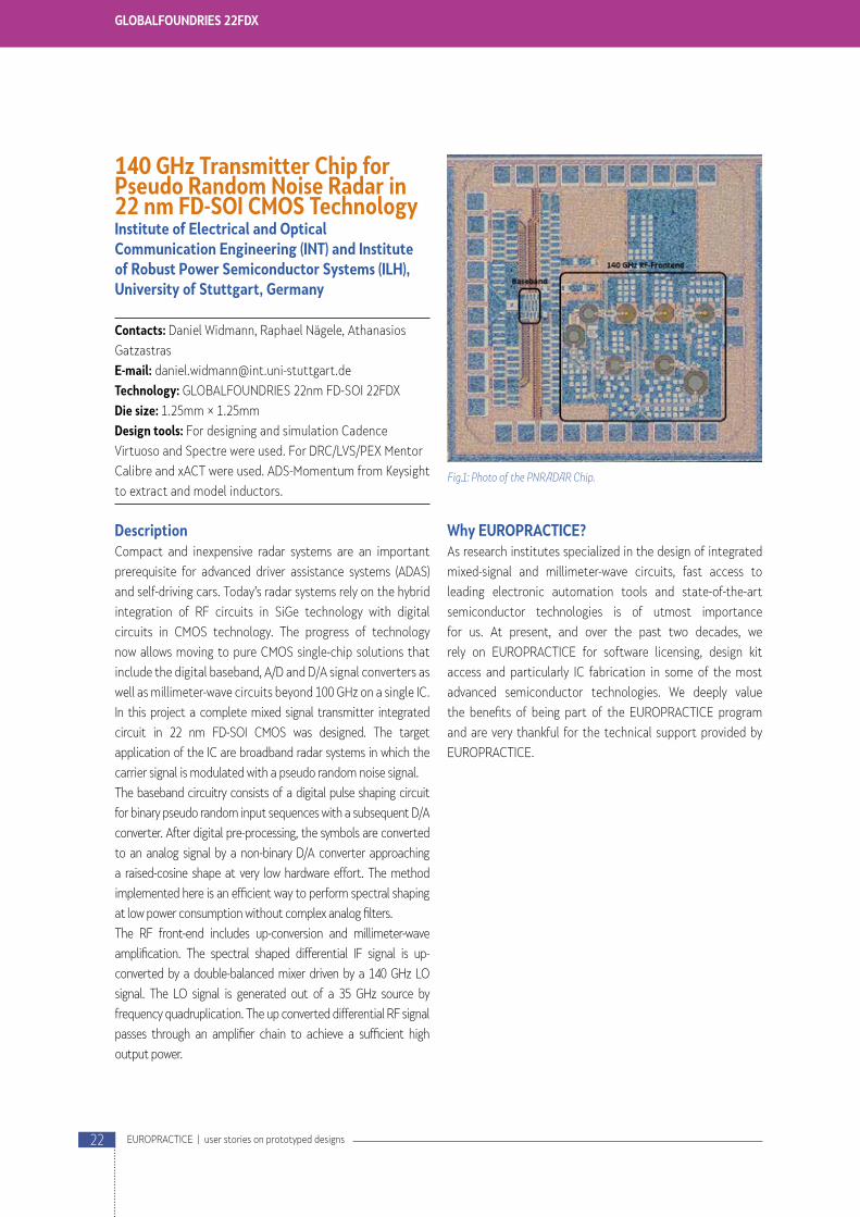
140 GHz Transmitter Chip for Pseudo Random Noise Radar in 22 nm FD-SOI CMOS Technology Institute of Electrical and Optical Communication Engineering (INT) and Institute of Robust Power Semiconductor Systems (ILH), University of Stuttgart, Germany
Contacts: Daniel Widmann, Raphael Nägele, Athanasios
Gatzastras
E-mail: [email protected]
Technology: GLOBALFOUNDRIES 22nm FD-SOI 22FDX
Die size: 1.25mm × 1.25mm
Design tools: For designing and simulation Cadence
Virtuoso and Spectre were used. For DRC/LVS/PEX Mentor
Calibre and xACT were used. ADS-Momentum from Keysight
to extract and model inductors.
Description Compact and inexpensive radar systems are an important
prerequisite for advanced driver assistance systems (ADAS)
and self-driving cars. Today’s radar systems rely on the hybrid
integration of RF circuits in SiGe technology with digital
circuits in CMOS technology. The progress of technology
now allows moving to pure CMOS single-chip solutions that
include the digital baseband, A/D and D/A signal converters as
well as millimeter-wave circuits beyond 100 GHz on a single IC.
In this project a complete mixed signal transmitter integrated
circuit in 22 nm FD-SOI CMOS was designed. The target
application of the IC are broadband radar systems in which the
carrier signal is modulated with a pseudo random noise signal.
The baseband circuitry consists of a digital pulse shaping circuit
for binary pseudo random input sequences with a subsequent D/A
converter. After digital pre-processing, the symbols are converted
to an analog signal by a non-binary D/A converter approaching
a raised-cosine shape at very low hardware effort. The method
implemented here is an efficient way to perform spectral shaping
at low power consumption without complex analog filters.
The RF front-end includes up-conversion and millimeter-wave
amplification. The spectral shaped differential IF signal is up-
converted by a double-balanced mixer driven by a 140 GHz LO
signal. The LO signal is generated out of a 35 GHz source by
frequency quadruplication. The up converted differential RF signal
passes through an amplifier chain to achieve a sufficient high
output power.
Fig.1: Photo of the PNRADAR Chip.
Why EUROPRACTICE? As research institutes specialized in the design of integrated
mixed-signal and millimeter-wave circuits, fast access to
leading electronic automation tools and state-of-the-art
semiconductor technologies is of utmost importance
for us. At present, and over the past two decades, we
rely on EUROPRACTICE for software licensing, design kit
access and particularly IC fabrication in some of the most
advanced semiconductor technologies. We deeply value
the benefits of being part of the EUROPRACTICE program
and are very thankful for the technical support provided by
EUROPRACTICE.
GLOBALFOUNDRIES 22FDX
22 EUROPRACTICE | user stories on prototyped designs
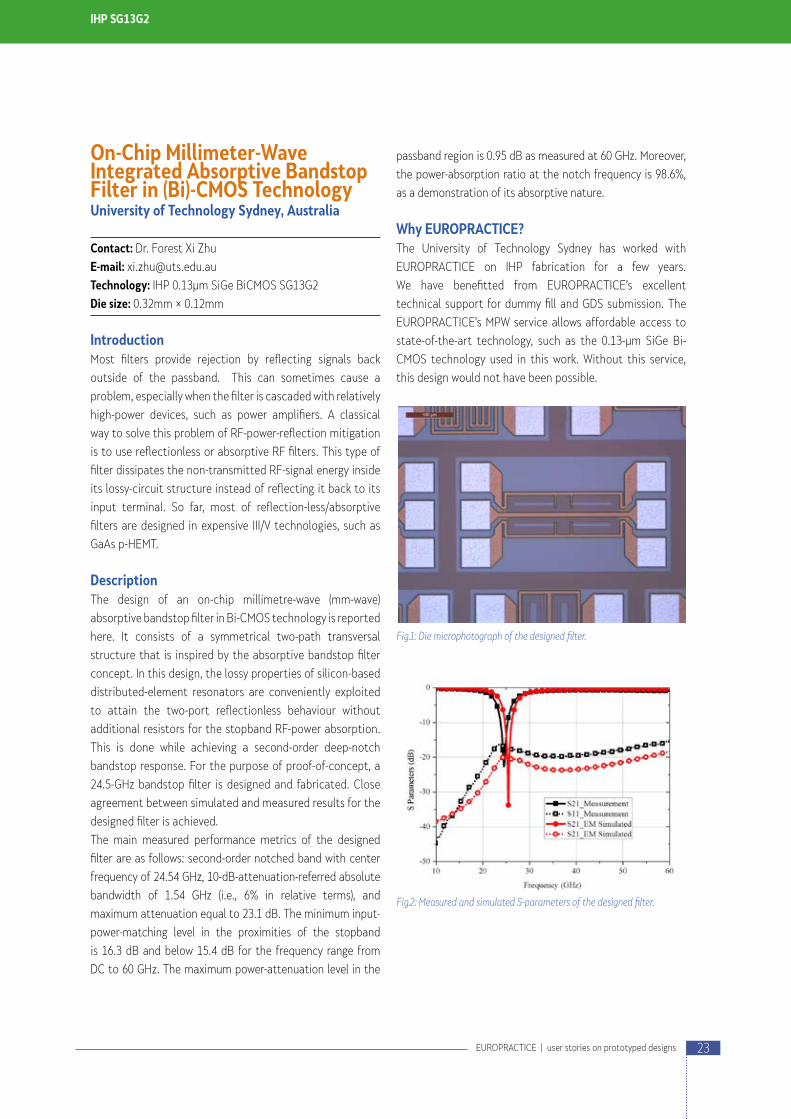
On-Chip Millimeter-Wave Integrated Absorptive Bandstop Filter in (Bi)-CMOS TechnologyUniversity of Technology Sydney, Australia
Contact: Dr. Forest Xi Zhu
E-mail: [email protected]
Technology: IHP 0.13μm SiGe BiCMOS SG13G2
Die size: 0.32mm × 0.12mm
IntroductionMost filters provide rejection by reflecting signals back
outside of the passband. This can sometimes cause a
problem, especially when the filter is cascaded with relatively
high-power devices, such as power amplifiers. A classical
way to solve this problem of RF-power-reflection mitigation
is to use reflectionless or absorptive RF filters. This type of
filter dissipates the non-transmitted RF-signal energy inside
its lossy-circuit structure instead of reflecting it back to its
input terminal. So far, most of reflection-less/absorptive
filters are designed in expensive III/V technologies, such as
GaAs p-HEMT.
DescriptionThe design of an on-chip millimetre-wave (mm-wave)
absorptive bandstop filter in Bi-CMOS technology is reported
here. It consists of a symmetrical two-path transversal
structure that is inspired by the absorptive bandstop filter
concept. In this design, the lossy properties of silicon-based
distributed-element resonators are conveniently exploited
to attain the two-port reflectionless behaviour without
additional resistors for the stopband RF-power absorption.
This is done while achieving a second-order deep-notch
bandstop response. For the purpose of proof-of-concept, a
24.5-GHz bandstop filter is designed and fabricated. Close
agreement between simulated and measured results for the
designed filter is achieved.
The main measured performance metrics of the designed
filter are as follows: second-order notched band with center
frequency of 24.54 GHz, 10-dB-attenuation-referred absolute
bandwidth of 1.54 GHz (i.e., 6% in relative terms), and
maximum attenuation equal to 23.1 dB. The minimum input-
power-matching level in the proximities of the stopband
is 16.3 dB and below 15.4 dB for the frequency range from
DC to 60 GHz. The maximum power-attenuation level in the
passband region is 0.95 dB as measured at 60 GHz. Moreover,
the power-absorption ratio at the notch frequency is 98.6%,
as a demonstration of its absorptive nature.
Why EUROPRACTICE?The University of Technology Sydney has worked with
EUROPRACTICE on IHP fabrication for a few years.
We have benefitted from EUROPRACTICE’s excellent
technical support for dummy fill and GDS submission. The
EUROPRACTICE’s MPW service allows affordable access to
state-of-the-art technology, such as the 0.13-μm SiGe Bi-
CMOS technology used in this work. Without this service,
this design would not have been possible.
Fig.1: Die microphotograph of the designed filter.
Fig.2: Measured and simulated S-parameters of the designed filter.
IHP SG13G2
23EUROPRACTICE | user stories on prototyped designs

Silicon-Based IC-Waveguide Integration for High-Efficiency and Compact Millimeter-Wave Spatial Power CombinerIntegrated Circuits (IC) and Electromagnetics (EM) Group, Eindhoven University of Technology, The Netherlands
Contacts: Piyush Kaul, Alhassan Aljarosha
E-mail: [email protected]
Technology: IHP 0.13μm SiGe BiCMOS SG13S
Die size: 1.18mm × 0.86mm
Design Tools: Cadence: SPECTRE, IC and ASSURA
DescriptionModern wireless systems operating at Millimeter-wave (mm-wave)
frequencies require a low-loss packaging solution with a compact
system-level integration. The research on such systems at mm-
wave frequencies is focused on developing efficient power-
generating systems based on III-V technology. However, in the past
decade, silicon-based technology has rapidly gained significant
interest as an alternative solution for the development of such
systems. The high-level of integration of several transceiver
blocks and size-scaling trend of the technology enable it to be
more promising for high-volume commercial applications. In
silicon-based wireless systems, the achievable output power is
limited at mm-wave frequencies from a single amplifier. However,
number of amplifiers that can be combined to achieve high
output power is limited due to a trade-off between number of
combiner ports and combiner insertion loss.
Packaging using RF interconnects such as flip-chip
technology or bond-wires from MMICs to waveguides or high
gain antennas introduces more insertion losses in addition to
power-combiner loss, which is another challenge at Millimeter-
wave frequencies. Moreover, the manufacturing and assembly
process of waveguides at these frequencies is difficult in
terms of accuracy and tolerances. Therefore, realization of a
galvanic contact remains a challenge for transfer of signals
between MMICs and waveguides at mm-wave frequencies.
The purpose of this IC-Waveguide system is to present a new
packaging solution providing a contactless, and low-loss IC-
to-waveguide connection [1]. The proposed solution considers
a p-doped lossy substrate silicon-IC-to-waveguide connection
for the first time. The silicon-IC comprising an array of coupling
pads and microstrip lines is implemented in back-end-of-line
(BEoL) of IHP Microelectronics SiGe BiCMOS process, SG13S.
The RF-signals are directly coupled from the MMIC coupling-
pads to a ridge waveguide via a cavity resonator, which
enables a low-loss spatial power combiner in air.
Figure 1 presents the 3D model of the IC-Waveguide system.
Figure 2 presents the passive back-to-back IC structure
consisting of coupling pads and microstrip lines. The IC structure
also uses the TSV module for enhanced RF performance.
Why EUROPRACTICE?Eindhoven University of Technology has been a frequent user
of EUROPRACTICE’s project runs. EUROPRACTICE services
provide access to several advanced technology nodes.
They also provide access to design support, process design
kits, knowledge transfers, and design software (Cadence:
SPECTRE, IC and ASSURA) in addition to design runs.
References[1] P. Kaul, A. Aljarosha, A. B. Smolders, P.G.M. Baltus, M. Matters-Kam-
merer and R. Maaskant, “An E-Band Silicon-IC-to-Waveguide Contact-
less Transition Incorporating a Low-Loss Spatial Power Combiner,”
2018 Asia-Pacific Microwave Conference (APMC), Kyoto, 2018, pp. 1528-
1530, doi: 10.23919/APMC.2018.8617206.
IHP SG13S
Fig.1: Schematic representation of the building blocks of the device.
Fig.2: Photograph of the fabricated die.
24 EUROPRACTICE | user stories on prototyped designs

BrainWave: Ultra-Low-Power ProcessorEindhoven University of Technology, Eindhoven, The Netherlands
Contact: Kamlesh Singh
E-mail: [email protected]
Technology: ST 28nm FD-SOI CMOS
Die size: 1.49 mm2
IntroductionThe BrainWave processor aims for real-time epileptic seizure
detection and classification. The chip is an ultra-low-power
advanced digital signal processing SoC consisting of a
RISC-V core and a coarse-grained reconfigurable accelerator
(CGRA).
DescriptionThe SoC implementation is a voltage converter
free design based on three-level voltage stack
operating using a single voltage source of 1.8V.
The current consumption of SRAMs in the top
stack is recycled to sustain the near/sub-threshold
operation of logic circuits in the two lower stacks.
The chip achieves up to 95% power delivery efficiency with a
negligible area overhead. The energy efficiency achieved at
near/sub-threshold operation (0.4V) is 35MMACs/mW with a
peak performance of 4MMAC/s.
ROSQUILLAS: Ring Oscillators array to measure RTNHiPICS research group, Electronic Engineering Dept., Universitat Politècnica de Catalunya-BarcelonaTech (UPC), Barcelona, Spain
Contact: Enrique Barajas
E-mail: [email protected]
Technology: ST 28nm FD-SOI CMOS
Die size: 1.16 mm2
IntroductionThis chip has been fabricated to analyze the effect of
Random Telegraph Noise (RTN) in circuits fabricated with this
technology and used in very low power supply environments.
STMicroelectronics 28FDSOI STMicroelectronics 28FDSOI
Fig.1
: Bra
inW
ave
layo
ut.
Fig.1
: Lay
out o
f the
circ
uit.
Fig.2: Voltage output as a function of time for one of the oscillators.
25EUROPRACTICE | user stories on prototyped designs

Fig1
: Pho
togr
aph
of th
e fa
bric
ated
die
.Fi
g2: T
est r
esul
ts o
f the
MM
WTA
GIQ
dev
ice.
W-Band Active Mirror for OFDM RadarUniversity of Toronto, Canada
Contact: Sadegh Dadash
E-mail: [email protected]
Technology: ST 55nm BiCMOS
Die size: 1.14 mm2
IntroductionThe intended application is as an
active mirror to improve the resolution
of automotive radar networks using
FMCW and OFDM modulation.
DescriptionThe MMWTAGIQ tag is a transceiver
with single-ended receiver input, a signal
detector, an IQ-modulator, and a single-
ended transmitter output driving the
transmit antenna. The IQ modulation
functionality is used to shift the carrier
frequency by the modulation frequency.
The gain and output power of the
transmitter output can be adjusted
with an off-chip control by about 30 dB.
The tag operates from 2.5 V supply in
the 77 -82 GHz range. It achieves: Small-
signal gain: > 40 dB; Noise figure: < 7 dB;
Receiver S11 < −20 dB; Transmitter S22
< −15 dB; Transmitter Psat = -10 dBm;
IQ modulation frequency: < 200 MHz;
IQ modulation amplitude: 150 mV;
Detector range: −60 dBm < Pin
< −30 dBm; Power dissipation: < 77 mW.
DescriptionIn this chip, several thousand ring
oscillators have been placed in
a matrix-like structure. They are
accessible individually. In addition, any
two of them can be switched on and
connected to the input of an odometer
to measure the RTN by measuring the
change in the phase between the two
oscillations filtering at the same time
the jitter. Figure 2 shows the output of
one of the oscillators of the array.
STMicroelectronics 55
26 EUROPRACTICE | user stories on prototyped designs

Multiband 5G New-Radio Digitally Controlled Power Amplifier, Voltage Controlled Oscillator, and Energy Harvester in Single CMOS ChipCollaborative Microelectronic Design Excellence Centre Universiti Sains Malaysia
Contact: Jagadheswaran Rajendran
E-mail: [email protected]
Technology: ST 65nm CMOS RF
Die size: 1.2317 mm2
IntroductionAs wireless communication system keeps on evolving, 5G
application is highly demanded as it provides low latency, ultra-
high-speed connectivity between devices, and higher data
rates. The 5G deployments spectrum has been classified into
low-frequency bands (Sub-6 GHz) and high-frequency bands
(mm-wave). The sub-6 GHz application is also referred to as 5G
New-Radio (5GNR) which is a unified, flexible air interface that
supports the three main categories for 5G communications.
The categories defined by the International Telecommunication
Union (ITU) are enhanced mobile broadband, ultra-reliable low-
latency communication, and massive internet of things. 5GNR
can also support various 5G vertical applications including
automotive and health care industries.
DescriptionA CMOS power amplifier (PA) comprises a pre-driver, a driver and
a main stage that has been designed with integrated Digital Con-
troller which is utilized to vary the operating point of the main
PA stage. A voltage-controlled oscillator (VCO) has also been de-
signed and integrated into the main PA. The VCO functions inde-
pendently and also as a linearizer for the PA. In addition, an En-
ergy Harvester (EH) has been integrated at the output of the PA.
The EH converts the RF signal obtained at the output of the PA
into a DC power which is utilized to supply other circuits and thus
enhances the overall efficiency of the system. The S-Parameter
response shows that the designed circuit has a wide operating
bandwidth from 4.5-5.7 GHz. A peak gain of 22 dB is achieved at
4.5 GHz. The power amplifier delivers a maximum output power
of 18 dBm. At 5 GHz, the VCO delivers an output power of 6.8
dBm and achieves a phase noise of 102 dBc/Hz at 1 MHz. The EH
is capable of delivering a maximum DC output voltage of 2.5 V.
STMicroelectronics 65
Fig.1: Layout of the circuit.
Fig.2: S-Parameter response (dB) as a function of Frequency.
Fig.3: Output voltage swing.
27EUROPRACTICE | user stories on prototyped designs

Electronic-Photonic Convergence for Silicon Photonics Transmitters Beyond 100Gbit/s On-Off KeyingUniversity of Southampton, UK
Contacts: Dr Ke Li, Prof. David Thomson, Prof. Graham Reed
E-mail: [email protected]
Technology: TSMC 28nm HPC & CORNERSTONE Si-Photonics
220nm Active
Die size: TSMC 28nm: 610μm × 1000μm (Microblock)
Design tools: Cadence Virtuoso, Mentor Calibre
DescriptionThe optical modulator is the critical component in systems
serving modern information and communication technologies,
not only in traditional data communication links but also in
microwave photonics or chip-scale computing networks. In
contrast to previous work in the field where electronic–photonic
integration was mostly limited to the physical coupling approach
between photonic and electronic devices, we have introduced a
new design philosophy, where photonics and electronics must be
considered as a single integrated system, in order to tackle the
demanding technical challenges of this field.
By designing the silicon photonics modulator and CMOS
driver amplifier as a single integrated system, we have
demonstrated the world-wide first all-silicon optical
transmitter at 100GBaud/s and beyond, without the use of
digital signal processing to recover the signal. Compared
to the recently reported lithium niobate modulators
and electronic-plasmonic modulators integrated with
Silicon Photonics, for example, in Nature (2018), Nature
Photonics (2019), and Nature Electronics (2020), this work
demonstrates great potential for a low power, low-cost, all-
silicon solution, without the need to dramatically complicate
fabrication processes by bringing in new materials that are
not necessarily CMOS compatible. The technical details of
this work can be found from the Optical Society of America
(OSA) journal Optica. [1]
The silicon modulator was fabricated through Southampton’s
CORNERSTONE research fabrication foundry service (available
from EUROPRACTICE), and integrated with a TSMC28nm
CMOS drivers that are designed in-house, and fabricated at the
electronics foundry TSMC, Taiwan. The modulator fabrication
and integration work were carried out at the University of
Southampton’s Mountbatten cleanroom complex.
Fig.1: Microscope view of the packaged silicon photonics transmitter.
Why EUROPRACTICE?The University of Southampton has worked with EUROPRACTICE
for TSMC fabrication for many years. We have benefitted from
EUROPRACTICE’s excellent technical support for CMOS chip
submission. EUROPRACTICE has given us affordable access to
frequent multi-project wafer fabrication runs.
AcknowledgementThis work was supported through the Engineering and
Physical Sciences Research Council (EPSRC) EP/L00044X/1,
EP/L021129/1, EP/N013247/1, EP/T019697/1, D. J. Thomson
acknowledges funding from the Royal Society for his University
Research Fellowship.
Reference [1] Ke Li, Shenghao Liu, David J. Thomson, Weiwei Zhang, Xingzhao Yan,
Fanfan Meng, Callum G. Littlejohns, Han Du, Mehdi Banakar, Martin
Ebert, Wei Cao, Dehn Tran, Bigeng Chen, Abdul Shakoor, Periklis
Petropoulos, and Graham T. Reed, “Electronic–photonic convergence
for silicon photonics transmitters beyond 100 Gbps on–off keying,”
Optica 7, 1514-1516 (2020) https://doi.org/10.1364/OPTICA.411122
TSMC 28 & CORNERSTONE Si-Photonics
28 EUROPRACTICE | user stories on prototyped designs

Error-detection and Correction Through Completion Detection Applied in a Dual Core DSP Processor Operated at Near-threshold Supply VoltageKU Leuven – ESAT – MICAS, Belgium
Contacts: Roel Uytterhoeven, Wim Dehaene
E-mail: [email protected]
Technology: TSMC 28nm HPC+
Die size: 1.5mm × 1.5mm
Design tools: Cadence Xcelium, Innovus, Virtuoso, Spectre;
Mentor Calibre
DescriptionToday, the wide application spectrum of battery-
powered electronic devices demands energy-efficient
microprocessors across a wide performance range. To that
end, we focus on the implementation of these devices at
ultra-low supply voltage in the sub/near-threshold domain.
In this domain, the energy benefits associated with voltage-
scaling reach their optimum in the minimum energy point
or MEP.
However, low voltage operation increases the system’s
sensitivity to PVT variations and therefore enforces large and
inefficient safety margins to ensure reliability as illustrated
in Fig. 1. To counteract the energy losses caused by these
margins, a novel timing-error detection and correction
(EDaC) technique is applied. In contrast to most conventional
EDaC systems, this technique avoids the need for additional
hold-constraints to detect timing-errors. Furthermore, the
proposed system corrects timing-errors through last-minute
error-prevention. This allows the host processor to remain
unaware (i.e. make abstraction) of the EDaC system and thus
significantly eases the integration between both.
In this Silicon prototype shown in Fig. 2, our EDaC system
is applied to the CoolFlux DSP audio processor from NXP.
This is a dual-core processor optimized for low power
consumption. To explore and benchmark the gains from the
EDaC system, only one of the two identical cores is equipped
with EDaC. The core without EDaC acts as a baseline that
has to operate with the conventional signoff margins to
guarantee reliability. On the other hand, the core with EDaC
can safely operate at its most critical point without any
margins.
Why EUROPRACTICE?At MICAS, EUROPRACTICE is the default gateway to silicon
prototypes. Their well-packed technology and CAD tools
portfolio provides us with all the ingredients we need to design
innovation and cutting-edge electronics. This whilst their well
populated run schedule allows for flexible tape-out planning.
AcknowledgementsThis design is made possible thanks to a collaboration with
NXP semiconductors Haasrode and the support of an FWO-
SB scholarship (1S31817N)
Reference[1] R. Uytterhoeven and W. Dehaene, “Completion Detection-Based
Timing Error Detection and Correction in a Near-Threshold RISC-V
Microprocessor in FDSOI 28 nm,” in IEEE Solid-State Circuits Letters,
vol. 3, pp. 230-233, 2020.
TSMC 28
1 10 100Frequency [MHz]
1.0
1.5
2.0
2.5
3.0
Ecore/cycle[pJ]
MEP = 0.77 pJ
Voltage margin
Energy overhead
VSign
VCrit
0.30
0.40
0.50
0.60
0.70
Vcore
[V]
Vmep = 0.35 V
Fig.1: Illustration of the energy overhead caused by voltage margins based on measurements from [1].
Fig.2: Die photograph of the Silicon prototype in 28nm HPC+ from TSMC.
29EUROPRACTICE | user stories on prototyped designs

A novel particle tracking detection module featuring real-time, on-chip, prompt momentum discrimination for the CMS LHC experimentCERN - The European Laboratory for Particle Physics, Geneva, Switzerland
Contacts: Kostas Kloukinas, Davide Ceresa, Alessandro Caratelli
E-mail: [email protected]
Technology: TSMC 65nm CMOS
Die sizes: 25mm × 11.9mm (MPA), 6.5mm × 11.8mm (SSA)
Design tools: Cadence Virtuoso, Genus, Innovus
IntroductionThe Large Hadron Collider (LHC) experiments ATLAS, CMS, ALICE
and LHCb at CERN are currently some of the most prominent
detectors because of their size, complexity and rate capability.
Huge magnet systems, which are used to bend the charged parti-
cles in order to measure their momenta, dominate the mechani-
cal structures of these experiments. The fact that only about 100
of the 109 events per second can be written to disk necessitates
highly complex online event selection, called ‘triggering’.
CERN has planned upgrades of the LHC accelerator that are
expected to allow operation at luminosities around or above
5×1034cm−2s−1 after 2025, to eventually reach an integrated lu-
minosity of 3000 fb−1. In order to fully exploit such operating
conditions and the delivered luminosity, the CMS experiment
needs to upgrade its tracking detectors and substantially im-
prove its trigger capabilities. The capability of performing quick
recognition of particles with high transverse momentum (more
than 2 GeV/c) in the tracker is deemed essential to keep the
CMS trigger rate at an acceptable level.
DescriptionThis work presents a novel tracking module based on a combi-
nation of a pixelated sensor with a short strip sensor that would
offer, for the first time, real-time, on-detector, prompt momen-
tum discrimination. This module is part of the CMS Outer
Tracker upgrade for the High Luminosity LHC (HL-LHC) [1]. As
shown in Figure 1, a module is composed by two closely spaced
silicon sensors (a pixelated layer and a strip layer sensor) in a
strong magnetic field providing sufficient sensitivity to measure
the particles’ transverse momentum over the small sensor sep-
aration of a few millimeters. The correlation of the coordinates
measured by the two sensors in the x–y plane enables the pT
discrimination, while the segmentation of the pixelated sensor
along the z direction (R direction in end-cap configuration), pro-
vides a precision coordinate that contributes to the required z0
resolution for the reconstructed track.
The Macro-Pixel ASIC (MPA) is a 65nm CMOS technology pixel
readout chip featuring on-chip real-time particle discrimination
with trigger-less and zero suppressed readout. The Short Strip
ASIC (SSA) is a strip readout chip, designed in the same technol-
ogy, which provides real-time particle hit coordinates from a
strip sensor to the MPA for the particle discrimination.
Fig. 2. depicts the block diagram of the MPA and SSA readout
architecture. The trigger-less readout is based on transverse
momentum (pT) particle discrimination and it works in parallel
with a triggered and zero suppressed readout with a program-
mable latency (up to 12.8μs at 40MHz event rate), which pro-
vides the entire event with a maximum trigger rate of 1 MHz [2].
The high complexity of the digital logic for particle selection
and the very low power requirement of < 100 mW/cm2 drive the
choice of a 65 nm CMOS technology. The harsh environment,
characterized by a high ionizing radiation dose of 100 Mrad and
a low temperature of around -30° C, requires additional stud-
SPECIAL PROJECT – TSMC 65
Fig. 2: Block Diagram of the MPA Macro Pixel ASIC and SSA Short-Strip ASIC readout architecture.
Fig. 1: Hybrid Tracking Module Architecture
30 EUROPRACTICE | user stories on prototyped designs
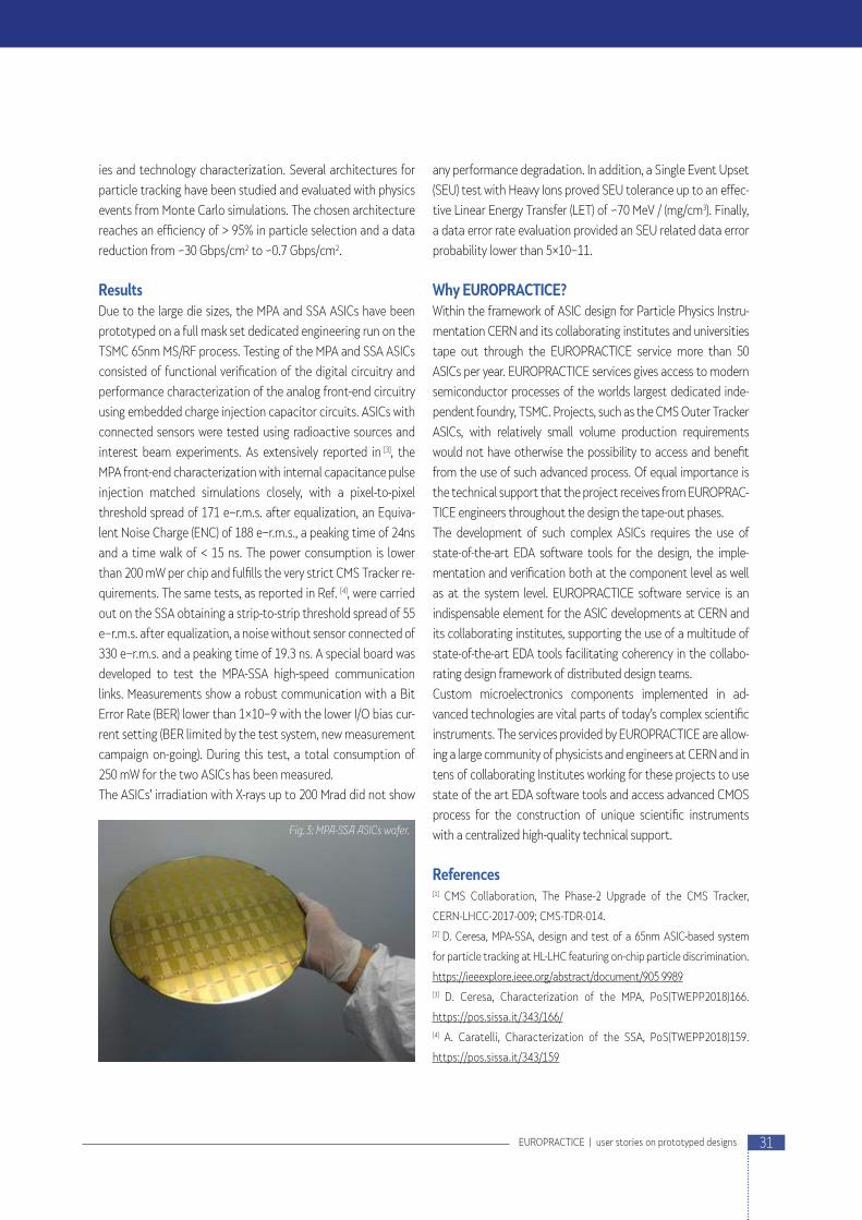
ies and technology characterization. Several architectures for
particle tracking have been studied and evaluated with physics
events from Monte Carlo simulations. The chosen architecture
reaches an efficiency of > 95% in particle selection and a data
reduction from ~30 Gbps/cm2 to ~0.7 Gbps/cm2.
ResultsDue to the large die sizes, the MPA and SSA ASICs have been
prototyped on a full mask set dedicated engineering run on the
TSMC 65nm MS/RF process. Testing of the MPA and SSA ASICs
consisted of functional verification of the digital circuitry and
performance characterization of the analog front-end circuitry
using embedded charge injection capacitor circuits. ASICs with
connected sensors were tested using radioactive sources and
interest beam experiments. As extensively reported in [3], the
MPA front-end characterization with internal capacitance pulse
injection matched simulations closely, with a pixel-to-pixel
threshold spread of 171 e−r.m.s. after equalization, an Equiva-
lent Noise Charge (ENC) of 188 e−r.m.s., a peaking time of 24 ns
and a time walk of < 15 ns. The power consumption is lower
than 200 mW per chip and fulfills the very strict CMS Tracker re-
quirements. The same tests, as reported in Ref. [4], were carried
out on the SSA obtaining a strip-to-strip threshold spread of 55
e−r.m.s. after equalization, a noise without sensor connected of
330 e−r.m.s. and a peaking time of 19.3 ns. A special board was
developed to test the MPA-SSA high-speed communication
links. Measurements show a robust communication with a Bit
Error Rate (BER) lower than 1×10⁻⁹ with the lower I/O bias cur-
rent setting (BER limited by the test system, new measurement
campaign on-going). During this test, a total consumption of
250 mW for the two ASICs has been measured.
The ASICs’ irradiation with X-rays up to 200 Mrad did not show
any performance degradation. In addition, a Single Event Upset
(SEU) test with Heavy Ions proved SEU tolerance up to an effec-
tive Linear Energy Transfer (LET) of ~70 MeV / (mg/cm3). Finally,
a data error rate evaluation provided an SEU related data error
probability lower than 5×10⁻¹¹.
Why EUROPRACTICE?Within the framework of ASIC design for Particle Physics Instru-
mentation CERN and its collaborating institutes and universities
tape out through the EUROPRACTICE service more than 50
ASICs per year. EUROPRACTICE services gives access to modern
semiconductor processes of the worlds largest dedicated inde-
pendent foundry, TSMC. Projects, such as the CMS Outer Tracker
ASICs, with relatively small volume production requirements
would not have otherwise the possibility to access and benefit
from the use of such advanced process. Of equal importance is
the technical support that the project receives from EUROPRAC-
TICE engineers throughout the design the tape-out phases.
The development of such complex ASICs requires the use of
state-of-the-art EDA software tools for the design, the imple-
mentation and verification both at the component level as well
as at the system level. EUROPRACTICE software service is an
indispensable element for the ASIC developments at CERN and
its collaborating institutes, supporting the use of a multitude of
state-of-the-art EDA tools facilitating coherency in the collabo-
rating design framework of distributed design teams.
Custom microelectronics components implemented in ad-
vanced technologies are vital parts of today’s complex scientific
instruments. The services provided by EUROPRACTICE are allow-
ing a large community of physicists and engineers at CERN and in
tens of collaborating Institutes working for these projects to use
state of the art EDA software tools and access advanced CMOS
process for the construction of unique scientific instruments
with a centralized high-quality technical support.
References[1] CMS Collaboration, The Phase-2 Upgrade of the CMS Tracker,
CERN-LHCC-2017-009; CMS-TDR-014. [2] D. Ceresa, MPA-SSA, design and test of a 65nm ASIC-based system
for particle tracking at HL-LHC featuring on-chip particle discrimination.
https://ieeexplore.ieee.org/abstract/document/905 9989 [3] D. Ceresa, Characterization of the MPA, PoS(TWEPP2018)166.
https://pos.sissa.it/343/166/ [4] A. Caratelli, Characterization of the SSA, PoS(TWEPP2018)159.
https://pos.sissa.it/343/159
Fig. 3: MPA-SSA ASICs wafer.
31EUROPRACTICE | user stories on prototyped designs

Mixed-Signal Neuromorphic Device HICANN-XElectronic Vision(s) Group, Kirchhoff Institute for Physics, Heidelberg University, Germany
Contact: Dr. Johannes Schemmel
E-mail: [email protected]
Technology: TSMC 65nm
Die size: 8mm × 4mm
Design tools: Cadence Virtuoso, Mentor ModelSim/Questa,
Cadence Xcelium, Synopsys Design Compiler, Cadence
Innovus, Synopsys Primetime, Mentor Calibre
DescriptionHeidelberg University has a more than 20-year history of
neuromorphic circuit design. The most recent generation
is the BrainScaleS-2 system. This tapeout comprised the
current revision of the BrainScaleS-2 system ASIC: a complex
mixed-signal system-on-a-chip supporting all aspects of
neuromorphic processing. It contains at its heart an analog
neural network core, consisting of 256k synapse circuits and
512 neuronal compartments. They operate 1000 times faster
than biological real-time, resulting in a maximum connection
rate of 32*1015 cps. The analog core simultaneously supports
spike or rate based neural modeling, making it suitable for
deep convolutional neural networks as well as event-based
processing after the biological example. The synapses include
temporal correlation sensors for online learning, which is
further supported by two on-die embedded Power-PC CPU
cores with 128-wide SIMD-processing extensions each. They
can access the analog correlation measurements as well as
the membrane voltages of all neuronal compartments with
two parallel ADC converters providing a total number of
1024 channels.
External communication is realized by eight source-synchro-
nous serial links with an aggregated bandwidth of 32 Gb/s.
The applications of the HICANN-X system are twofold: low-
power analog inference and modeling of biologically-inspired
online learning algorithms. For inference two operation
modes are available. Either a rate-based one, which allows
the direct implementation of DCNN models, or spike-based
coding, which is especially suited for extreme low-latency
inference. MNIST classification has been demonstrated with
an effective rate of 70k frames per second at 4 μJ per frame
while powering the full ASIC.
Fig.1: Layout view of HICANN-X.
Fig.2: Photograph of the fabricated chip.
As a modeling platform for biology, the BrainScaleS-2
architecture supports the Adaptive-Exponential-Integrate-
and-Fire neuron model with additional support for active
dendrites and structured neurons. Support circuits for
synaptic as well as structural plasticity are closely coupled to
the on-die SIMD cores, providing “hybrid plasticity”: plasticity
algorithms with most of the flexibility of software solutions
while still maintaining the speed and power-efficiency of a
fully parallel mixed-signal hardware implementation.
Why EUROPRACTICE?Heidelberg University has worked with EUROPRACTICE
on TSMC and other ICM fabrication on a multitude of
successful tapeouts since 1994. EUROPRACTICE has been
a reliable partner for all aspects of multi-project and full
maskset prototypes. The affordable access to multi-project
wafer and mini@sic fabrication has been an enabling factor
for our research in neuromorphic hardware.
AcknowledgementThe research has received funding from the
Bundesministeriums für Bildung und Forschung under the
funding no. 16ES1127 (HD-BIO-AI) and from the European
Union’s Horizon 2020 Framework Programme for Research
and Innovation under the Specific Grant Agreement Nos.
720270, 785907 and 945539 (Human Brain Project, HBP).
TSMC 65
32 EUROPRACTICE | user stories on prototyped designs
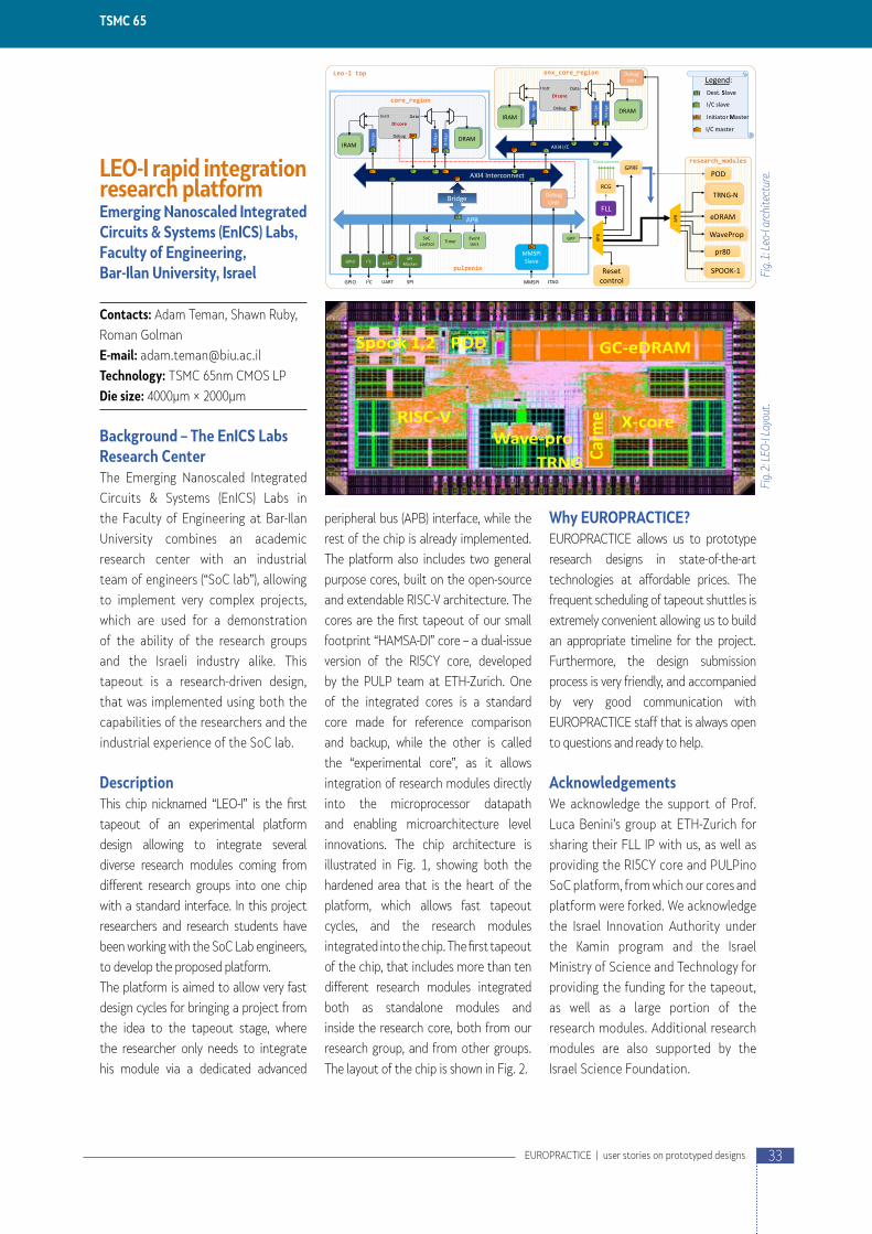
LEO-I rapid integration research platform Emerging Nanoscaled Integrated Circuits & Systems (EnICS) Labs, Faculty of Engineering, Bar-Ilan University, Israel
Contacts: Adam Teman, Shawn Ruby,
Roman Golman
E-mail: [email protected]
Technology: TSMC 65nm CMOS LP
Die size: 4000μm × 2000μm
Background – The EnICS Labs Research CenterThe Emerging Nanoscaled Integrated
Circuits & Systems (EnICS) Labs in
the Faculty of Engineering at Bar-Ilan
University combines an academic
research center with an industrial
team of engineers (“SoC lab”), allowing
to implement very complex projects,
which are used for a demonstration
of the ability of the research groups
and the Israeli industry alike. This
tapeout is a research-driven design,
that was implemented using both the
capabilities of the researchers and the
industrial experience of the SoC lab.
DescriptionThis chip nicknamed “LEO-I” is the first
tapeout of an experimental platform
design allowing to integrate several
diverse research modules coming from
different research groups into one chip
with a standard interface. In this project
researchers and research students have
been working with the SoC Lab engineers,
to develop the proposed platform.
The platform is aimed to allow very fast
design cycles for bringing a project from
the idea to the tapeout stage, where
the researcher only needs to integrate
his module via a dedicated advanced
peripheral bus (APB) interface, while the
rest of the chip is already implemented.
The platform also includes two general
purpose cores, built on the open-source
and extendable RISC-V architecture. The
cores are the first tapeout of our small
footprint “HAMSA-DI” core – a dual-issue
version of the RI5CY core, developed
by the PULP team at ETH-Zurich. One
of the integrated cores is a standard
core made for reference comparison
and backup, while the other is called
the “experimental core”, as it allows
integration of research modules directly
into the microprocessor datapath
and enabling microarchitecture level
innovations. The chip architecture is
illustrated in Fig. 1, showing both the
hardened area that is the heart of the
platform, which allows fast tapeout
cycles, and the research modules
integrated into the chip. The first tapeout
of the chip, that includes more than ten
different research modules integrated
both as standalone modules and
inside the research core, both from our
research group, and from other groups.
The layout of the chip is shown in Fig. 2.
Why EUROPRACTICE?EUROPRACTICE allows us to prototype
research designs in state-of-the-art
technologies at affordable prices. The
frequent scheduling of tapeout shuttles is
extremely convenient allowing us to build
an appropriate timeline for the project.
Furthermore, the design submission
process is very friendly, and accompanied
by very good communication with
EUROPRACTICE staff that is always open
to questions and ready to help.
AcknowledgementsWe acknowledge the support of Prof.
Luca Benini’s group at ETH-Zurich for
sharing their FLL IP with us, as well as
providing the RI5CY core and PULPino
SoC platform, from which our cores and
platform were forked. We acknowledge
the Israel Innovation Authority under
the Kamin program and the Israel
Ministry of Science and Technology for
providing the funding for the tapeout,
as well as a large portion of the
research modules. Additional research
modules are also supported by the
Israel Science Foundation.
TSMC 65
Leo-I SoC
FLL
AXI4 I/C
Leo-I top
mm m
s
s s
S
Legend:
s
Dest. Slave
I/C slave
M
m
Initiator Master
I/C master
AXI4 Interconnect
APB
Bridge
SoC control Timer Event
Unit
MMSPI Slave
Debug Unit
GPIO
GPIO
UART
UART
I2C
I2C
SPI Master
SPI MMSPI JTAG
pulpenix
S
m m
m
s
s
IRAM Brid
ge DRAM
Instr
Brid
ge
Brid
ge
DI core
core_region
Debug
Data
SMS
GPP
M
s
M
s s m
IRAM Brid
ge DRAM
Instr
Brid
ge
Brid
ge
DI core
enx_core_region
Debug
Data
SMS
M
APB
RCG
GPRF
Reset control
Clock sources
M
Debug Unit
APB
POD
TRNG
eDRAM
pr80
SPOOK-0
WaveProp
research_modules
SPOOK-1
TRNGTRNG-N
GC-eDRAM
X-coreRISC-VWave-pro
Spook 1,2 POD
Carm
e
TRNG
Fig.
1: Le
o-I a
rchi
tect
ure.
Fig.
2: L
EO-I
Layo
ut.
33EUROPRACTICE | user stories on prototyped designs

Rosetta: PULP-based in-memory computing research vehicleETH Zürich, EPFL, Switzerland
Contacts: Manuel Eggimann, Alexandre Levisse, Robert Giterman
E-mail: [email protected]
Technology: TSMC 65nm CMOS
Die size: 2940μm × 4080μm
Design tools: Synopsys: Design Compiler; Cadence Design
Systems: Innovus; Mentor: Questasim, Calibre
DescriptionRosetta is a research SoC designed around the PULPissimo
architecture part of the open-source PULP platform (https://
pulp-platform.org/ ). The basis is a RISC-V based microcontroller
system running at 200MHz including 512kBytes of on-chip
SRAM and a wide set of common peripherals such as QSPI, I2C,
I2S, Camera Interface, UART and a JTAG-based RISC-V debug
specification compliant debug unit with full access to the main
memory bus of the system.
The most interesting aspect of the PULPissimo system is
that it allows the addition of hardware accelerators that have
direct access to the processor memory with relative ease. In
Rosetta, the independent work of three different research
groups was combined in one SoC. By sharing a common
processing infrastructure and memory, the research groups
were able to focus their work on their research and develop
their own accelerators. The flexibility of the PULPissimo
allowed these independent systems to be manufactured
within the same SoC without interfering with each other
while allowing greater flexibility for testing and evaluation.
The contribution of the Integrated Circuits Laboratory of ETH
Zurich is a programmable autonomous accelerator for Hyper-
Dimensional Computing Algorithms with binary-spatter-code
based hypervectors of dimensionality of up to 2048 bits.
The Embedded Systems Laboratory of EPFL, Lausanne has
contributed a 32KiB in-sram computing architecture and
an innovative memory controller enabling in-situ bitwise
operations, addition and multiplications. These features will
be used to accelerate data-intensive applications running on
the PULPissimo platform.
Finally, the Telecommunication Circuits Laboratory of EPFL
developed a 64 KiB (in 16 memory cuts) of Gain-Cell eDRAM,
based on conventional logic design rules, which can offer
higher density than SRAM. The eDRAM in this implementation
has a built-in refresh support and a new option to ease folding
of the memory. By adjusting the refresh period, it will be used
to explore approximate-computing concepts.
While these systems are designed to operate independently,
the PULPissimo system also allows these systems to work
concurrently, for example the hyper-dimensional computing
accelerator is able to use both its own standard cell based
memories operating at low voltages or the eDRAM operating
with long refresh periods to explore energy reliability trade-
offs in such configurations.
The chip is named after the Rosetta Stone that contains
the same script in three alphabets and was instrumental in
deciphering hieroglyphs. This chip contains the work of three
different research groups and the high dimensional computing
accelerator has applications in language recognition.
Why EUROPRACTICE?Over the years, the Integrated Systems Laboratory of ETH
Zurich has been able to design and get more than 200 ASICs
manufactured through the active and invaluable support of both
the EUROPRACTICE Design Tool Service which allows us to have
access to state of the art IC Design software not only for research
but also for in-class use and of course the EUROPRACTICE IC
manufacturing service that has been instrumental in our ability
to be engaged in IC Design at this level.
EUROPRACTICE is not only a service for us, but a partner that
helps us with the correct choice of technology, packaging as
well as supporting us in all aspects of the design process.
Acknowledgements Part of the work was supported by the European Union’s
Horizon 2020 Research and Innovation Programme under
grant agreement No 780215, Mnemosene.
TSMC 65
Fig.1: Rosetta dies in a waffle pack.
34 EUROPRACTICE | user stories on prototyped designs

CMOS reservoir computer for intelligent wearable health monitors Electrical Engineering, University at Buffalo, State University of New York, NY, USA
Contacts: Arindam Sanyal, Sanjeev Tannirkulam Chandrasekaran
E-mail: [email protected]
Technology: TSMC 65nm 1p9M
Die size: 1.2mm × 0.7mm
DescriptionEarly detection of stress and heart diseases can prevent one-
third of global deaths. Advances in machine learning (ML) has
the potential for automating risk prediction of heart diseases
by analyzing patient vitals in combination with electronic
healthcare record (EHR). Embedding ML algorithms on
wearable devices can lead to continuous intelligent health
monitoring of patients. However, conventional ML algorithms
are computationally intensive and consume significant energy
during a memory access, which makes their integration on
resource-constrained wearables challenging. Prior attempts
have addressed this issue through reduced bit-precision, in-
memory computation, and reduced number of multipliers.
However, they consume energy in the range of hundreds of nJ
to tens of μJ for each inference.
Instead of optimizing existing ML architectures, we
demonstrate the first reservoir-computing based RCML
architecture that consumes factors-of-magnitude lower
energy than conventional ML algorithms without sacrificing
accuracy. The RC mimics a non-linear kernel and projects
the input to a higher-dimensional space, thereby enabling
classification of the data with simple logistic regression (LR)
output layer. We demonstrate the RC chip for detecting stress
and heart diseases from electrocardiogram (ECG) signal and
electronic healthcare record (EHR). Operating from a 1.2V
supply, the RC can detect stress from ECG signals in real-time
with 93% accuracy, while consuming 27.5nJ/inference, which
is 7x better than existing state-of-the-art ECG processors. The
RC is capable of early prediction of heart diseases with 84%
accuracy while consuming 7.5nJ/inference, which is 44x better
than existing state-of-the-art neural networks ICs employed
for medical event classification.
Why EUROPRACTICE? EUROPRACTICE offers affordable prototyping for research and
it is much simpler to use their PDK and services compared to
competitors in the USA. The EUROPRACTICE and imec staff
are also easily accessible and have always answered all our
questions patiently and helped us with all our prototypes.
AcknowledgementThis material is based on research sponsored by US Air
Force Research Laboratory under agreement number
FA8650-18-2-5402.
TSMC 65
C-D
ACSAR
R-DAC
Del
ay L
ine
OTA+non-linearity
Output buffer
0.04 0.06-0.2
-0.1
0
0.1
0.2Before RC
-0.05 0 0.05 0.1-0.2
-0.1
0
0.1
0.2
no stressstress
no stressstress normal stress
Predicted Class
normal
stress
Tru
e Cla
ss
29
18142
108
After RC
Fig.1: RCNN chip for stress detection from ECG.
35EUROPRACTICE | user stories on prototyped designs

ALTIROC1, a 25 ps jitter ASIC for the ATLAS High Granularity Timing Detector (HGTD) OMEGA (CNRS/IN2P3), Ecole Polytechnique, Palaiseau, FranceSLAC National Accelerator Laboratory, Stanford University, Menlo Park, California
Contacts: Nathalie Seguin-Moreau, Bojan Markovic
E-mails: [email protected], [email protected]
Technology: TSMC 0.13μm CMOS MS/RF (8-inch)
Die size: 7600μm × 7700μm
Description ALTIROC1 is a 25-channel ASIC prototype designed in TSMC
130 nm to read out a 5 × 5 channel matrix of 1.3mm × 1.3mm
Low Gain Avalanche Diodes (LGAD) of the new ATLAS HGTD
detector foreseen for the High Luminosity-LHC upgrade, where
high radiation levels are expected (200 Mrad and 2.5 1015 MeV
neq/cm2 fluence). The dies will be bump-bonded onto sensors.
The targeted combined time resolution of the system sensor
+ readout electronics is 25 ps for 10 fC input charges.
The ASIC noise must be small enough to detect charges as
small as 4 fC with a 95 % efficiency.
This ASIC comprises several analog and digital blocks. Each
channel integrates a RF preamplifier (1 GHz bandwidth)
followed by a large gain leading edge discriminator and two
Time to Digital Converters (TDC) for Time-of-Arrival (TOA)
and Time-Over-Threshold (TOT) measurements. The timing
data are stored in a local memory. The TOA and TOT TDCs
achieve a 20 ps time resolution over a 2.5 ns range and 40 ps
over a 20 ns range respectively. Measurements gave a DNL
of about 6 ps rms and time resolution dispersion between
channels of 0.35 rms after individual tunings. This frontend
exhibits a 20 ps jitter noise for a detector capacitance of 5
pF and an input charge of 5 fC while keeping a challenging
power consumption of less than 4.5 mW per channel.
Furthermore, the ASIC has out-of-pixel analog and digital
blocks. In particular, it includes a 1.28 GHz PLL providing
multiples of 40 MHz clocks and a phase shifter with 100 ps
phase shift resolution over a 25 ns range.
Why EUROPRACTICE? The EUROPRACTICE service offers the ability to reduce
manufacturing costs thanks to large multi-project wafers.
TSMC 130
Fig.1: ASIC layout
Fig.2: ASIC bump bonded onto a sensor
GAMMA2 Fig.3: Measured EEG-signal, showing blinking eyes.
36 EUROPRACTICE | user stories on prototyped designs
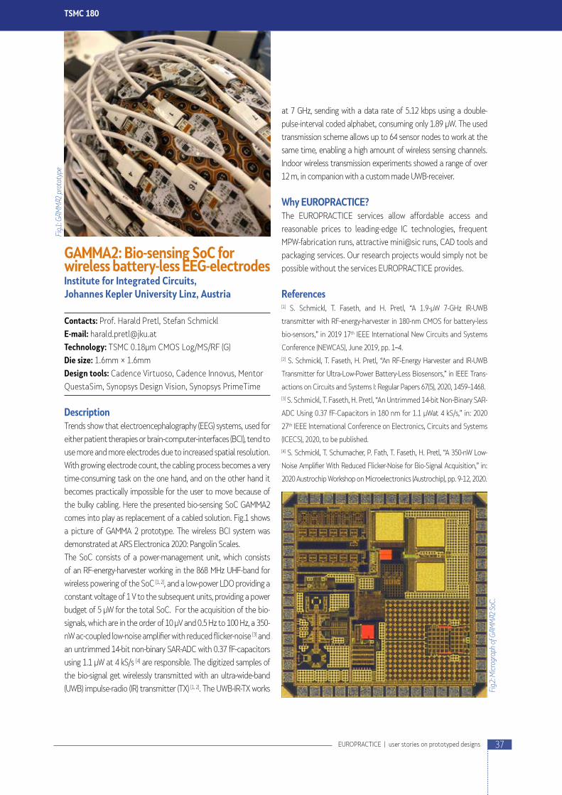
GAMMA2: Bio-sensing SoC for wireless battery-less EEG-electrodesInstitute for Integrated Circuits, Johannes Kepler University Linz, Austria
Contacts: Prof. Harald Pretl, Stefan Schmickl
E-mail: [email protected]
Technology: TSMC 0.18μm CMOS Log/MS/RF (G)
Die size: 1.6mm × 1.6mm
Design tools: Cadence Virtuoso, Cadence Innovus, Mentor
QuestaSim, Synopsys Design Vision, Synopsys PrimeTime
DescriptionTrends show that electroencephalography (EEG) systems, used for
either patient therapies or brain-computer-interfaces (BCI), tend to
use more and more electrodes due to increased spatial resolution.
With growing electrode count, the cabling process becomes a very
time-consuming task on the one hand, and on the other hand it
becomes practically impossible for the user to move because of
the bulky cabling. Here the presented bio-sensing SoC GAMMA2
comes into play as replacement of a cabled solution. Fig.1 shows
a picture of GAMMA 2 prototype. The wireless BCI system was
demonstrated at ARS Electronica 2020: Pangolin Scales.
The SoC consists of a power-management unit, which consists
of an RF-energy-harvester working in the 868 MHz UHF-band for
wireless powering of the SoC [1, 2], and a low-power LDO providing a
constant voltage of 1 V to the subsequent units, providing a power
budget of 5 μW for the total SoC. For the acquisition of the bio-
signals, which are in the order of 10 μV and 0.5 Hz to 100 Hz, a 350-
nW ac-coupled low-noise amplifier with reduced flicker-noise [3] and
an untrimmed 14-bit non-binary SAR-ADC with 0.37 fF-capacitors
using 1.1 μW at 4 kS/s [4] are responsible. The digitized samples of
the bio-signal get wirelessly transmitted with an ultra-wide-band
(UWB) impulse-radio (IR) transmitter (TX) [1, 2]. The UWB-IR-TX works
at 7 GHz, sending with a data rate of 5.12 kbps using a double-
pulse-interval coded alphabet, consuming only 1.89 μW. The used
transmission scheme allows up to 64 sensor nodes to work at the
same time, enabling a high amount of wireless sensing channels.
Indoor wireless transmission experiments showed a range of over
12 m, in companion with a custom made UWB-receiver.
Why EUROPRACTICE?The EUROPRACTICE services allow affordable access and
reasonable prices to leading-edge IC technologies, frequent
MPW-fabrication runs, attractive mini@sic runs, CAD tools and
packaging services. Our research projects would simply not be
possible without the services EUROPRACTICE provides.
References[1] S. Schmickl, T. Faseth, and H. Pretl, “A 1.9-μW 7-GHz IR-UWB
transmitter with RF-energy-harvester in 180-nm CMOS for battery-less
bio-sensors,” in 2019 17th IEEE International New Circuits and Systems
Conference (NEWCAS), June 2019, pp. 1–4.[2] S. Schmickl, T. Faseth, H. Pretl, “An RF-Energy Harvester and IR-UWB
Transmitter for Ultra-Low-Power Battery-Less Biosensors,” in IEEE Trans-
actions on Circuits and Systems I: Regular Papers 67(5), 2020, 1459–1468.[3] S. Schmickl, T. Faseth, H. Pretl, “An Untrimmed 14-bit Non-Binary SAR-
ADC Using 0.37 fF-Capacitors in 180 nm for 1.1 μWat 4 kS/s,” in: 2020
27th IEEE International Conference on Electronics, Circuits and Systems
(ICECS), 2020, to be published.[4] S. Schmickl, T. Schumacher, P. Fath, T. Faseth, H. Pretl, “A 350-nW Low-
Noise Amplifier With Reduced Flicker-Noise for Bio-Signal Acquisition,” in:
2020 Austrochip Workshop on Microelectronics (Austrochip), pp. 9-12, 2020.
TSMC 180
Fig.2
: Mic
rogr
aph
of G
AMM
A2 S
oC.
Fig.1
: GAM
MA2
pro
toty
pe
37EUROPRACTICE | user stories on prototyped designs
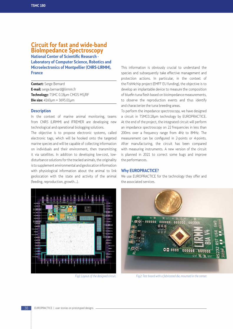
Circuit for fast and wide-band BioImpedance Spectroscopy National Center of Scientific Research - Laboratory of Computer Science, Robotics and Microelectronics of Montpellier (CNRS-LIRMM), France
Contact: Serge Bernard
E-mail: [email protected]
Technology: TSMC 0.18μm CMOS MS/RF
Die size: 4160μm × 3695.01μm
DescriptionIn the context of marine animal monitoring, teams
from CNRS (LIRMM) and IFREMER are developing new
technological and operational biologging solutions.
The objective is to propose electronic systems, called
electronic tags, which will be hooked onto the targeted
marine species and will be capable of collecting information
on individuals and their environment, then transmitting
it via satellites. In addition to developing low-cost, low-
disturbance solutions for the tracked animals, the originality
is to supplement environmental and geolocation information
with physiological information about the animal to link
geolocation with the state and activity of the animal
(feeding, reproduction, growth…).
This information is obviously crucial to understand the
species and subsequently take effective management and
protection actions. In particular, in the context of
the FishNchip project (EMFF EU funding), the objective is to
develop an implantable device to measure the composition
of bluefin tuna flesh based on bioimpedance measurements,
to observe the reproduction events and thus identify
and characterize the tuna breeding areas.
To perform the impedance spectroscopy, we have designed
a circuit in TSMC0.18μm technology by EUROPRACTICE.
At the end of the project, the integrated circuit will perform
an impedance spectroscopy on 22 frequencies in less than
200ms over a frequency range from 4Hz to 8MHz. The
measurement can be configured in 2-points or 4-points.
After manufacturing, the circuit has been compared
with measuring instruments. A new version of the circuit
is planned in 2021 to correct some bugs and improve
the performances.
Why EUROPRACTICE?We use EUROPRACTICE for the technology they offer and
the associated services.
TSMC 180
Fig1: Layout of the designed circuit. Fig.2: Test board with a fabricated die, mounted in the center.
38 EUROPRACTICE | user stories on prototyped designs
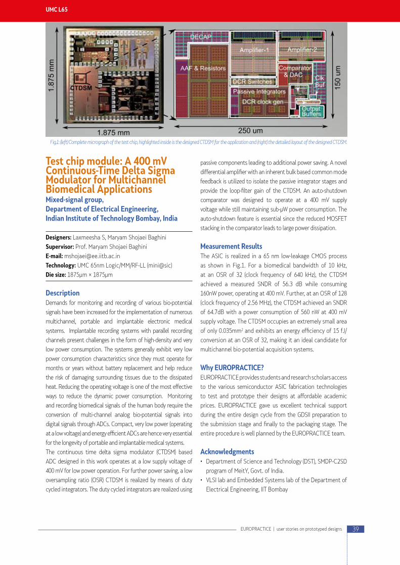
Test chip module: A 400 mV Continuous-Time Delta Sigma Modulator for Multichannel Biomedical ApplicationsMixed-signal group, Department of Electrical Engineering, Indian Institute of Technology Bombay, India
Designers: Laxmeesha S, Maryam Shojaei Baghini
Supervisor: Prof. Maryam Shojaei Baghini
E-mail: [email protected]
Technology: UMC 65nm Logic/MM/RF-LL (mini@sic)
Die size: 1875μm × 1875μm
DescriptionDemands for monitoring and recording of various bio-potential
signals have been increased for the implementation of numerous
multichannel, portable and implantable electronic medical
systems. Implantable recording systems with parallel recording
channels present challenges in the form of high-density and very
low power consumption. The systems generally exhibit very low
power consumption characteristics since they must operate for
months or years without battery replacement and help reduce
the risk of damaging surrounding tissues due to the dissipated
heat. Reducing the operating voltage is one of the most effective
ways to reduce the dynamic power consumption. Monitoring
and recording biomedical signals of the human body require the
conversion of multi-channel analog bio-potential signals into
digital signals through ADCs. Compact, very low power (operating
at a low voltage) and energy efficient ADCs are hence very essential
for the longevity of portable and implantable medical systems.
The continuous time delta sigma modulator (CTDSM) based
ADC designed in this work operates at a low supply voltage of
400 mV for low power operation. For further power saving, a low
oversampling ratio (OSR) CTDSM is realized by means of duty
cycled integrators. The duty cycled integrators are realized using
passive components leading to additional power saving. A novel
differential amplifier with an inherent bulk based common mode
feedback is utilized to isolate the passive integrator stages and
provide the loop-filter gain of the CTDSM. An auto-shutdown
comparator was designed to operate at a 400 mV supply
voltage while still maintaining sub-μW power consumption. The
auto-shutdown feature is essential since the reduced MOSFET
stacking in the comparator leads to large power dissipation.
Measurement ResultsThe ASIC is realized in a 65 nm low-leakage CMOS process
as shown in Fig.1. For a biomedical bandwidth of 10 kHz,
at an OSR of 32 (clock frequency of 640 kHz), the CTDSM
achieved a measured SNDR of 56.3 dB while consuming
160 nW power, operating at 400 mV. Further, at an OSR of 128
(clock frequency of 2.56 MHz), the CTDSM achieved an SNDR
of 64.7 dB with a power consumption of 560 nW at 400 mV
supply voltage. The CTDSM occupies an extremely small area
of only 0.035 mm2 and exhibits an energy efficiency of 15 fJ/
conversion at an OSR of 32, making it an ideal candidate for
multichannel bio-potential acquisition systems.
Why EUROPRACTICE?EUROPRACTICE provides students and research scholars access
to the various semiconductor ASIC fabrication technologies
to test and prototype their designs at affordable academic
prices. EUROPRACTICE gave us excellent technical support
during the entire design cycle from the GDSII preparation to
the submission stage and finally to the packaging stage. The
entire procedure is well planned by the EUROPRACTICE team.
Acknowledgments• Department of Science and Technology (DST), SMDP-C2SD
program of MeitY, Govt. of India.
• VLSI lab and Embedded Systems lab of the Department of
Electrical Engineering, IIT Bombay
UMC L65
Fig.1: (left) Complete micrograph of the test chip, highlighted inside is the designed CTDSM for the application and (right) the detailed layout of the designed CTDSM.
39EUROPRACTICE | user stories on prototyped designs

Programmable Readout IC for Photodiodes ArrayŁukasiewicz Research Network - Institute of Mi-croelectronics and Photonics, Warsaw, Poland
Contacts: Cezary Kolacinski*, Pawel Pienczuk, Andrzej
Szymanski and Dariusz Obrebski
E-mail: [email protected]
Technology: UMC L180 MM/RF
Die size: 4960μm × 1525μm
Design tool: Cadence Design Systems
DescriptionUnder the ParCour project, the established consortium
develops a new particle counting technique, with an aim
of cost and mobility. A new measurement apparatus will be
based on a LED light source, additional optical systems, a
unique photodiodes (PDs) array and a designed integrated
circuit for readout. The PDs array is organized as a half
ring structure consisting of 17 sections with different sizes
and position - this structure has been manufactured
using proprietary CMOS process of the Institute of
Microelectronics and Photonics.
Dedicated readout chip – designed in UMC L180 MM/RF
process - features 17 analog input ports, 17 analog output
ports, SPI bus and several diagnostic and auxiliary ports.
Designed analog block consists of 17 separate channels,
one for each photodiode forming the detection array. Signal
path of each channel is composed of two amplification
blocks: a transimpedance amplifier (TIA) and a voltage
amplifier (buffer). Parameters of the particular channel has
been suited to the expected characteristic of corresponding
PD but the values of offset and current-to-voltage ratio
(transconductance) can be controlled (within the limited
range) by the 4-bit digital signals, independently for each
channel.
Digital interface configures the analog block parameters – it
consists of several calibration registers, accessible via the
Serial Peripheral Interface (SPI). Power-on Reset (PoR) block
resets registers at every power-up event.
Every time the power supply is switched on, the configuration
process must be performed. It is realized with the mentioned
SPI protocol and 2-byte data frame. Each configuration word
addresses particular register in specific channel and passes
4-bit value in 11 least-significant bits. Last 5 bits are ignored.
The channel to be controlled is addressed by 5 LSBs within
the frame, while the register – by subsequent two bits.
Total current consumption has been estimated at 10mA
for the complete chip (at 3.3V power supply). The structure
fabricated in UMC CMOS 180nm technology occupies area
of 4960μm x 1525μm and is equipped with 57 I/O pads.
Why EUROPRACTICE?Łukasiewicz Research Network - Institute of Microelectronics
and Photonics (formerly Institute of Electron Technology) is
a longstanding member of EUROPRACTICE, with many ICs
designed and fabricated over the last twenty years. The
EUROPRACTICE MPW service offers an excellent opportunity
for the prospective access to many mature technologies.
EUROPRACTICE staff always provides superb assistance and
knowledgeable feedback, which is a huge support for our
design and prototyping processes.
AcknowledgementThis work has been supported by Poland Berlin-Brandenburg
Project no. 2/POLBER-3/2018 Parcour — “Particle counter”.
UMC L180
Fig.1: Layout of the designed structure (left) and fabricated chip mounted in PLCC package (right).
40 EUROPRACTICE | user stories on prototyped designs

ReSCU-V2: SIL3 Safe-SoC according to IEC 61508Institute for Computer Architecture and System Programming (ICAS), University of Kassel, Germany
Contacts: Prof. Dr.-Ing. Josef Börcsök, M. Sc. Waldemar Müller,
M. Sc. Eike Hahn
E-mail: [email protected]
Technology: UMC L180 MM/RF 1.8V/3.3V 1P6M
Die size: 5mm × 5mm
Design tools: Cadence digital design flow
IntroductionToday, in addition to system size, reduced system costs,
optimized energy consumption and high reliability or safety,
the aspects of functional safety are increasingly in the focus
of many applications.
DescriptionThe ReSCU-V2 safety chip consists of a 1oo2D safety
architecture model (Fig.1) based on an asynchronous
software comparator architecture. The design of the safety
SoC is realized according to IEC 61508 standard. Internally
the architecture has two redundant 32-bit microcontrollers of
type ColdFireV2. Each side consists of 16KiB Cache and 32KiB
SRAM, both enhanced with SECDED, as well as ethernet, QSPI,
I2C, UART and CAN as peripherals. The complete SoC also
features 78 FlexIO and 20 PWM, multiplexed with peripheral
functions, as well as 8 ADC and 4 DAC channels. All FlexIO are
equipped with real-time hardware on-chip diagnosis for every
single IO, including self-test, that detects multiplexer status
and correct function of the IO up to the bond pad without
software intervention. ADC and DAC are also redundant, as
well as isolated and provide diagnosis features. On top, there
is a physically isolated watchdog on chip.
Both microprocessor systems are independent from
clock, power and memory, called by standard free from
interference. For crosschecking the safety-relevant results of
both processors, they can communicate on-chip by two fast
asynchronous interfaces.
Freedom from interference is also concerned for the back-
end design, so both microprocessor systems are physically
isolated by a 100µm wide gap. Additionally, all supply voltages
need to be independent, which leads to eight power domains
on chip for I/O, core, PLL and analog parts on both channels.
The SoC was packaged into a CPGA256 package. It consumes
< 500mW and runs stable at 100MHz from -40°C to +125°C.
Why EUROPRACTICE?EUROPRACTICE gives the possibility to realize small research
projects with limited funding. Additionally, the support by
EUROPRACTICE for software and design issues is of big
importance for small research groups.
Referenceshttp://www.uni-kassel.de/eecs/fachgebiete/icas/forschung/system-on-a-chip-soc/rescu-v2.html
UMC L180
Fig.1: 1oo2D safety concept.
Fig.2: Physical layout of the safety SoC.
Fig.3: Photo of the ReSCU-V2 die.
41EUROPRACTICE | user stories on prototyped designs

NIRCA MkII - Control ASIC for IR image sensorsIntegrated Detector Electronics AS (IDEAS), Oslo, Norway
Contacts: Amir Hasanbegovic, Gunnar Maehlum
E-mail: [email protected]
Technology: UMC L180 Logic GII, Mixed-Mode/RF
Die size: 10mm × 10mm
DescriptionNIRCA MkII is the second-generation ASIC from IDEAS for
readout from infrared (IR) image sensors, e.g., HgCdTe/MCT-
based focal plane arrays (FPA). The ASIC aims at reducing
the size, weight, power and cost (SWaP-C) of infrared sensor
readout systems by integrating the necessary functions and
performance on a single ASIC. The NIRCA MkII is a radiation-
tolerant integrated circuit (IC) system-on-chip with operating
temperature between -40°C and +85°C. This makes the
ASIC highly suitable for meeting the requirements in Earth
observation payloads on satellites. The illustration shows the
die photo of the ASIC (with annotations). The ASIC includes
16 video channels (VADCs) and 1 auxiliary ADC (AADC), each
with a 1x to 8x programmable gain amplifier and a pipeline
ADC with 14-bit and 16-bit output options running at 12
Msps. Analog input offset is adjustable in the analog domain
(SREF) with fine-tuning of gain and offset is possible in the
digital domain. Digitized sensor data is output on a 9x480-
Mbps high-speed serial LVDS interface. The ASIC provides a
digital interface (DIN/DOUT) for controlling the sensor, and
analog reference voltages (ODAC) for biasing the sensor.
NIRCA MkII is programmed via an SPI interface. After a
program has been loaded into the internal ECC RAM the
internal sequencer can execute a variety of tasks, e.g.,
waveform generation, ADC sampling control, configuration
and control of both internal analog and digital modules. The
validation campaign is currently ongoing, and the results so
far have been satisfactory.
Why EUROPRACTICE?To make this design, we worked closely with imec, who
provided IP and chip verification services. The design was
submitted for fabrication by using EUROPRACTICE MPW
services.
AcknowledgementsThe NIRCA MkII ASIC is developed under the ESA project
Control ASIC for Earth Observation Infrared Detector (ESA
Contract No. 4000119554/17/NL/BJ). The project has been
funded by the European Space Agency (ESA), the Norwegian
Space Agency (NSA) and IDEAS.
UMC L180
Fig.1: Bare die of NIRCA MkII.
42 EUROPRACTICE | user stories on prototyped designs

Read-out ASIC for GEM detectorsASIC Lab, National Research Nuclear University «MEPhI», Moscow, Russia
Contacts: Eduard V. Atkin, Vitaly Shumikhin
E-mail: [email protected]
Technology: UMC L180 Mixed-Mode/RF
Die size: 3240μm × 1525μm
DescriptionNowadays gas electron multiplier (GEM) detectors are widely
used in large-scale physical experiments, such as MPD
(NICA), CBM (FAIR). During last few years a multichannel
readout ASIC for GEM detectors with an asynchronous (self-
triggered) architecture has been developed.
The developed ASIC is intended for read-out signals
coming from GEM detectors. The prototype version of the
ASIC contains 8 analog front-end channels for processing
signals of both polarities up to 100 fC at maximum
detector capacitance of 100 pF, followed by a 10-bit ADC
in each channel and a digital signal processing system. After
amplification and filtering of the detector signal in the
analog channel, the ADC converts it at a maximum sampling
rate of 25 MHz.
The chip has two modes of operation. In test mode, digital
data from the ADC is serialized and directly buffered by mean
of differential SLVS transmitters, working at a maximum
frequency of 320 MHz. In operating mode, the data from
the ADC of each channel is additionally processed by the
interpolator. A slow serial interface is used to control the
operation modes of the ASIC. To generate the clock signals
in the chip the phase-locked loop unit (PLL) is used.
A specific feature of the chip is a usage of the digital domain
interpolator for amplitude measurements. Using of the
interpolator allows determining signal maximum in ASIC at
high accuracy: 1 LSB for 10 bits ADC (simulation results).
ResultsThe ASIC has been implemented in 0.18 μm UMC L180 Mixed-Mode/
RF CMOS process and packaged into CPGA 120 case. The layout and
die photo are shown in Fig. 1. The lab measurement setup, shown in
Fig. 2, has confirmed the expected ASIC functionality.
Why EUROPRACTICE?EUROPRACTICE provides a unique opportunity for our University
to have a well-scheduled access to a wide range of advanced
technological processes. It is also important, that the approach
is cost-effective. This allows making a simple choice of right
technology for each R&D project, keeping in mind possibility of
further engineering runs for a small volume reproduction of chips.
An expert support on installation and usage of PDKs jointly with
advanced EDA tools gives additional benefit to our designers.
AcknowledgementThis work was supported by Grant No. 18-79-10259 of the
Russian Science Foundation.
UMC L180
Fig.1: ASIC layout versus die photo.
Fig.2: Lab measurement setup.
43EUROPRACTICE | user stories on prototyped designs

Servo Drive Controller ASICFaculty of Engineering, Technical University of Applied Sciences Rosenheim, Germany
Contact: Dr. Martin Versen
E-mail: [email protected]
Technology: X-FAB XH018 0.18μm E-FLASH MET3/4/MID/THK
Die size: 3226μm × 2962μm
Design tools: Cadence: Virtuoso, Genus, Innovus
Description Position-controlled servo drives are widely used in automation
systems. A cascaded control structure with a current
controller as innermost control loop is used. As controller
usually consists of proportional, integral and differential
(PID) elements, the motor control ASIC is a configurable PID
controller. The configuration is achieved by a serial peripheral
interface (SPI). The motor controller acts a SPI slave. Digital
inputs connect to three delta-sigma modulators which
sample at an input frequency of 16MHz. One analog input
receives a current input signal, while the other two interface
to the A/B signal of a rotary or a linear encoder. Three sinc3
decimation filters are implemented with variable filter lengths
between 16 and 256 to reduce the noise of the serial 1-bit
input data streams. For the motor control, the output signal
switches a full bridge assembly with an adjustable resolution
of up to 16bit with a device frequency of 100MHz. The project
includes a digital output interface for two 16bit digital-
analog converters (DAC) so that we can visualize control loop
variables with an oscilloscope on-line.
The servo drive controller is going to be used in lab practices
for mixed-signal systems in the master program of the
university.
Why EUROPRACTICE? The Technical University of Applied Sciences Rosenheim has
licensed Cadence Tools through EUROPRACTICE for several
years. We have benefitted from EUROPRACTICE’s excellent
technical support for dummy fill, chip submission and chip
packaging. EUROPRACTICE has given us an affordable access
to a multi-project wafer fabrication run.
X-FAB XH018
Fig.2: Microscope views of the fabricated chip
Fig.1: Layout view of the servo drive controller
44 EUROPRACTICE | user stories on prototyped designs

Calibration pulser for high energy physics ATLAS detector at CERNCentre de Microélectronique OMEGA – CNRS/IN2P3-Ecole Polytechnique, Palaiseau, France
Contact: Gisele Martin-Chassard
E-mail: [email protected]
Technology: XFAB XT018 0.18μm
Die size: 4.2mm × 2mm
Design tool: Mentor Calibre
IntroductionThe ASIC calib_atlas will provide the calibration of the
electromagnetic calorimeter for ATLAS experiment at CERN.
The goal of the circuit is to generate variable high precision
test pulses in each measurement channel of the detector over
the whole energy range (16bits).
DescriptionThe chip embeds a 16bit-DAC current followed by four high-
frequency switches to provide four calibration channels as
shown in the figure of the chip layout.
The 16bits DAC provides a current from 5μA (LSB) to 320mA
with an integral non-linearity less than 0.1% in the 10-bits DAC
range. Thanks to XFAB 10V transistors, we could make the
high-frequency switches so that the output pulse could reach
7.5V on 25 Ohms load. The 6 metal levels are very efficient to
drive properly a relatively high current.
ResultsThe dies are packed in QFN64 case. The tests show good
results in term of dynamic range and linearity for the switch
part, but more mitigated results for the 13-bit and 16-
bit DAC parts. The chip, which will be used in high energy
physics experiment, must be characterized in irradiation
environment. Irradiation tests were performed in X-ray beam
up to 3Mrad at CERN and in proton beam until 4 Mrad using
Proton Irradiation Facility (PIF) of Paul Scherrer Institut (PSI).
These tests show too big leakage current increase and Vt shift
for standard 5V MOS to be able to keep the chip performances
in CERN experiments. However, the results are acceptable for
10V MOS transistors. Seeing these results, we decided to redo
a 13bit-DAC in another more rad-hard technology and keep
in XT018 the high frequency switches and the 3 MSB DAC (as
PMOS current mirrors). The new chip was submitted in August
2020 run.
Why EUROPRACTICE?EUROPRACTICE MPW program offers designers and researchers
the opportunity to prototype their designs at an affordable
price. EUROPRACTICE staff provide excellent technical support
through the different stages of the tape-out.
XFAB XT018
Fig.1: Layout of the designed chip.
45EUROPRACTICE | user stories on prototyped designs
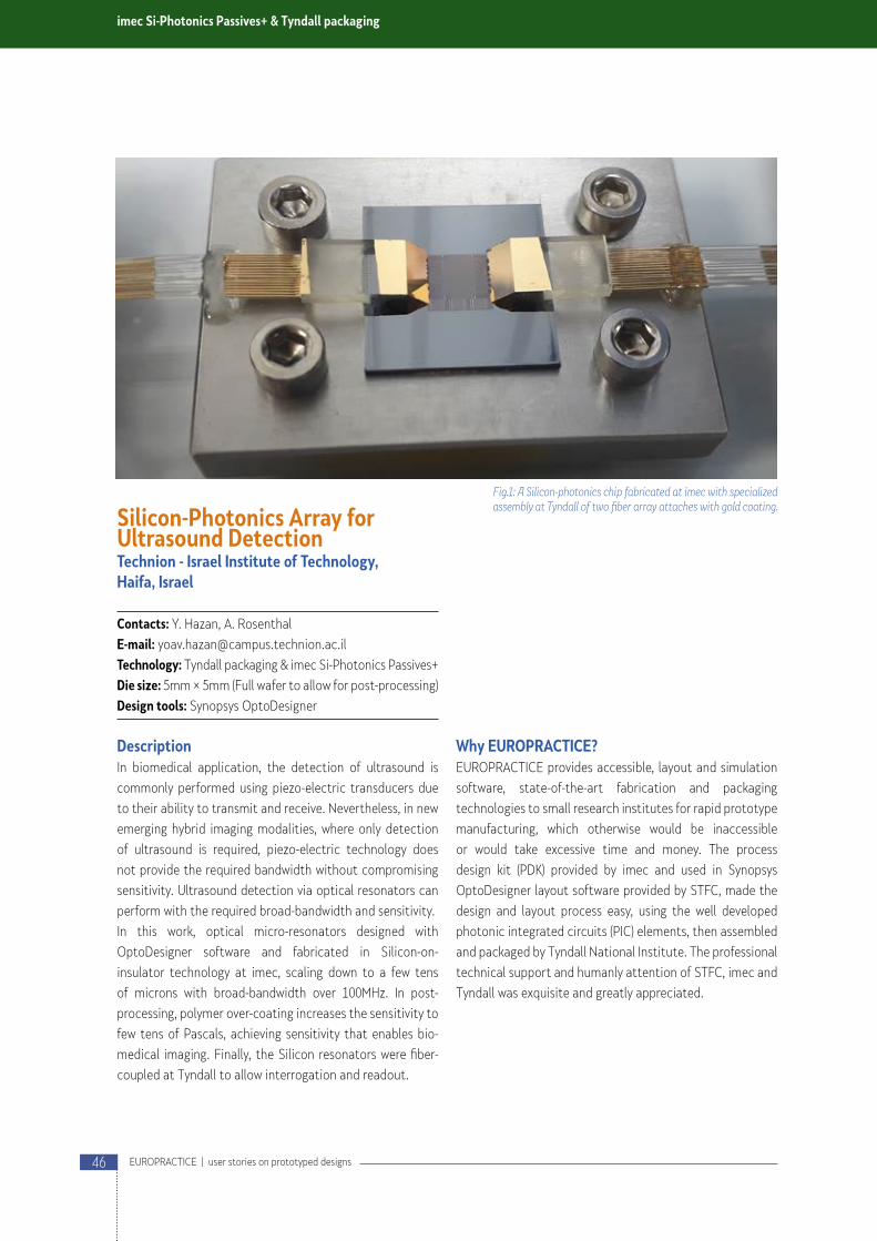
Silicon-Photonics Array for Ultrasound DetectionTechnion - Israel Institute of Technology, Haifa, Israel
Contacts: Y. Hazan, A. Rosenthal
E-mail: [email protected]
Technology: Tyndall packaging & imec Si-Photonics Passives+
Die size: 5mm × 5mm (Full wafer to allow for post-processing)
Design tools: Synopsys OptoDesigner
DescriptionIn biomedical application, the detection of ultrasound is
commonly performed using piezo-electric transducers due
to their ability to transmit and receive. Nevertheless, in new
emerging hybrid imaging modalities, where only detection
of ultrasound is required, piezo-electric technology does
not provide the required bandwidth without compromising
sensitivity. Ultrasound detection via optical resonators can
perform with the required broad-bandwidth and sensitivity.
In this work, optical micro-resonators designed with
OptoDesigner software and fabricated in Silicon-on-
insulator technology at imec, scaling down to a few tens
of microns with broad-bandwidth over 100MHz. In post-
processing, polymer over-coating increases the sensitivity to
few tens of Pascals, achieving sensitivity that enables bio-
medical imaging. Finally, the Silicon resonators were fiber-
coupled at Tyndall to allow interrogation and readout.
Why EUROPRACTICE?EUROPRACTICE provides accessible, layout and simulation
software, state-of-the-art fabrication and packaging
technologies to small research institutes for rapid prototype
manufacturing, which otherwise would be inaccessible
or would take excessive time and money. The process
design kit (PDK) provided by imec and used in Synopsys
OptoDesigner layout software provided by STFC, made the
design and layout process easy, using the well developed
photonic integrated circuits (PIC) elements, then assembled
and packaged by Tyndall National Institute. The professional
technical support and humanly attention of STFC, imec and
Tyndall was exquisite and greatly appreciated.
imec Si-Photonics Passives+ & Tyndall packaging
Fig.1: A Silicon-photonics chip fabricated at imec with specialized assembly at Tyndall of two fiber array attaches with gold coating.
46 EUROPRACTICE | user stories on prototyped designs

Design of High-speed Multi-lane Silicon Photonics MZM arrayDepartment of Micro/Niao Electronics, Shanghai Jiao Tong University, China
Contact: Prof. Sun Yanan
E-mail: [email protected]
Technology: imec Si-Photonics IsiPP50G
Die size: 5150μm × 5150μm
IntroductionSilicon photonics is becoming the technology of choice for
optical transceivers in short reach optical interconnect
systems. It leverages the existing microelectronic fabrication
infrastructures, promising lower fabrication cost and larger
scale integration than III-V photonics. To meet the performance
requirement in bandwidth density and cost in next-generation
high-performance computers and data centers, it is critical
to achieve high-density integration of optical transceivers.
However, using the principle of parallelism and scale-out
the channel count, the large footprint and spacing of driving
electrodes limit the bandwidth density. To overcome this
limitation, a more compact device footprint and greater
flexibility design is quite necessary.
DescriptionThis work implemented a high-density and high-speed
multi-lane traveling wave MZM array based on imec silicon
photonics technology. We proposed a novel compact
traveling-wave electrode structure for the MZM, and
shared the ground pad between two neighboring MZMs
to reduce the device size. Two MZM arrays with different
lengths are designed in this chip. The optical eye-diagram
measurement results show that MZM array can work at
25Gbps simultaneously with low crosstalk.
Why EUROPRACTICE?The EUROPRACTICE provides accessible access to foundry
services to research institutions that could otherwise not easily
support regular fabrication costs. We have been working with
EUROPRACTICE many years. In this work, we used imec silicon
photonics technology ISiPP50G offered by the MPW service of
EUROPRACTICE. We really appreciated EUROPRACTICE and
imec technical support at every step of the chip design process,
which significantly speeded up the development of the chip.
imec Si-Photonics IsiPP50G
Fig.1: Photograph of the fabricated die.
Fig.2 Optical eye diagrams of Tx channels at single-ch operation and simultaneously at all 4-ch operations.
47EUROPRACTICE | user stories on prototyped designs

Compact arrayed waveguide grating spectrometer for spectral-domain optical coherence tomography at 860 nm center wavelength on silicon nitride platformCenter for Advanced Research in Photonics, Department of Electronic Engineering, The Chinese University of Hong Kong, Hong Kong
Contact: Hon Ki Tsang
E-mail: [email protected]
Technology: imec SiN-Photonics BioPIX300
Die size: 10.75mm × 4.75mm
Description The spectral domain optical coherence tomography (SD-OCT)
is a three-dimensional (3D) imaging technique which obtain
the information of the sample in depth direction by measuring
the interference signal in spectral domain. A broadband and
high-resolution spectrometer is the key component in SD-OCT
system, which guarantees the large imaging depth and high
imaging resolution in depth direction. Silicon nitride platform,
with wide transparent spectral range, enables the operation
of the spectrometer at the 860 nm center wavelength, which
is often the spectral region of choice for in-vivo bio-imaging.
We designed a 40-channel arrayed waveguide grating (AWG)
spectrometer with 60 nm operating bandwidth and 1.5 nm
spectral resolution.
Enabled by the high professional MPW service from imec
under the PIX4life silicon nitride MPW, and especially with the
high-quality devices fabricated, the AWG spectrometer we
designed showed 1.3 dB experimental insertion loss and about
-20 dB inter-channel crosstalk with experimental spectral
resolution and optical bandwidth exactly matching with the
design value. The total footprint of the AWG spectrometer is
910μm × 680μm. This AWG spectrometer with relatively good
performance on silicon nitride also enabled our publication
“Ultracompact 40-Channel Arrayed Waveguide Grating on
Silicon Nitride Platform at 860 nm,” IEEE Journal of Quantum
Electronics 56, 8400308 (2020).
Another paper has been submitted discussing the limitations on
crosstalk performance in large-scale arrayed waveguides from
the phase variations caused by nitride thickness nonuniformity
and how alternative approaches can alleviate this problem for
high resolution and wide optical bandwidth spectrometers.
The MPW service has also helped us to gain further research
grant funding from Hong Kong government for developing
integrated spectrometers for advanced dynamic optical
coherence tomography.
PIX4life and EUROPRACTICEImec SiN-Photonics was developed within PIX4life, a
European open-access pilot line for Photonic Integrated
Circuits (PICs) targeting life science applications in the
visible range. PIX4life services are available through
EUROPRACTICE.
imec SiN-Photonics BioPIX300
Fig.1: Microscope image of the 40-channel AWG spectrometer.
Fig.2: SEM image of parabolic tapers in the AWG spectrometer.
Fig.3: Experimental transmission spectrum of the AWG spectrometer.
48 EUROPRACTICE | user stories on prototyped designs

A Primary Study of Electrostatic Actuated Switch using the Technology of PiezoMUMPsDepartment of Microelectronics and Nanoelectronics, University of Malta, Malta
Contact: Mounira Bengashier
E-mail: [email protected]
Technology: PiezoMUMPs
Die size: 11.15mm × 11.15mm
Design tools: CoventorWare
DescriptionA number of non-contact electrostatic actuated switches were
designed using the PiezoMUMPs technology and submitted to
EUROPRACTICE for fabrication. These switches are of different
designs and having various geometries in order to analyse and
minimise the Pullin voltage. This work is part of a Ph.D. research
study on the design of piezoelectric tuneable MEMS lateral bulk
acoustic wave resonators originally based on the thermal effect
on the resonant frequency in order to explore the feasibility of
fine frequency tuning. The possibility of fine tuning can be applied
to high precision timing circuits such as frequency counters. The
possibility of having a switchable array of different resonators in
the same chip results in a cost-effective wider frequency range.
These non-contact electrostatic switches were analytically
studied and simulated using CoventorWare FEM.
Proposed Design GeometryThe switch was fabricated using MEMSCAP’s PiezoMUMPs
Process. Figure 1 shows the first designed switch including the
shape of one of the 4 springs having the following dimensions:
Signal line, movable electrode gaps are 3,9 μm, Signal line,
movable electrode Overlap is 110 μm, Gap between two
actuation electrodes is 11.5 μm, Switch’s geometry (W, L, T) are
(320, 500,10) μm. The simulated pull-in voltage for designs having
a different number of comb fingers obtained using CoventorWare
FEM analyser tool are also shown in Figure 1. The pull-in voltage
was further reduced to 21 V by reducing the spring stiffness. This
was achieved by changing the spring geometry, having a length
and width of 160 μm and 24 μm respectively.
Why EUROPRACTICE? The EUROPRACTICE service offers affordable simple
procedures to access the technology to produce MEMS
prototypes for research purposes, and this service is always
open to provide support and answer questions regarding
technical issues encountered by the users.
Acknowledgement We would like to acknowledge the Ministry of High Education
in Libya for supporting the Ph.D. research work of Mounira
Bengashier, which is currently being carried out at the
Department of Microelectronics and Nanoelectronics at the
University of Malta.
MEMSCAP PiezoMUMPs
Fig.1: Design layouts for different 3-state non-contact Switches with varying comb lengths, including Spring details and pull-in Voltage simulated by Finite Element Analysis (FEA).
Fig.2: The final selected 3-state non-contact Switch connected to a PiezoMUMPs resonator.
49EUROPRACTICE | user stories on prototyped designs

Z-axis MEMS Accelerometer for Vibrotactile Display PadDepartment of Electronic and Electrical Engineering, University of Bath, UK
Contacts: Dr Ali Mohammadi, Mr Steven Ng
E-mail: [email protected]
Technology: X-FAB MEMS XMB10
Die size: 4mm × 2.5mm
Design tools: Coventor MEMS+, Cadence
DescriptionAssistive technologies such as Braille and swell papers have
been evolved to digital tactile displays, which help the visually
impaired (VI) individuals to receive graphical information
through the sense of touch. At the University of Bath, we
have developed a new high-resolution vibrotactile display
technique [1] following the feedback received from researchers
in the Departments of Computer Science, Psychology and
Education. Our technique allows one electromagnetic coil to
selectively vibrate multiple smaller tactile pixels (taxels) based
on their mechanical resonance frequency. This technique
mitigates the resolution bottleneck of existing tactile displays.
We now investigate the integration of tactile sensing
mechanism in the new actuator to control the vibration of
tactile elements. This sensor will allow the implementation
of a closed-loop control system to accurately track the
resonance frequency of taxels. In addition, the proposed
sensor will create an interactive and bilateral communication
to receive tactile input from the user.
Thereby, we have embedded off-the-shelf piezoelectric sensors
underneath the taxels to track the resonance frequency of
the taxels. However, the bulky size of these sensors avoids
using individual sensors especially in the high-resolution taxel
configuration, whereby multiple taxels are implemented within
a small area. In this project, we have designed capacitive MEMS
sensors in XFAB processes to measure the vibration of 3D printed
taxels. The capacitive sensors built in XMB10 processes will
measure the displacement of taxels in Z direction and supply the
measured output as the feedback signal to the actuator input.
References[1] A. Mohammadi, M. Abdelkhalek, and S. Sadrafshari, “Resonance frequency
selective electromagnetic actuation for high-resolution vibrotactile displays,”
Sensors and Actuators A: Physical, vol. 302, p. 111818, 2020.
Acknowledgement to EUROPRACTICE and X-FABEUROPRACTICE microfabrication and software services helped
us to establish a new line of research in Microelectromechanical
Systems (MEMS) at University of Bath. We highly appreciate
the availability of technical guidance and expertise, choice of
reliable microfabrication process technologies, and reasonable
prices – all provided by EUROPRACTICE. The training programs
for software and webinars for process technologies are extremely
useful services. This project was specifically supported by the
X-FAB and EUROPRACTICE MEMS Design Award in 2020.
X-FAB XMB10 MEMS DESIGN CONTEST: FIRST PLACE
Fig.2: The proof mass deflection in the heavier side is larger than the lighter side, which is needed for measuring out-of-plane acceleration.
Fig.1: SEM image of the z-axis accelerometer with comb finger capacitive transducers for sensing and actuation purposes.
Fig3: Harmonic analysis in Coventor MEMS+ shows the resonant modes in X, Y and Z direction.
50 EUROPRACTICE | user stories on prototyped designs

A scanning diffraction grating for high performance gas sensing applicationsUniversity of Malta - Department of Microelectronics and Nanoelectronics, Msida, Malta
Designer: Russell Farrugia
Supervisor: Prof. Ivan Grech, Prof. Joseph Micallef
E-mail: [email protected]
Technology: X-FAB MEMS XMB10
Die size: 4.5mm × 2.2mm
Design tools: CoventorWare
IntroductionThe University of Malta is currently developing an infrared
Czerny-Turner spectrometer for multi-gas detection. In the
spectrometer design of Figure 1, a collimated broadband IR
source is directed towards a diffraction grating. The diffracted
beam is then focused on to the detector plane using an imaging
mirror. The spectral image is typically measured using an
expensive linear photodetector array. The latter can be replaced
by a single element photodetector with the implementation
of a MEMS scanning diffraction grating. The design of a novel
MEMS scanning grating was fabricated using the XFAB XMB10
process. Figure 2 depicts the layout of the 2.2 mm × 4.5 mm chip.
The MEMS scanning grating enables the realization of a compact
IR spectrometer for high speed, high resolution gas spectral
analysis and eliminates the problems of cross-sensitivity and
decay which characterize metal oxide gas sensors.
DescriptionThe scanning grating of Figure 3 is designed to oscillate at a
torsional out-of-plane resonant mode at a frequency of 2 kHz.
The resonating micro-scanner is driven by angular vertical comb
drive structures. The electrostatic and mirror plate structures
are etched from the 30μm silicon device layer. A lamellar grating
pattern is formed using the 5μm deep DRIE process step, typically
intended for the fabrication of comb fingers with a reduced
height. The aluminum layer, intended for wiring and bond pad
metallization is considered in order to improve the reflectivity of
the grating pattern. The scanning mirror plate is supported on
either side by dual torsion beam structures. The torsion beams
are optimized such that the torsional stiffness is minimized,
and the lateral and out-of-plane bending stiffness is maximized.
Lateral springs are also included in the scanning grating design to
provide a degree of compliance against external forces along the
rotational axis. Moreover, stoppers are added to the end of the
torsion beams to limit excessive out-of-plane rotation.
Why EUROPRACTICE?EUROPRACTICE provides doctoral students, researchers
and academics with access to state-of-the-art MPW foundry
services for the fabrication of MEMS/MOEMS device
prototypes. The University of Malta has always been provided
with the necessary technical feedback and expertise at every
stage of the chip design process.
AcknowledgementsThe authors would like to acknowledge imec/EUROPRACTICE
for their support through the MEMS Design Contest for Users of
chip design in X-FAB XMB10 technology and Malta Enterprise
for their financial support as part of the PENTA project ESAIRQ.
X-FAB XMB10 MEMS DESIGN CONTEST: SECOND PLACE
Fig.1: Czerny-Turner Spectrometer prototype design.
Fig.2: Layout of the fabricated chip.
Fig.3: SEM image of the indirect-drive resonant micro-mirror.
51EUROPRACTICE | user stories on prototyped designs

Silicon MEMS comb-drive actuators for strain engineering Dept. of Precision and Microsystems Engineering, Delft University of Technology, the Netherlands
Contacts: Satadal Dutta, Peter G. Steeneken, Gerard J. Verbiest
E-mail: [email protected]
Technology: X-FAB MEMS XMB10
Die size: 3mm × 3mm
Design tools: Coventor MEMS+
DescriptionWe designed a set of electrostatic comb drive actuators (Figs.
1, 2a) and piezo resistive MEMS actuators (Fig. 2b) in silicon,
with varying configurations and geometry. These can be used
to gain strain control in suspended metallic or semiconducting
membranes for static as well as dynamic excitations. These are
beneficial for the development of new sensors and increasing the
outreach of standard silicon MEMS technology.
Micro-machined comb-drive (CD) actuators have been developed
in the last years from highly p-doped silicon, which allows low-
temperature operation [1][2]. The actuators are intended to be
driven differentially to increase the range of linearity between
small signal force and displacement. The XMB10 process allowed
us to place silicon membranes of recessed height (in the vertical
axis), which enabled us to integrate a vertical electrostatic gate
with an air gap of 5μm. The strong bending thickness of the active
layer allows us to gently push on the suspended comb without
destroying it (Fig. 1). The relatively high p-doping is beneficial for
the combs to be actuated both at room temperature and also at
around liquid nitrogen temperature. An important parameter is
the stroke of the interdigitated fingers. We need enough stroke
to induce a few percent of strain in a membrane longer than
10 microns. The meshed design of the movable comb (Figs. 1,
2a) helps in reducing the inertial mass and thus increasing the
stroke in the lateral direction. Further, we opted not to include
the capping wafer during fabrication, and the yield of our devices
was still very good (> 95 %). The exceptions were four broken
devices with spring-structures of very high lateral aspect ratio
(> 20). Various configurations of comb-drive actuators were
implemented which can be used to generate both shear (uniaxial,
radial) and torsional strain on the plane of the die. The process
includes ohmic contacts to silicon, which allowed us to design
piezo-resistive MEMS actuators, in the form of silicon loops
connecting two bond pads (Fig. 2b), with the thinnest finger
with being 2 μm. The simulated fundamental eigenfrequency
of the movable comb in our design was 39.15 kHz, with a total
displacement of 0.15 μm for a bias of 10 V at 300 K.
Why EUROPRACTICE?The EUROPRACTICE makes it easier and affordable for academia
to access a wide range of foundry services under a common um-
brella. The active design support is also valuable for research. The
available component library of XMB10 and its consolidated pro-
cess design kit with 3D design software such as Coventor MEMS+
helps the researchers to simplify and to improve the prototyping
of active and passive devices by ensuring final top-quality.
AcknowledgmentWe would like to thank the Plantenna research programme funded
by the 4TU federation.
References[1] M. Goldsche, J. Sonntag, et al., Nano Lett., vol. 18, no. 3, pp. 1707–1713, 2018.[2] M. Goldsche, G. J. Verbiest, et al., Nanotechnology vol. 29, no. 37, 375301, 2018.
X-FAB XMB10 MEMS DESIGN CONTEST: THIRD PLACE
Fig.1: (a) Top-view micrograph of the fabricated comb-drive actuator, with zoom-in on some finer features (interdigitated combs, springs, and stepped electrostatic gate region). (b) 3D device layout using XMB10 PDK in CoventorWare MEMS+. The software supports mask generation from the in-built process module.
Fig. 2: Top-view die micrographs of (a) a variant of the comb drive actuator and (b) the piezo-resistive MEMS actuators.
52 EUROPRACTICE | user stories on prototyped designs

AlgeriaR21350 Centre Algérien de Développement des Technologies Avancées
AustriaA00500 Fachhochschule KärntenA13020 Fachochschulstudiengange OberösterreichA13470 Technische Universität Wien Institute of TelecommunicationsA14240 Fachhochschule Techhnikum WienA14480 Fachhochschule JoanneumA15350 Fachhochschule Wiener NeustadtA15640 Universität InnsbruckA15880 Johannes Kepler Universität Linz - NTHFSA15980 Höhere Technische Bundeslehr- und Versuchsanstalt RankweilA35090 Technische Universität WienA36470 Technische Universität GrazA38430 Johannes Kepler Universität LinzR21070 AIT Austrian Institute of TechnologyR21210 Österreichische Akademie der Wissenschaften - WienR21590 Österreichische Akademie der Wissenschaften - GrazR22510 Silicon Austria Labs GmbH (Villach)R22520 Silicon Austria Labs GmbH (Linz)
BelarusA47550 Belarusian State UniversityA47630 Belarusian State University of Informatics and
Radioelectronics
BelgiumA13940 Université de LiègeA35651 Université Catholique de LouvainA35880 Universiteit GentA37190 Universiteit AntwerpenA37210 Vrije Universiteit BrusselA37220 Katholieke Universiteit LeuvenA38160 Université de MonsA38190 Université Libre de BruxellesR00040 imecR21440 Studiecentrum voor Kernenergie - Centre d'Etude de l'énergie
Nucléaire
EUROPRACTICE MEMBERSHIPTogether with the funding provided by the
European Commission, EUROPRACTICE needs
additional support to provide high quality service
to more than 600 European universities and
research institutes. Membership Fees pay for
extra staff supporting this requested stimulation
activity for academic institutions (not fully paid by
the EU). The annual Membership Fee is collected
by STFC on behalf of the EUROPRACTICE project
partners.
European universities and research institutes can
choose from 4 different levels of membership:
1. Full-IC annual membership: 1.100 €
Allowing full access to all CAD tools, Design
Kits and Libraries, MPW fabrication, mini@ sic
runs at reduced prices. This membership fee
is split 600 € for the CAD part (including 100 €
to administer the membership) and 500 € for
the prototyping part.
2. MPW-only annual membership: 600 €
Allowing full access to all offered MPW runs
at discounted pricing.
3. Design tool only annual membership: 600 €
Allowing full access to all the offered CAD
tools only.
4. FPGA-only annual membership: 200 €
Allowing access to FPGA tools only e.g.
Altera, Xilinx, and Synopsys Synplify.
The number of academic members consists
of more than 600 institutes in more than
40 countries from the EMEA zone (Europe, Middle
East and Africa).
EUROPRACTICE MEMBERSHIP LIST PER COUNTRY
53EUROPRACTICE | list of members
Bosnia and HerzegovinaA48180 Univerzitet u Banjoj Luci
BulgariaA40090 Technical University of Sofia
CroatiaA47680 Sveuciliste u ZagrebuA47920 Sveuciliste J.J. StrossmayeraA48090 Sveuciliste u Splitu
CyprusA07090 University of Cyprus
Czech RepublicA40060 Ceske vysoke uceni technicke v PrazeA40070 Vysoke uceni technicke v BrneR22660 Institute of Organic Chemistry and BiochemistryR47460 Akademie ved Ceske republikyR49000 Ustav teorie informace a automatizace AV CR
DenmarkA13030 Københavns UniversitetA15510 Aarhus UniversitetA35060 Aalborg UniversitetA36040 Danmarks Tekniske Universitet
EgyptA14550 Ain Shams UniversityA14670 Cairo UniversityA15090 The German University in CairoA15160 The American University in CairoA15170 Egypt-Japan University of Science & TechnologyA16020 Zewail City of Science & TechnologyR22620 Electronics Research Institute
EstoniaA40110 Tallinna Tehnikaülikool
FinlandA15740 Satakunnan ammattikorkeakouluA35040 Aalto-yliopistoA35610 Tampereen teknillinen yliopistoA35820 Oulun yliopistoA39360 Turun yliopistoR14360 Fysiikan tutkimuslaitosR21240 VTT Technical Research Centre of Finland
FranceA00100 Institut Supérieur de l'Aéronautique et de l'EspaceA13800 Université de LorraineA14440 Laboratoire de Physique Corpusculaire de CaenA16400 Ecole Nationale Superieure des TechniquesA16510 École Supérieure d'Ingénieurs en Genie ElectriqueA35020 Sorbonne UniversitéA35290 Université de Montpellier 2A35800 JUNIA - Etablissement ISEN-LilleA36061 Centre Interuniversitaire de Microélecronique et de
NanotechnologiesA36311 Institut National des Sciences Appliquées de LyonA36312 École Supérieure de Chimie Physique Électronique de LyonA36410 Atelier Interuniversitaire de MicroélecroniqueA37470 Université de StrasbourgA37590 Aix Marseille UniversitéA37670 Laboratoire de Physique Nucléaire et de Hautes EnergiesA37710 IMT Atlantique Bretagne-Pays de la LoireA37950 Institut de Physique des 2 Infinis de LyonA37980 Université Joseph FourierA39060 Laboratoire d'Annecy-le-Vieux de physique des particules
A39400 Université Clermont AuvergneR00210 Laboratoire d'Analyse et d'Architectures des SystèmesR14140 Laboratoire des sciences de l'ingénieur, de l'informatique et
de l'imagerieR15140 XLIM Université de LimogesR20490 European Synchrotron Radiation FacilityR20810 Station de Radioastronomie de Nançay, Observatoire de
ParisR20980 Laboratoire des Plasmas et de Conversion d'EnergieR21010 Laboratoire de Physique et Chimie de l'Environnement et de
l'EspaceR21020 Synchrotron SOLEILR21030 Institut Matériaux Microélectronique Nanosciences de
ProvenceR21140 Institut Laue-LangevinR21170 Laboratoire de l'Accélérateur LinéaireR21270 Commissariat à l'énergie atomique et aux énergies
alternatives - IRFUR21290 Spintronique et Technologie des Composants R21380 Laboratoire de Physique des PlasmasR21560 Office National d'Études et de Recherches Aérospatiales -
ToulouseR21960 Institut de recherche en astrophysique et planétologieR22060 Institut d'Astrophysique SpatialeR22210 Centre de Microélectronique OMEGAR22220 Commissariat à l'énergie atomique et aux énergies
alternatives - LETI DACLER22280 Institut de Recherche sur les Composants logiciels et
matériels pour l’Information et la Communication AvancéeR22310 Grand Accélérateur National d'Ions LourdsR22360 Institut de Recherche et Technologie Antoine de Saint
ExupéryR22590 Circuits Multi-ProjetsR22680 Institut des Sciences Chimiques de RennesR37850 Laboratoire de Physique des 2 Infinis Irène Joliot-CurieR38290 Laboratoire de l'Intégration du Matérieu au Système
GermanyA00110 Johannes Gutenberg Universität MainzA00240 Fachhochschule KölnA00510 Hochschule Konstanz für Technik, Wirtschaft und GestaltungA00670 Hochschule BremenA00850 Justus Liebig-Universität GießenA12140 Technische Universität München - Fakultät für Physik
(Garching)A12270 Hochschule Albstadt-SigmaringenA12410 Fachhochschule SchmalkaldenA12440 Hochschule PforzheimA12540 Brandenburgische Technische Universität CottbusA12840 Bergische Universität WuppertalA13060 Albert-Ludwigs-Universität Freiburg - IMTEKA13610 Fachhochschule AachenA13650 Technische Universität Darmstadt - Institut für
Halbleitertechnik und Nanoelektronik (IHT)A13660 Universität Bremen - InformatikA13680 Technische Hochschule AschaffenburgA13890 Technische Universität Berlin - Institut für Technische
Informatik und Mikroelektronik (TIME)A14130 Fachhochschule BrandenburgA14310 Universität Kassel - Fachbereich Elektrotechnik/InformatikA14740 Universität KasselA14920 Universität KonstanzA15030 Universität BielefeldA15230 Hochschule für Angewandte Wissenschaften HamburgA15330 Carl von Ossietzky Universität Oldenburg - Energie und
Halbleiterforschung (EHF)
54 EUROPRACTICE | list of members
A15410 Technische Hochschule Mittelhessen - FriedbergA15500 Hochschule RheinMainA15840 Hochschule RosenheimA15930 Fachhochschule SüdwestfalenA15950 Beuth Hochschule für Technik BerlinA16030 Rheinisch-Westfälische Technische Hochschule Aachen -
Lehrstuhl für Integrierte Photonik (IPH)A16040 Rheinisch-Westfälische Technische Hochschule Aachen -
Institut für Stromrichtertechnik und Elektrische Antriebe (ISEA)
A16060 Rheinisch-Westfälische Technische Hochschule Aachen - Institut für Theoretische Elektrotechnik (ITHE)
A16090 Westfälische HochschuleA16100 Hochschule fuer Technik und Wirtschaft Berlin (HTW Berlin)A16310 Technische Universität Bergakademie FreibergA16320 RWTH Aachen, Physikalisches Institut BA16330 Hochschule HannoverA16450 Universität MannheimA16490 Universität BayreuthA16520 Westfälische Wilhelms-UniversitätA16590 IUBH University of Applied SciencesA35320 Technische Universität Hamburg-HarburgA35400 Hochschule UlmA35420 Georg-Simon-Ohm Hochschule NürnbergA35430 Karlsruher Institut für TechnologieA35450 Technische Universität Darmstadt - Integrierte Elektronische
Systeme (IES)A35500 Eberhard Karls Universität TübingenA35590 Johannes-Wolfgang-Goethe-Universität Frankfurt am MainA35600 Technische Universität Carolo-Wilhelmina zu BraunschweigA35620 Universität Bremen - Institut für Theoretische Elektrotechnik
und MikroelektronikA35640 Rheinisch-Westfälische Technische Hochschule Aachen -
Institute for Communication Technologies and Embedded Systems (ICE)
A35710 Hochschule AugsburgA35810 Technische Universität KaiserslauternA35830 Universität HamburgA35990 Universität Duisburg-EssenA36070 Carl von Ossietzky Universität Oldenburg - InformatikA36440 Universität des SaarlandesA37090 Technische Universität DortmundA37240 Hochschule FurtwangenA37290 Leibniz Universität HannoverA37310 Technische Universität BerlinA37380 Friedrich-Alexander-Universität Erlangen-NürnbergA37390 Technische Universität München - Fakultät für
Elektrotechnik und Informationstechnik MünchenA37440 Universität der Bundeswehr MünchenA37450 Hochschule EsslingenA37500 Universität PaderbornA37510 Hochschule für Angewandte Wissenschaften MünchenA37530 Humboldt-Universität zu BerlinA37540 Universität UlmA37760 Technische Universität DresdenA37800 Hochschule OffenburgA37810 Rheinisch-Westfälische Technische Hochschule Aachen -
Fakultät für Elektrotechnik und InformationstechnikA37880 Hochschule AalenA37920 Hochschule Ravensburg-WeingartenA37930 Hochschule MannheimA38010 Hochschule HeilbronnA38030 Hochschule DarmstadtA38080 Ruhr-Universität BochumA38090 Otto-von-Guericke-Universität MagdeburgA38220 Universität Siegen
A38240 Technische Universität IlmenauA38340 Technische Universität ChemnitzA38550 Ostfalia Hochschule für angewandte WissenschaftenA38650 Fachhochschule DortmundA38890 Rheinische Friedrich-Wilhelms-Universität BonnA38940 Ernst-Abbe-Fachhochschule JenaA39000 Technische Hochschule Mittelhessen - GießenA39070 Hochschule Karlsruhe - Technik und WirtschaftA39110 Universität StuttgartA39220 Universität RostockA39250 Ruprecht-Karls-Universität Heidelberg - ASICA39260 Albert-Ludwigs-Universität FreiburgA39330 Hochschule ReutlingenA39340 Martin-Luther-Universität Halle-WittenbergA39460 Christian-Albrechts-Universität zu KielA39580 Hochschule OsnabrückA39660 Friedrich-Schiller-Universität JenaA39770 Universität zu LübeckR00150 Max-Planck-Institut für PhysikR20300 Institut für Mikroelektronik- und Mechatronik - Systeme
gemeinnützige GmbHR20330 Deutsches Elektronen-SynchrotronR20460 Institut für Mobil- und Satellitenfunktechnik GmbHR20510 IHP GmbH - Leibniz-Institut für innovative MikroelektronikR20720 Oldenburger Forschungs- und Entwicklungsinstitut für
Informatik-Werkzeuge und -SystemeR20880 GSI Helmholtzzentrum für Schwerionenforschung GmbHR20890 Fraunhofer-Institut für SiliziumtechnologieR20900 Fraunhofer-Institut für Biomedizinische TechnikR20920 Fraunhofer-Institut für Integrierte Schaltungen - ErlangenR20930 Fraunhofer-Institut für Integrierte Schaltungen - DredenR21050 Max-Planck-Institut für ChemieR21060 Forschungszentrum JülichR21090 Fraunhofer Heinrich-Hertz-InstitutR21120 Max-Planck-Institut für extraterrestrische PhysikR21150 Physikalisch-Technische Bundesanstalt - BraunschweigR21220 Fraunhofer-Institut für Integrierte Systeme und
BauelementetechnologieR21260 Hochschule für Technik und Wirtschaft DresdenR21310 Fraunhofer-Institut für Photonische MikrosystemeR21320 Fraunhofer-Institut für Solare EnergiesystemeR21510 Deutsches Zentrum für Luft- und Raumfahrt - BerlinR21530 Deutsches Zentrum für Luft- und Raumfahrt - BremenR21580 Deutsches Zentrum für Luft- und Raumfahrt IIP - BerlinR21610 Helmholtz-Zentrum Berlin für Materialien und EnergieR21620 Fraunhofer-Einrichtung für Angewandte und Integrierte
SicherheitR21630 Fraunhofer-Institut für Zerstörungsfreie PrüfverfahrenR21650 Fraunhofer-Institut für Hochfrequenzphysik und
RadartechnikR21660 Fraunhofer-Einrichtung für Systeme der
KommunikationstechnikR21770 Konrad-Zuse-Zentrum für Informationstechnik BerlinR21780 Deutsches Zentrum für Luft- und Raumfahrt - WesslingR21790 NaMLab gGmbHR21900 Max-Planck-Institut für RadioastronomieR21970 PNSensor gGmbHR22020 European XFELR22080 Fraunhofer Institute for Organic Electronics, Electron Beam
and Plasma Technology FEPR22110 Physikalisch-Technische Bundesanstalt - BerlinR22150 Fraunhofer Institute SITR22160 Halbleiterlabor der Max Planck GesellschaftR22260 Helmholtz-Zentrum GeesthactR22290 Fraunhofer-Einrichtung für Mikrosysteme und Festkörper-
Technologien EMFT
55EUROPRACTICE | list of members
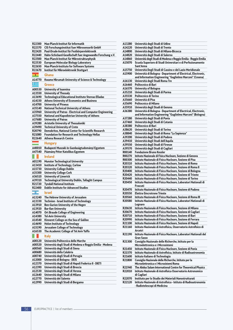
R22300 Max-Planck-Institut für InformatikR22370 CIS Forschungsinstitut fuer Mikrosensorik GmbHR22420 Paul-Drude-Institut für FestkörperelektronikR22440 Hahn-Schickard-Gesellschaft fuer Angewandte Forschung e.V.R22500 Max-Planck-Institut für MikrostrukturphysikR22530 European Molecular Biology LaboratoryR22650 Max-Planck-Institute for Software SystemsR22670 Institut für Mikroelektronik Stuttgart
GhanaA14770 Kwame Nkrumah University of Science & Technology
GreeceA00530 University of IoanninaA13550 University of ThessalyA13690 Technological Educational Institute Stereas ElladasA14150 Athens University of Economics and BusinessA14700 University of PiraeusA35140 National Technical University of AthensA35960 University of Patras - Electrical and Computer EngineeringA37550 National and Kapodistrian University of AthensA37680 University of PatrasA39280 Aristotle University of ThessalonikiA39490 Technical University of CreteR20790 Demokritos, National Center for Scientific ResearchR21080 Foundation for Research and Technology HellasR22640 Athena Research Centre
HungaryA40010 Budapesti Muszaki és Gazdaságtudományi EgyetemA47540 Pázmány Péter Katolikus Egyetem
IrelandA01190 Munster Technological UniversityA13410 Institute of Technology, CarlowA15730 University College DublinA35300 University College CorkA36510 University of LimerickA39310 Technological University Dublin, Tallaght CampusR21720 Tyndall National InstituteR22400 Dublin Institute for Advanced Studies
IsraelA13240 The Hebrew University of JerusalemA13330 Technion - Israel Institute of TechnologyA13910 Ben-Gurion University of the NegevA13920 Bar-Ilan UniversityA14070 Ort Braude College of EngineeringA14380 Tel-Aviv UniversityA14540 Kinneret College on the Sea of GalileeA14690 Holon Institute of TechnologyA15190 Jerusalem College of TechnologyA16530 The Academic College of Tel Aviv Yaffo
ItalyA00120 Università Politecnica delle MarcheA00520 Università degli Studi di Modena e Reggio Emilia - ModenaA00560 Università degli Studi di SienaA00680 Università della CalabriaA00740 Università degli Studi di PerugiaA12000 Università di Bologna - DEISA12370 Università degli Studi di Napoli Federico II - DIETIA12390 Università degli Studi di BresciaA12530 Università degli Studi di VeronaA12640 Università degli Studi di MilanoA12770 Università del SalentoA12990 Università degli Studi di Bergamo
A13280 Università degli Studi di UdineA14220 Università degli Studi di TrentoA14800 Università degli Studi di Milano-BicoccaA14820 Università degli Studi di SalernoA14860 Università degli Studi di Modena e Reggio Emilia - Reggio EmiliaA15070 Scuola Superiore di Studi Universitari e di Perfezionamento
Sant'AnnaA15750 Università Degli Studi di Cassino e del Lazio MeridionaleA15900 Università di Bologna - Department of Electrical, Electronic,
and Information Engineering "Guglielmo Marconi" (Cesena)A16130 Università degli Studi Roma TreA16460 Politecnico di BariA16570 University of BolognaA35210 Università degli Studi di ParmaA35530 Politecnico di TorinoA35660 Università di PisaA35690 Politecnico di MilanoA35910 Università degli Studi di GenovaA36380 Università di Bologna - Department of Electrical, Electronic,
and Information Engineering "Guglielmo Marconi" (Bologna)A37280 Università degli Studi di PaviaA37460 Università degli Studi di CataniaA38380 Politecnico di BariA38620 Università degli Studi di TorinoA38840 Università degli Studi di Roma "La Sapienza"A39200 Università degli Studi di PadovaA39410 Università degli Studi dell'AquilaA39550 Università degli Studi di FirenzeA39570 Università degli Studi di CagliariR00140 Fondazione Bruno KesslerR00270 Istituto Nazionale di Fisica Nucleare, Sezione di GenovaR00300 Istituto Nazionale di Fisica Nucleare, Sezione di PisaR20310 Istituto Nazionale di Fisica Nucleare, Sezione di RomaR20320 Istituto Nazionale di Fisica Nucleare, Sezione di Roma IIR20400 Istituto Nazionale di Fisica Nucleare, Sezione di BolognaR20420 Istituto Nazionale di Fisica Nucleare, Sezione di TriesteR20440 Istituto Nazionale di Fisica Nucleare, Sezione di TorinoR20450 Istituto Nazionale di Fisica Nucleare, Laboratori Nationali di
FrascatiR20470 Istituto Nazionale di Fisica Nucleare, Sezione di PadovaR20550 Elettra-Sincrotrone TriesteR20560 Istituto Nazionale di Fisica Nucleare, Sezione di Roma IIIR20580 Istituto Nazionale di Fisica Nucleare, Laboratori Nationali di
LegnaroR20630 Istituto Nazionale di Fisica Nucleare, Sezione di MilanoR20670 Istituto Nazionale di Fisica Nucleare, Sezione di CagliariR20710 Istituto Nazionale di Fisica Nucleare, Sezione di BariR20990 Istituto Nazionale di Fisica Nucleare, Sezione di FerraraR21100 Istituto Nazionale di Fisica Nucleare, Sezione di NapoliR21160 Istituto Nazionale di Astrofisica, Osservatorio Astrofisico di
ArcetriR21190 Istituto Nazionale di Fisica Nucleare, Laboratori Nationali del
Gran SassoR21300 Consiglio Nazionale delle Richerche, Istituto per la
Microelettronica e i MicrosistemiR21450 Istituto Nazionale di Fisica Nucleare, Sezione di PaviaR21570 Istituto Nazionale di Astrofisica, Istituto di RadioastronomiaR21600 Istituto Italiano di TechnologiaR21800 Consiglio Nazionale delle Richerche, Istituto per la
Microelettronica e i Microsistemi RomaR21940 The Abdus Salam International Centre for Theoretical PhysicsR22010 Istituto Nazionale di Astrofisica Osservatorio Astronomico
di CagliariR22070 Instituto per lo Studio dei Materiali NanostrutturatiR22120 Istituto Nazionale di Astrofisica - Istituto di Radioastronomia
- Radiotelescopi di Medicina
56 EUROPRACTICE | list of members
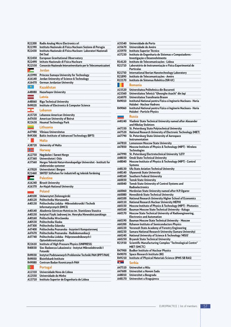
R22200 Radio Analog Micro Electronics srlR22390 Instituto Nazionale di Fisica Nucleare Sezione di PerugiaR22430 Instituto Nazionale di Fisica Nucleare Laboratori Nazionali
Del SudR22450 European Gravitational ObservatoryR22490 Istituto Nazionale di Fisica NucleareR22550 Consorzio Nazionale Interuniversitario per le Telecomunicazioni
JordanA15990 Princess Sumaya University for TechnologyA16140 Jordan University of Science & TechnologyA16470 German Jordanian University
KazakhstanA48080 Nazarbayev University
LatviaA48060 Riga Technical UniversityR49020 Institute of Electronics & Computer Science
LebanonA15720 Lebanese American UniversityA47650 American University of BeirutR22630 Houmal Technology Park
LithuaniaA47980 Vilniaus UniversitetasR49200 Baltic Institute of Advanced Technology (BPTI)
MaltaA38720 University of Malta
NorwayA12750 Høgskolen i Sørøst-NorgeA37360 Universitetet i OsloA37560 Norges Teknisk Naturvitenskapelige Universitet - Institutt for
elektroniske systemerA37820 Universitetet i BergenR21460 SINTEF Stiftelsen for industriell og teknisk forskning
PalestineA16240 Birzeit UniversityA16370 An-Najah National University
PolandA40100 Uniwersytet ZielonogórskiA40120 Politechnika WarszawskaA40130 Politechnika Lódzka - Mikroelektroniki I Technik
Informatycznych (DMCS)A40140 Akademia Górniczo-Hutnicza im. Stanislawa StaszicaA40150 Instytut Fizyki Jadrowej im. Henryka NiewodniczanskiegoA40160 Politechnika WroclawskaA40530 Politechnika SlaskaA47300 Politechnika GdanskaA47400 Politechnika Poznanska - Inzynierii KomputerowejA47670 Politechnika Poznanska - RadiokomunikacjiA47740 Politechnika Lódzka - Pólprzewodnikowych I
OptoelektronicznychR22610 Institute of High Pressure Physics (UNIPRESS)R40030 Siec Badawcza Lukasiewicz - Instytut Mikroelektroniki I
FotonikiR49030 Instytut Podstawowych Problemów Techniki PAN (IPPT-PAN)R49050 Bioinfobank InstituteR49080 Centrum Badan Kosmicznych PAN
PortugalA12310 Universidade Nova de LisboaA12550 Universidade do MinhoA13710 Instituto Superior de Engenharia de Lisboa
A35540 Universidade do PortoA35670 Universidade de AveiroA35970 Instituto Superior TécnicoA37230 Instituto de Engenharia de Sistemas e Computadores -
Investigação e DesenvolvimentoR14120 Instituto de Telecomunicações - LisboaR21710 Laboratório de Instrumentação e Física Experimental de
PartículasR21750 International Iberian Nanotechnology LaboratoryR21890 Instituto de Telecomunicações - AveiroR22170 Instituto de Sistemas Robótica (ISR-UC)
RomaniaA15520 Universitatea Politehnica din BucurestiA15560 Universitatea Tehnicã "Gheorghe Asachi" din IașșiA16070 Universitatea Transilvania BrasovR49010 Institutul National pentru Fizica si Inginerie Nucleara - Horia
Hulubei - Nuclear HadronsR49060 Institutul National pentru Fizica si Inginerie Nucleara - Horia
Hulubei - Particle Physics
RussiaA40240 Vladimir State Technical University named after Alexander
and Nikolay StoletovsA47330 St. Petersburg State Polytechnical UniversityA47520 National Research University of Electronic Technology (MIET)A47790 St. Petersburg State University of Aerospace
InstrumentationA47810 Lomonosov Moscow State UniversityA47850 Moscow Institute of Physics & Technology (MIPT) - Wireless
TechnologiesA47990 St. Petersburg Electrotechnical University 'LETI'A48030 Omsk State Technical UniversityA48040 Moscow Institute of Physics & Technology (MIPT) - Control
SystemsA48130 Ufa State Aviation Technical UniversityA48140 Ulyanovsk State UniversityA48160 Southern Federal UniversityA60030 Tomsk State UniversityA60040 Tomsk State University of Control Systems and
RadioelectronicsA60060 Mordovian State University named after N.P.OgarevA60080 Novosibirsk State Technical UniversityA60100 National Research University Higher School of EconomicsA60110 National Research Nuclear University MEPHIA60150 Moscow Institute of Physics & Technology (MIPT) - PhotonicsA60160 Bauman Moscow State Technical University - KalugaA60170 Moscow State Technical University of Radioengineering,
Electronics and AutomationA60190 Bauman Moscow State Technical University - MoscowA60200 Rzhanov Institute of Semiconductors PhysicsA60220 Voronezh State Academy of Forestry EngineeringA60230 Samara National Research University (Samara University)A60240 National University of Science & Technology 'MISiS'A60250 Bryansk State Technical UniversityR21930 Scientific Manufacturing Complex "Technological Centre"
MIET (SMCTC)R47900 Budker Institute of Nuclear PhysicsR49070 Space Research Institute (IKI)R49210 Institute of Physical Materials Science (IPMS SB RAS)
SerbiaA47510 Univerzitet u NišuA47600 Univerzitet u Novom SaduA48010 Univerzitet u BeograduA48170 Univerzitet u Kragujevcu
57EUROPRACTICE | list of members

SlovakiaA40050 Slovenská technická univerzita v BratislaveA47930 Technická univerzita v Kosiciach
SloveniaA40280 Univerza v LjubljaniA47690 Institut "Jozef Stefan"A47820 Univerza v MariboruR22580 Skylabs Vesoljske Tehnologije Doo
South AfricaA14560 University of Pretoria
SpainA12320 Universidad Politécnica de CartagenaA12590 Universidad de Castilla - La ManchaA13150 Universitat de ValènciaA13340 Universidad de AlcaláA13860 Universidad de SalamancaA14720 Universidad de La LagunaA15370 Universidad de DeustoA16290 Universitat Pompeu FabraA16340 University of Vigo - AtlanTTicA35130 Universidad Politécnica de Madrid - Departamento de
Ingeniería ElectrónicaA35190 Universitat Politècnica de ValènciaA35870 Universidad de Sevilla - Instituto de Microelectrónica de
Sevilla (IMSE-CNM)A35891 Universidad de CantabriaA36250 Universitat Autònoma de BarcelonaA36390 Universidad de Las Palmas de Gran Canaria - Instituto
Universitario de Microelectrónica Aplicada (IUMA)A37060 Universidad de Zaragoza - Dpto.Ingenieria Electronica y
ComunicacionesA37080 Universidad de Santiago de CompostelaA37330 Universidad Complutense de MadridA37580 Universidad de MalagaA37690 Universidad del Pais VascoA38330 Universidad de VigoA38360 Universitat de les Illes BalearsA38580 Universidad de Sevilla - Ingenieria ElectronicaA38590 Universidad de GranadaA38600 Universidad de NavarraA38660 Universitat de BarcelonaA38780 Universidad de Las Palmas de Gran Canaria - Departamento
de Informàtica y SistemasA38790 Universidad de Zaragoza - Facultad de CienciasA38820 Universidad Politécnica de Madrid - Centro de Electrónica
IndustrialA39080 Universidad de ExtremaduraA39100 Universidad Pública de NavarraA39150 Universitat Politècnica de Catalunya - Departamento de
Ingeniería Electrónica (Campus Nord)A39180 Universitat Rovira i VirgiliA39390 Universitat Autónoma de MadridA39540 Universidad Carlos III de MadridR00060 CNM - Instituto de Microelectrónica de BarcelonaR20700 IkerlanR20850 Centre Tecnològic de Telecomunicacions de CatalunyaR21230 Instituto de Fisica CorpuscularR21520 Institut de Ciències de L'EspaiR21550 Institut de Ciències FotòniquesR21740 Centro de Investigaciones Energéticas, Medioambientales y
TecnológicasR21910 Instituto de Tecnologías Físicas y de la InformaciónR22100 Centro Nacional de Supercomputación, BarcelonaR22460 Consorcio ESS Bilbao
R22470 Asociacion Centro TecnológicoR22600 Centro Tecnológico de Automoción de Galicia
SwedenA00260 Luleå tekniska universitetA13720 Uppsala universitetA16350 Stockholms universitetA16360 Kungliga Tekniska Hogskolan, StockholmA37350 Linköpings universitetA37370 Lunds universitetA38180 Kungliga Tekniska högskola, KistaA38670 Chalmers Tekniska högskolaA39840 MittuniversitetetR20690 Research Institutes of Sweden, ICT AcreoR20910 Totalförsvarets forskningsinstitut FOIR21700 MAX IV LaboratoryR21990 European Spallation SourceR22050 Institutet för Rymdfysik
SwitzerlandA05000 Scuola Universitaria Professionale della Svizzera ItalianaA12730 École Polytechnique Fédérale de Lausanne - Laboratoire de
Physique des Hautes EnergiesA12920 Universität ZürichA13090 Università della Svizzera ItalianaA13630 Université de GenèveA13780 Hochschule LuzernA14780 Haute école d'ingénierie et d'architecture FribourgA15480 Universität BaselA15530 Universität BernA16440 Universität ZurichA36110 École Polytechnique Fédérale de Lausanne - Microelectronics
SystemsA37340 École Polytechnique Fédérale de Lausanne - NeuchâtelA38100 Ostschweizer FachhochschuleA38310 Eidgenössische Technische Hochschule ZürichA38410 Berner FachhochschuleA38800 Eidgenössische Technische Hochschule Zürich - BaselA39760 Haute école du paysage d'ingénierie et d'architecture de
GenèveA39820 Fachhochschule NordwestschweizR20350 Organisation Européenne pour la Recherche NucléaireR20680 Centre Suisse d'Electronique et Microtechnique - NeuchâtelR20800 Paul Scherrer InstitutR20970 Centre Suisse d'Electronique et Microtechnique - ZürichR22180 Eidgenössische Materialprüfungs- und Forschungsanstalt
The NetherlandsA00170 Universiteit Twente - CAESA12010 Vrije Universiteit AmsterdamA12650 Radboud Universiteit NijmegenA13730 Stichting SaxionA14510 Rijksuniversiteit GroningenA15420 Erasmus Universitair Medisch Centrum RotterdamA15960 Universiteit van AmsterdamA35491 Universiteit Twente - Electrical EngineeringA35701 Technische Universiteit DelftA38050 Technische Universiteit EindhovenR00280 NikhefR20370 TNO-FELR20430 European Space Agency - ESTEC MicroelectronicsR20520 Stichting Nederlandse Wetenschappelijk Onderzoek
Instituten / Stichting ASTRON, Netherlands Institute for Radio Astronomy
R20540 European Space Agency - ESTEC Payload TechnologyR21200 Stichting imec NederlandR21250 NWO-I/SRON
58 EUROPRACTICE | list of members
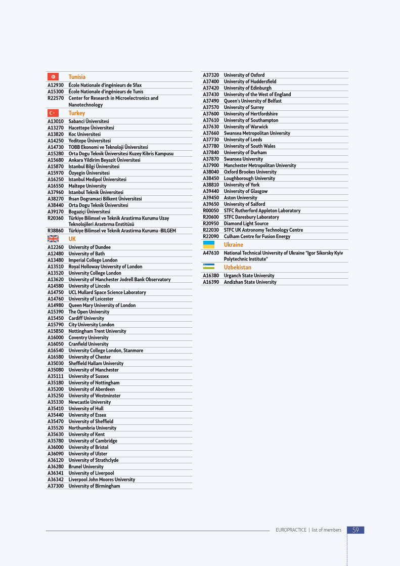
TunisiaA12930 École Nationale d'ingénieurs de SfaxA15300 École Nationale d'ingénieurs de TunisR22570 Center for Research in Microelectronics and
Nanotechnology
TurkeyA13010 Sabanci ÜniversitesiA13270 Hacettepe ÜniversitesiA13820 Koc UniversitesiA14250 Yeditepe ÜniversitesiA14730 TOBB Ekonomi ve Teknoloji ÜniversitesiA15280 Orta Dogu Teknik Üniversitesi Kuzey Kibris KampusuA15680 Ankara Yildirim Beyazit ÜniversitesiA15870 Istanbul Bilgi ÜniversitesiA15970 Özyegin ÜniversitesiA16250 Istanbul Medipol ÜniversitesiA16550 Maltepe UniversityA37960 Istanbul Teknik ÜniversitesiA38270 Ihsan Dogramaci Bilkent ÜniversitesiA38440 Orta Dogu Teknik ÜniversitesiA39170 Bogaziçi ÜniversitesiR20360 Türkiye Bilimsel ve Teknik Arastirma Kurumu Uzay
Teknolojileri Arastırma EnstitüsüR38860 Türkiye Bilimsel ve Teknik Arastirma Kurumu -BILGEM
UKA12260 University of DundeeA12480 University of BathA13480 Imperial College LondonA13510 Royal Holloway University of LondonA13520 University College LondonA13620 University of Manchester Jodrell Bank ObservatoryA14580 University of LincolnA14750 UCL Mullard Space Science LaboratoryA14760 University of LeicesterA14980 Queen Mary University of LondonA15390 The Open UniversityA15450 Cardiff UniversityA15790 City University LondonA15850 Nottingham Trent UniversityA16000 Coventry UniversityA16050 Cranfield UniversityA16540 University College London, StanmoreA16580 University of ChesterA35030 Sheffield Hallam UniversityA35080 University of ManchesterA35111 University of SussexA35180 University of NottinghamA35200 University of AberdeenA35250 University of WestminsterA35330 Newcastle UniversityA35410 University of HullA35440 University of EssexA35470 University of SheffieldA35520 Northumbria UniversityA35630 University of KentA35780 University of CambridgeA36000 University of BristolA36090 University of UlsterA36120 University of StrathclydeA36280 Brunel UniversityA36341 University of LiverpoolA36342 Liverpool John Moores UniversityA37300 University of Birmingham
A37320 University of OxfordA37400 University of HuddersfieldA37420 University of EdinburghA37430 University of the West of EnglandA37490 Queen's University of BelfastA37570 University of SurreyA37600 University of HertfordshireA37610 University of SouthamptonA37630 University of WarwickA37660 Swansea Metropolitan UniversityA37730 University of LeedsA37780 University of South WalesA37840 University of DurhamA37870 Swansea UniversityA37900 Manchester Metropolitan UniversityA38040 Oxford Brookes UniversityA38450 Loughborough UniversityA38810 University of YorkA39440 University of GlasgowA39450 Aston UniversityA39650 University of SalfordR00050 STFC Rutherford Appleton LaboratoryR20600 STFC Daresbury LaboratoryR20950 Diamond Light SourceR22030 STFC UK Astronomy Technology CentreR22090 Culham Centre for Fusion Energy
UkraineA47610 National Technical University of Ukraine "Igor Sikorsky Kyiv
Polytechnic Institute"
UzbekistanA16380 Urganch State UniversityA16390 Andizhan State University
59EUROPRACTICE | list of members

CONTACT INFORMATIONFor general information or enquiries about EUROPRACTICE, please contact the project coordination team at imec.
Romano Hoofman (general)Tel: +32 (0) 16 283865
Paul Malisse (operational)Tel: +32 (0) 16 281272E-mail: [email protected]
Wendy Fannes (legal)Tel: +32 (0) 16 281571E-mail: [email protected]
For enquiries about EUROPRACTICE academic membership, design tools or training courses, please contact the Microelectronics Support Centre, STFC Rutherford Appleton Laboratory, on:
Mark Willoughby (design tools)Tel: +44 (0) 1235 445327E-Mail: [email protected]
Clive Holmes (training courses)Tel: +44 (0) 1235 445327E-Mail: [email protected]
Richard Bishop (academic membership)Tel: +44 (0) 1235 445327E-Mail: [email protected]
For enquiries about EUROPRACTICE smart system integration, please contact Smart Systems Integration service center:
Ramsey Selim (general)Tel: +353 21 234 6613E-mail: [email protected]
For more specific enquiries concerning technology access, MPW schedules, and related customer support, please contact one of the following EUROPRACTICE support centers.
ON Semiconductor:Greta Milczanowska Tel: +32 (0) 16 281274E-mail: [email protected]
TSMC TechnologiesTobias VanderhenstTel: +32 (0)16 287889E-mail: [email protected]
UMC TechnologiesErwin Deumens Tel: +32 (0)16 281930E-mail: [email protected]
X-FAB & MEMS TechnologiesPieter ClaesTel: +32 (0)16 288770E-mail: [email protected]
Si-Photonics TechnologiesMateo Aranda MoranTel: +32 (0)16 283045E-mail: [email protected]
SiN-Photonics TechnologiesAdil MasoodTel: +32 (0)16 288054E-mail: [email protected]
ams TechnologiesElvira LiandresTel: +49 (0)9131 776-4464E-mail: [email protected]
GLOBALFOUNDRIES TechnologiesVikas Vijaya KumarTel: +49 (0)9131 776-4418E-mail: [email protected]
IHP TechnologiesElvira LiandresTel: +49 (0)9131 776-4464E-mail: [email protected]
X-FAB TechnologiesStefan RudischhauserTel: +49 (0)9131 776-4422 E-mail: [email protected]
GaN-IC TechnologyMaritza Tangarife OrtizTel: +32 (0)16 281372E-mail: [email protected]
ams TechnologiesKholdoun TorkiTel: +33-476 574615E-mail: [email protected]
EM Microelectronic TechnologiesNicolas Partenza Tel: +33-476 528919 E-mail: [email protected]
ON Semiconductor TechnologiesFrançois BertholletTel: +33-476 574621E-mail: [email protected]
STMicroelectronics TechnologiesJean-Francois PaillotinTel: +33-476 574797E-mail: [email protected]
MEMS TechnologiesKholdoun TorkiTel: +33-476 574615E-mail: [email protected]
Si-Photonics TechnologiesFrançois BertholletTel: +33-476 574621E-mail: [email protected]
60 EUROPRACTICE | contact information

The EUROPRACTICE Service has received funding from the European Union through
the H2020 framework program for research, technological development and
demonstration under grant agreementN° 825121.
This funding is exclusively used to support European SMEs, universities and
research laboratories.© IT
ESO,
Jesu
it Un
iver
sity o
f Gua
dala
jara
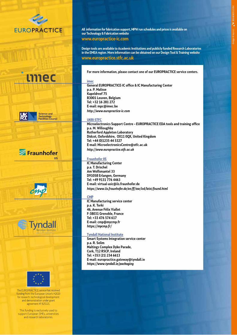
The EUROPRACTICE service has received funding from the European Union’s H2020 for research, technological development
and demonstration under grant agreement N° 825121.
This funding is exclusively used to
support European SMEs, universities and research laboratories.
desig
n &
layo
ut:All information for fabrication support, MPW run schedules and prices is available on
our Technology & Fabrication website
www.europractice-ic.com
For more information, please contact one of our EUROPRACTICE service centers.
imecGeneral EUROPRACTICE-IC office & IC Manufacturing Centerp.a. P. MalisseKapeldreef 75B3001 Leuven, BelgiumTel: +32 16 281 272E-mail: [email protected]://www.europractice-ic.com UKRI-STFCMicroelectronics Support Centre – EUROPRACTICE EDA tools and training officep.a. M. WilloughbyRutherford Appleton LaboratoryDidcot, Oxfordshire, OX11 0QX, United KingdomTel: +44 (0)1235 44 5327E-mail: [email protected]://www.europractice.stfc.ac.uk
Fraunhofer IIS IC Manufacturing Centerp.a. T. DrischelAm Wolfsmantel 33D91058 Erlangen, GermanyTel: +49 9131 776 4463E-mail: [email protected]://www.iis.fraunhofer.de/en/ff/sse/icd/leist/found.html
CMPIC Manufacturing service centerp.a. K. Torki46, Avenue Félix VialletF-38031 Grenoble, FranceTel: +33 476 574 617E-mail: [email protected]://mycmp.fr/
Tyndall National InstituteSmart Systems Integration service centerp.a. R. SelimMaltings Complex Dyke Parade, Cork, T12 R5CP, IrelandTel: +353 (21) 234 6613E-mail: [email protected]://www.tyndall.ie/packaging
Design tools are available to Academic Institutions and publicly funded Research Laboratories in the EMEA region. More information can be obtained on our Design Tool & Training website
www.europractice.stfc.ac.uk