The 2017 IRDS Lithography Roadmap
23
The 2017 IRDS Lithography Roadmap International Workshop on Advanced Patterning Solutions Mark Neisser Kempur Microelectronic Materials October, 2018
Transcript of The 2017 IRDS Lithography Roadmap

The 2017 IRDS Lithography
Roadmap
International Workshop on Advanced
Patterning Solutions
Mark Neisser
Kempur Microelectronic Materials
October, 2018
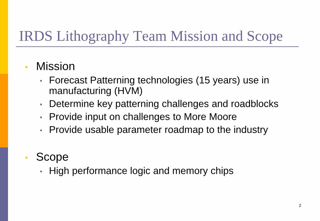
IRDS Lithography Team Mission and Scope
• Mission• Forecast Patterning technologies (15 years) use in
manufacturing (HVM)
• Determine key patterning challenges and roadblocks
• Provide input on challenges to More Moore
• Provide usable parameter roadmap to the industry
• Scope• High performance logic and memory chips
2
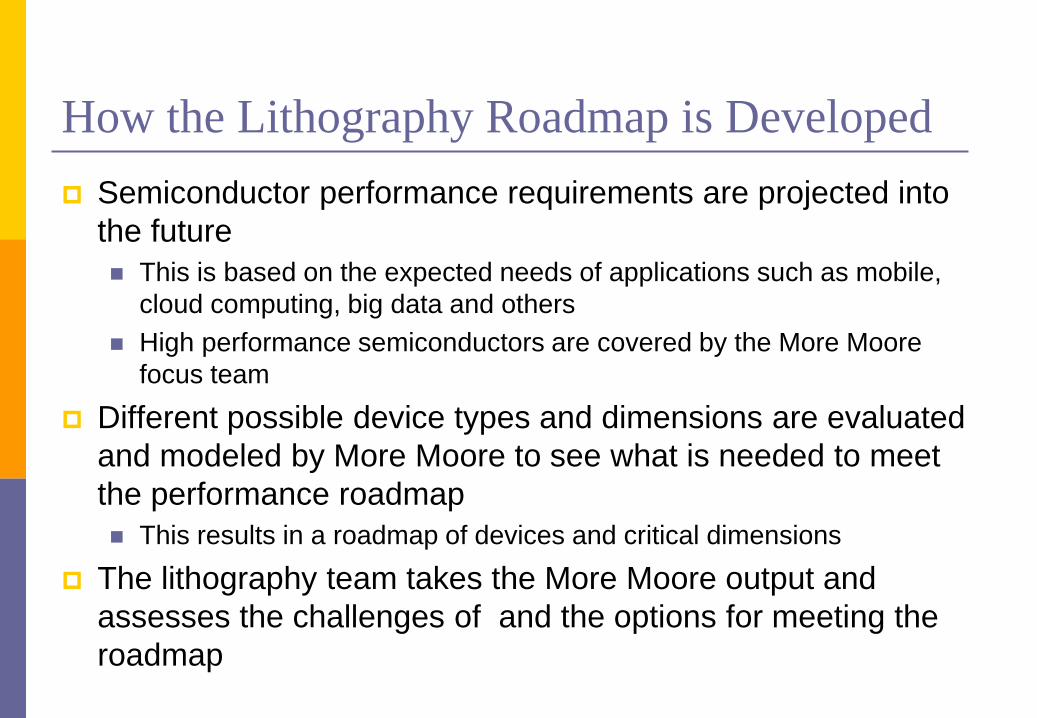
How the Lithography Roadmap is Developed
Semiconductor performance requirements are projected into
the future
◼ This is based on the expected needs of applications such as mobile,
cloud computing, big data and others
◼ High performance semiconductors are covered by the More Moore
focus team
Different possible device types and dimensions are evaluated
and modeled by More Moore to see what is needed to meet
the performance roadmap
◼ This results in a roadmap of devices and critical dimensions
The lithography team takes the More Moore output and
assesses the challenges of and the options for meeting the
roadmap
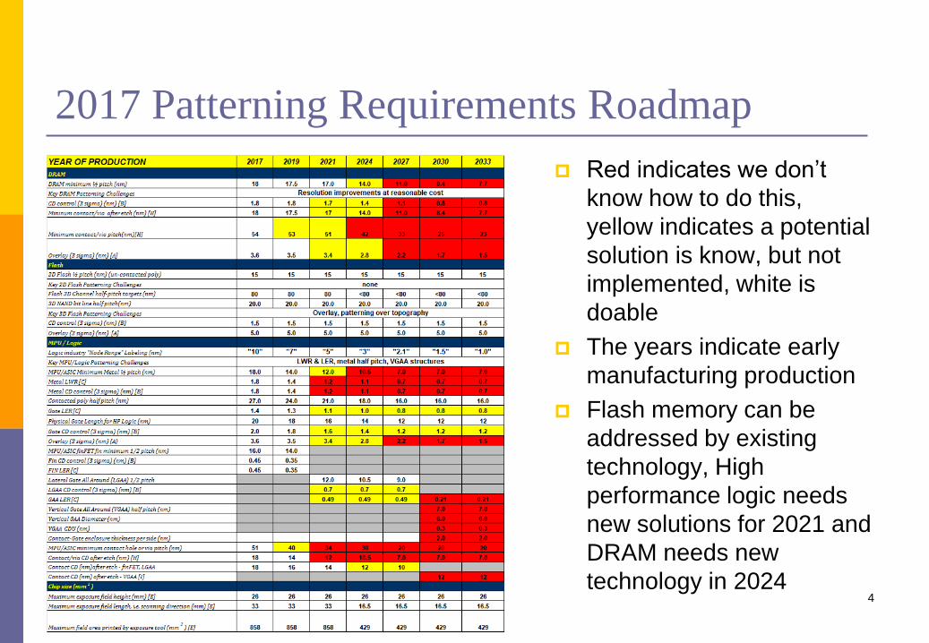
2017 Patterning Requirements Roadmap
Red indicates we don’t
know how to do this,
yellow indicates a potential
solution is know, but not
implemented, white is
doable
The years indicate early
manufacturing production
Flash memory can be
addressed by existing
technology, High
performance logic needs
new solutions for 2021 and
DRAM needs new
technology in 20244
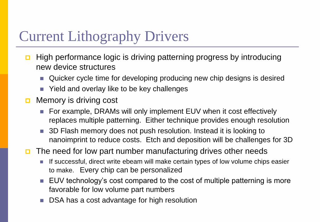
Current Lithography Drivers
High performance logic is driving patterning progress by introducing
new device structures
◼ Quicker cycle time for developing producing new chip designs is desired
◼ Yield and overlay like to be key challenges
Memory is driving cost
◼ For example, DRAMs will only implement EUV when it cost effectively
replaces multiple patterning. Either technique provides enough resolution
◼ 3D Flash memory does not push resolution. Instead it is looking to
nanoimprint to reduce costs. Etch and deposition will be challenges for 3D
The need for low part number manufacturing drives other needs
◼ If successful, direct write ebeam will make certain types of low volume chips easier
to make. Every chip can be personalized
◼ EUV technology’s cost compared to the cost of multiple patterning is more
favorable for low volume part numbers
◼ DSA has a cost advantage for high resolution
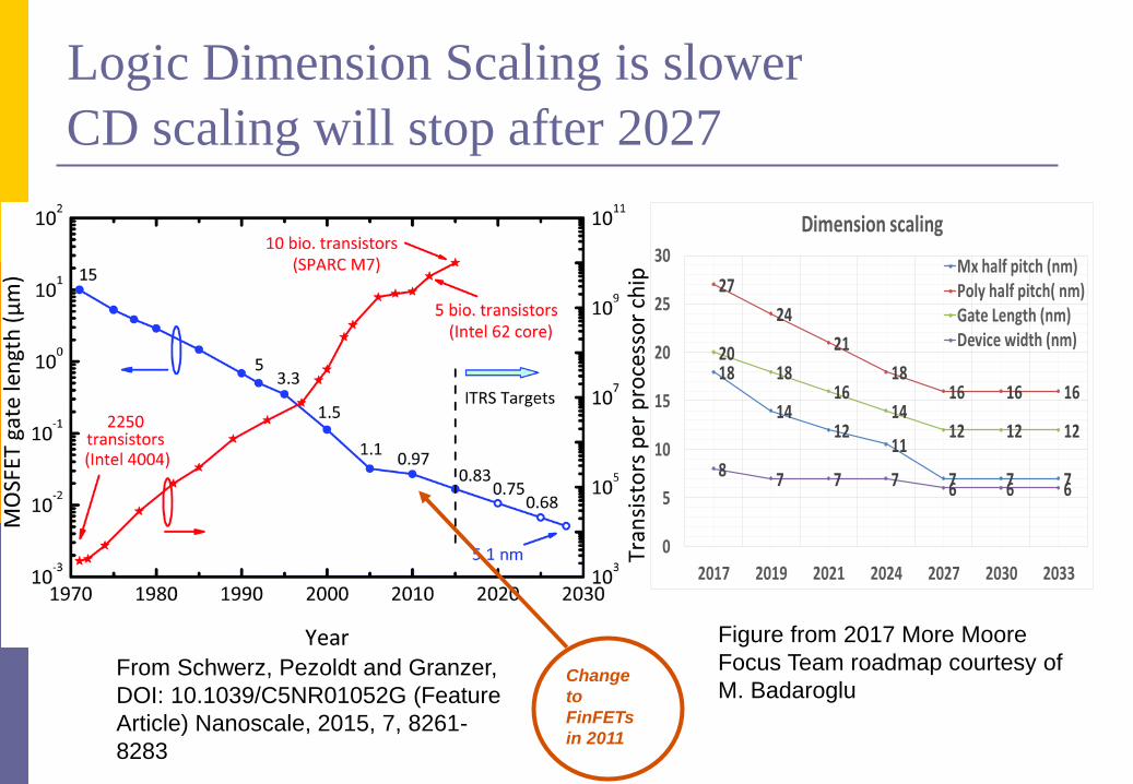
Logic Dimension Scaling is slower
18
1412
11
7 7 7
27
24
21
1816 16 16
2018
1614
12 12 12
8 7 7 7 6 6 6
0
5
10
15
20
25
30
2017 2019 2021 2024 2027 2030 2033
Dimension scaling
Mx half pitch (nm)Poly half pitch( nm)Gate Length (nm)Device width (nm)
Figure from 2017 More Moore
Focus Team roadmap courtesy of
M. BadarogluFrom Schwerz, Pezoldt and Granzer,
DOI: 10.1039/C5NR01052G (Feature
Article) Nanoscale, 2015, 7, 8261-
8283
Change
to
FinFETs
in 2011
CD scaling will stop after 2027
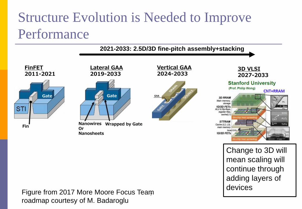
Structure Evolution is Needed to Improve
Performance
7
Lateral GAA2019-2033
FinNanowiresOrNanosheets
Wrapped by Gate
FinFET2011-2021
Vertical GAA2024-2033
3D VLSI2027-2033
Gate Gate
2021-2033: 2.5D/3D fine-pitch assembly+stacking
Figure from 2017 More Moore Focus Team
roadmap courtesy of M. Badaroglu
Change to 3D will
mean scaling will
continue through
adding layers of
devices
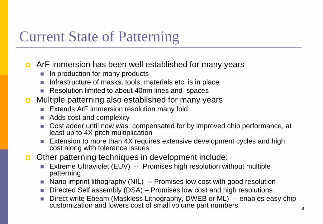
Current State of Patterning
ArF immersion has been well established for many years◼ In production for many products
◼ Infrastructure of masks, tools, materials etc. is in place
◼ Resolution limited to about 40nm lines and spaces
Multiple patterning also established for many years◼ Extends ArF immersion resolution many fold
◼ Adds cost and complexity
◼ Cost adder until now was compensated for by improved chip performance, at least up to 4X pitch multiplication
◼ Extension to more than 4X requires extensive development cycles and high cost along with tolerance issues
Other patterning techniques in development include:◼ Extreme Ultraviolet (EUV) -- Promises high resolution without multiple
patterning
◼ Nano imprint lithography (NIL) -- Promises low cost with good resolution
◼ Directed Self assembly (DSA) – Promises low cost and high resolutions
◼ Direct write Ebeam (Maskless Lithography, DWEB or ML) -- enables easy chip customization and lowers cost of small volume part numbers
8
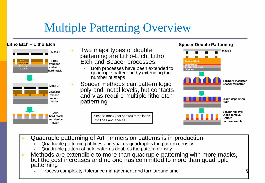
Multiple Patterning Overview
▪ Two major types of double patterning are Litho-Etch, Litho Etch and Spacer processes. ▪ Both processes have been extended to
quadruple patterning by extending the number of steps
▪ Spacer methods can pattern logic poly and metal levels, but contacts and vias require multiple litho etch patterning
9
Mask 1
Mask 2
trenches
and etch
hard mask
Coat and
expose
second
resist
Etch
hard mask
and device
layer
Litho Etch – Litho Etch
Resist
Substrate
Device layer
Hard mask
Spacer Double Patterning
Top Hard Mask Top Hard Mask
Bottom Hard Mask Bottom Hard Mask Buffer Oxide Buffer Oxide
SubstrateSubstrate
Mask 1
Top hard masketchSpacer formation
Oxide depositionCMP
Spacer removalOxide removalBottom hard masketch
Second mask (not shown) trims loops
into lines and spaces.
▪ Quadruple patterning of ArF immersion patterns is in production▪ Quadruple patterning of lines and spaces quadruples the pattern density▪ Quadruple pattern of hole patterns doubles the pattern density
▪ Methods are extendible to more than quadruple patterning with more masks, but the cost increases and no one has committed to more than quadruple patterning▪ Process complexity, tolerance management and turn around time
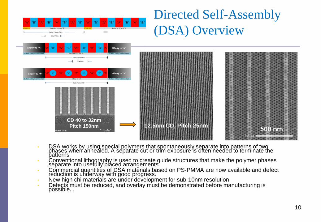
Directed Self-Assembly
(DSA) Overview
• DSA works by using special polymers that spontaneously separate into patterns of two phases when annealed. A separate cut or trim exposure is often needed to terminate the patterns
• Conventional lithography is used to create guide structures that make the polymer phases separate into usefully placed arrangements
• Commercial quantities of DSA materials based on PS-PMMA are now available and defect reduction is underway with good progress.
• New high chi materials are under development for sub-10nm resolution• Defects must be reduced, and overlay must be demonstrated before manufacturing is
possible. .
10
12.5nm CD, Pitch 25nmCD 40 to 32nm
Pitch 150nm
Affinity to "A"
Guide Pattern Pitch
Guide Pattern CD
Guide Pattern CD
Surface Affinity is UnimportantAffinity for "A"
Neutral to "A" and "B" Surface Affinity is Unimportant
Final Pitch
"A""A" "B""B"
"A""A" "A"
"A"
Surface Affinity is Unimportant
"A" "B"
"A" "A"
Surface Affinity is Unimportant
"B"
Final Pitch
"A"
Neutral to "A" and "B" Affinity to "A" Neutral to "A" and "B"
"B""B" "A" "B" "A" "B" "A""A" "B" "A" "B" "A""A" "B" "A" "B"
"B""B""B""B"Affinity to "A"
Affinity to "A" Affinity to "A"
Affinity to "A"
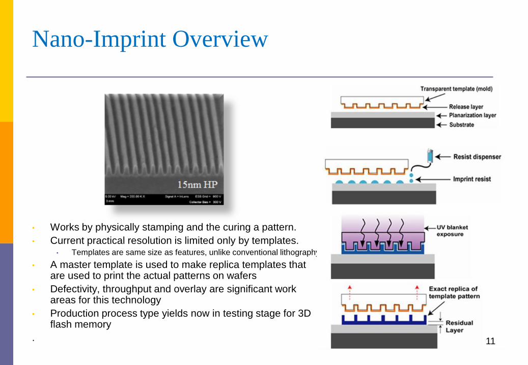
Nano-Imprint Overview
• Works by physically stamping and the curing a pattern.
• Current practical resolution is limited only by templates.• Templates are same size as features, unlike conventional lithography
• A master template is used to make replica templates that are used to print the actual patterns on wafers
• Defectivity, throughput and overlay are significant work areas for this technology
• Production process type yields now in testing stage for 3D flash memory
. 11
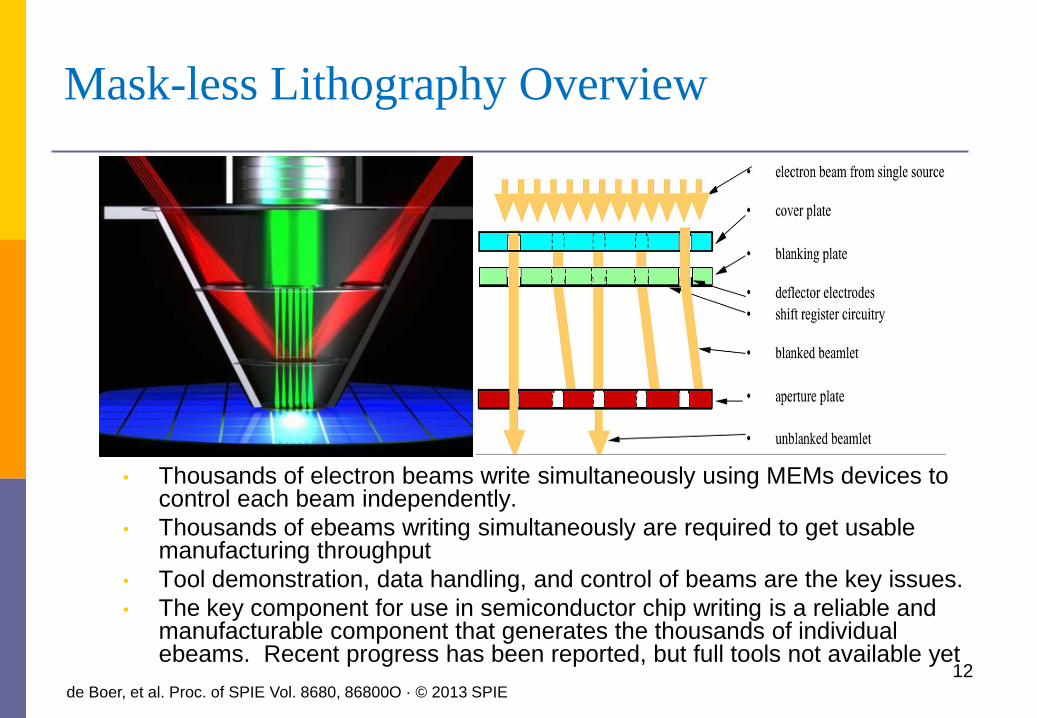
Mask-less Lithography Overview
• Thousands of electron beams write simultaneously using MEMs devices to control each beam independently.
• Thousands of ebeams writing simultaneously are required to get usable manufacturing throughput
• Tool demonstration, data handling, and control of beams are the key issues.
• The key component for use in semiconductor chip writing is a reliable and manufacturable component that generates the thousands of individual ebeams. Recent progress has been reported, but full tools not available yet
12de Boer, et al. Proc. of SPIE Vol. 8680, 86800O · © 2013 SPIE
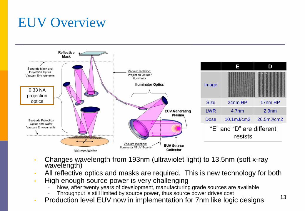
EUV Overview
• Changes wavelength from 193nm (ultraviolet light) to 13.5nm (soft x-ray wavelength)
• All reflective optics and masks are required. This is new technology for both• High enough source power is very challenging
• Now, after twenty years of development, manufacturing grade sources are available• Throughput is still limited by source power, thus source power drives cost
• Production level EUV now in implementation for 7nm like logic designs13
E D
Image
Size 24nm HP 17nm HP
LWR 4.7nm 2.9nm
Dose 10.1mJ/cm2 26.5mJ/cm2
0.33 NA
projection
optics
“E” and “D” are different
resists
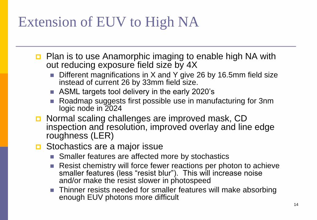
Extension of EUV to High NA
Plan is to use Anamorphic imaging to enable high NA with out reducing exposure field size by 4X◼ Different magnifications in X and Y give 26 by 16.5mm field size
instead of current 26 by 33mm field size.
◼ ASML targets tool delivery in the early 2020’s
◼ Roadmap suggests first possible use in manufacturing for 3nm logic node in 2024
Normal scaling challenges are improved mask, CD inspection and resolution, improved overlay and line edge roughness (LER)
Stochastics are a major issue◼ Smaller features are affected more by stochastics
◼ Resist chemistry will force fewer reactions per photon to achieve smaller features (less “resist blur”). This will increase noise and/or make the resist slower in photospeed
◼ Thinner resists needed for smaller features will make absorbing enough EUV photons more difficult
14
Stochastics
Stochastics, not resolution, limit useful resolution of EUV
◼ The k1 values achieved for EUV printing are much higher than
those for ArF
◼ Stochastics affect LER, LWR and CDU
Stochastics cause missing contact hole, line bridging and
line cuts
◼ The frequency of these defects is worse than predicted from simple
extrapolation using mean and sigma for CD
◼ There is a bad tail on actual distributions
◼ This tail has been observed experimentally and predicted by
simulation
The limiting factor for EUV application and extension is the
industry’s ability to deal with this noise factor
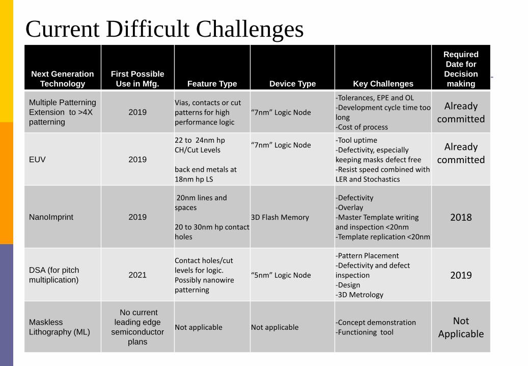
Current Difficult Challenges
Next Generation
Technology
First Possible
Use in Mfg. Feature Type Device Type Key Challenges
Required
Date for
Decision
making
Multiple Patterning
Extension to >4X
patterning
2019
Vias, contacts or cut patterns for high performance logic
“7nm” Logic Node
-Tolerances, EPE and OL-Development cycle time too long-Cost of process
Already committed
EUV 2019
22 to 24nm hpCH/Cut Levels
back end metals at 18nm hp LS
“7nm” Logic Node-Tool uptime-Defectivity, especially keeping masks defect free-Resist speed combined with LER and Stochastics
Already committed
NanoImprint 2019
20nm lines and spaces
20 to 30nm hp contact holes
3D Flash Memory
-Defectivity-Overlay-Master Template writing and inspection <20nm-Template replication <20nm
2018
DSA (for pitch
multiplication)2021
Contact holes/cut levels for logic. Possibly nanowire patterning
“5nm” Logic Node
-Pattern Placement-Defectivity and defect inspection-Design -3D Metrology
2019
Maskless
Lithography (ML)
No current
leading edge
semiconductor
plans
Not applicable Not applicable-Concept demonstration-Functioning tool
Not Applicable
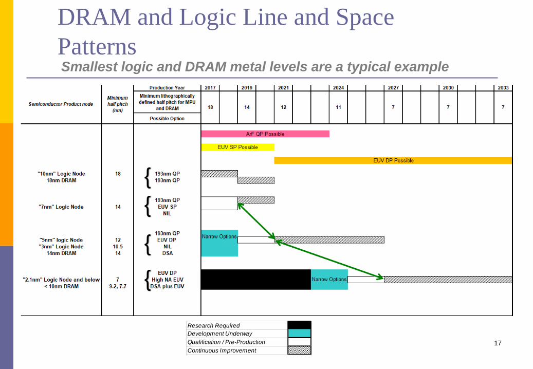
DRAM and Logic Line and Space
Patterns
17
Smallest logic and DRAM metal levels are a typical example
Research Required
Development Underway
Qualification / Pre-Production
Continuous Improvement
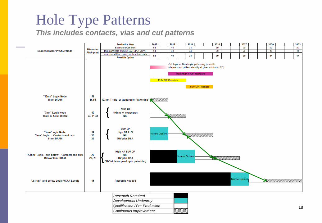
Hole Type Patterns
18
This includes contacts, vias and cut patterns
Research Required
Development Underway
Qualification / Pre-Production
Continuous Improvement
VGAA Projected Structure
• The green area underneath the drain (D) is the actual gate silicon surround by some thin gate insulator
• The gate contact is to the x-side of the drain and the source contact is to the y-side of the drain.
• The pitch from gate to drain or source is 14nm
• The gate silicon is 6nm in diameter
• The gate plus gate insulator diameter is 10nm in diameter
19
Gate x-pitch
S G S
DG
Drain pick-upfrom top
Gate pick-upfrom side
2D device (finFET)3D device (vertical GAA)
2D SoC/bottom tier
S
DG D
24nm x-pitch
S
Gate x-pitch
DGGate
y-pitch
24nm y-pitch
3D deviceHigher tiers
DG D
24nm x-pitch
S
13nm y-pitch
Source pick-upfrom bottom
Gate x-pitch
S
DD
Fin pitch
LgateLgate
Layout view Layout view
Cross-section view
Layout view
Cross-section view
Gatey-pitch
Lithography Difficult Challenges – Near Term 2018-2023
• Stochastics• Random variations in light intensity combined with random variation in the exact
position of molecules in a photoresist film already create significant pattern variation. They also create defects. This will be a bigger issue as feature sizes shrink
• Defectivity• Every possible new patterning method for improved resolution needs improved
defectivity at some part or parts of the process
• Inspection and Metrology• Smaller features and thinner films, along with tighter desired tolerances will drive
new inspection methods and metrology.
• Etch and metrology of 3D structures will be challenging
• Overlay and edge placement error (EPE)• These affect both product reliability and performance. Improvement is always
needed and leading edge resolution is always at the current limit of overlay and EPE capability.
• Patterning of small hole type patterns, particularly VGAA• VGAA performance is needed to continue enough chip performance progress
• Some combination of high resolution patterning, process defined dimensions and self-aligned features will probably be needed
20
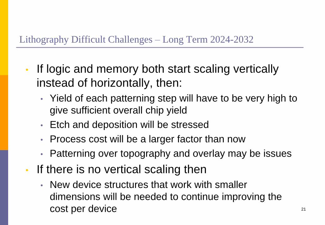
Lithography Difficult Challenges – Long Term 2024-2032
• If logic and memory both start scaling vertically
instead of horizontally, then:
• Yield of each patterning step will have to be very high to
give sufficient overall chip yield
• Etch and deposition will be stressed
• Process cost will be a larger factor than now
• Patterning over topography and overlay may be issues
• If there is no vertical scaling then
• New device structures that work with smaller
dimensions will be needed to continue improving the
cost per device 21
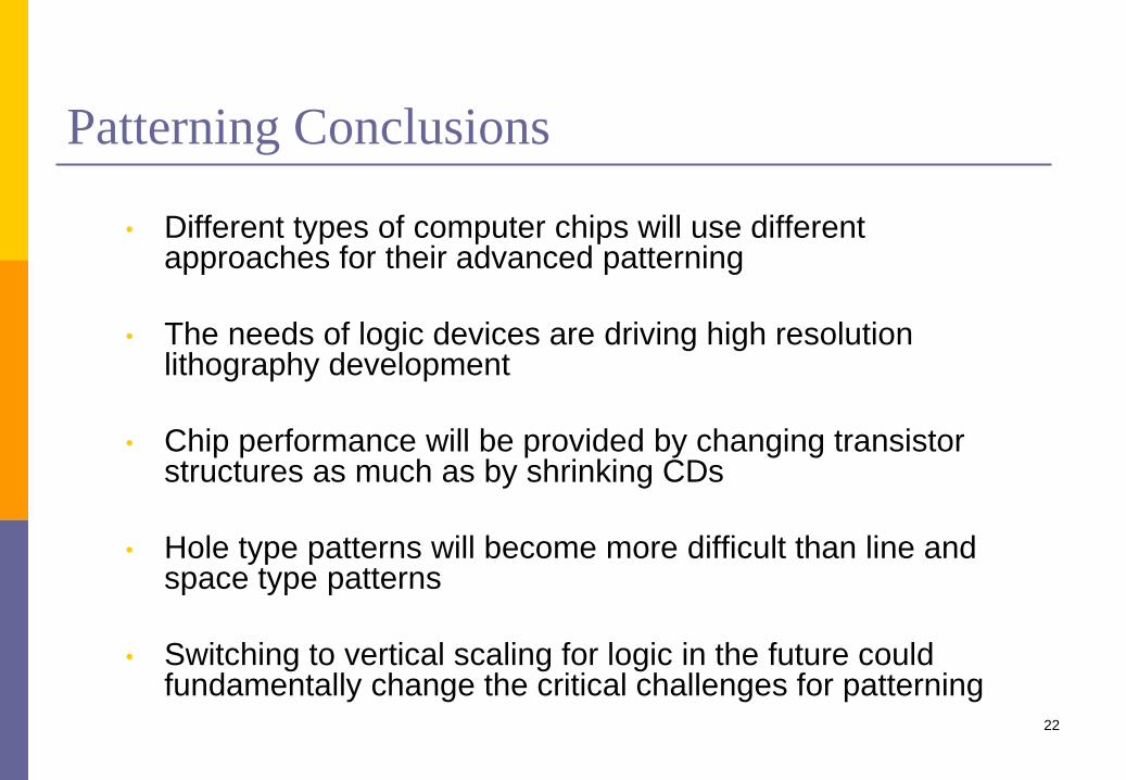
• Different types of computer chips will use different approaches for their advanced patterning
• The needs of logic devices are driving high resolution lithography development
• Chip performance will be provided by changing transistor structures as much as by shrinking CDs
• Hole type patterns will become more difficult than line and space type patterns
• Switching to vertical scaling for logic in the future could fundamentally change the critical challenges for patterning
22
Patterning Conclusions
谢 谢!Thanks for your attention.