Music PC Set-Up with a 192KHz/24Bit asynchronous USB Audio Device
1. General Description
2. Features
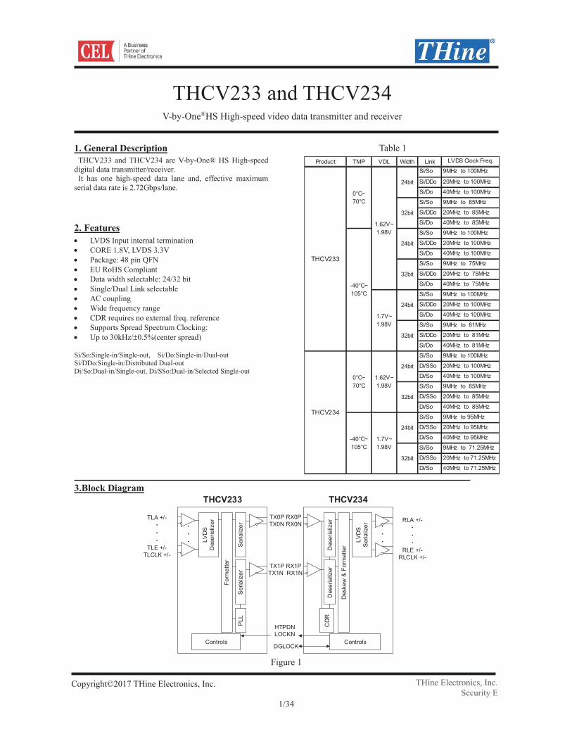
3.Block Diagram
Product VDL Width Link LVDS Clock Freq.
Si/So 9MHz to 100MHz
Si/DDo 20MHz to 100MHz
Si/Do 40MHz to 100MHz
Si/So 9MHz to 85MHz
Si/DDo 20MHz to 85MHz
Si/Do 40MHz to 85MHz
Si/So 9MHz to 100MHz
Si/DDo 20MHz to 100MHz
Si/Do 40MHz to 100MHz
Si/So 9MHz to 75MHz
Si/DDo 20MHz to 75MHz
Si/Do 40MHz to 75MHz
Si/So 9MHz to 100MHz
Si/DDo 20MHz to 100MHz
Si/Do 40MHz to 100MHz
Si/So 9MHz to 81MHz
Si/DDo 20MHz to 81MHz
Si/Do 40MHz to 81MHz
Si/So 9MHz to 100MHz
Di/SSo 20MHz to 100MHz
Di/So 40MHz to 100MHz
Si/So 9MHz to 85MHz
Di/SSo 20MHz to 85MHz
Di/So 40MHz to 85MHz
Si/So 9MHz to 95MHz
Di/SSo 20MHz to 95MHz
Di/So 40MHz to 95MHz
Si/So 9MHz to 71.25MHz
Di/SSo 20MHz to 71.25MHz
Di/So 40MHz to 71.25MHz
THCV234
0°C~70°C
1.62V~1.98V
24bit
32bit
-40°C~105°C
1.7V~1.98V
24bit
32bit
THCV233
0°C~70°C
1.62V~1.98V
24bit
32bit
-40°C~105°C
24bit
32bit
1.7V~1.98V
24bit
32bit
TLA +/-
TLE +/-TLCLK +/-
LVD
SD
eser
ializ
er
Form
atte
r
Ser
ializ
erS
eria
lizer
PLL
Controls
Des
eria
lizer
Des
eria
lizer
CD
R
Des
kew
&Fo
rmat
ter
LVD
SS
eria
lizer
THCV233 THCV234
RLA +/-
RLE +/-RLCLK +/-
Controls
TX0P RX0PTX0N RX0N
TX1P RX1PTX1N RX1N
HTPDNLOCKN
DGLOCK

Contents Page
1. General Description............................................................................................................................................. 1 2. Features ................................................................................................................................................................ 1 3.Block Diagram ...................................................................................................................................................... 1 4. Pin Configuration ................................................................................................................................................ 4 5. Pin Description..................................................................................................................................................... 5 6. Operation Mode................................................................................................................................................... 7 7. Function Description ........................................................................................................................................... 8
8. Absolute Maximum Ratings.............................................................................................................................. 19 9. Operating Conditions ........................................................................................................................................ 20 10. Electrical Specifications .................................................................................................................................. 21
11. AC Timing Diagrams and Test Circuits ......................................................................................................... 26

Package................................................................................................................................................................... 33 Notices and Requests ............................................................................................................................................. 34

4. Pin Configuration
LAV
DH
LAG
ND
Res
erve
d[8]
Res
erve
d[7]
MO
DE
[1]
MO
DE
[0]
VD
DP
RE
Res
erve
d[6]
BE
TR
eser
ved[
5]P
DN
36 35 34 33 32 31 30 29 28 27 26 25TLA- 37 24 HTPDN
TLA+ 38 23 LOCKNTLB- 39 22 CAVDL
TLB+ 40 21 CAGNDTLC- 41 20 TX0N
TLC+ 42 19 TX0PTLCLK- 43 18 CAGND
TLCLK+ 44 17 TX1NTLD- 45 16 TX1P
TLD+ 46 15 CAGNDTLE- 47 14 CAVDL
TLE+ 48 13 CPVDL1 2 3 4 5 6 7 8 9 10 11 12LA
VD
HLA
GN
DC
OL
DE
INR
eserved[0]V
SS
VD
DR
eserved[1]D
ES
EL
Reserved[2]
Reserved[3]
Reserved[4]
THCV233QFN-48pin
Exposed PAD
(TOP VIEW)49 EXPGND
DG
LOC
KP
DN
Res
erve
d[9]
Res
erve
d[8]
RS
VD
DM
OD
E[0
]M
OD
E[1
]R
eser
ved[
7]R
eser
ved[
6]LA
GN
DLA
VD
H
36 35 34 33 32 31 30 29 28 27 26 25HTPDN 37 24 RLA-LOCKN 38 23 RLA+CAGND 39 22 RLB-
RX0N 40 21 RLB+RX0P 41 20 RLC-
CAVDL 42 19 RLC+CAGND 43 18 RLCLK-
RX1N 44 17 RLCLK+RX1P 45 16 RLD-
CAGND 46 15 RLD+CAVDL 47 14 RLE-
BET 48 13 RLE+1 2 3 4 5 6 7 8 9 10 11 12R
eserved[0]R
eserved[1]R
eserved[2]R
eserved[3]R
eserved[4]V
DD
VS
SR
eserved[5]D
EO
UT
CO
LLA
GN
DLA
VD
H
THCV234QFN-48pin
Exposed PAD
(TOP VIEW)49 EXPGND
5. Pin Description
Pin Name Pin # Type* DescriptionTLA -/+ 37,38 LITLB -/+ 39,40 LITLC -/+ 41,42 LITLCLK -/+ 43,44 LITLD -/+ 45,46 LITLE -/+ 47,48 LITX0N/P 20,19 COTX1N/P 17,16 CO
LOCKN 23 I Lock detect input(LOCKN).It must be connected to Rx LOCKN with a Tx side 10kΩ pull-up resistor. LOCKN is input only.
HTPDN 24 I Hot plug detect input (HTPDN).It must be connected to Rx HTPDN with a Tx side 10kΩ pull-up resistor. HTPDN is input only.
Reserved [3,2,0] 11,10,5 - It must be open.
Reserved [1] 8 - It must be connected with a pull-up resistor to 3.3V.
DEIN 4 I
DE input for LVDS data sets (DEIN).DEIN is external DE input pin. When input LVDS does not contain DE signal, DE can be provided as external input.Activation of DEIN function follow the following settings. DESEL=L : DE input from DEIN is used for processing. DESEL=H : DE input from LVDS is used for processing.
DESEL 9 IDE input selector. H : DE input from LVDS is used for processing L : DE input from DEIN is used for processing
Reserved[4,5,6,7,8]
12,26,2833,34 I It must be connected to GND.
MODE [1:0] 32,31 I
Operation mode select input.MODE[1:0] =LL : Single-in/Distribution dual-out =LH : Single-in/Single-out =HL : Single-in/Dual-out =HH : Reserved (Forbidden)
PDN 25 I Power down Schmitt input. H: Normal operation, L: Power down
PRE 29 I Pre-Emphasis level select input for High Speed CML signal output. H : 100%, L : 0%
COL 3 I Data width setting for High speed CML signal output. H : 24bit, L : 32bit
BET 27 I Field-BET entry. H : Field BET Operation, L : Normal Operation
LAVDH 1,36 P33 LVDS power supply (3.3V)LAGND 2,35 GND LVDS GNDCAVDL 22,14 P18 High-speed signal analog power supply (1.8V)CAGND 21,18,15 GND High-speed signal analog GNDCPVDL 13 P18 High-speed signal PLL power supply (1.8V)VDD 7,30 P18 Logic power supply (1.8V)VSS 6 GND Logic GNDEXPGND 49 GND EXPOSED PAD GND
LVDS signal input.
High-speed CML signal output.
Pin Name Pin # Type* DescriptionRLA -/+ 24,23 LORLB -/+ 22,21 LORLC -/+ 20,19 LORLCLK -/+ 18,17 LORLD -/+ 16,15 LORLE -/+ 14,13 LORX0N/P 40,41 CIRX1N/P 44,45 CI
LOCKN 38 OD Lock detect output (LOCKN).It must be connected to Tx LOCKN with a Tx side10kΩ pull-up resistor. LOCKN is output only.
HTPDN 37 OD Hot plug detect output (HTPDN).It must be connected to Tx HTPDN with a Tx side 10kΩ pull-up resistor. HTPDN is output only.
Reserved [1,2] 2,3 - It must be open.
Reserved [5] 8 - It must be connected with a pull-up resistor to 3.3V.
DEOUT 9 O
DE signal output (DEOUT) for LVDS data sets.When used as DEOUT, no external component is required. It is push pull output.DEOUT output DE timing depending upon data stream state. DEOUT is output only.
Bit Error Test (BET) result output under Field-BET operation H : No error, L : Bit error occured
DGLOCK 36 BPUMultiple-chip configuration total Rx side LOCKN indicator (DGLOCK).When used as DGLOCK, it is internally connected with a pull-up resistor to 3.3V. No external component is required.LOCKN arrange among Rx Multiple-chip configuration is achieved by connecting all DGLOCK pins.
Reserved[0,3,4,6,7,8,9]
1,4,5,27,28,33,34 - It must be connected to GND.
MODE [1:0] 29,30 I
Operation mode select input.MODE [1:0] =LL : Dual-in/Selected single-out (Lane0) =LH : Dual-in/Single-out =HL : Dual-in/Selected single-out (Lane1) =HH : Single-in/Single-out
PDN 35 I Power down Schmitt input. H: Normal operation, L: Power down
RS 32 I
LVDS output swing range select input. H : Normal swing (350mv@typ.), L : Reduced swing (200mv@typ.)Latch select input under Field-BET operation H : Latched result, L : NOT Latched result
COL 10 I Data width setting for High Speed CML signal output. H : 24bit, L : 32bit
BET 48 I Field-BET entry. H : Field BET Operation, L : Normal Operation
LAVDH 12,25 P33 LVDS power supply (3.3V)LAGND 11,26 GND LVDS GNDCAVDL 42,47 P18 High-speed signal analog power supply (1.8V)CAGND 39,43,46 GND High-speed signal analog GNDVDD 6,31 P18 Logic power supply (1.8V)VSS 7 GND Logic GNDEXPGND 49 GND Exposed PAD GND
LVDS signal output.
High-speed CML signal input.

6. Operation Mode
THCV233 THCV234
Single-In/Single-Out
3.4G32bit@85MHzLVDS
MODE[1:0]=LH
Single-In/Single-Out
3.4G 32bit@85MHzLVDS
MODE[1:0]=HH
Single-In/Dual-Out
1.7G32bit@85MHzLVDS
1.7G
MODE[1:0]=HL
Dual-In/Single-Out
1.7G 32bit@85MHzLVDS
1.7G
MODE[1:0]=LH
Single-In/Single-Out * 2
3.4G32bit
@85MHzLVDS
3.4G32bit
@85MHzLVDS
MODE[1:0]=LH
Dual-In/Selected Single-Out
3.4G
32bit
@85MHzLVDS3.4G
MODE[1:0]=LL / HL
Single-In/Distributed Dual-Out
3.4G
32bit
@85MHzLVDS 3.4G
MODE[1:0]=LL
Single-In/Single-Out * 2
3.4G 32bit
@85MHzLVDS
3.4G 32bit
@85MHz
LVDS
MODE[1:0]=HH

7. Function Description
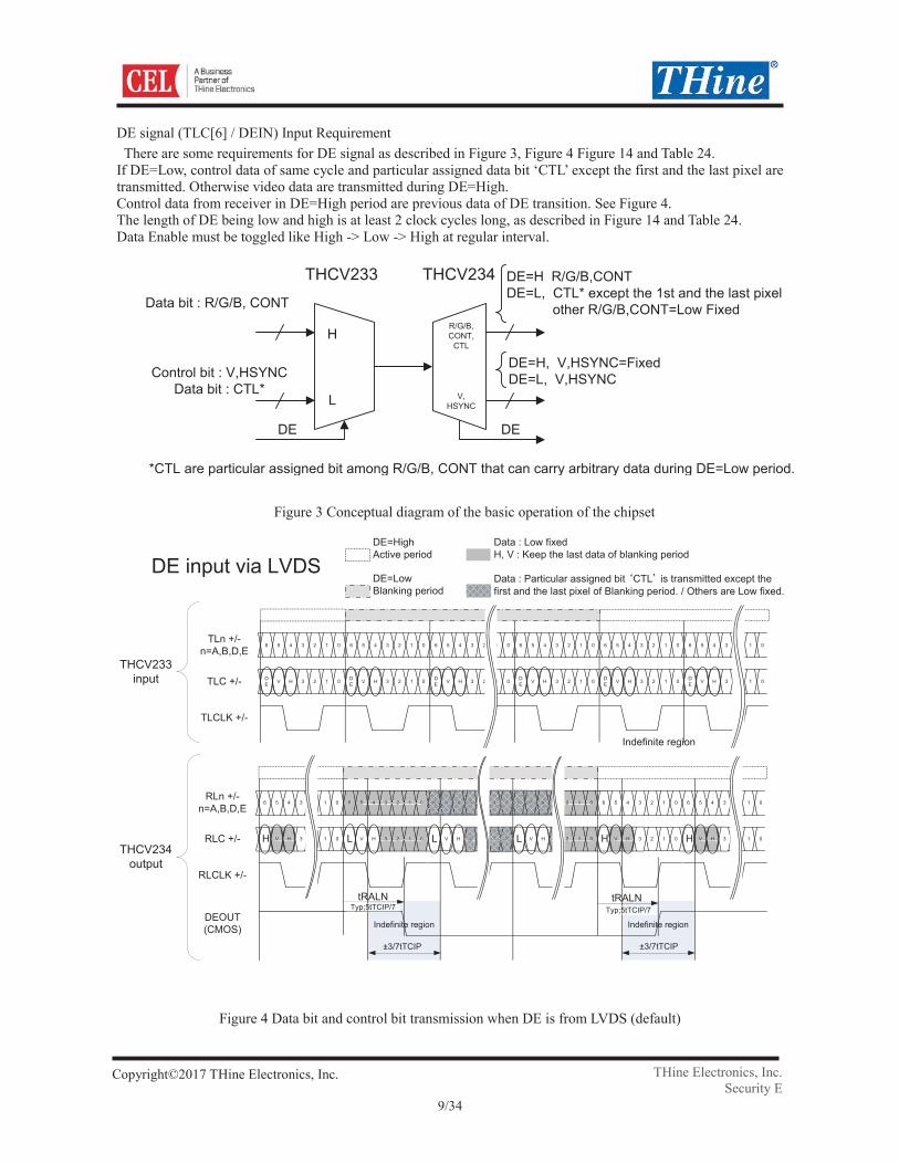
Data bit : R/G/B, CONT
Control bit : V,HSYNCData bit : CTL*
H
L
DE
THCV234THCV233
R/G/B, CONT,
CTL
V,HSYNC
DE=H R/G/B,CONTDE=L, CTL* except the 1st and the last pixel other R/G/B,CONT=Low Fixed
DE=H, V,HSYNC=Fixed DE=L, V,HSYNC
DE
*CTL are particular assigned bit among R/G/B, CONT that can carry arbitrary data during DE=Low period.
TLCLK +/-
6 5 4 3 2 1 0
DE V H 3 2 1 0
TLn +/-n=A,B,D,E
TLC +/-
6 5 4 3 2 1 0
DE V H 3 2 1 0
6 5 4 3 2 1 0
DE V H 3 2 1 0
6 5 4 3 2 1 0
DE V H 3 2 1 0
6 5 4 3 2 1 0
DE V H 3 2 1 0
6 5 4 3 2 1 0
DE V H 3 2 1 0
DE=HighActive period
DE=LowBlanking period
Data : Low fixedH, V : Keep the last data of blanking period
THCV233input
THCV234output
DE input via LVDSData : Particular assigned bit CTL is transmitted except the first and the last pixel of Blanking period. / Others are Low fixed.
RLCLK +/-
6 5 4 3 2 1 0
H V H 3 2 1 0
RLn +/-n=A,B,D,E
RLC +/-
6 5 4 3 2 1 0
L V H 3 2 1 0
6 5 4 3 2 1 0
L V H 3 2 1 0
6 5 4 3 2 1 0
L V H 3 2 1 0
6 5 4 3 2 1 0
H V H 3 2 1 0
6 5 4 3 2 1 0
H V H 3 2 1 0
6 5 4 3 2 1 0
03 2 1 02 1HV HV V H
Indefinite region
Indefinite region
DEOUT(CMOS)
±3/7tTCIP
6666 5555 4 35 4 35 4 34 3 2 12 12 12 1 0000 666 5 4 35 4 35 4 35 4 3333 2 1 01
3333 2 12 12 12 1 0000 3333333
±3/7tTCIP
tRALN tRALN
Indefinite region
Typ;5tTCIP/7Typ;5tTCIP/7

TLCLK +/-
6 5 4 3 2 1 0
X V H 3 2 1 0
TLn +/-n=A,B,D,E
TLC +/-
6 5 4 3 2 1 0
X V H 3 2 1 0
6 5 4 3 2 1 0
X V H 3 2 1 0
6 5 4 3 2 1 0
X V H 3 2 1 0
6 5 4 3 2 1 0
X V H 3 2 1 0
6 5 4 3 2 1 0
X V H 3 2 1 0
DE=HighActive period
DE=LowBlanking period
RLCLK +/-
6 5 4 3 2 1 0
H V H 3 2 1 0
RLn +/-n=A,B,D,E
RLC +/-
6 5 4 3 2 1 0
L V H 3 2 1 0
6 5 4 3 2 1 0
L V H 3 2 1 0
6 5 4 3 2 1 0
L V H 3 2 1 0
6 5 4 3 2 1 0
H V H 3 2 1 0
6 5 4 3 2 1 0
H V H 3 2 1 0
6 4 3 2 1 05 1
03 2 1 02 1HV HV V H
DEIN(CMOS)
THCV233input
THCV234output
DE input via DEINData : Low fixedH, V : Keep the last data of blanking period X Ignored
Indefinite region Indefinite region
DEOUT(CMOS)
±3/7tTCIP
666 5 4 35 4 35 4 35 4 2 12 12 12 666000 5 4 35 45 44 3336 5 4 34 34 3 2 12 11 66000 5 444 33 2 1 01
Data : Particular assigned bit CTL is transmitted except the first and the last pixel of Blanking period. / Others are Low fixed.
333 2 12 12 12 1 0000 3333
tTALN tTALN
±3/7tTCIP
tRALNTyp;5tTCIP/7
tRALNTyp;5tTCIP/7

COL Mode FunctionL 32bit-Data widthH 24bit-Data width
MODE[1:0] Operation modeLL Single-in / Distribution Dual-outLH Single-in / Single-outHL Single-in / Dual-outHH Reserved (forbidden)
MODE[1:0] Operation modeLL Dual-in / Selected single-out (Lane 0)LH Dual-in / Single-outHL Dual-in / Selected single-out (Lane 1)HH Single-in /Single-out

HTPDNLOCKNRX0P/NRX1P/NRX2P/NRX3P/N
Open
THCV234
THCV234
HTPDN
LOCKN
DGLOCK
V-by-One®HS
Transmitter
DGLOCK
HTPDN
LOCKNOpen

TLA6
Vdiff = (TLCLK +) - (TLCLK-)
TLA5 TLA4 TLA3 TLA2 TLA1 TLA0 TLA6 TLA5 TLA4 TLA3 TLA2 TLA1
tTCIPVdiff = 0V
next cyclecurrent cycle
TLA2 TLA1
previous cycle
TLB6 TLB5 TLB4 TLB3 TLB2 TLB1 TLB0 TLB6 TLB5 TLB4 TLB3 TLB2 TLB1TLB2 TLB1
TLC6(DE)
TLC5(V)
TLC4(H) TLC3 TLC2 TLC1 TLC0 TLC3 TLC2 TLC1TLC2 TLC1
TLD6 TLD5 TLD4 TLD3 TLD2 TLD1 TLD0 TLD6 TLD5 TLD4 TLD3 TLD2 TLD1TLD2 TLD1
TLE6 TLE5 TLE4 TLE3 TLE2 TLE1 TLE0 TLE6 TLE5 TLE4 TLE3 TLE2 TLE1TLE2 TLE1
TLA +/-
TLB +/-
TLC +/-
TLD +/-
TLE +/-
Control data bitData Enable
TLC6(DE)
TLC5(V)
TLC4(H)
Data width 32, 24

H (8bit) L (10bit)TLA[0] RLA[0] R[2] R[4] D2TLA[1] RLA[1] R[3] R[5] D3TLA[2] RLA[2] R[4] R[6] D4TLA[3] RLA[3] R[5] R[7] D5TLA[4] RLA[4] R[6] R[8] D6TLA[5] RLA[5] R[7] R[9] D7TLA[6] RLA[6] G[2] G[4] D10TLB[0] RLB[0] G[3] G[5] D11TLB[1] RLB[1] G[4] G[6] D12TLB[2] RLB[2] G[5] G[7] D13TLB[3] RLB[3] G[6] G[8] D14TLB[4] RLB[4] G[7] G[9] D15TLB[5] RLB[5] B[2]*2 B[4]*2 D18TLB[6] RLB[6] B[3]*2 B[5]*2 D19TLC[0] RLC[0] B[4]*2 B[6]*2 D20TLC[1] RLC[1] B[5]*2 B[7]*2 D21TLC[2] RLC[2] B[6]*2 B[8]*2 D22TLC[3] RLC[3] B[7]*2 B[9]*2 D23TLC[4] RLC[4] HSYNC HSYNC HsyncTLC[5] RLC[5] VSYNC VSYNC VsyncTLC[6] RLC[6] DE DE DETLD[0] RLD[0] R[0] R[2] D0TLD[1] RLD[1] R[1] R[3] D1TLD[2] RLD[2] G[0] G[2] D8TLD[3] RLD[3] G[1] G[3] D9TLD[4] RLD[4] B[0]*2 B[2]*2 D16TLD[5] RLD[5] B[1]*2 B[3]*2 D17TLD[6] RLD[6] N/A*1 CONT[1]*2*3 D25*3TLE[0] RLE[0] R[0]*2 D30TLE[1] RLE[1] R[1]*2 D31TLE[2] RLE[2] G[0]*2 D28TLE[3] RLE[3] G[1]*2 D29TLE[4] RLE[4] B[0]*2 D26TLE[5] RLE[5] B[1]*2 D27TLE[6] RLE[6] CONT[2]*2*3 D24*3
*1 N/A: Not available, THCV234 output RLDn[6]=Low.*2 CTL bits, which are carried during DE=Low except the 1st and the last pixel*3 3D flags defined in the V-by-One® HS Standard are assigned to the following bit. V-by-One® HS Standard Packer/Unpacker D[24](3DLR) <=> LVDS T/RLE[6] V-by-One® HS Standard Packer/Unpacker D[25](3DEN) <=> LVDS T/RLD[6]
ChannelPowerDown
THCV233Input
THCV234Output
COL Symbol defined byV-by-One® HS

RS Output swingL Reduced swing (200mV typical)H Normal swing (350mV typical)
CAVDL
TXnP RXnP
TXnN RXnN
Vterm 1.3v
Zdiff=100
C=75200nF
50n=0,1
CAVDL
CAGND
THCV233 THCV234
CMLTransmitter
CMLReceiver
50
C=75200nF
Capacitor on transmitter side is mandatory, while receiver side is optional and recommended.
50
50

3.3V(THCV233 side)
3.3V(THCV233 side)
HTPDN
LOCKN
10k
THCV233 THCV234
10k
3.3V(THCV233 side)
HTPDN
LOCKN
10k
THCV233 THCV234
HTPDN
PRE DescriptionL without Pre-emphasisH with 100% Pre-emphasis
DEOUT OutputL Bit error occurredH No error
THCV233BET BET RS Operation Output Latch select
L L - Normal Operation -H H L NOT latched resultH H H Latched result
THCV234 Condition
FieldBET Operation
THCV233 THCV234
LVDS-CLK
BET=H
TestPatternChecker
Test PatternGenerator DEOUT
Test Point for Field BET
BET=HLatch select

8. Absolute Maximum Ratings
Parameter Symbol Min. Typ. Max. Units1.8v Supply Voltage CAVDL,CPVDL,VDD VDL -0.3 - +2.1 V3.3v Supply Voltage(LAVDH) VDH -0.3 - +4.0 VCMOS Input Voltage - -0.3 - VDH+0.3 VLVDS Receiver Input Voltage - -0.3 - VDH+0.3 VCML Transmitter Output Voltage - -0.3 - VDL+0.3 VOutput Current - -50 - 50 mAStorage Temperature - -55 - +125 °CJunction Temperature - - - +125 °CReflow Peak Temperature/Time - - - +260/10sec °CMaximum Power Dissipation @ 25°C - - - 3.2 W
Parameter Symbol Min. Typ. Max. Units1.8v Supply Voltage(CAVDL,VDD) VDL -0.3 - +2.1 V3.3v Supply Voltage(LAVDH) VDH -0.3 - +4.0 VCMOS Input Voltage - -0.3 - VDH+0.3 VCML Receiver Input Voltage - -0.3 - VDL+0.3 VLVDS Transmitter Output Voltage - -0.3 - VDH+0.3 VOutput Current - -30 - 30 mAStorage Temperature - -55 - +125 °CJunction Temperature - - - +125 °CReflow Peak Temperature/Time - - - +260/10sec °CMaximum Power Dissipation @ 25°C - - - 3.2 W
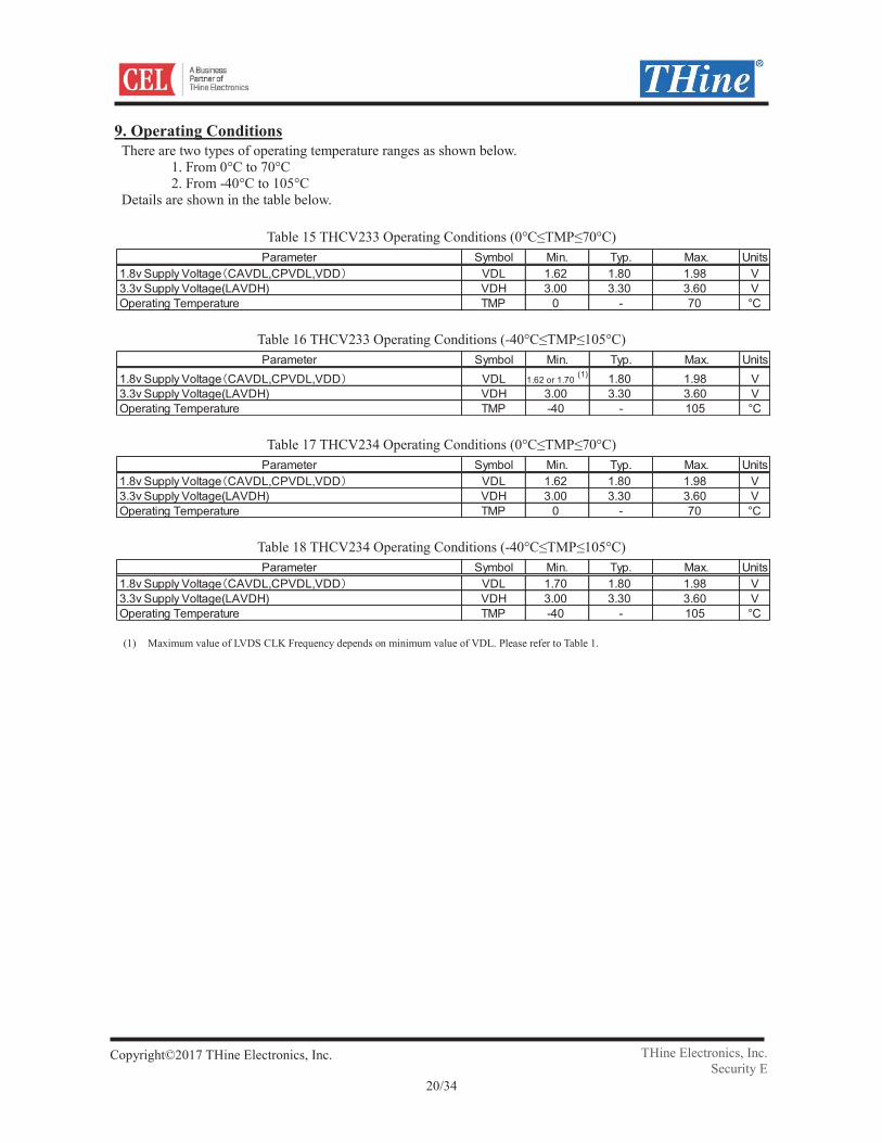
9. Operating Conditions
Parameter Symbol Min. Typ. Max. Units1.8v Supply Voltage CAVDL,CPVDL,VDD VDL 1.62 1.80 1.98 V3.3v Supply Voltage(LAVDH) VDH 3.00 3.30 3.60 VOperating Temperature TMP 0 - 70 °C
Parameter Symbol Min. Typ. Max. Units1.8v Supply Voltage CAVDL,CPVDL,VDD VDL 1.62 or 1.70 (1) 1.80 1.98 V3.3v Supply Voltage(LAVDH) VDH 3.00 3.30 3.60 VOperating Temperature TMP -40 - 105 °C
Parameter Symbol Min. Typ. Max. Units1.8v Supply Voltage CAVDL,CPVDL,VDD VDL 1.62 1.80 1.98 V3.3v Supply Voltage(LAVDH) VDH 3.00 3.30 3.60 VOperating Temperature TMP 0 - 70 °C
Parameter Symbol Min. Typ. Max. Units1.8v Supply Voltage CAVDL,CPVDL,VDD VDL 1.70 1.80 1.98 V3.3v Supply Voltage(LAVDH) VDH 3.00 3.30 3.60 VOperating Temperature TMP -40 - 105 °C

10. Electrical Specifications
Symbol Parameter Conditions Min. Typ. Max. UnitsVIH High Level Input Voltage I,BPU 2.1 - VDH VVIL Low Level Input Voltage I,BPU 0 - 0.7 VVOH High Level Output Voltage O IOH=-8mA 2.4 - VDH V
O IOL=8mA - - 0.4 VO,BPU IOL=4mA - - 0.4 V
IIH Input Leak Current High VIN=VDH -10 - +10 uAIIL Input Leak Current Low VIN=GND -10 - +10 uA
VOL Low Level Output Voltage
Symbol Parameter Conditions Min. Typ. Max. UnitsVTTH LVDS Differential Input High Threshold - - - 100 mVVTTL LVDS Differential Input Low Threshold - -100 - - mV
ITIH LVDS Input Leak Current High TLx+/-=VDH, PDN=Lx=A~E,CLK - - ±10 uA
ITIL LVDS Input Leak Current Low TLx+/-=GND, PDN=Lx=A~E,CLK - - ±10 uA
RTIN LVDS Differential Input Resistance PDN=L 80 100 120 ΩVTOD CML Differential Mode Output Voltage - 200 300 400 mV
PRE=L - 0 - %PRE=H 80 100 120 %PRE=L mVPRE=H mV
ITOH CML Output Leak Current High PDN=L - - ±10 uAITOS CML Output Short Circuit Current VDL=1.8V -90 - - mA
PRE CML Pre-emphasis Level
VTOC CML Common Mode Output Voltage VDL-VTODVDL-2×VTOD
Symbol Parameter Conditions Min. Typ. Max. UnitsVRTH CML Differential Input High Threshold - - - 50 mVVRTL CML Differential Input Low Threshold - -50 - - mV
IRIH CML Input Leak Current High PDN=L, RXnP/N=VDLn=0,1 - - ±10 uA
IRIL CML Input Leak Current Low PDN=L, RXnP/N=GNDn=0,1 - - ±10 uA
IRRIH CML Input Current High RXnP/N=VDL, n=0,1 - - 2 mAIRRIL CML Input Current Low RXnP/N=GND, n=0,1 -6 - - mARRIN CML Differential Input Resistance - 80 100 120 Ω
LVDS Differential Mode Output Voltage (Normal Swing) RL=100Ω, RS=H 250 350 450 mV
LVDS Differential Mode Output Voltage (Reduced Swing) RL=100Ω, RS=L 100 200 300 mV
ΔVROD Change in VROD betweenComplementary Output States RL=100Ω - - 35 mV
VROC LVDS Common Mode Output Voltage RL=100Ω 1.125 1.25 1.375 V
ΔVROC Change in VROC betweenComplementary Output States RL=100Ω - - 35 mV
IROS LVDS Output Short Circuit Current RLx+/-=GND -30 - - mA
IROZ LVDS Output TRI-STATE CurrentPDN=L,RLx+/-=GND, VDHx=A~E,CLK
- - ±10 uA
VROD

Vdiff = (TLCLK +) - (TLCLK -)tTCIP
Vdiff = 0V
next cyclecurrent cycleprevious cycle
TLA +/-
TLB +/-
TLC +/-
TLD +/-
TLE +/-
Control bitData Enable
H H
Symbol Parameter Conditions Min. Typ. Max. UnitsSiSo 10bit, PRE=HPDN=H - - 150 mA
SiDo 10bit, PRE=HPDN=H - - 185 mA
SiDDo 10bit, PRE=HPDN=H - - 225 mA
SiSo 10bit, PRE=HPDN=H - - 12 mA
SiDo 10bit, PRE=HPDN=H - - 12 mA
SiDDo 10bit, PRE=HPDN=H - - 12 mA
ITCCS Transmitter Power DownSupply Current
PDN=LAll Inputs =Fixed LorH - - 170 uA
ITCCW_M Transmitter Supply Current for VDL(Worst Case Pattern as shown in Figure 12)
ITCCW33_M Transmitter Supply Current for VDH(Worst Case Pattern as shown in Figure 12)
Symbol Parameter Conditions Min. Typ. Max. Units
SiSo 10bit, PDN=H - - 90 mA
DiSo 10bit, PDN=H - - 90 mA
DiSSo 10bit, PDN=H - - 90 mA
SiSo 10bit, P PDN=H - - 90 mA
DiSo 10bit, PDN=H - - 90 mA
DiSSo 10bit, PDN=H - - 90 mA
IRCCS Receiver Power DownSupply Current
PDN=LAll Inputs =Fixed LorH - - 150 uA
Receiver Supply Current for VDL(Worst Case Pattern as shown in Figure 12)
Receiver Supply Current for VDH(Worst Case Pattern as shown in Figure 12)IRCCW33_M
IRCCW_M
Symbol Parameter Conditions Min. Typ. Max. UnitstDEH DE=High Duration - 2×tTCIP - - sec
SiSo, SiDDo 2×tTCIP - - secSiDo 4×tTCIP - - sec
tDEL DE=Low Duration
Symbol Parameter Conditions Min. Typ. Max. UnitsCOL=H, Si/So 10 - 111 nsCOL=H, Si/DDo 10 - 50 nsCOL=H, Si/Do 10 - 25 nsCOL=L, Si/So 11.76 - 111 nsCOL=L, Si/DDo 11.76 - 50 nsCOL=L, Si/Do 11.76 - 25 ns
tTCIH LVDS Differential Clock High Time - 2×tTCIP/7 4×tTCIP/7 5×tTCIP/7 nstTCIL LVDS Differential Clock Low Time - 2×tTCIP/7 3×tTCIP/7 5×tTCIP/7 ns
tTCIP=75MHz -440 - 440 pstTCIP=85MHz -390 - 390 pstTCIP=100MHz -330 - 330 ps
tTIP1 LVDS Input Data Position1 - -tSK 0 +tSK nstTIP0 LVDS Input Data Position0 - tTCIP/7-tSK tTCIP/7 tTCIP/7+tSK nstTIP6 LVDS Input Data Position2 - 2×tTCIP/7-tSK 2×tTCIP/7 2×tTCIP/7+tSK nstTIP5 LVDS Input Data Position3 - 3×tTCIP/7-tSK 3×tTCIP/7 3×tTCIP/7+tSK nstTIP4 LVDS Input Data Position4 - 4×tTCIP/7-tSK 4×tTCIP/7 4×tTCIP/7+tSK nstTIP3 LVDS Input Data Position5 - 5×tTCIP/7-tSK 5×tTCIP/7 5×tTCIP/7+tSK nstTIP2 LVDS Input Data Position6 - 6×tTCIP/7-tSK 6×tTCIP/7 6×tTCIP/7+tSK nstTALN LVDS-ALNIN timing tolerance - 0 - 3×tTCIP/7 nstTRF CML Output Rise and Fall Time(20%-80%) - 50 - 150 pstTOSK CML Lane0/1 Output Inter Pair Skew - -2 - 2 UItTCD Input Clock to Output Data Delay SiDDo 10bit 85MHz 143.4 - 150.2 nstTLH VDL On to VDH On Delay - 0 - - nstTPD Power On to PDN High Delay - 0 - - nstTPDL PDN Low Pulse Width - 1 - - mstTPLL0 PDN High to CML Output Delay - - - 10 mstTPLL1 PDN Low to CML Output High Fix Delay - - - 20 nstTNP0 LOCKN High to Training Pattern Output Delay - - - 10 mstTNP1 LOCKN Low to Data Pattern Output Delay - - - 10 ms
tTCIP TLCLK Period
tSK LVDS Receiver Skew Margin

Symbol Parameter Conditions Min. Typ. Max. UnitsCOL=H, Si/So 10 - 111 nsCOL=H, Si/DDo 10 - 50 nsCOL=H, Si/Do 10 - 25 nsCOL=L, Si/SoVDL=1.62V~1.98V 13.33 - 111 ns
COL=L, Si/DDoVDL=1.62V~1.98V 13.33 - 50 ns
COL=L, Si/DoVDL=1.62V~1.98V 13.33 - 25 ns
COL=L, Si/SoVDL=1.7V~1.98V 12.35 - 111 ns
COL=L, Si/DDoVDL=1.7V~1.98V 12.35 - 50 ns
COL=L, Si/DoVDL=1.7V~1.98V 12.35 - 25 ns
tTCIH LVDS Differential Clock High Time - 2×tTCIP/7 4×tTCIP/7 5×tTCIP/7 nstTCIL LVDS Differential Clock Low Time - 2×tTCIP/7 3×tTCIP/7 5×tTCIP/7 ns
tTCIP=75MHz -440 - 440 pstTCIP=85MHz -390 - 390 pstTCIP=100MHz -330 - 330 ps
tTIP1 LVDS Input Data Position1 - -tSK 0 +tSK nstTIP0 LVDS Input Data Position0 - tTCIP/7-tSK tTCIP/7 tTCIP/7+tSK nstTIP6 LVDS Input Data Position2 - 2×tTCIP/7-tSK 2×tTCIP/7 2×tTCIP/7+tSK nstTIP5 LVDS Input Data Position3 - 3×tTCIP/7-tSK 3×tTCIP/7 3×tTCIP/7+tSK nstTIP4 LVDS Input Data Position4 - 4×tTCIP/7-tSK 4×tTCIP/7 4×tTCIP/7+tSK nstTIP3 LVDS Input Data Position5 - 5×tTCIP/7-tSK 5×tTCIP/7 5×tTCIP/7+tSK nstTIP2 LVDS Input Data Position6 - 6×tTCIP/7-tSK 6×tTCIP/7 6×tTCIP/7+tSK nstTALN LVDS-ALNIN timing tolerance - 0 - 3tTCIP/7 nstTRF CML Output Rise and Fall Time(20%-80%) - 50 - 150 pstTOSK CML Lane0/1 Output Inter Pair Skew - -2 - 2 UItTCD Input Clock to Output Data Delay SiDDo 10bit 85MHz 143.4 - 150.2 nstTLH VDL On to VDH On Delay - 0 - - nstTPD Power On to PDN High Delay - 0 - - nstTPDL PDN Low Pulse Width - 1 - - mstTPLL0 PDN High to CML Output Delay - - - 10 mstTPLL1 PDN Low to CML Output High Fix Delay - - - 20 ns
tTNP0 LOCKN High to Training Pattern OutputDelay - - - 10 ms
tTNP1 LOCKN Low to Data Pattern OutputDelay - - - 10 ms
tSK
tTCIP
LVDS Receiver Skew Margin
TLCLK Period

Symbol Parameter Conditions Min. Typ. Max. UnitsCOL=H 333 tTCIP/30 3704 psCOL=L 294 tTCIP/40 2778 ps
tRISK CML Lane0/1 Input Inter Pair Skew Margin - - - 15 UItRLVT LVDS Differential Output Transition Time - - 0.6 1.5 nstROP1 LVDS Output Data Position1 SiSo 10bit 85MHz -0.2 0 0.2 nstROP0 LVDS Output Data Position0 SiSo 10bit 85MHz tTCIP/7-0.2 tTCIP/7 tTCIP/7+0.2 nstROP6 LVDS Output Data Position6 SiSo 10bit 85MHz 2×tTCIP/7-0.2 2×tTCIP/7 2×tTCIP/7+0.2 nstROP5 LVDS Output Data Position5 SiSo 10bit 85MHz 3×tTCIP/7-0.2 3×tTCIP/7 3×tTCIP/7+0.2 nstROP4 LVDS Output Data Position4 SiSo 10bit 85MHz 4×tTCIP/7-0.2 4×tTCIP/7 4×tTCIP/7+0.2 nstROP3 LVDS Output Data Position3 SiSo 10bit 85MHz 5×tTCIP/7-0.2 5×tTCIP/7 5×tTCIP/7+0.2 nstROP2 LVDS Output Data Position2 SiSo 10bit 85MHz 6×tTCIP/7-0.2 6×tTCIP/7 6×tTCIP/7+0.2 nstRALN LVDS-ALNOUT timing accuracy - 2×tTCIP/7 5×tTCIP/7 8tTCIP/7 nstRDC Input Data to Output Clock Delay SiSo 10bit 808×tRBIT+8 - 808×tRBIT+14.5 nstRLH VDL On to VDH On Delay - 0 - - nstRPD Power On to PDN High Delay - 0 - - nstRPDL PDN Low Pulse Width - 1.0 - - mstRHPD0 PDN High to HTPDN Low Delay - - - 1 ustRHPD1 PDN Low to HTPDN High Delay - - - 1 us
tRPLL0 Training Pattern Input to LOCKN LowDelay - - - 10 ms
tRPLL1 PDN Low to LOCKN High Delay - - - 10 ustRLCK0 LOCKN Low to LVDS Output Delay - - - 1 mstRLCK1 LOCKN High to LVDS HighZ Delay - - - 0 ns
tRBIT Unit Interval
Symbol Parameter Conditions Min. Typ. Max. UnitsCOL=H 351 tTCIP/30 3704 psCOL=L 351 tTCIP/40 2778 ps
tRISK CML Lane0/1 Input Inter Pair Skew Margin - - - 15 UItRLVT LVDS Differential Output Transition Time - - 0.6 1.5 nstROP1 LVDS Output Data Position1 SiSo 10bit 85MHz -0.2 0 0.2 nstROP0 LVDS Output Data Position0 SiSo 10bit 85MHz tTCIP/7-0.2 tTCIP/7 tTCIP/7+0.2 nstROP6 LVDS Output Data Position6 SiSo 10bit 85MHz 2×tTCIP/7-0.2 2×tTCIP/7 2×tTCIP/7+0.2 nstROP5 LVDS Output Data Position5 SiSo 10bit 85MHz 3×tTCIP/7-0.2 3×tTCIP/7 3×tTCIP/7+0.2 nstROP4 LVDS Output Data Position4 SiSo 10bit 85MHz 4×tTCIP/7-0.2 4×tTCIP/7 4×tTCIP/7+0.2 nstROP3 LVDS Output Data Position3 SiSo 10bit 85MHz 5×tTCIP/7-0.2 5×tTCIP/7 5×tTCIP/7+0.2 nstROP2 LVDS Output Data Position2 SiSo 10bit 85MHz 6×tTCIP/7-0.2 6×tTCIP/7 6×tTCIP/7+0.2 nstRALN LVDS-ALNOUT timing accuracy - 2×tTCIP/7 5×tTCIP/7 8×tTCIP/7 nstRDC Input Data to Output Clock Delay SiSo 10bit 808×tRBIT+8 - 808×tRBIT+14.5 nstRLH VDL On to VDH On Delay - 0 - - nstRPD Power On to PDN High Delay - 0 - - nstRPDL PDN Low Pulse Width - 1.0 - - mstRHPD0 PDN High to HTPDN Low Delay - - - 1 ustRHPD1 PDN Low to HTPDN High Delay - - - 1 us
tRPLL0 Training Pattern Input to LOCKN LowDelay - - - 10 ms
tRPLL1 PDN Low to LOCKN High Delay - - - 10 ustRLCK0 LOCKN Low to LVDS Output Delay - - - 1 mstRLCK1 LOCKN High to LVDS HighZ Delay - - - 0 ns
Unit IntervaltRBIT

11. AC Timing Diagrams and Test Circuits
TLx6
Vdiff = (TLCLK+) - (TLCLK-)
x=A,B,C,D,E
TLx5 TLx4 TLx3 TLx2 TLx1 TLx0 TLx6 TLx5 TLx4 TLx3 TLx2 TLx1Vdiff = (TLx +) - (TLx -)
tTCIP
Vdiff = 0V
tTIP1
tTIP0
tTIP6
tTIP5
tTIP4
tTIP3
tTIP2
Vdiff = (TLCLK +) - (TLCLK -) Vdiff = 0V
tTCIH tTCIL
Vdiff = (TLCLK0+) (TLCLK0-)
Vdiff = (TLC0+) (TLC0-)
DE DE DE DE DE DE
tDEH tDEL

RLx6
Vdiff = (RLCLK +) - (RLCLK-)
x=A,B,C,D,E
RLx5 RLx4 RLx3 RLx2 RLx1 RLx0 RLx6 RLx5 RLx4 RLx3 RLx2 RLx1Vdiff = (RLx +) - (RLx-)
tROP1
tROP0
tROP6
tROP5
tROP4
tROP3
tROP2
tTCIP
Vdiff = 0V
RL=1005pF
20%
80%
RLx+
RLx-
x=A,B,C,D,E
Vdiff = (RLx +) - (RLx-)
tRLVT tRLVT

TXnP
TXnN
n=0,1
100nF
100nF
< 5mm
20%
80%
Vdiff = (TXnP) - (TXnN)
tTRF tTRF
Vdiff = (TX0P) - (TX0N)
Vdiff = (TX1P) - (TX1N)
tTOSK
Vdiff = (RX0 +) - (RX0-)
Vdiff = (RX1 +) - (RX1-)
tRISK
50
50
Vdiff = 0V
Vdiff = 0V
Vdiff = 0V
Vdiff = 0V

Vdiff = (TLCLK +) - (TLCLK -) Vdiff = 0V
tTCD
Vdiff = (TX0 +) - (TX0-)
Vdiff = (RX0 +) - (RX0-)
Vdiff = 0V
tRDC
pixel 1st bit
pixel 1st bit
Vdiff = (RLCLK +) - (RLCLK -)

Power OnVDH
TLCLK +/-
HTPDN Low-level
PDN
LOCKN
RX0P/N
Fix to VDL Trainingpattern
Normalpattern
Trainingpattern
tTPLL0 tTNP1 tTNP0 tTPLL1
HTPDN
PDN
LOCKN
Trainingpattern
Normalpattern
tRHPD0
tRPLL0 tRPLL1
tRHPD1
TX0P/N
RLx +/-
High Z
tRLCK0 tRLCK1
Data PatternTLx +/-
3.0V
tTPD
tRPD
x=A,B,C,D,E
High Z Valid DataPattern
RLCLK +/-
x=A,B,C,D,E
Power OnVDL 1.62V
tTLH
Power OnVDH
3.0V
Power OnVDL 1.62V
tRLH
THCV233
THCV234
tTPDL
tRPDL

VDD
LVDS input bufferInternal circuit of THCV233
Low VDD
LVDS Tx
THCV233
orLVDS Txintegrated
device
LVDS Tx side PCB LVDS Rx side PCB

THCV233
HTPDN
LOCKN
THCV233
HTPDN
LOCKN
THCV234
HTPDN
LOCKN
DGLOCK
THCV234
HTPDN
LOCKN
DGLOCK
SourceDevice
DestinationDeviceEx. synchronized Time diff. comes up
clkin.1
clkin.2
clkout.1
clkout.2
Internal processing time tTCDInternal processing time tRDC
FIFO
FIFO
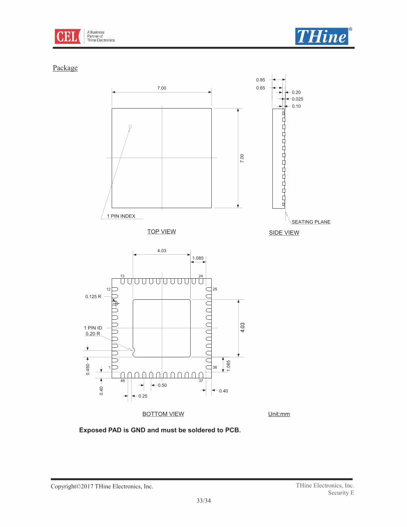
Exposed PAD is GND and must be soldered to PCB.
4.03
7.00
7.00
0.25
0.500.40
1.08
5
1.085
0.40
0.45
0
0.125 R
0.85
0.650.200.0250.10
Unit:mm