TESTING - UC Santa Barbara
110
Transcript of TESTING - UC Santa Barbara

Delay Fault Testing for VLSI Circuits


DELAY FAULT TESTING FORVLSI CIRCUITS
ANGELA KRSTICDepartment of Electrical and Computer EngineeringUniversity of CaliforniaSanta Barbara CA
KWANGTING CHENGDepartment of Electrical and Computer EngineeringUniversity of CaliforniaSanta Barbara CA
Kluwer Academic PublishersBostonDordrechtLondon

Contents
Preface vii
Acknowledgments ix
Introduction xiAngela Krstic
TEST APPLICATION SCHEMES FOR DELAY FAULTS
Combinational Circuits
Sequential Circuits Enhanced scan testing Standard scan testing Slowfastslow clock testing Atspeed testing
Testing High Performance Circuits Using Slower Testers Slowfastslow testing strategy on slow testers Atspeed testing strategy on slow testers
Summary
DELAY FAULT MODELS
Transition Fault Model
Gate Delay Fault Model
Path Delay Fault Model
Segment Delay Fault Model
Line Delay Fault Model
Summary
MOTIVATIONS FOR DELAY TESTING
Summary
PATH DELAY FAULT CLASSIFICATION
Sensitization Criteria Robust testable path delay faults Nonrobust testable path delay faults Validatable nonrobust testable path delay faults Functional sensitizable path delay faults
v
vi DELAY FAULT TESTING FOR VLSI CIRCUITS
Path Delay Faults that do Not Need Testing Robust vs robust dependent path delay faults Functional irredundant vs functional redundant path delay faults Path classication based on input sort heuristic Path classication based on using single stuckat fault tests Primitive vs nonprimitive path delay faults
Multiple Path Delay Faults and Primitive Faults
Summary
DELAY FAULT SIMULATION
Transition Fault Simulation
Gate Delay Fault Simulation
Path Delay Fault Simulation
Segment Delay Fault Simulation
Summary
TEST GENERATION FOR PATH DELAY FAULTS
Robust Tests
High Quality NonRobust Tests Algorithm for generating nonrobust tests with high robustness
Validatable NonRobust Tests
High Quality Functional Sensitizable Tests
Tests for Primitive Faults Cosensitizing gates Merging gates Identifying FS paths not involved in any primitive fault Primitive faults of cardinality
Summary
DESIGN FOR DELAY FAULT TESTABILITY
Robust Delay Fault Testability
Design for Primitive Delay Fault Testability
Summary
SYNTHESIS FOR DELAY FAULT TESTABILITY
Synthesis for Robust Delay Fault Testability
Synthesis for Primitive Delay Fault Testability
Summary
CONCLUSIONS AND FUTURE WORK
References

Preface
This is an example preface This is an example preface This is an examplepreface This is an example preface
This is a preface section
This is an example of a preface This is an example preface This is an examplepreface
ANGELA KRSTIC
vii

This book is dedicated to my
daughter

Acknowledgments
text
ix


INTRODUCTIONAngela Krstic
xi


TEST APPLICATION SCHEMES FOR
VLSI CIRCUITS
Unlike stuckat fault testing delay testing is closely tied to the test applicationstrategy This means that before tests for delay faults are derived it is necessaryto know how these tests will be applied to the circuit The testing strategydepends on the type of the circuit combinational scan nonscan or partial scansequential circuit as well as on the speed of the testing equipment Ordinarilytesting delay defects requires that the test vectors be applied to the circuit atits intended operating speed However since high speed testers require hugeinvestments testers currently used in test facilities are several times slower thanthe new designs that need to be tested on them Testing high speed designs onslower testers requires special test application and test generation strategies
In this chapter we focus on dierent test application schemes for combinational and sequential circuits We describe techniques used for testing scanas well as nonscan designs Also wee address the issue of testing high speeddesigns using slow testers and describe some of the currently available solutionsto this problem
COMBINATIONAL CIRCUITS
To observe delay defects it is necessary to create and propagate transitionsin the circuit Creating transitions requires application of a vector pair V hv vi The rst vector initializes the circuit while the second vector causesthe desired transitions The test application scheme for combinational circuits

DELAY FAULT TESTING FOR VLSI CIRCUITS
is shown in Figure In normal operation only one clock is used to controlthe input and output latche system clock and its period is Tc In testingmode the input nd output latches are controlled by two dierent clocks theinput and output clock respectively The period of these clocks Ts is assumedt be larger than Tc The input and output clocks are skewed by an amountequal to Tc The rst vector v is applied to the primary inputs at time t
inputs input latches
outputlatches
outputs
output clockinput clock
input clock
output clockTs T c
t 0 t 1 t 2
combinational circuit
Figure Testing scheme for combinational circuits
The second vector v is applied at time t Time Ts t t is assumedto be sucient for all values in the circuit to stabilize under the rst vectorAfter the second vector is applied the circuit is allowed to run for one clockcycle until time t where t t Tc At time t the primary output valuesare observed and compared to a prestored response of a faultfree circuit todetermine if there is a defect
SEQUENTIAL CIRCUITS
Most of the delay testing research has concentrated on testing combinationalcircuits Testing delay faults in sequential circuits is signicantly more dicultthan testing delay faults in combinational circuits This is because application of an arbitrary vector pair is not possible to nonscan or standard scansequential circuits Figure a illustrates the model of a sequential circuitIts operation can be represented using an iterative array of the combinationallogic shown in Figure b Each copy of the combinational logic is called atimeframe The present state PS values in timeframe k correspond to thenext state NS values in timeframe k In case of a sequential circuit avector pair V hv vi can be represented as pair V hi s i si wherei i are the values of the primary input lines s s are values of the present

TEST APPLICATION SCHEMES FOR DELAY FAULTS
NSPS
POPI
NSPS
POPI
NSPS
POPIComb.
logic
Comb.
logic
Comb.
logic
NSPS
POPI
FFs
Comb.
logic
(a)
(b)
time-frame ktime-frame k-1 time-frame k+1
Figure Model for sequential circuits
state lines and symbol denotes concatenation of bit vectors Thereforevector i is required to produce s as the next state of the sequential machineThere are several commonly used testing strategies for sequential circuits
enhanced scan functional justication and scan shifting for standard scan slowfastslow strategy and atspeed strategy for nonscan or partial can designs
Enhanced scan testing
To solve this problem Dervisoglu and Strong propose using memory elements that can store two bits of state instead of just one Such ipops arecalled enhanced scan ipops The disadvantages of using enhanced scanipops are high area overhead and long test application time
Standard scan testing
Generating tests for delay faults for standard scan designs corresponds to atwo timeframe sequential circuit test generation In the rst time frame allprimary inputs and present state lines are fully controllable In the secondtimeframe only the primary inputs are fully controllable Testing schemesfor standard scan have been proposed in literature Thesetechniques use functional justication also called broadside test orscan shifting also called skewedload test to obtain the secondvector In functional justication the second vector represents the set of next

DELAY FAULT TESTING FOR VLSI CIRCUITS
state values obtained after the application of the rst vector In scan shiftingthe second vector is obtained by shifting the contents of the scan chain by onebit after the application of the rst vector Figure illustrates the functionaljustication and scan shifting concepts
mode
combinational
logic
combinational
logic
Mux
Mux
FF
FF
mode
Scan shifting
Functional justification
Figure Standard scan design testing schemes
Cheng et al propose a delay test generation algorithm for standard scandesigns It is modied from a PODEMbased combinational test generatorThe modications involve a two timeframe expansion of the combinationallogic of the circuit and the use of backtracking heuristics tailored to detectingdelay faults The present state values for the second vector are generated usingfunctional justication or scan shifting A fault that is redundant under scanshifting might be testable under functional justication and vice versa On theaverage the test generation complexity is lower when scan shifting rather thanfunctional justication is usedThe order of ipops in the scan chain cannot aect the fault coverage
when functional justication is used However when scan shifting is appliedthe order of ipops in the scan chain aects the fault coverage To nd agood order of ipops in the scan chain Cheng et al rst run the testgeneration algorithm for standard scan designs using functional justicationIf the fault is not detectable using functional justication test generation inenhanced scan mode is tried The test generator attempts to have as manydont care entries as possible in the present state lines in the second vectorof the two vector sequence Once the test pair hv vi hi s i siis generated a set of constraints on the scan ordering is computed Theseconstraints if satised guarantee that s can be obtained by scan shifting ofv in standard scan In general if the value of ipop FFi is in s andthe value of ipop FFj is in s then the constraint is that the ipopFFi cannot be the immediate predecessor of ipop FFj in the scan chain Ifthe circuit has n ipops the constraints can be recorded using a quadraticmatrix A of size n Initially all entries in this matrix are set to zero Given

TEST APPLICATION SCHEMES FOR DELAY FAULTS
a test vector pair for some target fault if ipop FFi is not allowed to bethe immediate predecessor of ipop FFj in the scan chain then entry Aij isincreased by one The matrix A is updated after each fault in the fault list isprocessed until the fault list becomes empty The nal value Aij represents thenumber of faults that will not be detected by scan shifting if ipop FFi is thepredecessor of ipop FFj under the vector set used to construct the matrixA The scan ordering is determined such that most of the constraints in matrixA are satised Since a delay fault can have more than one test and only oneof the tests is used to construct the matrix A the fault might be detected evenif the constraints in matrix A have not been completely satised
Even with an ecient order of the ipops in the scan chain a certainnumber of faults that can be detected under enhanced scan design cannot bedetected under standard scan design To increase the fault coverage Cheng atal propose partial enhanced scan design In this design methodologya subset of ipops is selected and made enhanced scan The present statelines of enhanced scan ipops are fully controllable in both timeframes intest generation Given a set of faults that are testable under enhanced scanbut are redundant under functional justication or scan shifting scheme witha given ordering of ipops the proposed heuristic attempts to minimize thenumber of ipops to be made enhanced scan in order to achieve a speciedfault coverage
Slowfastslow clock testing
Testing a fault in nonscan or partial scan sequential circuits requires a sequenceof vectors These vectors correspond to three dierent phases of the test generation process fault initialization fault activation and fault propagation Faultinitialization sets the signal values to the required values for fault activationIn the fault propagation phase the fault eect is propagated from a next stateline to some primary output Fault initialization and fault propagation requirea test sequence while the fault activation requires a vector pair The existenceof delay defects in the initialization and propagation phases can interfere withactivation or the observation of the fault A common solution is to apply aslowfastslow clock testing strategy It assumes that the vectors for initialization and propagation of the fault eect are applied at a slow speed such thatthe circuit can be considered delay faultfree in these test phases In the activation phase the rst vector is applied under the slow clock while the secondvector is applied at the rated speed Figure illustrates the slowfastslowtesting strategy
Testing methodologies for nonscan sequential designs using the slowfastslow scheme have been proposed in The methodology proposedby Devadas is based on extracting the complete or partial state transitiongraph A known reset state is required Due to the need for extracting thestate transition graph this methodology cannot handle large circuits Agrawalet al propose inserting a logic block into the sequential circuit netlist foreach fault such that testing a delay fault becomes equivalent to testing a certain

DELAY FAULT TESTING FOR VLSI CIRCUITS
NSPS
POPI
Slow clock Rated clock Slow clock
Fault PropagationFault ActivationFault Initialization
NSPS
POPI
NSPS
POPI
NSPS
POPI
NSPS
POPI
NSPS
POPI Comb.
logic
Comb.
logic
Comb.
logic
Comb.
logic
Comb.
logic
Comb.
logic
Figure Slowfastslow testing strategy
stuckat fault Chakraborty et al propose a delay test generator based onthe iterative logic array model for sequential circuits It considers two timeframes at a timeUsing a slow clock in fault initialization and fault propagation phases sig
nicantly simplies the test generation for delay faults However the needfor two clocks slow and fast complicates the test application Testing delayfaults in nonscan or partial scan design is further complicated by the fact thatit is usually not practical to apply a single fault assumption for delay faultsTherefore in slowfastslow clock testing scheme it could happen that at theend of the fault activation phase more than one ipop latches a faulty valueThe test generator has to account for this possibility in the fault propagationphase Chakraborty et al consider dierent initial conditions for the faultpropagation phase
Atspeed testing
Atspeed testing strategy assumes that the fault is initialized activated andpropagated under a fast clock Therefore delay faults are present in all threephasesAtspeed testing strategies for sequential circuits have been proposed in
Pomeranz et al assume that multiple delay faults can simultaneouslybe present in the circuit and develop a value system for testing delay faultsunder these conditions In their experiments several fast clocks up to wereembeded in sequences of slow clocks The atspeed test methodology proposedby Cheng uses a single fault assumptionSome faults that are untestable under the slowfastslow clock testing scheme
might become testable under the atspeed scheme and vice versa
TESTING HIGH PERFORMANCE CIRCUITS USING SLOWER
TESTERS
Testing a design at its intended operating speed requires high speed testersHigh cost of fast testers makes it impossible for the testers to follow the designsin terms of speed increase The problem of testing high performance circuitswithout high speed testers has been addressed by a number of researchers

TEST APPLICATION SCHEMES FOR DELAY FAULTS
The proposed strategies include tester pin multiplexing
Control
Variabledelay
FFs
Clock
Combinational logic
Figure Inserting a controllable delay in the combinational logic
builtin selftest use of a high speed clock and shift registers use ofspecial test xtures reducing the supply voltage use of onchip testcircuitry for testing high bandwidth memories The technique proposed byAgrawal et al involve adding extra logic to the combinational logic such thatthe speed of the circuit in the testing mode becomes slower and comparable tothe speed of testers The amount of the added delay can be controlled by a testinput signal Figure illustrates the concept The extra logic for inserting
Clock
Control
Control
In
Out
(b)
T
A B C
(a)
Figure A controlled delay element and a waveform applied to the control input
the variable delay should be controllable have a minimum normal

DELAY FAULT TESTING FOR VLSI CIRCUITS
mode delay be testable and use minimum logic The following exampledescribes one possible implementation of such logic
Example Consider the circuit in Figure a When the control inputis set to the input signal propagates to the output When the control inputis the output holds its value During normal operation the control inputis held at If single clock masterslave ipops are assumed and the clockwaveform is as shown in Figure b the falling edge A is the time when thedata is transferred from the master to slave ipop and the data stored in theslave ipop is applied to the combinational logic The new data stored in theslave ipop will stay there until the next falling edge C The rising edge B
opens the master ipop to the input data The time between the two fallingedges A and C represents the clock period T Figure b also shows thewaveform for the control signal for the inserted logic At the falling edge A ofthe clock control signal drops to and blocks the application of the data fromthe slave ipop to the combinational logic After a delay the control signalrises to and thus allows the value from the slave ipop to be applied tothe combinational logic From Figure b it is clear that if T represents theclock period of the tester then the clock period of the circuit can at most beTrated T In the test mode delay can be varied by changing the pulsewidth of the waveform
The use of slowfastslow and atspeed testing schemes for testing high performance designs on slow testers has been discused by Krstic et al Theyassume that the speed of the circuit is k k is a positive integer times higherthan the speed of the tester and that an internal fast clock matching the speedof the circuit is available If there is no fast clock available on the tester thefast clock can be generated using frequency multiplier and the testers clock
Slowfastslow testing strategy on slow testers
The slowfastslow testing scheme can under certain constraints be used to testhigh performance circuits on low speed testers In this scheme the testable setof faults is aected by the presence or absence of latches on primary outputsThis is because to observe a fault after activation it has to be propagated tosome primary output
Definition Faults that in the activation timeframe can be propagated onlyto a primary output are called POlogic faults
Definition Faults that in the activation timeframe can be propagated toeither a primary output or to a next state line and faults that in the activationtimeframe can be propagated only to a next state line are called NSlogic faults
Next we consider the use of slowfastslow scheme on slow testers for testingnonscan scan and partial scan designs

TEST APPLICATION SCHEMES FOR DELAY FAULTS
Testing nonscan designs The test application scheme for nonscan designs with latched PIPO is shown in Figure a The primary inputs canbe latched but it is not essential The primary inputs are applied and the primary outputs are observed at the testers speed The testers clock is also usedin the slow phases fault initialization and fault propagation The testers clockis assumed to be slow enough for the circuit to be faultfree in these phasesFault activation is performed with a fast clock
Example Consider the waveform in Figure b It illustrates the casewhen when the testers clock is times slower than the operating speed of thecircuit under test ie k Also it is assumed that the test sequence forthe target fault consists of two initialization vectors v and v one activationvector v and two propagation vectors v and v Initialization vectors vand v are applied at times t and t respectively After the application of theactivation vector at time t the values of the primary outputs and next statesare latched at time t Next the propagation vectors v and v are appliedat times t and t respectively Finally at time t the primary outputs areobserved
(b)
(a)
Circuitobserved at tester’s clock rate
POL LPI
Delayelements
applied at tester’s clock rate
k * tester’s clock
tester’s clock
2*tester’s clock
tester’s clock
2t 3t t 5 t 6 t 7t 4t 1
Figure Nonscan designs with latched PIPO
Since the primary outputs can be latched at the end of the activation phasethis methodology can test both NSlogic and POlogic faults

DELAY FAULT TESTING FOR VLSI CIRCUITS
When the primary outputs are not latched POlogic faults might not betestable on a slow tester using slowfastslow testing scheme Only faults thatare larger than a certain size can be tested For example POlogic faults inthe circuit in Figure a have to be larger than t t to be testable
Testing Scan Designs Test application scheme that allows testing highspeed scan designs on a low speed tester is illustrated in Figure a Thetesters clock is used for applying the primary inputs for the scanin operationas well as for observation of the primary outputs and next state values iescanout operation The fast clock is used for latching the values into primaryoutputs and next states
Example The waveform in Figure b illustrates the case when k First the present state values v are scanned into the registers Next vectorv i s is applied at time t If standard scan is used the state values sof the second vector can be obtained through functional justication Thesecond vector v is is applied at time t Time tt is assumed to besucient for the signal values to settle to their nal values after the applicationof vector v and before application of v Next one fast clock cycle is appliedand at time t the values of the primary outputs and next states are latchedAt time t the primary outputs can be observed and the scanout operationcan start Then the same cycle repeats for the next test
Since the primary outputs can be latched after the application of the fast clockboth POlogic and NSlogic faults can be tested using this scheme However ifthe scan circuit in Figure a does not have latches at the primary outputsfrom the waveform in Figure b we get that POlogic faults have to belarger than t t in order to be detectable
Testing Partial Scan Designs Testing scheme for partial scan designs represents a combination of the schemes described for nonscan and scan designsThe testing strategy depends on the target fault For faults that can be testedthrough paths between the nonscan ipops faults between nonscan ipopsand POs and faults between PIs and nonscan ipops the testing process issimilar to the process described for faults in nonscan designs It consists ofinitialization activation and propagation phase However since some of thememory elements are scanned the initialization and propagation phases mightbe shorter than in the nonscan case For faults that can be tested throughpaths between the scanned ipops faults between scanned ipops and POsand faults between PIs and scanned ipops the testing strategy is the sameas the one described for scan designs
Atspeed testing strategy on slow testers
Conventional atspeed testing strategies for sequential circuits assumethat the inputs are applied and the outputs are observed at the circuits rated

TEST APPLICATION SCHEMES FOR DELAY FAULTS
Circuit
k * tester’s clock
mode S
out
in
S
Delay
elements
tester’s clock
(b)
t 1 t 2 t 4
tester’s clock
2*tester’s clock
t 3
PIapplied at tester’ clock rate
L POobserved at tester’s clock rate
L
(a)
Figure Scan designs with latched PIPO
speed This is impossible to do on a low speed tester Krstic et al propose an atspeed methodology that accommodates the slow speed of the testerFigure illustrates the proposed atspeed scheme The inputs to the circuitare applied and the outputs are observed at the slow testers rate Using theinternal fast clock makes the circuit go through k states between applying theinputs and observing the outputs This is equivalent to saying that the sameset of primary input values are applied for k clock cycles and that the primaryoutputs are observed only at the end of each kth cycle Since the circuit runsatspeed between each application of inputs and observation of outputs delayfaults are constantly present in the circuit
Example Figure a illustrates the proposed atspeed testing schemefor k The same set of primary input values is applied for three fast clockcycles and the primary outputs are only observed after the third cycle Thedelay elements are clocked with the fast clock and the circuit passes throughthree dierent states before the application of the next set of primary inputs
Since the observation of the outputs is performed at the testers speed theexistence or nonexistence of latches at the primary outputs does not aectwhich faults can be tested using this atspeed scheme This means that the

DELAY FAULT TESTING FOR VLSI CIRCUITS
Fast clock
observed at tester’s clock rateCircuitapplied at tester’s clock ratePI PO
Delay
elements
tester’s clock frequency multiplier
Figure Atspeed testing strategy for slow testers
PI
PS
POComb.
ckt
Comb.
ckt
Comb.
ckt
elementsDelay
NSNS PS NS PS
(a)
t 2 t 3 t 4
(b)
3* tester’s clock
tester’s clock
t 1
Figure Atspeed testing scheme for k
proposed atspeed scheme can be used to test POlogic faults that cannot betested using slowfastslow schemeNext we consider the application of the atspeed testing scheme to nonscan
scan and partial scan designs

TEST APPLICATION SCHEMES FOR DELAY FAULTS
Testing NonScan Designs Let the design in Figure a be a nonscandesign and consider the waveform shown in Figure b At time t vectorv i s is applied to the circuit Next at time t the primary inputvalues stay unchanged but the state values have changed Therefore at timet vector v i s is applied to the circuit Similarly at time t vector v i s is applied Finally at time t the primary outputs can be observedA new vector v i s is applied to the circuit at time t and the cyclerepeats In this scheme if the test sequence contains n test vectors where nis a positive integer the circuit actually changes k n states For examplethe circuit in Figure a must go through or or states Thereforethe test generation process for this atspeed testing strategy has to be dierentthan the test generation process for atspeed schemes that assume fast testers
Testing Scan Designs Let the design in Figure a be a scan designand consider the waveform shown in Figure b The application of primaryinputs scanin scanout and observation of the primary output values areperformed at the testers speed However between the scanin and scanoutoperations the circuit is allowed to run with the fast clock and it goes throughthree states while the primary inputs are kept constant At time t the rstset of state values s is assumed to be already scannedin and i is appliedat the primary inputs The state values for the second and third vector v i s and v i s are obtained through functional justication andthese vectors are applied at times t and t respectively At time t the valuesof the primary outputs are observed and the scanout operation starts Thetest sequence for scan designs contains k vectors
Testing Partial Scan Designs As with slowfastslow scheme the atspeedtesting strategy for partial scan designs can be described as a combination oftesting strategies for scan and nonscan designs depending on the target fault
Since in this atspeed testing strategy the primary outputs are observed onlyafter each kth cycle the signal observability is smaller than if the primaryoutputs are observed after each cycle Also since the primary inputs are keptunchanged for k clock cycles the controllability of the signals is negativelyaected as well This can lead to lower fault coverage than if a high speedtester was available Therefore the described atspeed technique should not beused as a standalone technique Instead it can be combined with the slowfastslow testing strategy to obtain higher overall fault coverage In the casewhen there are no latches on the primary outputs the atspeed technique canbe used to test POlogic faults that would stay untestable under slowfastslowstrategy In addition some NSlogic faults might also be untestable by a slowfastslow scheme but testable by the atspeed scheme The proposed atspeedscheme can be used to detect them as well Also there exist faults that canbe tested by both slowfastslow testing strategy and by the atspeed strategyIf these two strategies require that the circuit passes through a comparable

DELAY FAULT TESTING FOR VLSI CIRCUITS
number of states when testing a given fault the atspeed scheme would clearlybe superior in terms of the testing time
Summary
Test application strategy is integral part of delay test generation This is especially true for testing sequential designs for which several dierent strategiesexist Enhanced vs standard scan schemes show the tradeos between theoverhead in area and test application time versus fault coverage Enhaced scanrequires high area and test application time overhead but it also results in ahigher fault coverage than standard scan techniques In slowfastslow testingscheme the assumption that the circuit is faultfree in the fault initializationand propagation phases greatly reduces the complexity of test generation butit complicates the test application process when compared to the atspeedtesting schemeAn important factor in delay fault test generation is also the testers speed
The speed of the testers usually lags behind the speed of the new designsTherefore developing new techniques that would allow testing high speed designs on slower testers is of great practical importance

DELAY FAULT MODELS
The focus of this chapter is on the ways to model delay faults Five delay faultmodels are considered transition fault model gate delay fault model pathdelay fault model segment delay fault model and line delay fault model It isassumed that each gate can have an arbitrary fall rise delay from each inputto the output pin Also the interconnects are assumed to have arbitrary risefall delays Since the gate pintopin delays and the interconnect delays canbe combined together we will only talk about delays of gates Transition gateand line delay models are used for representing delay faults lumped at gateswhile the path and segment delay model address faults that are distributed overseveral gates The advantages and disadvantages of each model are discussed
TRANSITION FAULT MODEL
Transition fault model assumes that the delay fault aectsonly one gate in the circuit There are two transition faults associated witheach gate a slowtorise fault and a slowtofall fault It is assumed that in thefaultfree circuit each gate has some nominal delay Delay faults result in anincrease or decrease of this delay Thoughout this book only delay faults causedby an increase of the delay will be considered Under transition fault modelthe extra delay caused by the fault is assumed to be large enough to preventthe transition from reaching any primary output at the time of observationIn other words the delay fault can be observed independent of whether the

DELAY FAULT TESTING FOR VLSI CIRCUITS
transition propagates through a long or a short path to any primary outputTherefore this model is also called gross delay fault model In additionto being a model for delay faults transition fault model is also used as a logicmodel for transistor stuckopen faults in CMOS circuits CMOS transistorstuckopen faults can be treated as faults that either suppress or delay theoccurrence of certain transitions In practice the extra delay caused by a stuckopen fault depends on the electrical characteristics of the defective component
To detect a transition fault in a combinational circuit it is necessary to applytwo input vectors V hv vi The rst vector v initializes the circuitwhile the second vector v activates the fault and propagates its eect tosome primary output During the application of the second vector the faultbehaves as a stuckat fault and vector v can be found using stuckat faulttest generation tools For example for testing a slowtorise transition therst pattern initializes the fault site to and the second pattern is a test forstuckat fault at the fault site A transition fault is considered detected if atransition occurs at the fault site and a sensitized path extends from the faultsite to some primary output
The fault equivalence rules for transition faults are more restrictive thanthose for stuckat faults This is because as mentioned above testing atransition fault requires more than one vector Only two rules can be applied forfault equivalence collapsing for transition faults if a gate has one input thenthe input transition faults are equivalent to the output transition faults and if a gate has only one fanout then the output transition faults are equivalentto the input transition faults on the fanout gate As a result the numberof collapsed transition faults for a given circuit is larger than the number ofcollapsed stuckat faults
The main advantage of the transition fault model is that the number of faultsin the circuit is linear in terms of the number of gates Also the stuckat faulttest generation and fault simulation tools can be easily modied for handlingtransition faults On the other hand the expectation that the delay fault islarge enough for the eect to propagate through any path passing through thefault site might not be realistic because short paths may have a large slack Theassumption that the delay fault only aects one gate in the circuit might not berealistic either A delay defect can aect more than one gate and even thoughnone of the individual delay faults is large enough to aect the performance ofthe circuit several faults can together result in a performance degradation Forpractical simplicity the transition fault model is frequently used as a qualitativedelay model and circuit delays are not considered in deriving tests
Transition fault model for sequential circuits The transition fault modeldescribed above cannot be used for sequential circuits if the clock is appliedat the rated speed because it does not take into account the fault size Wenow discuss a transition fault model that is suitable for the atspeed testapplication scheme

DELAY FAULT MODELS
Combinational logic I0 O0 I1 O1
C Dd=10ns
sensitized paths
d=8ns5ns
Combinational logic
C C D
sensitized paths
d=9ns
d=7nsE
F
13 15ns
clock clock
20ns 40ns
time-frame time-frame k k+1
slow torise
slow torise
Figure Faults of dierent size result in dierent next states
The transition fault model for a sequential circuit is characterized bythe fault site the fault type and the fault size As before the fault type isslowtorise or slowtofall transition The fault size represents the amount ofextra delay caused by the defect In sequential circuits dierent fault sizes willresult in dierent faulty next states
Example Consider the circuit in Figure Figure shows two timeframes of the given sequential circuit It is assumed that input vectors areapplied at the rated speed The clock pulse for latching the next state is appliedbefore the next input vector is applied Suppose there is a slowtorise faultbetween the signal C and signal D The clock interval is nanoseconds nsThe inputs are applied at ns reference time for timeframe k and a risingtransition occurs at signal C at ns There are two sensitized paths from C
to the next state signals E and F The propagation delays of the transitionsalong these two paths are and ns respectively The transitions at E andF for the fault freecircuit and the times at which they occur are shown in thegure If the fault size of the slowtorise fault at C is less than ns the nextstate of the faulty circuit will be the same as that of the faultfree circuit ieE F If the fault size is greater than ns but less than ns ipopE will catch the fault eect but ipop F will not when the clock is appliedat ns The faulty next state will be E F If the fault size isgreater than ns the faulty next state will be E F The faulty nextstate along with the next input vector will produce a new logic value at eachsignal in time frame k Next let the longest and shortest sensitized pathsfrom C to any next state signal in timeframe k have delays of ns and nsrespectively If the value at C in timeframe k is a logic and if the faultsize is in the range of ns ns the value at signal D in time frame k willbe The eects of the delayed transition will be stabilized at the next statesignals in timeframe k before the following clock pulse is applied at ns

DELAY FAULT TESTING FOR VLSI CIRCUITS
On the other hand if the new value at C is a logic regardless of the faultsize the delayed transition will be completely suppressed and the value at Din timeframe k will be If the value at C in timeframe k is a logic and if the fault size is in the range of ns ns the eects of the delayedtransition will be propagated to signal E and stabilized before the next clockpulse is applied However the next state signal F will not catch the fault eectin this case
Clearly it is not possible to guarantee the detection of a transition fault ina sequential circuit under the atspeed test application scheme without considering the size of the fault Dierent fault sizes result in completely dierentcircuit behaviors However the computation costs of dividing the fault sizesinto hundreds of negrained ranges and simulating them are prohibitive Thisproblem can be solved by dividing the fault using units of clock cycles
(a)
stable 0
(b)
4ns
5ns
Figure Advantage of considering circuit timing
GATE DELAY FAULT MODEL
Gate delay fault model assumes that the delay faultis lumped at one gate in the circuit However unlike the transition modelgate delay fault model does not assume that the increased delay will aectthe performance independent of the propagation path through the fault siteIt is assumed that long paths through the fault site might cause performancedegradation Gate delay fault model is a quantitative model since it takes intoaccount the circuit delays The delays of the gates are represented as intervalsThe gate delay fault model has the following characteristics
The delay through a gate depends on the logic values applied to the gate
Multiple copies of a gate have dierent delays due to manufacturing variations
A gate has some inertia in responding to changes at its inputs Transientsof short duration at the gate inputs get ltered out from the response at theoutput
Taking the timing into consideration when deriving tests for gate delay faultsallows application of some tests that would otherwise not be considered

DELAY FAULT MODELS
Example Consider the AND gate shown in Figure If no informationabout the delays in the circuit is available it might be assumed that there is astatic hazard at the output of the AND gate as shown in Figure a Thisstatic hazard might prevent the propagation of some target fault elsewhere in thecircuit However if the information about delays is given and the arrival timesof the transitions at the inputs to the AND gate are as shown in Figure bthe output will clearly have a stable value which may be favorable for thepropagation of the target fault eect
To determine the ability of a test to detect a gate delay defect it is necessaryto specify the delay size of the fault Methods for computing the smallest delayfault size detection threshold guaranteed to be detected by some test havebeen reported in the literature The limitations of the gate delay fault model are similar to those for the
transition fault model Namely because of the single gate delay fault assumption a test may fail to detect delay faults that are result of the sum of severalsmall delay defects The main advantage of this model is that the number offaults is linear in the number of gates in the circuit
PATH DELAY FAULT MODEL
Under path delay fault model a combinational circuit is consideredfaulty if the delay of any of its paths exceeds a specied limit A path isdened as an ordered set of gates fg g gng where g and gn are a primaryinput and primary output respectively Also gate gi is an input to gate gi i n A delay defect on a path can be observed by propagating atransition through the path Therefore a path delay fault specication consistsof a physical path and a transition that will be applied at the beginning of thepath The delay or length of the path represents the sum of the delays of thegates and interconnections on that pathTests for the path delay fault model can detect small distributed delay defects
caused by statistical process variations A major limitation of this fault model isthat the number of paths in the circuit can be very large possibly exponentialin the number of gates For this reason testing all path delay faults in thecircuit is not practical Two strategies are commonly used for selecting the setof path delay faults for testing One is to select a minimal set of paths suchthat for each signal s in the circuit the longest path containing s is selectedfor testing The other is to select all paths with expected delaysgreater than the specied threshold The reason behind selecting the longestpaths is that the delay defects on shorter paths might not be large enough toaect the circuit performance Also if the defects on short paths are large andcould aect the performance one expects that such defects would be detectedby other tests eg atspeed tests and gate delay tests that precede the pathdelay fault testing This strategy might work for circuits whose paths havevery dierent delays so that there is a small percentage of long paths Howeveroften in performance optimized designs almost all paths have long delays and inthese circuits not even all longest paths can be tested Therefore even after

DELAY FAULT TESTING FOR VLSI CIRCUITS
path delay fault testing the temporal correctness of the circuit under test oftencannot be guaranteed The problem can be alleviated by developing techniquesfor resynthesizing the circuits such that the path count is reduced
Example Consider the path distribution for some circuit to be as shownin Figure Horizontal axis represents the path length relative to thelongest sensitizable path delay in the circuit Vertical axis shows the numberof paths whose delay is longer than the corresponding percentage of the criticalpath length Let curve a represent the path distribution in the original circuitand curve b represent the path distribution in the resynthesized circuit suchthat the path count is reduced Let us also assume that it is possible to test paths for delay defects Selecting paths in the original circuit meansthat all paths longer than of longest sensitizable path length can be checkedfor delay faults On the other hand selecting paths in the resynthesizedcircuit means that all paths longer than of the critical path length can bechecked Therefore the tests derived for the resynthesized circuit will be ableto cover a larger portion of all possible path delay faults
0 10 20 30 40 50 60 70 80 90 1000
0.5
1
1.5
2
2.5
3 x 10⁴
(b)
(a)
path lenght relative to the longest delay (in %)
num
ber
of p
aths
Figure Path distributions for a circuit a before and b after resynthesis for path
count reduction
Additional problems with the use of the path delay fault are Tests thatguarantee that the given path will not aect the performance of the circuitcan be generated using reasonable resources only for a small set of paths inthe circuit For most circuits there exists a large number of paths that canimpact the performance of the circuit but these paths cannot be easily testedClassication of path delay faults based on their testability characteristics isconsidered in Chapter Most path delay fault testing research has concentrated on testing combinational circuits Extending these techniques tononscan or partial scan designs is not straightforward

DELAY FAULT MODELS
SEGMENT DELAY FAULT MODEL
Segment delay fault model represents a tradeo between the transition delay fault model and path delay fault model The assumption in thismodel is that the delay defect aects several gates in a local region of occurrence Also it is assumed that a segment delay fault is large enough to cause adelay fault on all paths that include the segment The length of the segmentL can be anywhere from to Lmax where Lmax represents the number ofgates in the longest path in the circuit The fault list consists of all segmentsof length L and all paths whose length is less than L When L this modelreduces to the transition fault model When L Lmax the segment delayfault model is equivalent to the path delay fault model The idea of usingthe segment delay model is to combine the advantages of the transition andpath delay fault models while avoiding their limitations Since the number ofsegment delay faults for a given L can be much smaller than the number ofall paths in the circuit the explosion of the number of faults can be avoidedAlso the assumption that the fault is distributed over several segments is morerealistic than the transition fault assumption about the lumped delay fault atone segment In addition in practice many segments are testable while theentire paths containing those segments may not be testableThe length of the segment can be decided on the basis of available statistics
about manufacturing defects All segments of a given length can be countedand identied using the method in
LINE DELAY FAULT MODEL
Line delay fault model tests a rising falling delay fault on a given signalline in the circuit The fault is propagated through the longest sensitizablepath passing through the given line Similar to transition and gate delay faultmodels line delay fault model assumes a single delay fault Therefore thenumber of faults equals twice the number of lines in the circuit Sensitizingthe longest path through the target line allows detecting the delay fault ofthe smallest size on the target line In general a test will cover several linedelay faults Therefore this fault model can also detect some distributed delaydefects on the propagation paths However since only one propagation paththrough each line is considered this model can fail to detect some distributeddefects
Summary
Fault models represent an approximation of the eects that defects produce onthe behavior of the circuit An ideal model should provide a high condencelevel that faulty circuits will be detected The test generation process forsuch a fault model should allow handling of very large designs with reasonableamount of computing resources Detecting timing defects requires models otherthan the well known stuckat fault model Several dierent delay fault modelshave been proposed in literature Each of these models has its advantages and

DELAY FAULT TESTING FOR VLSI CIRCUITS
disadvantages The main characteristics of the delay fault models are shown inTable Path delay fault model is usually considered to be closest to the ideal
Table Comparison of dierent delay fault models
Delay fault number of faults that size of testmodel faults wrt can be tested detectable generation
number of gates faults
transition linear lumped at large modiedgate stuckat
ATPG
gate linear lumped at larger than takes timinggate threshold into account
path exponential distributed small to hardworst case along paths large
segment linear to distributed small to depends on theexponential along segments large segment length
line linear lumped at gate small to requires ndingor distributed large longest sensitizable
along certain paths path through line
model for delay defects However testing all path delay faults that can aectthe performance of the circuit is impractical Currently used path delay faultmodel is oversimplied for deep submicron devices for which the interconnectand cell delays are highly pattern dependent Developing a more accurate faultmodel and selection of critical paths in new designs that are highly sensitive toprocess variations circuit defects and coupling eects are important researchproblems for the future

MOTIVATIONS FOR DELAY
TESTING
This chapter discusses the motivations for subjecting a design to delay testingThe conclusions of several case studies carried out by various research groupsare presented
Research and experiments have shown that for high design quality requirements it is not sucient to test a design only for stuckat faults There exist some faults that can only be detected if multiple test strategiesare used For example an IBM experiment has shown that randomly occuring gross delay defects can allow chips to pass full stuckat fault testing atboth wafer and module levels but cause them to fail when operated at systemspeeds In the experiment dc good modules repesenting chips fromthe same IBM computer system have been subjected to delay testing Themodules were designed using CMOS standard cellgate array and the experiment was performed for transition fault model The test fault coverage was There were dc good modules that have failed the delay testing iethat had gross delay defects but were not detected with stuckat fault testingThe histogram in Figure shows the distribution of fault sizes for out of modules that have failed the delay test The clock cycle time was ns Inthis experiment of the gross delay defects had size between and ns while of the delay defects was between and ns The experimenthas clearly demonstrated the benet of delay testing
A possible cost eective strategy for delay testing would include

DELAY FAULT TESTING FOR VLSI CIRCUITS
40
35
30
25
20
15
10
5
delay (ns)
frequency
0 200 400 600 800 1000 1200 1400 1600 1800
Figure Fault size distribution in an IBM experiment
use of functional vectors that could be applied atspeed and should catchsome delay defects Functional vectors should be evaluated for transitionfault coverage
application of tests for undetected transition faults
application of tests for long path delay faults
Several recent studies have investigated detection of timing defects in CMOScircuits by IDDQ tests The experiment performed by Maxwell etal has shown that IDDQ testing can detect some delay defects Howeverthere exist some delay defects distributed small delay defects caused by process vaiation elevated series resistance in interconnects elevated inteconnectcapacitance that can only be detected by delay testing For example the experiment described in has tested a sample of die There were threetypes of tests applied functional scan and IDDQ Testing has identied devices as faulty Figure illustrates the distribution of the failing die ineach test class A total of parts passed scan and low speed MHz functional tests but failed atspeed and MHz functional tests Only outof delay defective parts was detected by IDDQ tests Therefore this studyhas suggested a testing strategy that combines high static stuckat coverageIDDQ tests and delay testsThe delay and overcurrent eects of resistive faults have been investigated
by Vierhaus et al Detailed simulations of resistive stuckon stuckopenand bridging faults have been performed for typical CMOS circuits Figure

MOTIVATIONS FOR DELAY TESTING
61.1%
31.2%
0.4%3.1%
0.6%
2.8% 0.8%
Scan test Functional test
DDQI test
Figure Distribution of failing die
illustrates the simulated faults in a input CMOS NAND gate The summary
VDD
GND
VDD
GND
VDD
GND
GND
VDDresistive
stuck-open
stuck-onresistive
bridginginput
B
A
out out
loading gatefaulty gatedrivers
A
B
Figure Considered resistive faults in input CMOS AND gate
of the delay and overcurrent eects for the input AND gate in micronCMOS technology is shown in Figure For example for resistive transistor stuckopen faults for resistor values between and k the defects canbe detected only by delay testing overcurrent testing would not detect thesefaults
Summary

DELAY FAULT TESTING FOR VLSI CIRCUITS
IDDQ
untestable
stuck-at
gross overcurrent
resistive transistor stuck-open
fine overcurrent
large delayfine delay
resistive transistor stuck-onlarge delay fine delay
gross overcurrent
stuck-at fine delay
fine overcurrent
fine overcurrent
resistive input bridging
Faulteffect
delay
IDDQ
delay
IDDQ
delay gross delay
Resistance (k ) Ω
gross delay: > 10 gate delays large delay: > 100% of gate delay fine delay: 10-100% of gate delay
gross overcurrent: > 100 Afine overcurrent: < 100 A
0.1 1 10 100
µµ
Figure Delay and overcurrent eects for resistive faults in a input CMOS AND
gate

PATH DELAY FAULT
CLASSIFICATION
This chapter is devoted to a discussion on the classication of path delay faultsPaths are classied according to their testability characteristics A given pathdelay fault can be tested by many dierent tests Unlike a stuckat fault forwhich all tests have the same quality fault is certainly detected by the testin path delay fault testing dierent tests for a given fault have dierent levelsof quality probability of detection For example some tests can guaranteedetection of a fault while others can detect the fault only under restricted conditions Not every path can be tested with a highest quality test This is becausehigher quality path delay fault tests require more stringent conditions for pathsensitization To ensure the highest quality of path delay fault testing eachpath delay should be tested under the most stringent sensitization criterion forwhich a test exists Given various path sensitization criteria paths are generally classied into several classes robust nonrobust functional sensitizableand functional unsensitizable
Some path delay faults do not need to be tested to guarantee the performanceof the circuit This is because these path delay faults can never independentlyaect the performance There are many dierent ways to partition the set ofpaths into the set that needs to be tested and the set that does not need to betested
This chapter describes two criteria for classifying path delay faults Therst one is based on the path sensitization and the second is based on whether

DELAY FAULT TESTING FOR VLSI CIRCUITS
or not the given path needs to be tested to guarantee the performance of thecircuit Both single and multiple path delay faults are considered
SENSITIZATION CRITERIA
Testing delay faults requires two vector patterns Accordingly path sensitization criteria are dened with respect to two vectors This section addressesthe sensitization of single path delay faults Multiple path delay faults areaddressed in Section
Path Delay Faults
Single
Functional Irredundant Functional Redundant
Multiple
Functional Unsensitizable
FunctionalSensitizable
Robust Non-Robust and
Validatable Non-Robust
Figure Path delay fault classication
There exist several classes of path delay faults according to the sensitizationcriteria robust nonrobust validatable nonrobust functional sensitizable andfunctional unsensitizable faults These classes have dierent testability characteristics based on the specic fault detection conditions The robust nonrobust validatable nonrobust and functional sensitizable faults can aect theperformance of the circuit and they are together called functional irredundant faults Functional unsensitizable faults also called functional redundant faults can never independently determine the performance and theydo not have to be tested This section considers only functional irredundantfaults while functional unsensitizable faults will be addressed in Section The path delay fault classication used in this book is illustrated in Figure Note that most of the literature on path delay faults considers the nonrobustset as a superset of the robust set of paths and the functional sensitizable setas a superet of nonrobust testable set However in this book the set of robusttestable nonrobust testable and functional sensitizable path delay faults areconsidered to be disjoint The terminology that will be used in the rest of thebook is given next
Terminology An input to a gate is said to have a controlling value denoted as cv if it determines the value of the gate output regardless of the values

PATH DELAY FAULT CLASSIFICATION
on the other inputs to the gate If the value on some input is a complementof the controlling value the input is said to have a noncontrolling valuedenoted ncv For example in the case of an AND gate the controlling valueis and the noncontrolling value is while for an OR gate the controllingvalue is and the noncontrolling value is If the value of an input changesfrom the controlling to the noncontrolling value then the transition is denotedas cvncv The ncvcv transition changes the input from ncv to cv valueEach path delay fault is associated with a path and terms path and pathdelay fault will be used intechangebly A signal is an oninput of path P ifit is on P A signal is an oinput of path P if it is an input to a gate in P
but it is not an oninput A path P is said to be static sensitizable if thereis at least one input vector pair V hv vi such that all oinputs in P settleat respective noncontrolling values under vector v A path is said to be afalse path if it can never propagate a transition to the primary output Thelogic functions computed by the gates and their propagation delays precludefalse paths from being sensitized Paths that are not false are called truepaths
bab
a
S1X1
Figure Robust propagation through an AND gate
Robust testable path delay faults
The robust sensitization criterion allows unconditional detectionof a path delay fault In other words if there is a fault on the target path thatis sensitizable under robust sensitization criterion the fault will be observedindependent of the delays on signals outside the target path
Example Consider an AND gate with two inputs a and b as shown inFigure Let this gate be part of the target path P with input a as theoninput and input b as an oinput for P Symbol S S is used to denotea stable value on some signal under V hv vi while values containingsymbol X denote unspecied values For example if the value on some signal isX it means that the value of the signal is unspecied for vector v and it is for vector v If input a is assigned a rising transition and the oinput b is alsoassigned a rising transition the fault eect from a will propagate to the outputof the AND gate whether or not there is a fault on the oinput b This isbecause the output of the AND gate is determined by the later of the two risingtransitions Similarly if the oinput b has a stable noncontrolling value andthe oninput a has either a falling or a rising transition the fault eect fromthe target path will always be observable at the output These sensitizationconditions are called the robust sensitization conditions

DELAY FAULT TESTING FOR VLSI CIRCUITS
a
S0
b
e
f g
c
d
X1
Figure Robust path
Definition Let f denote the oninput to gate g in the target path Let hdenote an oinput to gate g The oinput h is called robust oinput if
there is a cvncv transition or stable noncontrolling value on h when theoninput f has a cvncv transition and
there is a noncontrolling value on h when the oninput f has a ncvcv
transition
Definition Path delay fault for which there exists an input vector pair suchthat it activates the required transitions on the path and all oinputs in thepath are robust oinputs is called robust testable path delay fault
Therefore a robust sensitizable path is static sensitizable
Example Consider the circuit in Figure Path frising adegg is a robusttestable path because there exists a vector pair such that all oinputs for thispath are robust oinputs
For each robust testable path there could be more than one input vector pairthat robustly sensitizes the path However to test a robust path it is sucientto apply one such vector pair since the fault is guaranteed to be detectedRobust tests are highest quality tests for path delay faults and should be appliedwhenever they exist However experience shows that for most circuits only asmall portion of path delay faults can be tested under the robust condition Paths that cannot be tested under robust sensitization criterion are calledrobust untestable path delay faults All robust testable paths have to beselected for testing to guarantee the performance of the circuit
ab
Figure Nonrobust sensitization criterion for AND gate

PATH DELAY FAULT CLASSIFICATION
Nonrobust testable path delay faults
The nonrobust sensitization criterion is less stringent than the robustcriterion This is because the detection of a fault on a path that is sensitizableunder a nonrobust criterion depends on the delays on certain signals outsidethe target path
Example Figure illustrates the nonrobust propagation criterion foran AND gate If there is a falling transition on the oninput a and a risingtransition on the oinput b the transitions on the output of the AND gatedepend on the arrival times of the input transitions If the transition on theoinput occurs later than that on the oninput it will mask the propagationof the fault from the oninput to the output In this case the nonrobust testis said to be invalidated On the other hand if the transition on the oinputoccurs before the one on the oninput the fault eect from the oninput will beobservable at the output
Definition Let f denote the oninput to gate g in the target path and h
denote an oinput to gate g The oinput h is called a nonrobust oinputif there is a ncvcv transition on the oninput f and a cvncv transition onthe oinput h
Definition A robust untestable path delay fault for which there exists atleast one vector such that it activates the required transitions on the path andat least one oinput is a nonrobust oinput while the rest of the oinputsare robust is called nonrobust testable path delay fault
cS1ba
de
Figure Nonrobust path
Therefore nonrobust testable paths are also static sensitizable
Example Consider the circuit in Figure Path frising aceg is a nonrobust testable path and for the test shown in Figure signal d is the nonrobust oinput If the rising transition on signal d arrives later than the transition on signal c it will mask the propagation of the falling transition fromsignal c to signal e In this case the test shown in the gure will not be able todetect the faulty target path shown in bold
There could be many dierent ways to nonrobustly sensitize a given pathie a nonrobust testable path can have several possible nonrobust tests

DELAY FAULT TESTING FOR VLSI CIRCUITS
These nonrobust tests dier in the number and position of nonrobust oinputs in the given target path A better nonrobust test is the one for whichthe transitions on the nonrobust oinputs have a lower chance to mask thetransitions on the target path Finding such better nonrobust tests requiresknowledge about the delays in the circuit Therefore including the timing information into the test generation process for nonrobust paths can result inhigher quality nonrobust tests A technique for generating such high qualitynonrobust tests is described in Chapter Paths that cannot be tested under robust or nonrobust sensitization criteria
are called nonrobust untestable paths All nonrobust testable paths haveto be selected for testing to guarantee the performance of the circuit
Validatable nonrobust testable path delay faults
Let a target path be fg f g gng where g and gn denote a primary
qim
qi1
g2
gk
gm
i+1g ngip
n-1g1
1 i
ih
f f f
Figure Validating a nonrobust test
input and primary output respectively and fi denotes the oninput feedinggate gi Figure Suppose that under some nonrobust input vector pairV for this path signal hi is a nonrobust oinput for gate gi Let the partialpath from gi to gn be pi Under a nonrobust test the oinput hi must beassigned a cvncv transition This transition has to propagate to hi throughone or more partial paths from primary inputs under vector pair V Let thesepaths be qi qim If all paths pi qi pi qim where symbol denotespath concatenation can be robustly tested and if the circuit passes these testsit can be guaranteed that the nonrobust test for the target path will not beinvalidated The target path delay fault is called a validatable nonrobustpath delay fault The robust tests for the concatenated paths togetherwith the nonrobust test V for the target path form a validatable nonrobusttest For example consider again the circuit in Figure Path frising adegis the only path through signal d that can invalidate the nonrobust test shownin the gure However this path is robust testable and can be checked forfaults prior to applying the nonrobust test If it is faulty the circuit will be

PATH DELAY FAULT CLASSIFICATION
classied as defective and applying the nonrobust test is not necessary If it isnot faulty the nonrobust test in Figure is guaranteed to detect the faulton the target pathNot every nonrobust testable path can be tested under validatable non
robust condition However a validatable nonrobust test is the highest qualitynonrobust test and should be applied whenever it exists for testing nonrobusttestable paths Automatic test generation for validatable nonrobust tests isa complex problem An algorithm for generating validatable nonrobust testswill be presented in Chapter Similar to robustly testable faults many circuits have only a small percent
age of nonrobust testable faults
Functional sensitizable path delay faults
As with the nonrobust sensitization criterion detection of faults on paths thatare sensitizable under functional sensitization criterion depends on the
ab
Figure Functional sensitizable propagation for AND gate
delays on signals outside the target path The functional sensitization criterionrequires that there exists more than one faulty path in the circuit in order forthe target fault to be detected
Example Figure illustrates the functional sensitizable criterion for anAND gate When the oninput a and oinput b both have falling transitionsin order to propagate the fault to the output of the AND gate both transitionshave to be late This is because the arrival time of the signal at the output isdetermined by the earlier of the two falling transitions
Definition Let a signal f be the oninput to gate g in a target path Letsignal f be the oninput to gate g The oinput h is called functional sensitizable FS oinput if there is a ncvcv transition on both oninput fand the oinput h
Definition A nonrobust untestable path delay fault for which there existsan input vector pair such that it activates the required transitions on the pathand at least one oinput is FS oinput while the rest of the oinputs areeither robust or nonrobust is called functional sensitizable path
A functional sensitizable path is not static sensitizable If for a given inputvector pair that functionally sensitizes some FS path all of its FS oinputs are

DELAY FAULT TESTING FOR VLSI CIRCUITS
ab
ce
d
X1
Figure Functional sensitizable path
late the FS path might determine the performance of the circuit However if atleast one FS oinput is not late the FS path cannot impact the performanceie it is a false path
Example Consider the circuit in Figure Let the target path be frisingbceg This path is functional sensitizable because under any input vector pair Vthat propagates a rising transition on this path the oinput dmust be assignedncvcv transition d is an FS oinput
For each FS oinput there must exist one or more partial paths from primaryinputs through which ncvcv transition can reach the FS oinput Thesepaths are said to be associated with the given oinput
Example In Figure partial path frising bdg is associated with the FSoinput d The value of signal e in the target path is determined by the inputthat is arriving earlier Therefore in order to detect the fault on the targetFS path the transition on the FS oinput d must also be late This meansthat the fault eect on the target path can only be observed in the presence ofmultiple path delay faults
An FS path can be tested with several dierent tests Since the detectionof a fault on an FS path depends on the delays on certain other signals in thecircuit for the same target path dierent FS tests have a dierent probabilityof detecting the defect In Chapter we describe a methodology for generatinggood quality FS tests using the circuit timing informationFunctional sensitizable paths can aect the performance only if groups of FS
paths are simultaneously faulty These groups of FS paths belong to the classof faults called primitive faults Primitive faults will be described in greaterdetail in Section A given FS path can belong to many primitive faultsAll these primitive faults have to be tested to guarantee that a given FS pathdelay fault will not aect the performance of the circuit Therefore a numberof dierent FS tests have to be applied to test a functional sensitizable pathSome functional sensitizable paths do not have to be tested to ensure the
temporal correctness of the circuit The properties and identication of suchFS paths are discussed in the next section

PATH DELAY FAULT CLASSIFICATION
PATH DELAY FAULTS THAT DO NOT NEED TESTING
The main disadvantage of the path delay fault model is the large number ofpaths in the circuit For this reason test generation and synthesis for pathdelay fault testability usually cannot be done for large designs using reasonableamount of resources Also large number of faults can imply a large test setand long test application time
a eb
c
d
c
dbea
(a)
(b)
Figure Example of a path that does not have to be tested
Recent research shows that it is usually not necessary totest all path delay faults to guarantee the circuit performance This is becausethere exist path delay faults that can never impact the circuit performanceunless some other paths also have delay faults These paths do not have to betested if the other paths have been tested
Example Consider the circuit in Figure a Path P shown in boldlines consists of gates a b c d and e Let P be the path consisting of gates ad and e shown in bold lines in Figure b Clearly if path P does not havea delay defect that slows down the propagation of a falling transition then thevalue on gate d is determined by signal a and not by signal c Therefore delaydefects on path P can aect the delay of the circuit only if path P also has adelay defect This implies that path P for a falling transition does not have tobe tested if path P for falling transition is tested
There are many dierent ways to partition the set of all path delay faultsinto the set that needs to be tested and the set that does not need to be testedThe test set size and the test generation eort depend on the number of faultsin the set that needs to be tested Therefore it is important to nd a set withminimum number of faults However identifying such a minimum set of pathsthat need to be tested is a complex problem This section describes severalmethodologies that have been proposed for partitioning the set of path delay

DELAY FAULT TESTING FOR VLSI CIRCUITS
faults The classication into robust testable and robust dependent path delayfaults proposed by Lam et al is decribed rst After that the classication into functional irredundant and functional redundant path delay faultsproposed by Cheng et al is outlined Next the methodologies proposedby Sparmann et al and by Gharaybeh et al for identifying the pathsthat do not need to be tested are given Finally the classication into primitiveand nonprimitive path delay faults rst proposed by is described Giventhe path delay fault classication in Figure all these techniques agree thatall robust nonrobust and validatable nonrobust path delay faults have to beselected for testing to guarantee the circuit performance They also agree thatnone of the functional unsensitizable faults need to be tested since they cannever independently determine the circuit critical path delay The dierencein these techniques is in partitioning the set of FS paths Many designs have avery large percentage of functional sensitizable paths and nding a minimal setof the FS paths that have to be tested represents an important problem Comparison of the experimental results obtained using the above techniques showsthe tradeos between the speed and the accuracy of the proposed algorithms
Robust vs robust dependent path delay faults
Lam et al partition all path delay faults into two disjoint sets the set ofrobust testable delay faults and the set of robust dependent RD faultsRobust dependent faults are faults that cannot impact the performance of thecircuit unless a fault also occurs on some robust testable path
Definition Let D be the set of all path delay faults in circuit C andR a subet of D If for all where is the delay of the circuit the absence ofdelay faults in D R implies that the delay of C is smaller or equal R issaid to be robust dependent RD
The RD set is independent from the assignment of delays to the signals iefaults in the RD set can be eliminated from testing under any delay assignmentin the circuitThe methodology in nds an RD set given that the circuit is represented
as a leafdag Directed acyclic graph dag is a directed graph with nodirected cycles Leafdag represents a rooted dag in which paths that startfrom the root reconverge only at the input vertices leaves Therefore leafdag represents a circuit consisting of AND and OR gates with multiple fanoutsand inverters permitted only at the primary inputs and with each inverterallowed only a single fanout Every circuit can be represented as a leafdag bygate duplication There is a onetoone correspondence between the paths in acircuit and its leafdag The Iedge of a path in a circuit is either a connectionfrom the primary input if no inverter is present or the connection immediatelyafter the inverter A falling rising RD pathset represents a set of RDpath delay faults with falling rising transitions at the primary outputs The

PATH DELAY FAULT CLASSIFICATION
following theorem gives sucient conditions under which a set of paths is anRD pathset
Theorem Let C be a given circuit and its leafdag Let R be thepaths in corresponding to the set of paths R in C LetM be the Iedges ofR If multiple stuckat stuckat fault onM is redundant in then Ris a risingfalling RD pathset in C
The above theorem links the identication of RD set for circuit C to nding redundant multiple stuckat faults in a leafdag of C In practice due tohigh CPUtime and memory requirements identication of redundant multiplestuckat faults and the transformation of the circuit to a leafdag are not easyto perform Therefore Lam et al propose an approximate technique tond an RD set It is based on identifying redundant multiple stuckat faults byiteratively identifying redundant single stuckat faults It also eliminates theneed to unfold the given circuit into a leafdag The algorithm which nds amaximal RD set with no claims on how close it is to the maximum RD setoperates on an internally noninverting circuit Internally noninverting circuit is a circuit that has inverters only at the primary inputs The algorithmis based on the following theorem
Theorem Let C be an internally noninverting circuit and M be aredundant multiple stuckat stuckat fault in C faults considered on orafter Iedges Let CM be the circuit obtained by replacing each connection inM by If P is rising falling robust path delay fault in C then P is arising falling path delay fault in CM
An internally noninverting circuit C can be obtained for a given circuit C byduplicating gates in C C is at most twice the size of C Identication ofthe RD set is done by applying the following two steps First replace eachredundant stuckat stuckat connection by a to obtain an irredundant circuit Second duplicate selected gates to obtain a fanoutfree circuitSince in the second step new redundancies might be created the two steps areiterated until the resulting circuit is fanoutfree and irredundant The pathsin the resulting circuit that do not pass through any constant connection formthe nonRD setThis procedure identies a near maximum RD set However it is very time
and space consuming and can be applied only to small scale circuits Theprocedure that will be described next is very ecient and can be applied tomuch larger circuits However the identied paths that do not have to betested form a superset of the RD set
Functional irredundant vs functional redundant path delay faults
Cheng et al propose dividing the set of all paths into two sets one thatcontains all robust nonrobust and functional sensitizable paths and the otherthat contains functional redundant also called functional unsensitizable paths

DELAY FAULT TESTING FOR VLSI CIRCUITS
Paths in the rst set are the ones that might aect the performance of the circuitwhile the functional unsensitizable paths can never inuence the performance ofthe circuit Functional unsensitizable path delay faults are dened as thefaults for which under all possible input vector pairs at least one oinput
bab
a
S0X0
Figure Functional unsensitizable oinputs for an AND gate
ba c
e
f
d
010
0
Figure Functional unsensitizable path
in the path has a controlling value under vector v when the correspondingoninput has a noncontrolling value or at least one oinput is assigned astable controlling value Such oinputs are called functional unsensitizableoinputs
Example Figure illustrates functional unsensitizable oinputs for thecase of an AND gate As an example of a functional unsensitizable path considerthe circuit in Figure The values in the gure are the values for the secondinput vector of the vector pair Path ffalling acdfg is a functional unsensitizablepath because the propagation of the transition on the target path is stoppedat gate d due to the assignment of a controlling value at the oinput and anoncontrolling value at the oninput
To identify the set of functional unsensitizable paths Cheng et al identifya set of nonoverlapping functional unsensitizable prime segments
Definition A partial path Q ffs gs fs ft gtg is called afunctional unsensitizable zero one segment if there exists no inputvector such that
it stabilizes fs at logic logic and
for each gate gi in Q whose oninput is stabilized at a noncontrollingvalue it stabilizes all oinputs at their respective noncontrolling values

PATH DELAY FAULT CLASSIFICATION
Any path that covers a functional unsensitizable segment is a functional unsensitizable path Identication of functional unsensitizable prime segmentsdened bellow allows the counting of the number of functional unsensitizablepath delay faults in a given circuit
Definition A functional unsensitizable zero one segment Q is a primesegment if no proper subsegment of Q is a functional unsensitizable zero onesegment
The algorithm for identifying functional unsensitizable paths has two phases The rst phase nds a partial path Q fg f g ft gtg where g is aprimary input fi is the oninput to gate gi and gt is the destination of thepartial path Q such that Q is a functional unsensitizable segment The secondphase locates gate gs in Q closest to gt such that S ffs gs ft gtgis a functional unsensitizable prime segment In both phases the partial pathis expanded forward connection by connection gate by gate In the beginningpartial path Q is initialized as fg f gg The primary input g is assignedvalue or If signal f is set to a noncontrolling value it is required thatall oinputs of Q are also set to noncontrolling values If f is set to controlling value there are no requirements for assigning the oinputs of Q If thecurrent requirements for Q cannot be satised partial path Q is a functionalunsensitizable segment and the rst phase stops Otherwise the partial pathQ is expanded forward to include the next pair consisting of a signal and agate Again if the newly included signal is set to its noncontrolling value alloinputs to the newly included gate must be set to the noncontrolling valueas well If the expanded partial path Q is not a functional unsensitizable segment the procedure continues Let the nal partial path after the rst phasebe Q fg f g ft gtg In the second phase partial path S is initialized to be fft gtg If oninput ft is assigned a noncontrolling value alloinputs for gate gt must be assigned noncontrolling values There are norequirements on oinputs if the oninput ft is assigned a controlling valueIf S is determined to be functional unsensitizable segment a prime segmentclosest to g is located and the second phase stops Otherwise partial path S
is expanded backwards and the procedure repeats until S is a prime segmentOnce a prime segment is identied the algorithm continues to search for thenext segment until the search space is exhausted Suppose the last segmentgenerated in the rst phase is Q fg f g ft gtg The new Q isformed by removing the last pair of signal and gate fft gtg and by addingff t g
tg where f
t represents the next fanout of gate gt and a fanin togate gt If gt does not have any more unexplored fanouts fft gtg isremoved and gts next fanout is added to Q etc To determine if a pathis functional unsensitizable the value requirements on oinputs must be justied Since a complete justication process is very time consuming for largecircuits to make the procedure ecient only mandatory assignments and theirimplications are used to nd paths that are functional unsensitizable

DELAY FAULT TESTING FOR VLSI CIRCUITS
The identied set of paths that do not have to be tested using the aboveprocedure can be suboptimal too large for two reasons First only the secondvector of the vector pair required to launch a transition is considered to identifyfunctional unsensitizable paths This means that some paths that under allpossible input vector pairs have a stable controlling value on some oinputare classied as functional sensitizable even though they can never aect theperformance of the circuit Second only local implications are used to identifyfunctional unsensitizable faults Fast algorithms for identication of functionalunsensitizable faults based on computing static logic implications were recentlyproposed by Li et al and Heragu et al
Path classication based on input sort heuristic
Sparmann et al propose a technique that shows a tradeo between theeciency and the size of the identied set of faults that do not require testingThis technique combines the method described in Section and a heuristicthat implicitely orders the paths to classify them into the set that has to betested and set that does not need to be tested In comparison with the methodin Section this method can be applied to larger designs and it identies alarger set of paths that do not have to be tested As the method Section this procedure also relies only on mandatory assignments and their implicationsto nd the set of paths that do not require testing It also uses only thesecond vector of the vector pair to perform the classication but in additionto identifying functional unsensitizable paths it also identies some functionalsensitizable paths that do not have to be tested Functional sensitizable faultsmust occur together with some other faults in order to aect the performanceAs will be explained in Section for each such group of simultaneously faultypaths it is sucient to select one functional sensitizable path for testing Tond a minimal path cover the heuristic in orders the inputs of each gatein the circuit This order of inputs is called input sort
1
432
abcd
(a)
a
b
1
2
2
1
1
11
1
c
d
e
(b)
Figure Using the input sort heuristic
Given a target path and an input sort the oninput partitions the oinputsinto higher and lower order oinputs For example consider the fourinputOR gate of Figure a Inputs a b c and d are assigned integers and respectively If input c is the oninput then for any target paththrough c inputs a and b are lower order oinputs while d is a higher orderoinput Given a path delay fault and an input sort if a lower order oinputcannot be assigned a noncontrolling value then the oinput is partially
PATH DELAY FAULT CLASSIFICATION
static unsensitizable PSUS It can be shown that if an FS path has atleast one PSUS oinput for all possible input vectors then the FS path does nothave to be tested These paths will not aect the performance of the circuitunless some robust nonrobust or other functional sensitizable path is faultyat the same time For example consider the circuit shown in Figure bThe path consisting of gates a c and e is functional sensitizable for a risingtransition However the oinput d has a lower order than oninput c and d
always assumes a controlling value Therefore the target path does not haveto be tested Defects on this path cannot aect the performance unless pathfrising bdeg is also defective
Dierent input sorts can lead to dierent partitions of paths into the to betested and need not be tested sets A good input sort results in a smallerset of paths that have to be selected for testing Several dierent heuristics fornding a good input sort have been proposed
Path classication based on using single stuckat fault tests
Gharaybeh et al derive a new logic model for delay faults and show thatpath delay faults can be classied using single stuckat fault test generationprocess on this model They classify the set of path delay faults into three categories singlytestable multiplytestable and singlytestable dependent Singlyand multiplytestable paths must be tested to guarantee the performance ofthe circuit while singlytestable dependent paths do not have to be testedSinglytestable path delay faults are those that can be guaranteed to bedetected under the assumption that no other delay fault exists in the circuitThese faults are either robust nonrobust or validatable nonrobust Singlytestable dependent path delay faults cannot aect the performance unlessa fault simultaneously happens on some singlytestable path This set is a superset of the functional unsensitizable set of paths and a subset of the RDset In addition to functional unsensitizable faults it also contains some ofthe functional sensitizable faults that do not have to be tested Multiplytestablepath delay faults are faults that can aect the performance only together withsome other paths and none of these paths is singlytestable dependent Thisset contains the functional sensitizable faults that are not in the singlytestabledependent faults set
Primitive vs nonprimitive path delay faults
The classication of path delay faults into the set of primitive and set of nonprimitive faults was rst proposed by Ke and Menon Later a similar classication was proposed by Krstic et al and Sivaraman and Strojwas Primitive faults represent faults that have to be tested in order toguarantee the temporal correctness of the circuit On the other hand testingof nonprimitive faults is not required if tests for primitive faults have been derived This is because nonprimitive faults can never independently aect theperformance of the circuit Primitive faults can be single or multiple Single

DELAY FAULT TESTING FOR VLSI CIRCUITS
primitive faults usually represent a small portion of all primitive faults Most ofthe primitive faults consist of more than one faulty path Figure illustrates
Path Delay Faults
Primitive Non-Primitive
Multiple Single
and
Non-Robust Validatable
Robust Non-Robust
Unsensitizable Functional
Sets of FunctionalSensitizable
Paths
Functional Sensitizable
Figure Primitive faults vs nonprimitive faults
the classication of path delay faults into primitive and nonprimitive faultsPrimitive faults will be discussed in detail in the next section
MULTIPLE PATH DELAY FAULTS AND PRIMITIVE FAULTS
The following terminology taken from is needed in order to formally deneprimitive faults A multiple path is a set of single paths that end at thesame primary output A multiple path delay fault MPDF on is acondition under which every single path in has a fault A signal is called anoninput of a multiple path if it is on Therefore a multiple path delayfault can have a gate such that several of its inputs are oninputs multipleoninput A signal is called an oinput of a multiple path if it is aninput to a gate in but it is not an oninput An MPDF on is said to bestatic sensitizable if there exists at least one input vector pair V hv vi suchthat it launches the required transitions on all primary inputs in and eachoinput of assumes a nal noncontrolling value
Example In the circuit in Figure single path delay faults P fbceghi fallingg and P fdghi fallingg form a double path delay fault fP Pg Gate g has a multiple oninput consisting of two signals d and eThis MPDF is static sensitizable
Definition A primitive fault is dened as a multiple path delayfault that satises the following two conditions

PATH DELAY FAULT CLASSIFICATION
(a)
i
ab
cd
e
f
g
h
S1X1
i
ab
cd
e
f
g
h
(b)
X1
Figure Primitive faults
the MPDF is static sensitizable and
no proper subset of this MPDF is static sensitizable
Number of single path delay faults contained in a primitive fault representsthe cardinality of a primitive fault Robust and nonrobust path delay faultssatisfy the above two conditions and can be regarded as primitive faults ofcardinality Since functional sensitizable faults are not static sensitizablethey do not satisfy the rst condition for a primitive fault However severalFS paths together can form a primitive fault In fact from the second conditionrequired for primitive faults it follows that all single paths in a primitive faultof cardinality higher than must be functional sensitizable paths
Example Consider again the circuit in Figure Faults P fbceghifallingg and P fdghi fallingg are FS faults When considered independentlynone of these two faults is static sensitizable because it is impossible to nd aninput vector pair V hv vi such that all oinputs to this multiple delayfault are assigned noncontrolling values under vector v However the doublepath delay fault fP Pg is static sensitizable Gate g has a multiple oninput and no oinputs Therefore MPDF is a primitive fault of cardinality If both single paths P and P are faulty the test for will make thefault observable at the primary output
Figure illustrates the relationship between dierent classes of single pathdelay faults and primitive faults

DELAY FAULT TESTING FOR VLSI CIRCUITS
Since all single paths in a primitive fault end at the same primary outputevery primitive fault of cardinality higher than must have at least one gatewith a multiple oninput Such gates are calledmerging gates of the primitivefault In the above example gate g is a merging gate for primitive fault fP Pg All signals in a multiple oninput must be assigned ncvcv
transition Single paths in a primitive fault are said to be cosensitized at themerging gates v
Example Consider the circuit in Figure b Fault P ffallingaceghig is also an FS fault The test shown in the gure sensitizes three FSpaths fP P Pg and they merge at gates c and g However is nota primitive fault because it does not satisfy the second condition for primitivefaults since To explain this condition consider rst that the circuithas passed the test for It means that at least one of the single path delayfaults P or P is not faulty Let path P be faulty and path P be delay faultfree The test for cannot detect the fault on P because it requires thatpaths P and P are faulty together with P Therefore if test for cannotdetect the fault in the circuit neither can the test for Next consider thatthe circuit did not pass the test for In this case the circuit will be classiedas delaydefective and no testing of is required
Identifying and testing primitive faults is a complex problem Testing strategies for primitive faults will be addressed in Chapter
Summary
Unlike the stuckat fault tests that can unconditionally detect the target faultstests for delay faults dier in their level of quality This is because detection ofdelay defects depends on the circuit timing as well as on the fault model and
paths that have to be tested paths that do not need to be tested
Gharaybeh et al.
Sparmann et al.
Cheng et al.
Lam et al.
partition with minimum number of paths that need to be tested
Figure Comparison of dierent techniques described in Section
fault size Path delay faults can be classied into several classes with respectto the test quality Robust and validatable nonrobust tests have the highestquality because they can detect a fault independent of the delays on the signals

PATH DELAY FAULT CLASSIFICATION
outside the target path Nonrobust faults can detect faults if certain otherpaths in the circuit are not faulty Functional sensitizable paths may aect theperformance only if there are also other faults that simultaneously exist in thecircuitTesting a path delay fault under the most stringent sensitization condition
under which a test exists may lead to erroneous conclusions about the timingcorrectness of the design Main problem is in the use of the oversimplied faultmodel that cannot take into account the dependence of the path delay on theapplied test pattern For example Pierzynska and Pilarski have shownthat a path can have a considerably longer delay if it is tested nonrobustlythan if it is tested by a robust test In deep submicron designs these kindsof eects cannot be longer tolerated The fault models have to be updated tobetter reect the nature of defectsResearch on path delay fault testing shows that there exist paths that can
never independently impact the performance of the circuit and they do not haveto be tested Several dierent methodologies have been proposedfor nding the set of faults that do not need to be tested and they dier in thesize of the identied set as well as in their eciency and ability to handle largedesigns Figure shows a comparison of the path delay fault classicationmethods described in Section The size of the primitive fault set does notdepend on the specic technique that is used to identify the primitive faultsOne way to test all primitive faults is to select one path from each primitivefault and show that it is not faulty Selecting a more than minimal set of singlepaths to cover all primitive faults would result in some primitive faults beingtested more than once


DELAY FAULT SIMULATION
TRANSITION FAULT SIMULATION
Transition fault simulation can be performed using adapted stuckat fault simulators such that they identify logic gates that have transitions in the appliedtest pattern relative to the preceding pattern Simulating transition faults hasbeen addressed by Waicukauski et al use enhanced parallelpattern single fault propagation stuckat fault simulator to simulate transition faults The owchart of the algorithm is shown in Figure Theparallelpattern single fault propagation fault simulator combines the conceptsof multiple pattern evaluation and single fault propagation It simulates patterns per pass Single fault propagation minimizes the number of gate evaluations to determine if a given fault is detectable with the set of patternsFault values are calculated starting from the fault location and continuing forward only for gates that continue to propagate dierences The rules for ndingeqivalence classes for transition faults are given in Section
The transition fault model for sequential circuits proposed by Cheng has been discussed in Section Cheng also proposes a fault simulation algorithm for these faults called TFSIM The atspeed test applicationstrategy is assumed see Chapter The inputs to the algorithm include gatelevel circuit description the input sequence and the sizes of transition faultsfor simulation The overall ow of TFSIM is shown in Figure The algorithm is based on PROOFS stuckat fault simulation algorithm for sequential
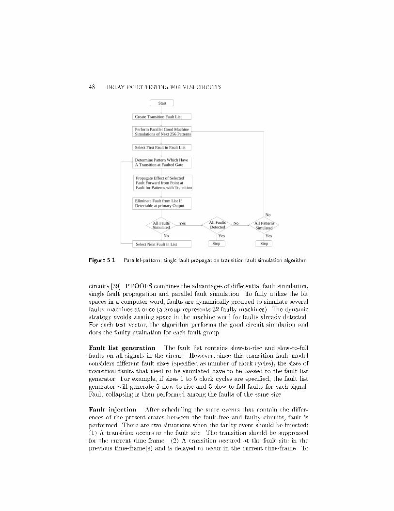
DELAY FAULT TESTING FOR VLSI CIRCUITS
Start
Create Transition Fault List
Perform Parallel Good MachineSimulations of Next 256 Patterns
Select First Fault in Fault List
Determine Pattern Which HaveA Transition at Faulted Gate
Propagate Effect of Selected Fault Forward from Point atFault for Patterns with Transition
Eliminate Fault from List If Detectable at primary Output
Simulated
Select Next Fault in List Stop
All Faults Detected
All Patterns Simulated
Stop
No
All Faults Yes
Yes
No
Yes
No
Figure Parallelpattern single fault propagation transition fault simulation algorithm
circuits PROOFS combines the advantages of dierential fault simulationsingle fault propagation and parallel fault simulation To fully utilize the bitspaces in a computer word faults are dynamically grouped to simulate severalfaulty machines at once a group represents faulty machines The dynamicstrategy avoids wasting space in the machine word for faults already detectedFor each test vector the algorithm performs the good circuit simulation anddoes the faulty evaluation for each fault group
Fault list generation The fault list contains slowtorise and slowtofallfaults on all signals in the circuit However since this transition fault modelconsiders dierent fault sizes specied as number of clock cycles the sizes oftransition faults that need to be simulated have to be passed to the fault listgenerator For example if sizes to clock cycles are specied the fault listgenerator will generate slowtorise and slowtofall faults for each signalFault collapsing is then performed among the faults of the same size
Fault injection After scheduling the state events that contain the dierences of the present states between the faultfree and faulty circuits fault isperformed There are two situations when the faulty event should be injected A transition occurs at the fault site The transition should be suppressedfor the current timeframe A transition occured at the fault site in theprevious timeframes and is delayed to occur in the current timeframe To

DELAY FAULT SIMULATION
Choose a fault from the fault group
present state
present state different from fault-free
Is faulty
Are there
fault groupmore faults in this
Are there
faultsany undetected
values at the fault siteUpdate the array of the previous
Store the difference of the faultystates from fault-free states
fault list more faults in the Are there
Are all
simulatedtest vectors
Start
Assign an unknown initial valueto all signals
Choose a group (32) of transitionfaults at a time
Yes
No
Yes
No
Yes
No
Schedule the events
Yes
No
No
Yes
Inject the fault
Simulate faulty events
Drop detected faults
Simulate fault-free circuit
Generate fault list
Stop
Figure Flowchart of the TFSIM algorithm
examine these conditions it is necessary to know the values of the faulty signal in previous timeframes If the size of the target transition fault is k clockcycles the values of the faulty signal in the previous k timeframes have to beknown These values are recorded and updated at the end of the simulation foreach vector At the beginning of the simulation for the rst vector the initialvalue of the faulty signal is assumed to be an unknown value UA traditional implementation of fault injection uses a ag for each gate The
ag indicates whether the associated gate is faulty or not This implementationrequires that the ags be examined for every gate evaluation even though onlyone gate is faulty The fault injection method proposed in does not requirethe use of special ags For each fault an extra gate is inserted into the circuitThe concept of inserting an extra gate for fault injection of stuckat faults has

DELAY FAULT TESTING FOR VLSI CIRCUITS
been given in To inject a slowtorise fault of size k clock cycles a k input AND gate is inserted at the faulty signal This is illustrated in Figure The values of the rst k inputs of the extra gate are set to the values of thefaulty signal in previous k timeframes Note that if the value of signal A is alogic in any of the previous k timeframes the value of signal B in the currenttimeframe will be a logic If the value of signal A is a logic in all previous ktimeframes the value of signal B in the current timeframe will be the currentvalue of signal A Similarly to inject a slowtofall fault of size k clock cyclesa k input OR gate is inserted at the faulty line and the values of rst kinputs to the extra gate are set to the values of the faulty signal at the previousk timeframes
An-k+1An-k
n-1A
A
B
n
n
(b) before insertion
An
(a) after insertion
Figure Fault injection at timeframe n for a slowtorise fault at signal A of size k
clock cycles
Example Consider the example given in Figure The values at signalB can be expressed in terms of the values at signal A as
Bn An An An
n-1AAn-2
An B n
Figure Fault injection example
Therefore the suggested fault injection technique produces a correct waveformat the fault site

DELAY FAULT SIMULATION
When simulating faulty circuits in paralell except for the injected faultthe values of the rst k inputs to the extra gate are set to a logic value if anAND gate is inserted and to a logic value if an OR gate is inserted
Storing states of faulty circuits At the end of each vector simulation inaddition to storing the dierence between the faulty state and the faultfreestate the value at the faulty signal the k th fanin of the inserted gateshould be also stored For each fault of size k clock cycles an array of size kis used to store the values of the faulty signal in the previous k timeframesThe arrays are updated for all undetected faults at the end of the simulationfor each vector These arrays are used for fault injection as described aboveThe TFSIM algorithm has very low memory requirements In addition to
the memory for storing the values of the faultfree circuit for all signals forone timeframe and the memory for storing the dierences between the faultfree and each undetected faulty circuit at the next state signals as used inPROOFS TFSIM requires an array of k bytes for each undetected faultof size k clock cycles to store the values of the faulty signal in the previous ktimeframes
Unknown initail value In TFSIM an unknown initial value U is assumedfor each signal Under this assumption a transition fault may prevent a circuitfrom fault initialization As an illustration consider transition faults of sizeone clock cycleIn threevalued logic there are nine possible combinations of the previous
value and current value at a signal U U U U and UU Ifthe valuepair at the fault site is a rising transition occurs and the slowtorise fault should be injected The current faulty value becomes If the valuepair is U U or UU a rising transition may or may not occur dependingon the powerup states of the ipops For example if the faulty valuepairis U before fault injection the slowtorise fault is injected and the currentfaulty value becomes U Similarly if the faulty valuepair is U before faultinjection the slowtorise fault is injected and the current faulty value becomes Table summarizes the actions of fault injections for all valuepairsIf teh valuepair of the faulty signal is U before injection the current value
of the signal becomes U after the slowtorise fault is injected Similarly if thevaluepair of the faulty signal is U the current value of the signal becomes Uafter the slowtofall fault is injected The following example illustrates thata transition fault may prevent the circuit from being initialized and thus it isuntestable while the corresponding stuckat fault is initializable and testable
Example Consider a threebit counter with a reset input The most significant bit is a primary output The input sequence is the reset vector followed bya sequence of clock pulses Table lists the states of the faultfree circuit thestates of the circuit with a slowtofall fault of size one clock cycle at the leastsignicant bit denoted LSB in the table and the states of the circuits with

DELAY FAULT TESTING FOR VLSI CIRCUITS
Valuepair at the faulty signalbefore injection after injection
slowtorise slowtofall
U U U UUU UU UU
No injection
Table Fault injection
stuckat and stuckat faults at the least signicant bit As it can be seenfrom the table neither a stuckat nor a stuckat fault prevents the circuitfrom initialization while the circuit with a slowtofall fault is not initializedand is undetected
input faultfree LSB slowtofall LSB stuckat LSB stuckatevent circuit
initial state UUU UUU UUU UUUreset U clock UU clock UUU ! clock UUU clock UUU !clock
clock
clock
clock
! Fault is detected
Table Faulty states for unknown initial values
However if we enumerate the two possible initial binary values and at thefault site and simulate them separately the problem is solved for this exampleTable lists the faulty states for dierent initial values The sequence detectsthe slowtofall fault for both cases at the same vector

DELAY FAULT SIMULATION
input faultfree LSB slowtofall LSB slowtofallevent circuit initial value initial value
initial state UUU UU UUreset clock clock clock ! !clock clock
clock
clock
clock
Fault is detected
Table Faulty states for dierent initial values
As illustrated the reported transition fault coverage may be too pessimisticif an unknown initial value is assumed for the faulty signal A higher faultcoverage can be achieved if each transition fault is treated as two faults onethat assumes an initial value at the faulty signal and the other that assumesan initial value of
GATE DELAY FAULT SIMULATION
PATH DELAY FAULT SIMULATION
Path delay fault simulation has been investigated by several research groups Smith proposes a sixvalued algebra forsimulating robust path delay faults in combinational circuits It consists of thefollowing values S S P P and Symbol S is used for signals withstable value during the application of a twovector input These signals do nothave any hazards The output of a gate is assigned value P if the transition onit cannot occur beforeall inputs with value P have changed from their initial values These signals
have a dierent initial and nal value but static or dynamic hazards might existbefore the signal stabilizes on its nal value Value is used for signals thatcannot be assigned neither value S nor value P These signals can have none oneor more transitions The sixvalued logic system is illustrated in Figure aThe implication tables for this system for AND OR and NOT gates are given inFigure b For each twovector test the simulation algorithm by Smith traces all undetected paths in the fault list and the paths with value P or Pon each signal in the path are marked as tested and removed from the faultlist The fault list contains all or selected paths in the circuit

DELAY FAULT TESTING FOR VLSI CIRCUITS
a
b
c a
bc a b
b a
S0
P0
-0
S1
P1
b a
S0 P0 -0 S1 P1 -1 a b
S0 S1
P0 P1
S1 S0
P1 P0
S0 P0 -0 S1 P1 -1
S0 S0 S0 S0 S0 S0
S0 P0 -0 S1 P1 -1
S0 -0 -0 P1 P1 P1
S0 -0 -0 P0 -0 -0
-1 S0 -0 -0 -1 P1 -1
P1 P1 -1 -1 S1 -1 -1
-1 -1 -1 -1 S1 -1 -1
S0 S0 P0 -0 S1 P1 -1
P0 P0 P0 P0 S1 -1 -1
-0 -0 P0 -0 S1 -1 -1 S0 -0 -0 -0 -0 -0
S1 S1 S1 S1 S1 S1 S1
-0 -1
-1 -0
-0
-1
S0
S1
P1
P0
(a)
(b)
Figure Implication tables for sixvalued logic
In nonscan sequential circuits the path delay fault simulation proceduredepends on the assumed test application scheme see Chapter If slowfastslow clock testing scheme is assumed the fault is activated only once duringthe application of the test sequence for that fault In atspeed scheme the faultcan be activated many times during the application of the test sequence Insequential circuits the path source can be a primary input or a ipop Thepath destination can be a primary output or a ipop Fault from the targetpath can aect some ipops other than the destination ipop Thereforethe fault simulators have to decide how to update the states of the ipopsother than the destination ipop after the activation of the target fault Forexample if during simulation a rising transition arrives to the destination ipop the correct value of the ipop will be If the rising transition arriveslate the destination ipop will latch in a value If a transition also reachessome ipops other than the destination ipop these ipops might latchin an incorrect value Chakraborty et al address path delay fault simulation for slowfastslow
and atspeed testing strategy in nonscan sequential circuits Two dierentfault models are considered In the rst model it is assumed that the faulteect reaches only the destination ipop All other ipops are assumed tolatch in their faultfree circuit values Tests generated for this fault model canbe invalidated by the presence of some faults other than the target fault In

DELAY FAULT SIMULATION
the second fault model only those ipops that have stable values withouthazards during fault activation are updated with their faultfree circuit valuesAll other ipops except the destination ipop are assigned an unknownvalue in the faulty circuit Tests generated for this fault model cannot beinvalidated However the fault coverage obtained with this fault model can bepessimistic
Bose et al also consider path delay fault simulation in nonscan sequentialcircuits Atspeed testing scheme is assumed The fault simulator is based onthe sixvalued logic system shown in Figure Both robust and nonrobustpath delay faults are simulated The only dierence in the implication table forAND gate for nonrobust path delay fault propagation is for the case a Pb for which the output c evaluates to P This is because it is assumedthat input b settles on its nal value quickly and the transition from inputa propagates to the output c Similarly for the OR gate case a P b evaluates to P For robust simulation the optimistic update rule is usedto update the values of the ipops after the fault activation According tothis rule all ipops with nonsteady values when the fault is activated areupdated with their faultfree circuit values given that they are destinations ofat least one robustly activated path Flipops with nonstable values that areresult of a nonrobust propagation are updated with an unknown value Flipops with steady values are assigned their faultfree values It can be proventhat faults found detectable using the optimistic update rule are guaranteed tocause a failure and cannot be masked by other faults in the circuit Thefault coverage using this rule is higher than if all the ipops with nonsteadyvalues are updated with an unknown value For nonrobust simulation all ipops other than the fault destination ipop are updated with their faultfreecircuit values
A variation of slowfastslow clocking strategy for simulation of nonscansequential circuits has been considered by Pomeranz et al For a testsequence consisting of k vectors all possible k schemes that have a singlefast clock are simulated in parallel only k schemes are considered since therst vector is needed for initializing the circuit In each of the k schemesthe fast clock is applied during a dierent test vector Also application ofmultiple fast clocks is considered Usually paths in the fault list are representedas a sequence of signals that belong to the path Once a path is detectedby a given test sequence it needs to be compared to the list of previouslydetected and stored path delay faults to nd the fault coverage This in turnrequires comparing sequences of signals To reduce the memory requirementsand increase the speed of the path delay fault simulation process paths canbe represented using path numbers Faults are then represented as pairspath number transition type where the transition type is rising or fallingBy assigning a unique path number for each path paths detected by the givenvector sequence can be found by comparing the path numbers rather thancomparing a sequence of signal numbers

DELAY FAULT TESTING FOR VLSI CIRCUITS
The number of path delay faults can be exponential in the number of linesin the circuit Therefore fault simulation methods that rely on enumeratingthe path delay faults both in the fault list and in the list of detected faultscannot process large number of faults The problem can be overcome by usingnonenumerative methods for estimating the path delay fault coverage Nonenumerative methods for combinational circuits have been proposed by several research groups Pomeranz et al propose a method that canestimate the fault coverage in time which is polynomial in the number of linesin the circuit The computed fault coverage is pessimistic in the sense that theexact fault coverage is never smaller than the estimated one The quality ofthe estimation can be improved by increasing the polynomial complexity of themethodThe total number of path delay faults can be found in linear time in the
number of lines in the circuit The procedure can be illustrated by thefollowing example
Example Consider the circuit in Figure To nd the number of pathsthe gates are processed in a topological order from primary outputs towardprimary inputs During processing all signals in the circuits are assigned integernumbers as follows Each primary output is assigned value Each inputto a gate is assigned the same value as the gates output The values on thefanout stems are obtained as a sum of the values on all of the fanout branchesFor example the value on the fanout stem f is obtained as a sum of the valueson the fanout branches f and f The value assigned to each signal in thecircuit is shown within square brackets The number of paths in the circuit canbe found as a sum of the values assigned to the primary inputs In our examplethe total number of paths is Then the number of pathdelay faults is twice the number of paths
c
d
g
j
[1]
[2]
[3][3]
a
h
l [1]
k [1][1]
[1]
[1][1]
[1]
[4]
[3]
f
e
b
[2]
[2]
[1]
[1]
2f
1f
Figure Counting the number of paths in a circuit
To nd the fault coverage we need to nd the number of detected path delayfaults with the given test The procedure for nding the number of path delayfaults robustly detected by a twoinput test pattern without enumerating thefaults is illustrated by the following example

DELAY FAULT SIMULATION
Example Consider the twovector test shown in Figure The valuesassigned under the test are shown inside the small squares next to each signalOnly primary inputs b c and e are assigned transitions under the test whileprimary inputs a and d are assigned stable denoted S and stable denotedS values respectively The list of signals in parentheses indicates the inputs tothe given gate that robustly propagate the transition to the gate output Onlysignals that are assigned transitions can have a list of signals associated withthem A list on a primary input contains the name of the primary input Forexample primary input b is assigned a falling transition and a list containingsignal b fbg The rising transition on signal f is due to the robustly propagatedtransition from input b Therefore signal f is assigned list fbg The transitionson signals e and f robustly propagate to signal i and the list on i is fe fgFinally the primary output k is assigned a transition that robustly propagatesfrom signal i and signal k is assigned list fig
a
b
S1
f
d
e
g
h
j
k
l
cg
e, f
cc
S0S1
e
bb i
Figure Counting the number of paths detected by a twoinput test
SEGMENT DELAY FAULT SIMULATION
Summary


TEST GENERATION FOR PATH
DELAY FAULTS
This chapter concentrate on value systems and methodologies proposed forgenerating tests for single and multiple path delay faults Robust nonrobustvalidatable nonrobust and functional sensitizable faults are considered as singlepath delay faults These paths usually can be tested with many dierent testsie there are many dierent robust tests for a robust testable path manydierent nonrobust tests for a nonrobust testable path etc Since robusttests are guranteed to detect a faulty target path independent on whether or notthere are delay faults on paths other than the target path most test generatorsdo dierentiate between robust tests for a given path These test generatorsdo not use any timing information On the other hand some nonrobust testshave a higher probability of detecting a faulty nonrobust testable path thanthe others Similar holds for functional senitizable tests This chapter presentstest generation algorithms that can produce high quality tests based on usingthe timing information of the circuit for nonrobust and functional sensitizablefaults A nonrobust test for a given target path becomes invalid if certainother paths in the circuit are defective If the faults that may invalidate thenonrobust test for the target path can be robustly tested these robust testsalong with the nonrobust test for the target path form a validatable nonrobusttest VNR An algorithm for automatic generation of validatable nonrobusttests is outlined in this chapter
Testing only single path delay faults is not sucient to gurantee the circuitperformance Some multiple delay faults multiple primitive faults can also

DELAY FAULT TESTING FOR VLSI CIRCUITS
aect the performance Identifying and testing such faults for large multileveldesigns is a hard task An algorithm that can identify and test double primitivefaults is presented
ROBUST TESTS
Process variations usually aect delay of more than one gate or interconnect inthe circuit Therefore it would be ideal if all path delay faults could be testedunder conditions that are independent of the delays on signals and gates outsidethe target path However this is possible only for a subset of path delay faultscalled robust testable faults Denition of robust testable path delay faults hasbeen given in Section Robust testable path delay faults have been rst considered by Smith
He suggested a sixvalued logic system to nd the path delay faults tested by agiven twovector pattern Test generation for robust path delay faults has beenrst addressed by Lin et al They propose a vevalued logic for generatingtests for robust testable paths The logic system consists of values fS S UU XXg These symbols represent the initial and nal values of a signal undervector pair V hv vi Symbol S S is used for signals for which the initialand nal value are Signals with S or S values are asssumed to behazardfree under vector pair V Symbol U U represents signals for whichthe nal value is The initial value can be or or there could be hazardson the signal before it settles on its nal value Symbol XX represents signals forwhich the initial and nal value are unspecied Figure illustrates thecovering relations in the proposed logic sytem Value U U covers S S
XX
U0 U1
S0 S1
Figure Covering relations in the vevalued logic system
while XX covers both U and U In this value system a transition can only berepresented using U for falling transition and U for rising transition Linet al use the convention that for the signals on the target path symbolsU and U can represent only a falling and rising transition respectively whilefor the signals outside the target path these symbols are intrepreted as denedearlier The implication tables for AND OR and NOT logic gates for thevevalued logic system are shown in Figure A twovector test V hv vi is a robust test for a given path delay fault
if it lauches the desired transition at the source of the path and if the valueson the paths oinputs have logic values that are covered by the values givenin Figure For example if the oninput to an AND or NAND gate is

TEST GENERATION FOR PATH DELAY FAULTS
a
bc
S0
U0
S1
U1
XX
S0 U0 S1 U1 XXb a
S0 U0 S1 U1 XX
U0 U0 S1 U1 XX
S1 S1 S1 S1 S1
U1 U1 S1 U1 U1
XX XX S1 U1 XX
a ba
b
c
S0
U0
S1
U1
XX
S0 U0 S1 U1 XX
S0 U0 U1 U1 XX
S0 U0 S1 U1 XX
S0 U0 U0 U0 U0
S0 S0 S0 S0 S0
S0 U0 XX XX XX
b a
a b
S0 S1
U0 U1
S1 S0
U1 U0
XX XX
Figure Implication tables for AND OR and NOT gates
assigned a rising transition the oinput can be assigned any value covered byU ie value S or U As it can be seen from the gure in the proposed
Rising
Falling
U1
S1
S0
U0
NAND NORAND OR
on-inputtransition
typegate
Figure Values covering the oinput values
vevalued logic system the values on the oinputs are uniquely determinedThey satisfy the conditions given by Denition for robust oinputsA PODEMtype test generation algorithm based on this logic system has
been proposed by Patil et al It starts with the list of paths for which testshave to be generated Next given the path and a transition at the source of thepath a list of signal values required for the oninputs and oinputs accordingto the table in Figure are generated Given this list the test generatorattempts to justify the signals in the list using a PODEMtype algorithm After a partially specied test is generated a heuristic procedure is used toconvert the unspecied XX or partially specied U or U values at primaryinputs into specic values such that the probability of detecting the remainingpath delay faults with the same test is maximizedTest generation algorithms for robust path delay faults have also been pro
posed by many other researchers For example Fuchs et al propose atenvalued logic system and a stepwise path sensitization procedure to generate robust tests This procedure is capable of handling a large number of pathdelay faults The experimental results on many benchmark and industrial designs have shown that usually only a small number of path delay faults can be

DELAY FAULT TESTING FOR VLSI CIRCUITS
tested by a robust test Saldanha et al propose a robust tests generationalgorithm that employs a singlestuck at fault test generator on a modiednetworkRecently it was shown that a twovector tests for robust path delay faults
might not always excite the worse case delay of the target path Theoinput transitions and preinitialization are shown to have signicant impacton the delay of the target path Chen et al propose a robust path delayfault test generator that incorporates these two additional considerations Itgenerates threevector robust tests that excite the worst case delay of the targetpath
HIGH QUALITY NONROBUST TESTS
Nonrobust testable paths have been dened in Section As it was showna nonrobust test becomes invalid if the transition on any nonrobust oinputarrives later than the transition on the corresponding oninput A nonrobusttestable path can usually be tested with many dierent nonrobust NR testsTest generation techniques for nonrobust testable path delay faults have beenproposed in literature However these techniques cannot make a distinction between dierent nonrobust tests for a given path Cheng et al show that some nonrobust tests have a higher quality than the others Theiralgorithm for generating high quality nonrobust tests is based on includingtiming information into the test derivation process A metric called robustnessis introduced to measure how far a given nonrobust NR test is from a robusttest Then for each nonrobust testable fault this metric is used to generate anonrobust test which is closer to a robust testThe following notation and denitions will be used in describing the algo
rithm for generating high quality nonrobust tests Let V hv vi be aninput vector pair applied for delay testing of a given target path and let v beapplied at time t At some time after t the logic values on the signalsin the circuit will become stable It is assumed that the signal delays in thefaultfree circuit are equal to the nominal signal delays
Definition The time when the logic value on signal f becomes stable underv is called arrival time of f under v The arrival time at signal f under vin the faultfree circuit is denoted with AT f v
Definition For a given oinput g and its corresponding oninput f thedierence AT f vAT g v is called slack of the oinput g
A nonrobust testable path under any test vector pair has at least one nonrobust oinput while the rest are robust oinputs see Section Thenumber of nonrobust oinputs for a given target path can be dierent fordierent nonrobust tests Since the goal of the algorithm is generating nonrobust tests that aremore robust its rst objective is to nd a test with minimalnumber of nonrobust oinputs for a given target path Also two nonrobust

TEST GENERATION FOR PATH DELAY FAULTS
(a)
16ns17ns
S1
S0
20ns
(b)
8nsS1
S0
S0
S17ns
S0
(c)
XX
5ns
20ns
X0
X0
X0
18ns
5ns
7ns6ns
5ns
6ns
20ns
X0
XXXX
Figure Dierent nonrobust tests can tolerate dierent timing variations
tests with the same number of nonrobust oinputs can have dierent qualitywith respect to their eectiveness in detecting defects Slack of the nonrobusttest is dened to help guide the test generation process towards generating highquality nonrobust tests
Definition Let g g gn denote the nonrobust oinputs for a giventarget path under a given vector pair V Let s s sn denote the slacks ofthose nonrobust oinputs Then the slack of the nonrobust test V isdened as min
infsig
The second objective of the algorithm is to nd the nonrobust test with themaximum slack among all nonrobust tests for a given path If the slack at thenonrobust oinputs is larger the probability that the nonrobust oinputtransition masks the oninput transition is lower In other words a nonrobusttest with a larger slack can tolerate larger timing variations at the nonrobustoinputs For delay defects caused by process variation the slack of a nonrobust test should be closely related to the probability of fault masking at thenonrobust oinputs
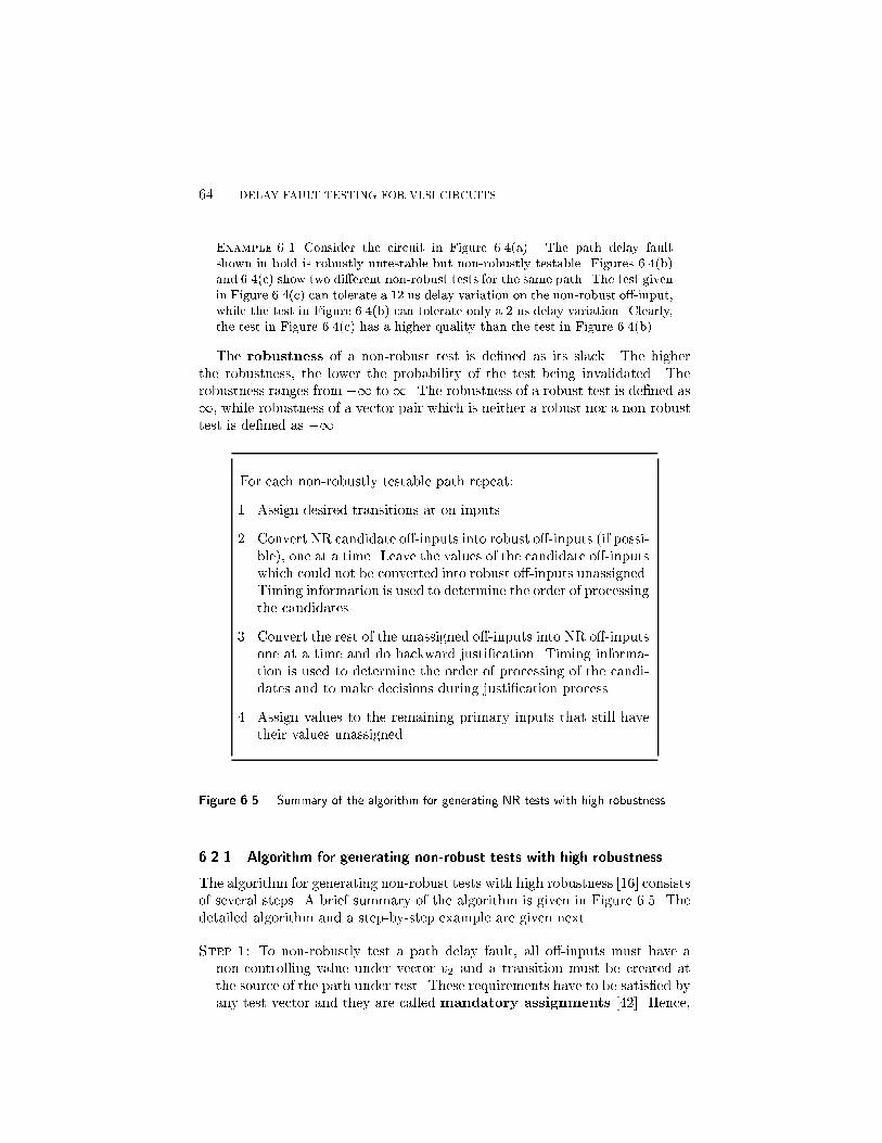
DELAY FAULT TESTING FOR VLSI CIRCUITS
Example Consider the circuit in Figure a The path delay faultshown in bold is robustly untestable but nonrobustly testable Figures band c show two dierent nonrobust tests for the same path The test givenin Figure c can tolerate a ns delay variation on the nonrobust oinputwhile the test in Figure b can tolerate only a ns delay variation Clearlythe test in Figure c has a higher quality than the test in Figure b
The robustness of a nonrobust test is dened as its slack The higherthe robustness the lower the probability of the test being invalidated Therobustness ranges from to The robustness of a robust test is dened as while robustness of a vector pair which is neither a robust nor a nonrobusttest is dened as
For each nonrobustly testable path repeat
Assign desired transitions at oninputs
Convert NR candidate oinputs into robust oinputs if possible one at a time Leave the values of the candidate oinputswhich could not be converted into robust oinputs unassignedTiming information is used to determine the order of processingthe candidates
Convert the rest of the unassigned oinputs into NR oinputsone at a time and do backward justication Timing information is used to determine the order of processing of the candidates and to make decisions during justication process
Assign values to the remaining primary inputs that still havetheir values unassigned
Figure Summary of the algorithm for generating NR tests with high robustness
Algorithm for generating nonrobust tests with high robustness
The algorithm for generating nonrobust tests with high robustness consistsof several steps A brief summary of the algorithm is given in Figure Thedetailed algorithm and a stepbystep example are given next
Step To nonrobustly test a path delay fault all oinputs must have anoncontrolling value under vector v and a transition must be created atthe source of the path under test These requirements have to be satised byany test vector and they are called mandatory assignments Hence

TEST GENERATION FOR PATH DELAY FAULTS
in the rst step all mandatory assignments and their implications arefound
Next the earliest arrival time of each signal restricted to these mandatoryassignments are computed Note that certain input vector pairs may producevalues that violate the given set of mandatory assignments SMA at somesignals The earliest arrival time at signal f under a given SMA isdened as the earliest arrival time at f among all vector pairs not violatingthe SMA
Example Consider the circuit in Figure a The target path isshown in bold The arrival times and the transitions for the signals on
5ns
21nsa
1X
1XXX
XX
XXc
X0X0
h
X1
1X
1X
X1 20ns8ns
b
f
e
g
j
(a)
(b)
d
i
k
a = 5ns
c = c = 0ns
d = 6ns
e = 1ns
f = 0ns
g = 7ns
h = 2ns
i = 8ns
j = j = 0ns
k = 1nsb = b = 0nsr f
r
f
f
f
f
f
f
f
r f
r
r
Figure Computing the SMA and the earliest arrival times
the target path are as shown Signals b c f and j are primary inputsand the transitions on them are assumed to arrive at time t Allgates are assumed to have a unit delay for both the rising and fallingtransition After assigning noncontrolling values under the second vectorv to all oinputs and after implying these values the obtained set ofmandatory assignments is as shown Next the earliest arrival times forall signals under the given SMA are computed These values are shownin Figure b Notation sf and sr is used to denote the arrival timesof the falling and rising transitions on signal s respectively For exampledf ns means that the earliest arrival time for a falling transition onsignal d under the given SMA is ns

DELAY FAULT TESTING FOR VLSI CIRCUITS
Definition For a nonrobust testable path the oinputs whose corresponding oninput has a ncvcv value are called NR candidate oinputs
Example In Figure a the oinputs f i and k are NR candidateoinputs
Step All NR candidate oinputs for the target path are identied and anattempt is made to convert them one at a time into robust oinputs byassigning a stable noncontrolling value to them To order the NR candidateoinputs for processing the slack of each NR candidate oinput ie thedierence between the arrival time of the corresponding oninput and theearliest arrival time of the transition on the NR candidate oinput is computed The NR candidate with the smallest slack is processed rst This isbecause a nonrobust oinput with a smaller slack has a higher probabilityof masking its oninput transition than a nonrobust oinput with a largervalue of slack
Example Consider again the circuit in Figure a The slacks ofNR candidate oinputs are slackf ns slacki ns and slackk ns Since the NR candidate oinput f has the smallest slack signalf is rst tried to be converted into a robust oinput by assigning a stable S value to it The assignment of S value to f and its implications donot cause any conicts and therefore signal f is successfully convertedinto a robust oinput
Next the signal earliest arrival times are incrementally updated This isneeded because for certain signals the signal earliest arrival times may changedue to the augmented set of mandatory assignments
Example In the circuit in Figure a the earliest arrival time ofsignal g is removed from the set since g has a stable value under thenew SMA and the earliest arrival time of signal i becomes if nsThe slacks of the NR candidate oinputs now are slacki ns andslackk ns Therefore the oinput i is selected as the next signalfor processing However under the given SMA it is not possible to assigna stable noncontrolling value to signal i and signal k is processed nextOinput k can be converted into a robust oinput by assigning a stable value to primary input j The new SMA and the signal earliest arrivaltimes are shown in Figure
Step For the NR candidate oinputs which cannot be converted into robust oinputs assigning nonrobust transitions cannot be avoided underthe current partially assigned test T To minimize the probability that theoninput transition is masked by the transition at a nonrobust oinput anattempt is made to nd a test for which the arrival time of the transition

TEST GENERATION FOR PATH DELAY FAULTS
i = 3nsa = 5ns
b = b = 0ns
c = c = 0ns
d = 6ns
e = 1ns
h = 2nsr
r f
r f
f
f
f
f
20ns8ns21ns
a
1X
1X
XXb
XXc
f
d
g
h
jk
X1
1X
S1
5nsS0
S0
e
S0i
(a)
(b)
Figure Converting nonrobust oinputs into robust oinputs
at the oinput is the earliest possible This can be achieved by using thecalculated earliest arrival times to guide the justication process To justifya transition at the output of a gate among all inputs that can have a transition under current partial test a transition is assigned to the input withthe earliest arrival time All other inputs to the gate are assigned stablenoncontrolling values This backward justication process continues untilthe primary inputs are reached or a conict has occurred In the latter casethe algorithm backtracks to the last decision point and justifes the transitionat the input with the next earliest arrival time The justication and backtracking process are very similar to those used in stuckat test generationalgorithms
In this test generation process the values at internal signals and primaryinputs are gradually assigned Therefore those NR candidate oinputswhich are processed later will have a smaller search space than those thatwere processed rst This is why the most critical NR candidate oinputsthe ones with the smallest slack rst are processed rst
Example Consider the circuit in Figure a Signal i is a NR oinput for the target path The objective is to make sure that the fallingtransition on signal i arrives as early as possible Since the value at signalh has to be justied using the calculated earliest arrival times for signalsd and e it can be seen that the transition on signal i will be the earliest

DELAY FAULT TESTING FOR VLSI CIRCUITS
20ns
5ns
8ns21ns
a
c
f
d
j
X1
S1S0
S1
S1
S1
S0
e
bi S0
k
h
g
S0
Figure Backward justication and assigning unspecied values at PIs
if a falling transition is assigned to signal e and stable to signal d Thisis illustrated in Figure
Step Finally to obtain a completely specied test and to minimize thenumber of sensitized paths associated with the nonrobust oinputs it isnecessary to check if there are some primary inputs that do not have valuesassigned and they are assigned such that the number of transitions at theprimary inputs is minimized ie value X is specied as X is speciedas and XX as or Test compaction is not considered in this workIf test compaction is used this step of the algorithm can be omitted
Example The only primary input that does not have values completely specied is input c and in this step it is assigned a stable valueThe nal values on all signals are shown in Fig
VALIDATABLE NONROBUST TESTS
Validatable nonrobust path delay faults have been dened in Section The validatable nonrobust tests guarantee to detect a fault and thereforeshould be used for nonrobustly testable paths whenever they existThere may exist many validatable nonrobust tests for a given fault To
reduce the test set size it is of interest to nd a test such that the number ofpaths that have to be robustly tested to validate the nonrobust test for thetarget path is minimal An algorithm for automatic generation of such a set oftwopattern tests is proposed in It consists of several steps
Step For each nonrobust testable fault the NR candidate oinputs dened in Section are converted into robust oinputs and a nonrobust
TEST GENERATION FOR PATH DELAY FAULTS
test with a minimal number of nonrobust oinputs is obtained This isdone using the procedure described in Section After processing all NRcandidate oinputs a partially specied nonrobust test is obtained
Step The unspecied values at the primary inputs are specied such thatthe number of transitions at the primary inputs is minimized The nalnonrobust test is denoted as T Next the implications of T are performed
Step The nonrobust oinputs are examined and the paths that need tobe robustly tested to validate T are identied see Figure
In developing test T the number of transitions at primary inputs is minimized Therefore typically only a very small number of partial paths thatend at a nonrobust oinput is sensitized Thus in Step only a small number of paths need to be examined This not only reduces the computationalcomplexity but it also reduces the cardinality of the validatable nonrobust testThere is a possible extension of this algorithm for identifying more VNR
testable paths The condition for robustly testing the sensitized partial pathsfrom primary inputs to nonrobust oinputs can be relaxed so that they aretested under the VNR condition However if this extension is adopted thefollowing situation may occur in generating a VNR test for path A the VNRtestability of path B is required and in generating a VNR test for path B theVNR testability of path A is required In this case neither of the paths is VNRtestableAs Cheng et al show including the timing information into the process
of nonrobust test generation can substantially improve the quality of a nonrobust test However experimental results on a large set of benchmark andindustrial designs show that typically only a small number of paths in thecircuit can be tested under nonrobust and validatable nonrobust criteria On the other hand most circuits have a large number of functional sensitizablefaults These faults under can certain conditions aect the performance of thedesign Therefore to further improve of the quality of delay tests it is necesaryto derive tests for functional sensitizable paths
HIGH QUALITY FUNCTIONAL SENSITIZABLE TESTS
Functional sensitizable path delay faults have been dened in Section Toguarantee that a given functional sensitizable FS path delay fault will notaect the performance of the circuit a set of functional sensitizable tests hasto be applied These tests will be considered in Section In this section thegoal is to generate a small number of tests eg one for a given FS path suchthat they are most likely to detect the faultDierent functional sensitizable tests have a dierent probability of detecting
a defect on an FS path

DELAY FAULT TESTING FOR VLSI CIRCUITS
(a)
(b)
0ns
1ns
8ns
9ns
S0
20ns
5ns
1T :
2T :
PO
PO
0ns
1ns
8ns
9ns
S0
15ns
g
20ns
f
Figure Dierent quality functional sensitizable tests
Example Consider the functional sensitizable test T shown in Figure aThe target path is shown in bold and signal g is a functional sensitizable oinput under test T Under this test in the faultfree circuit the rising transitionat oinput g arrives at ns while the rising transition on the oninput f arrives at ns The arrival time of the transition at the primary output will bedetermined by the earlier arriving signal between signals f and g This meansthat if in a faulty circuit the transition at the oinput g arrives more than nslate the fault on the target path will propagate to the primary output Otherwise the fault on the target path will not be detectable with test T Nextconsider the functional sensitizable test T for the same target path shown inFigure b Signal g is again a functional sensitizable oinput Howeverunder test T in the faultfree circuit the transition at signal g arrives at nsTherefore in the faulty circuit the rising transition on the oinput g needs tobe more than ns late to observe the fault on the target path
If one to can aord selecting only a small number of input vector pairs to testa functional sensitizable path one should select those tests that have a higherprobability of making the defects on the FS path observable In the aboveexample test T is better than test T since it requires smaller delay faults onsignals outside the target path to detect a defect on the target path Thereforefor a good FS test the nominal arrival times of the FS oinputs should be aslate as possible ie the slack of the FS oinput should be as small as possibleAn algorithm for generating high quality functional tests is given in andit will be reviewed in this section The algorithm is based on using the circuittiming information to derive high quality FS tests For each tested FS pathonly one FS test is derivedA necessary condition to detect a defective functional sensitizable path with
a given test is that the transitions on the FS oinputs arrive later than the

TEST GENERATION FOR PATH DELAY FAULTS
transitions on the oninputs Hence in general if the number of FS oinputs islarger the probability of detecting a defect is smaller The number of functionalsensitizable oinputs in a given path depends on the applied test vector pairTherefore one of the goals of the algorithm in is to minimize the numberof FS oinputs Reduction of the number of FS oinputs can be achieved bymaximizing the number of oinputs that are robust or nonrobust Howevertwo FS tests with the same number of FS oinputs can still have a dierentquality as the above example shows
Definition Let g g gn denote the FS oinputs under a given vectorpair V and let s s sn denote the slacks of those FS oinputs Then theslack of the FS test V is dened as max
infsig
The second goal of the test generation algorithm is to nd tests whose valueof the slack is minimal The slack in this case can be positive or negativeThe algorithm searches for a test with the most negative slack if it existsOtherwise it looks for one with the least positive slack Such tests can tolerateonly small timing variations on their FS oinputs and are more likely to leadto the detection of a faulty FS path
Algorithm for generating functional sensitizable tests The set of FSpaths that need to be tested can be identied using any of the algorithmsdescribed in Section In the process of generating nonrobust tests the oinputs whose corresponding oninput has a ncvcv transition were called NRcandidate oinputs Here in the context of generating tests for FS paths suchoinputs are redened as FS candidate oinputs
Definition The oinputs whose corresponding oninput has a ncvcv
transition are called FS candidate oinputs
The algorithm for generating high quality functional sensitizable tests for agiven FS path consists of several steps
Step Find the FS candidate oinputs
Step Depending on the transitions assigned under the given test vector anFS candidate oinput can become either robust nonrobust or functionalsensitizable oinput The goal is to minimize the number of FS oinputsThus an attempt is made to generate a test under which the highest numberof FS candidate oinputs is either robust or nonrobust Because the transition on a nonrobust oinput can mask the transition on the correspondingoninput while this can never happen in the case of a robust oinput itis preferred to have as large number of robust oinputs as possible TheFS oinput candidates are processed one at a time For each candidatethe rst attempt is to convert it into a robust oinput by assigning a stable noncontrolling value to it Similar to the algorithm in Section theforward implication and backward justication process are used to check if

DELAY FAULT TESTING FOR VLSI CIRCUITS
the desired transition can be assigned If the attempt to convert some FScandidate oinput into robust oinput fails its value is left unspecied andthe algorithm proceeds with the next candidate in the list
Step After all FS oinput candidates have been processed the algorithmstarts over with the ones that have their values still unspecied and tries toconvert them into nonrobust oinputs by assigning a cvncv transition tothem
Step If the attempt to convert some FS candidate oinput into nonrobustoinput fails a ncvcv transition is assigned to it ie it is converted intoan FS oinput
The order of processing the FS candidate oinputs is very important forgenerating good quality FS tests Therefore the algorithm uses the partialtiming information available under the current set of mandatory assignmentsand their implications to calculate the earliest arrival time of the transitionon each of the FS candidate oinputs This information is then used forcalculating the slack of each candidate The candidates with the larger slackare processed rst since they are less likely to allow the propagation of thedefect to the primary output see example in Figure Therefore it isdesired that they be converted into robust or nonrobust oinputs The FScandidate oinputs that have a smaller slack have a higher chance of sensitizing the given FS path under faulty conditions and they can be convertedinto FS oinputs Each time after some FS candidate oinput has successfully been assigned a transition the set of mandatory assignments and theirimplications are updated and the slacks of the FS oinput candidates arerecompured
Step After the appropriate transitions have been assigned to all FS candidate oinputs the nal justication process is done in a way which maximizes the chance that the nonrobust oinputs arrive as early as possiblewhile the FS oinputs arrive as late as possible If the target path hasboth nonrobust and FS oinputs and if the fanin cones of some nonrobust and FS oinputs intersect the justication process is done so thatthe nonrobust oinput arrives as early as possible
To generate tests under which the FS oinputs arrive as late as possible thefanins to a gate whose output needs to be justied are sorted such that thelatest arriving signal is the rst in the list If the transition that needs to bejustied is cvncv an attempt is made to assign this transition to all faninsthat could have a transition under the current partially assigned vector pairprocessing them as they appear in the fanin list If the transition that needsto be justied is ncvcv the algorithm tries to assign this transition tothe fanin with the latest arrival time among all the fanins that could havea transition under the partially assigned test and a stable noncontrollingvalue to the rest of the inputs If there is a conict in this justicationprocess the algorithm backtracks to the last decision point and attempts
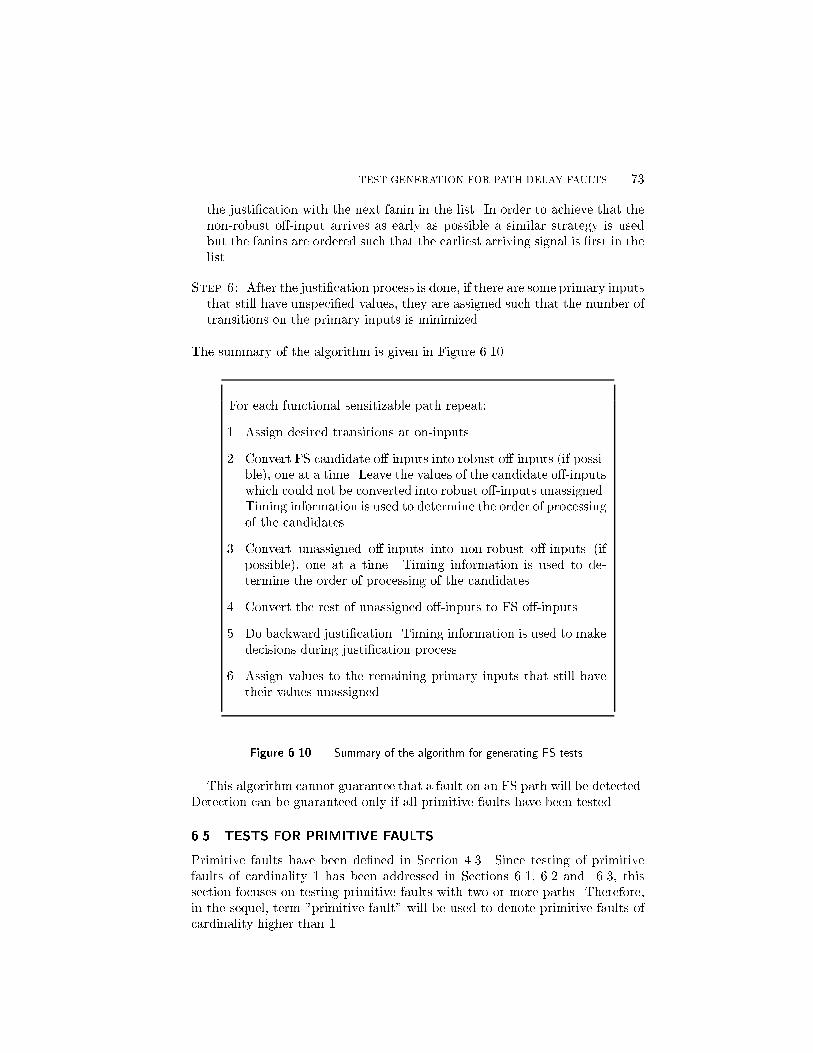
TEST GENERATION FOR PATH DELAY FAULTS
the justication with the next fanin in the list In order to achieve that thenonrobust oinput arrives as early as possible a similar strategy is usedbut the fanins are ordered such that the earliest arriving signal is rst in thelist
Step After the justication process is done if there are some primary inputsthat still have unspecied values they are assigned such that the number oftransitions on the primary inputs is minimized
The summary of the algorithm is given in Figure
For each functional sensitizable path repeat
Assign desired transitions at oninputs
Convert FS candidate oinputs into robust oinputs if possible one at a time Leave the values of the candidate oinputswhich could not be converted into robust oinputs unassignedTiming information is used to determine the order of processingof the candidates
Convert unassigned oinputs into nonrobust oinputs ifpossible one at a time Timing information is used to determine the order of processing of the candidates
Convert the rest of unassigned oinputs to FS oinputs
Do backward justication Timing information is used to makedecisions during justication process
Assign values to the remaining primary inputs that still havetheir values unassigned
Figure Summary of the algorithm for generating FS tests
This algorithm cannot guarantee that a fault on an FS path will be detectedDetection can be guaranteed only if all primitive faults have been tested
TESTS FOR PRIMITIVE FAULTS
Primitive faults have been dened in Section Since testing of primitivefaults of cardinality has been addressed in Sections and thissection focuses on testing primitive faults with two or more paths Thereforein the sequel term primitive fault will be used to denote primitive faults ofcardinality higher than

DELAY FAULT TESTING FOR VLSI CIRCUITS
Testing primitive faults was rst addressed by Ke and Menon Theypropose a technique for synthesizing a twolevel circuit such that all path delayfaults in the circuit are primitive Since representing a circuit in twolevel formmay not be practical they use algebraic transformations to convert a twolevelcircuit into a multilevel circuit while preserving its testability The test set generated for the twolevel circuit can also detect all primitive faults in the multilevel circuit The problem with this approach is that multilevel circuits obtained using only algebraic transformations are not areaecient and synthesistools usually use various Boolean transformations for areaperformancepoweroptimization
A method for identifying and testing primitive faults in multilevel circuitswas rst reported by Krstic et al It will be reviewed in this section Another method for testing primitive faults in multilevel circuits was presentedby Sivaraman et al This technique identies primitive faults by identifying sets of paths which determine the signal stabilization time at the circuitoutputs To be able to handle medium sized benchmark circuits iterative approach is proposed such that nding primitive faults of cardinality n requiresprevious identication of all primitive faults of cardinality n For largercircuits due to memory constraints only low cardinality up to primitivefaults are possible to be identied
All individual paths in primitive faults of cardinality higher than are functional sensitizable paths The methodology proposed by Krstic et al identies primitive faults by considering individual FS paths and by identifying allprimitive faults that the given FS path is involved in The algorithm is basedon the observation that single path delay faults contained in a primitive faulthave to merge at one or more gates to form a multiple path delay fault and suchgates can be quickly identied The technique can be combined with timinganalysis or any other method for selecting functional sensitizable paths thatneed to be tested see Section The following notation and denitions will be used in the description of the
algorithm for identifying and testing primitive faults For a given signal s twokinds of FS paths terminating at the same primary output can be dened FS paths for which the signal s assumes a a controlling value under vectorv cvFS paths through s and FS paths for which signal s assumesa noncontrolling value under vector v ncvFS paths through s Forsimplicity reasons the main ideas of the proposed methodology are explainedassuming that the circuit contains only input gates Extension to circuitscontaining gates with arbitrary number of inputs is straightforward Multipleoutput circuits are handled by processing each primary output and its fanincone separately
Cosensitizing gates
Cosensitizing gates with respect to a primary output A primitivefault must have at least one merging gate If one identies gates that can neverbe the merging gates for any primitive fault then one can signicantly reduce

TEST GENERATION FOR PATH DELAY FAULTS
the eort required to identify and test primitive faults This is especially trueif the number of nonmerging gates represents a signicant fraction of the totalnumber of gates in the circuit Gates that could possibly be the merging gatesin some primitive fault are called cosensitizing gates Gates on which nomerging of FS paths to form a primitive fault is possible are called noncosensitizing gates As it will be shown later identication of cosensitizinggates is easier than identication of merging gates
Definition A input gate g is a cosensitizing gate if every input to thegate has at least one cvFS path passing through it
If a gate has more than two inputs then the gate is a cosensitizing gate if ithas at least two inputs with nonzero number of cvFS paths passing throughthem If an input to some gate has no cvFS paths passing through it then allpaths passing through this input with a controlling value under vector v areeither robust nonrobust or functional redundant Therefore this input cannotbe part of any path in a primitive fault For example consider the circuit inFigure There are six functional sensitizable paths P ffalling aceghigP ffalling dghig P ffalling acfhig P frising acfhig P frisingbcfhig and P ffalling bceghig The circled numbers adjacent to each signalshow the number of cvFS paths through that signal Gates f h and i have just
2
12
0
1
2
0
15
0i
ab
cd
f
g
h
e
Figure Cosensitizing gates for a given PO
one input with cvFS paths and they cannot be cosensitizing gates The onlycosensitizing gates are c and g If a circuit has multiple outputs then a gatecan be a cosensitizing gate with respect to one PO and a noncosensitizinggate with respect to another PO
Cosensitizing gates with respect to an FS path Condition given byDenition identies the cosensitizing gates for any FS path in the fanincone of a given primary output To nd the primitive faults that a given FSpath is involved in the information about cosensitizing gates can be furtherrened In this renement process some of the cosensitizing gates with respectto a given PO might become noncosensitizing with respect to the target pathHowever all noncosensitizing gates with respect to the given PO will stay noncosensitizing with respect to any target FS path ending at that PO Severalrenement conditions are illustrated through examples

DELAY FAULT TESTING FOR VLSI CIRCUITS
oX1
X0g
P
X1
X1
X1
f
(b)
i
ab
cd
f
g
h
e
X1
(a)
Figure Cosensitizing gates for a given FS path
Example In the circuit in Figure a gate c is a cosensitizing gatewith respect to the primary output i Let the FS path for which the primitivefaults need to be found be P frising acfhig For a gate to be a cosenstitizinggate with respct to a given path the oninput and the oinput must be assigneda noncontrolling value under vector v Since under the set of mandatoryassignments SMA for P in Figure a the transition on input a does nothave a controlling value under vector v gate c cannot be a cosensitizing gatefor path P
Example Assume that the logic in Figure b is a part of some largercircuit Let path P be the target FS path and let gates g and f be the cosensitizing gates with respect to the primary output o The signal values shownin Figure b belong to the SMA for path P Since gate g is the last cosensitizing gate in P closest to the primary output no gate outside the fanincone of gate g can be a cosensitizing gate for path P Therefore gate f cannotbe a cosensitizing gate for path P
Example Also since under the SMA for P all oinputs to gate g are assigned a noncontrolling value under vector v gate g cannot be a cosensitizinggate for path P

TEST GENERATION FOR PATH DELAY FAULTS
Merging gates
There are several reasons why a cosensitizing gate may not be a merginggate First computing the exact number of cvFS paths through each signal inthe circuit can be prohibitively expensive since it requires consideration of twovectors v and v Approximate values for the number of cvFS paths througheach signal can be eciently computed by using only the information about thesecond vector v see Section However these numbers are pessimistic inthe sense that a functional redundant path may be counted as an FS pathOn the other hand FS paths can never be misclassied Second even if thecvFS path count can be computed exactly the information about the numberof cvFS paths passing through the inputs to a cosensitizing gate does not takeinto account any correlations between these paths Correlations between theFS paths can be twofold correlations manifested by a cosensitizing gate forwhich the cvFS paths cannot pass through together under any input vectorpair and correlations manifested by a cosensitizing gate for which a multipledelay fault involving only FS paths exists but it is a superset of some primitivefault One simple way to account for some of the correlations between the pathspassing through a given cosensitizing gate is to assign ncvcv transition toboth of its inputs and to nd the forward and backward implications of thisassignment If a conict is detected then the gate is not a cosensitizing gate
Identifying FS paths not involved in any primitive fault
As discussed in Section not all path delay faults need to be selected fortesting If all robustly and nonrobustly testable path delay faults are selectedthen some FS paths do not have to be selected In addition to the techniques foridentifying the set of FS paths that need to be tested described in Section the information about cosensitizing gates can be used to perform the selectionIf an FS path under the SMA does not have any cosensitizing gate then thepath does not have to be tested
Example Consider again the circuit in Figure a Gates c and g arecosensitizing gates with respect to the primary output The SMA and theirimplications for the functional sensitizable path P frising acfhig are asshown As discussed earlier gate c is not a cosensitizing gate for path PTherefore P has no cosensitizing gates and does not have to be tested Thefault on the target path can be observed only if paths ffalling dfhig and frisingbig are also faulty However both of these paths are robustly testable and ifany of them is faulty the robust test set will detect the fault Similarly itcan be determined that path P frising bcfhig does not have cosensitizinggates and it does not have to be tested Information about FS paths that donot require testing can be used to update the number of cvFS paths througheach signal For example paths P and P pass through signals c and h witha controlling value but these paths do not have to be tested Therefore thenumber of cvFS paths through signals c and h reduces by The updatedvalues for cvFS paths for our example circuit are shown in Figure

DELAY FAULT TESTING FOR VLSI CIRCUITS
2
10
1
2
0
1
0
0
i
ab
cd
f
g
h
e
3
Figure Updating the number of cvFS paths
This process of eliminating FS paths that do not have cosensitizing gates andupdating the number of cvFS paths through each signal can be repeated forseveral iterations Updating the values for cvFS paths results in a smallernumber of cosensitizing gates and a smaller number of FS paths that haveto be tested and helps reducing the test generation eort for primitive faultsHowever note that there exist FS paths that do not have to be tested butcannot be identied by examining only the number of cosensitizing gates Thisis because not every cosensitizing gate is a merging gate
Example Consider the FS path P ffalling acfhig in the circuit inFigure It has one cosensitizing gate gate c but it can be cosensitizedwith a robust path ffalling bcfhig and therefore does not need to be tested
Primitive faults of cardinality
A given FS path can participate in many primitive faults The cardinality k
of these primitive faults can be anywhere from up to the total number ofFS paths terminating at the given PO To guarantee that a fault on an FSpath will not aect the performance of the circuit all primitive faults thatinvolve the FS path have to be identied and tested The probability thatk long functional sensitizable paths will simultaneously be aected by defectssignicantly reduces as k increases Therefore identication and testing ofprimitive faults of low cardinality is of the highest signicance The followingalgorithm focuses on primitive faults of cardinality
Algorithm for identifying primitive faults of cardinality The algorithm for identifying and testing primitive faults of cardinality consists of twoparts First the cosensitizing gates and FS paths that need to be testedare identied This part of the algorithm involves several steps
Step The cosensitizing gates with respect to the given PO are identiedThis requires knowledge about the number of FS paths passing througheach signal This number can be found using the technique described inSection It gives the upper bound on the number of cvFS and ncvFSpaths through each signal Therefore the number of cosensitizing gates weidentify is also an upper bound
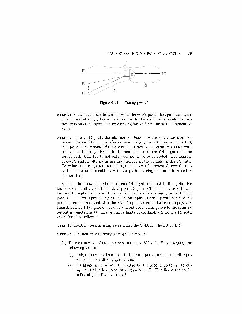
TEST GENERATION FOR PATH DELAY FAULTS
PI
PI
PO
Q
PI
P
R
gn
m
Figure Testing path P
Step Some of the correlations between the cvFS paths that pass through agiven cosensitizing gate can be accounted for by assigning a ncvcv transition to both of its inputs and by checking for conicts during the implicationprocess
Step For each FS path the information about cosensitizing gates is furtherrened Since Step identies cosensitizing gates with respect to a POit is possible that some of these gates may not be cosensitizing gates withrespect to the target FS path If there are no cosensitizing gates on thetarget path then the target path does not have to be tested The numberof cvFS and ncvFS paths are updated for all the signals on the FS pathTo reduce the test generation eort this step can be repeated several timesand it can also be combined with the path ordering heuristic described inSection
Second the knowledge about cosensitizing gates is used to nd primitivefaults of cardinality that include a given FS path Circuit in Figure willbe used to explain the algorithm Gate g is a cosensitizing gate for the FSpath P The oinput n of g is an FS oinput Partial paths R representpossible paths associated with the FS oinput n paths that can propagate atransition from PI to gate g The partial path of P from gate g to the primaryoutput is denoted as Q The primitive faults of cardinality for the FS pathP are found as follows
Step Identify cosensitizing gates under the SMA for the FS path P
Step For each cosensitizing gate g in P repeat
a Derive a new set of mandatory assignments SMA for P by assigning thefollowing values
i assign a ncvcv transition to the oninput m and to the oinputn of the cosensitizing gate g and
ii ii assign a noncontrolling value for the second vector v to oinputs of all other cosensitizing gates in P This limits the cardinality of primitive faults to

DELAY FAULT TESTING FOR VLSI CIRCUITS
b If SMA is not consistent go to Step Else if SMA is consistentexplore partial paths R from the oinput n to any PI in order to nda cosensitizing path that together with P forms a primitive fault ofcardinality The partial path R must be statically sensitizable underSMA and it also must be contained in some FS path The strategydescribed in Section can be used to quickly identify signals in theinput cone of signal n for which under the current SMA no staticsensitizable path can pass through Also in this step the informationabout the number of cvFS and ncvFS paths passing through each signalcan be used to prune the search for the partial path Once a partial pathR to PI is found it is necessary to check if the path cosensitized with Pat gate g is functional sensitizable If yes a primitive fault of cardinality is found If the path obtained by concatenation of path R and path Qis an FS path and partial path R is not static sensitizable under SMA itmeans that path P might be involved in a primitive fault of cardinalityhigher than If this is the case we proceed by exploring a dierentpartial path R The process continues until all statically sensitizablepartial paths from n to any PI are found
The owchart of the algorithm is shown in Figure Next the secondpart of the algorithm is illustrated with an example
Example Consider the circuit in Figure The circled numbers inFigure a show the number of cvFS paths passing through the given signal while the numbers inside the boxes show the number of ncvFS paths Thevalues are shown only for those signals for which the number of cv or ncvFSpaths is nonzero Gates i o and v are the cosensitizing gates with respect tothe primary output w Let the target path P for which all primitive faults ofcardinality need to be found be frising afnqruvwg This path is shown inbold in Figure b The SMA for P is also shown in the gure ignore fornow the values shown inside the boxes since they are not part of the SMA for P The only cosensitizing gate on P is gate v Therefore to nd a cosensitizedpath which together with path P forms a primitive fault of cardinality onlypartial paths associated with oinput t have to be explored Note that if theinformation about cosensitizing gates had not been used all partial paths associated with oinputs i m and t potential FS oinputs in the target pathwould have to been explored Next a noncontrolling value is assigned for thesecond vector v to all oinputs other than oinput t and a ncvcv transitionto oinput t These values are shown within small boxes in Figure bThen the partial paths from signal t to any primary input are examined Thepartial path associated with oinput t must be static sensitizable under thecurrent SMA Since the path cosensitized with P has to be functional sensitizable the search eort can be reduced by using the information about thenumber of cvFS and ncvFS paths passing through each signal For examplethere are no ncvFS paths through input m of gate p Figure a and gatep in Figure b assumes value for vector v Therefore all partial pathspassing through signal m can be eliminated from further consideration On the

TEST GENERATION FOR PATH DELAY FAULTS
Identify co-sensitizing gates in
Are there unprocessed
conflictsAre there any signal value
yes
yes
Found a primitive fault of cardinality 2
Are there more partial paths to be explored
yes
Doneno
no
no
FS path
co-sensitizing gates in
g
m
to all other off-inputs in path P
noff-input to PIs
assign a ncv->cv transition to
v 2
Explore partial paths from R
P
yes
on-input and off-input
Part 1
Part 2
Identify co-sensitizing gates
Refine the information about co-sensitizing gates by considering correlations between FS paths and by
with respect to a given PO
identifying FS paths that do not need to be tested
paths that need testingAre there unprocessed FS
For co-sensitizing gate in : P
P
n,assign ncv value for vector
tizable and is an FS pathR+Q
Is partial path static sensi- R no
no
yes
Figure Flowchart of the algorithm for identifying and testing primitive faults of
cardinality
other hand input i to gate p has ncvFS paths passing through it and thealgorithm has to continue checking all paths passing through signal i Oncea partial path is identied it is necessary to check if the path cosensitizedwith P is functional sensitizable In the example there are two primitive faultsof cardinality containing path P The rst primitive fault includes path P
and frising diptvwg The second primitive fault includes paths P and frisingeiptvwg

DELAY FAULT TESTING FOR VLSI CIRCUITS
1
1
11
1
2
3
3
1
2
2
3
5
(a)
(b)
f
i
j
k
lm
n
o
r
s
t
u
a
b
c
de
g
h
q
wv
X0
X0
X0p
f
i
j
k
lm
n
o
p
r
s
t
u
a
b
c
de
g
h
q
wv
X1X1
X1
X1
Figure Testing primitive faults of cardinality
Summary
Experimental results show that test sets generated under robust testabilitycriteria cannot detect all timing defects A defect on a nonrobust target pathwill not be detected if the transitions on certain signals outside the target patharrive late Among all possible NR tests for a nonrobustly testable path someNR tests are better than others in detecting delay defects A good NR testcan tolerate larger timing variations and its probability of being invalidated issmaller Generating such tests requires the use of circuit timing informationGenerating tests for robust and nonrobust path delay faults is not sucient
to cover all possible delay defects Functional sensitizable paths can undercertain conditions be responsible for the circuits performance degradationDefects on these paths can be detected only if multiple delay faults existIgnoring these multiple path delay faults called primitive faults in the pro
cess of test generation can lead to a poor delay test quality It is very dicult to

TEST GENERATION FOR PATH DELAY FAULTS
identify and test all primitive faults in multilevel circuits The existing techniques can eciently deal only with primitive faults that consists of a smallnumber of single paths


DESIGN FOR DELAY FAULT
TESTABILITY
ROBUST DELAY FAULT TESTABILITY
DESIGN FOR PRIMITIVE DELAY FAULT TESTABILITY
Summary


SYNTHESIS FOR DELAY FAULT
TESTABILITY
SYNTHESIS FOR ROBUST DELAY FAULT TESTABILITY
SYNTHESIS FOR PRIMITIVE DELAY FAULT TESTABILITY
Summary


CONCLUSIONS AND FUTURE
WORK


References
L Ackner and M R Barber Frequency Enhancement of Digital VLSITest Systems Proceedings of IEEE International Test Conference pages October
P Agrawal V D Agrawal and S C Seth Generating Tests for DelayFaults in Nonscan Circuits IEEE Design Test of Computers pages March
V D Agrawal and T J Chakraborty HighPerformance Circuit Testingwith SlowSpeed Testers Proceedings of IEEE International Test Conference pages October
V D Agrawal CJ Lin P W Rutkowski S Wu and Y Zorian BuiltInSelfTest for Digital Integrated Circuits ATT Technical Journal March
K A Bartlett et al Multilevel Logic Minimizing Using Implicit DontCares IEEE Transactions on ComputerAided Design of Integrated Circuits and Systems June
S Barton Characterization of HighSpeed Above MHz Devices usingAdvanced ATE Technique Results and Device Problems Proceedings ofIEEE International Test Conference pages October
S Bose P Agrawal and V D Agrawal Path Delay Fault Simulation ofSequential Circuits IEEE Transactions on VLSI Systems December
O Bula J Moser J Trinko M Weissman and Woytowich Gross Delay Defect Evaluation for A CMOS Logic Design System Product IBMJournal of Research and Development MarchMay
J L Carter V S Iyengar and B K Rosen Ecient Test CoverageDetermination for Delay Faults Proceedings of IEEE International TestConference pages September

DELAY FAULT TESTING FOR VLSI CIRCUITS
T J Chakraborty V D Agrawal and M L Bushnell Path Delay FaultSimulation Algorithms for Sequential Circuits Proceedings of First AsianTest Symposium pages November
T J Chakraborty V D Agrawal and M L Bushnell Delay Fault Modelsand Test Generation of Random Logic Sequential Ciruits Proceedings ofth Design Automation Conference pages June
LC Chen S K Gupta and M A Breuer High Quality Robust Testsfor Path Delay Faults Proceedings of th IEEE VLSI Test Symposiumpages May
KT Cheng Transition Fault Testing for Sequential Circuits IEEETransactions on ComputerAided Design of Integrated Circuits and Systems December
KT Cheng and HC Chen Classication and Identication of Nonrobust Untestable Path Delay Faults IEEE Transactions on ComputerAided Design of Integrated Circuits and Systems August
KT Cheng S Devadas and K Keutzer DelayFault Test Generationand Synthesis for Testability Under a Standard Scan Design MethodologyIEEE Transactions on ComputerAided Design of Integrated Circuits andSystems August
KT Cheng A Krstic and HC Chen Generation of High QualityTests for Robustly Untestable Path Delay Faults IEEE Transactions onComputers December
B I Dervisoglu and G E Strong Design for Testability Using ScanpathTechniques for PathDelay Test and Measurement Proceedings of IEEEInternational Test Conference pages October
S Devadas Delay Test Generation for Synchronous Sequential Circuits Proceedings of IEEE International Test Conference pages September
S Devadas K Keutzer and S Malik Computation of Floating ModeDelay in Combinational Circuits Theory and Algorithms IEEE Transactions on ComputerAided Design of Integrated Circuits and Systems December
P Franco and E J McCluskey ThreePattern Tests for Delay FaultsProceedings of th IEEE VLSI Test Symposium pages April
K Fuchs F Fink and M H Schulz DYNAMITE An Ecient Automatic Test Pattern Generation System for Path Delay Faults IEEE

REFERENCES
Transactions on ComputerAided Design of Integrated Circuits and Systems CAD October
J A Gasbarro and M A Horowitz Techniques for CharacterizingDRAMS with a MHz Interface Proceedings of IEEE InternationalTest Conference pages October
M A Gharaybeh M L Bushnell and V D Agrawal Classication andModeling of Path Delay Faults and Test generation Using Single StuckFault Tests Proceedings of IEEE International Test Conference pages October
M A Gharaybeh M L Bushnell and V D Agrawal An Exact NonEnumerative Fault Simulator for PathDelay Faults Proceedings of IEEEInternational Test Conference pages October
M A Gharaybeh M L Bushnell and V D Agrawal Classicationand Modeling of Path Delay Faults and Test generation Using SingleStuckFault Tests Journal of Electronic Testing Theory and Applications August
P Goel An Implicit Enumeration Algorithm to Generate Tests for Combinational Logic Circuits IEEE Transactions on Computers C March
H Hao and E J McCluskey Very Low Voltage Testing for Weak CMOSLogic ICs Proceedings of IEEE International Test Conference pages October
K Heragu V D Agrawal M L Bushnell and J H Patel Improving A Nonenumerative Method to Estimate Path Delay Fault CoverageIEEE Transactions on ComputerAided Design of Integrated Circuits andSystems July
K Heragu J H Patel and V D Agrawal Segment Delay Faults A NewFault Model Proceedings of th IEEE VLSI Test Symposium pages May
K Heragu J H Patel and V D Agrawal SIGMA A Simulator for Segment Delay Faults Proceedings of IEEEACM International Conferenceon ComputerAided Design pages November
K Heragu J H Patel and V D Agrawal Fast Identication ofUntestable Delay Faults Using Implications Proceedings of IEEEACMInternational Conference on ComputerAided Design pages November
YH Hsu and S K Gupta A Simulator for AtSpeed Robust Testingof Path Delay Faults in Combinational Circuits IEEE Transactions onComputers November
DELAY FAULT TESTING FOR VLSI CIRCUITS
V S Iyengar B K Rosen and I Spillinger Delay Test Generation Concepts And Coverage Metrics Proceedings of IEEE International TestConference pages September
V S Iyengar B K Rosen and I Spillinger Delay Test Generation Algebra And Algorithms Proceedings of IEEE International TestConference pages September
V S Iyengar B K Rosen and J A Waicukauski On Computing TheSizes of Detected Delay Faults IEEE Transactions on ComputerAidedDesign of Integrated Circuits and Systems March
D Kagaris S Tragoudas and D Karayiannis Improved NonEnumerative PathDelay FaultCoverage Estimation Based on OptimalPolynomialTime Algorithms IEEE Transactions on ComputerAided Design of Integrated Circuits and Systems March
D Kagaris S Tragoudas and D Karayiannis Nonenumerative PathDelay Fault Coverage Estimation with Optimal Algorithms Proceedingsof International Conference on Computer Design pages October
B Kapoor An Ecient Method for Computing Exact Path Delay FaultCoverage Proceedings of European Design and Test Conference pages March
W Ke and P R Menon DelayVeriability of Combinational CircuitsBased on Primitive Faults Proceedings of IEEE International Conferenceon Computer Design pages October
W Ke and P R Menon Synthesis of DelayVeriable CombinationalCircuits IEEE Transactions on Computers February
D C Keezer Multiplexing Test System Channels for Data Rates AboveGbs Proceedings of IEEE International Test Conference pages October
T Kirkland and M R Mercer A Topological Search Algorithm ForATPG Proceedings of th Design Automation Conference pages June
A Krstic S T Chakradhar and KT Cheng Design for Primitive DelayFault Testability Proceedings of IEEE International Test Conferencepages November
A Krstic and KT Cheng Resynthesis of Combinational Circuits forPath Count Reduction and for Path Delay Fault Testability Proceedingsof European Design and Test Conference pages March

REFERENCES
A Krstic KT Cheng and S T Chakradhar Identication and TestGeneration for Primitive Faults Proceedings of IEEE International TestConference pages October
A Krstic KT Cheng and S T Chakradhar Testing High Speed VLSIDevices Using Slower Testers submitted to International Test Conference
W Kunz and D K Pradhan Recursive Learning A New ImplicationTechnique for Ecient Solutions to CAD Problems Test Vericationand Optimization IEEE Transactions on ComputerAided Design of Integrated Circuits and Systems September
W K Lam A Saldanha R K Brayton and A L SangiovanniVicentelliDelay Fault Coverage Test Set Size and Performance TradeOs IEEETransactions on ComputerAided Design of Integrated Circuits and Systems January
Y Levendel and P R Menon Transition Faults in Combinational CircuitsInput Transition Test Generation and Fault Simulation Proceedings ofInternational Fault Tolerant Computing Symposium pages July
WN Li S M Reddy and S K Sahni On Path Selection in Combinational Logic Circuits IEEE Transactions on ComputerAided Design ofIntegrated Circuits and Systems January
Z Li Y Min and R K Brayton Ecient Identication of NonRobustlyUntestable Path Delay Faults Proceedings of IEEE International TestConference pages November
C J Lin and S M Reddy On Delay Fault Testing in Logic CircuitsIEEE Transactions on ComputerAided Design of Integrated Circuits andSystems CAD September
A K Majhi and V D Agrawal Tutorial Delay Fault Models and Coverage Proceedings of The th international Conference on VLSI Designpages January
A K Majhi J Jacob L M Patnaik and V D Agrawal On Test Coverage of Path Delay Faults Proceedings of The th International Conferenceon VLSI Design pages January
Y K Malaiya and R Narayanswamy Modeling And Testing for TimingFaults in Synchoronous Sequential Circuits Design Test of Computers November
P C Maxwell R C Aitken V Johansen and I Chiang The Eectivenessof IDDQ Functional And Scan Tests How Many Fault Coverages Do We

DELAY FAULT TESTING FOR VLSI CIRCUITS
Need" Proceedings of IEEE International Test Conference pages October
P C Maxwell R C Aitken R Kollitz and A C Brown IDDQ AndAC Scan The War Against Unmodelled Defects Proceedings of IEEEInternational Test Conference pages October
G D Micheli Synthesis And Optimization of Digital Circuits McGrawHill New York
T M Niermann WT Cheng and J H Patel PROOFS A FastMemoryEcient Sequential Circuit Fault Simulator IEEE Transactionson ComputerAided Design of Integrated Circuits and Systems February
E S Park and M R Mercer Robust and Nonrobut Tests for Path DelayFaults in A Combinational Circuit Proceedings of IEEE InternationalTest Conference pages September
E S Park B Underwood T W Williams and M R Mercer DelayTesting Quality in TimingOptimized Designs Proceedings of IEEE International Test Conference pages October
S Patil and S M Reddy A Test Generation System for Path Delay FaultsProceedings of IEEE International Conference on Computer Design pages October
A Pierzynska and S Pilarski Pitfalls in Delay Fault Testing IEEETransactions on ComputerAided Design of Integrated Circuits and Systems March
I Pomeranz and S M Reddy AtSpeed Delay Testing of SynchronousSequential Circuits Proceedings of th Design Automation Conferencepages June
I Pomeranz and S M Reddy An Ecient Nonenumerative Method toEstimate The Path Delay Fault Coverage in Combinational Circuits IEEETransactions on ComputerAided Design of Integrated Circuits and Systems February
I Pomeranz and S M Reddy On Identifying Undetectable and Redundant Faults in Synchronous Sequential Circuits Proceedings of th IEEEVLSI Test Symposium pages April
I Pomeranz and S M Reddy SPADESACE A Simulator for Path Delay Faults in Sequential Circuitswith Extensions to Arbitrary ClockingSchemes IEEE Transactions on ComputerAided Design of IntegratedCircuits and Systems February

REFERENCES
I Pomeranz and S M Reddy On SynthesisforTestability of Combinational Logic Circuits Proceedings of nd Design Automation Conferencepages June
A K Pramanick and S M Reddy On The Detection of Delay Faults Proceedings of IEEE International Test Conference pages September
A K Pramanick and S M Reddy On The Fault Coverage of Gate DelayFault Detecting Tests IEEE Transactions on ComputerAided Design ofIntegrated Circuits and Systems January
S M Reddy C J Lin and S Patil An Automatic Test Pattern Generatorfor the Detection of Path Delay Faults Proceedings of IEEEACM International Conference on ComputerAided Design pages November
A Saldanha R K Brayton and A L SangiovanniVincentelli Equivalence of Robust DelayFault and Single StuckFault Test Generation Proceedings of th Design Automation Conference pages June
J Savir SkewedLoad Transition Test Part I Calculus Proceedings ofIEEE International Test Conference pages October
J Savir SkewedLoad Transition Test Part II Coverage Proceedings ofIEEE International Test Conference pages October
J Savir On BroadSide Delay Testing Proceedings of th IEEE VLSITest Symposium pages April
M H Schulz and F Brglez Accelerated Transition Fault SimulationProceedings of th Design Automation Conference pages June
N A Sherwani Algorithms for VLSI Physical Design Automation KluwerAcademic Academic Publishers Boston
M Sivaraman and A Strojwas Primitive Path Delay Fault IdenticationProceedings of The Tenth International Conference on VLSI Design pages January
G L Smith Model for Delay Faults Based upon Paths Proceedings ofIEEE International Test Conference pages November
U Sparmann D Luxenburger KT Cheng and S M Reddy Fast Identication of Robust Dependent Path Delay Faults Proceedings of ndDesign Automation Conference pages June
G van Brakel U Glaser H G Kerkho and H T Vierhaus Gate DelayFault Test Generation for NonScan Circuits Proceedings of EuropeanDesign and Test Conference pages March
DELAY FAULT TESTING FOR VLSI CIRCUITS
H T Vierhaus W Meyer and U Glaser CMOS Bridges And Resistive Transistor Faults IDDQ versus Delay Eects Proceedings of IEEEInternational Test Conference pages October
R L Wadsack J M Soden R K Treece M R Taylor and C FHawkins CMOS IC StuckOpen Fault Electrical Eects and Design Considerations Proceedings of IEEE International Test Conference pages September
K D Wagner and E J McCluskey Eect of Supply Voltage on CircuitPropagation Delay and Test Application Proceedings of IEEEACM International Conference on ComputerAided Design pages November
J A Waicukauski et al Fault Simulation for Structured VLSI IEEEDesign Test pages December
J A Waicukauski E Lindbloom B Rosen and V Iyengar TransitionFault Simulation IEEE Design Test pages April

Index
associated paths
cosensitized paths
controlling value
delay fault model
gate
gross
line
path
segment
transition
functional irredundant path delay faults
input sort
textit
multiple path
noncontrolling value
nonrobust
testable paths
validatable
oinput
functional sensitizable
nonrobust
oninput
multiple
path delay faults
classication
functional sensitizable
multiple
primitive fault
cardinality
robust
oinput
testable paths
robust dependent faults
sensitization criteria
functional
functional sensitizable
functional unsensitizable
nonrobust
robust
static
validatable nonrobust