Testing for Small-Delay Defects in Nanoscale Integrated ...
28
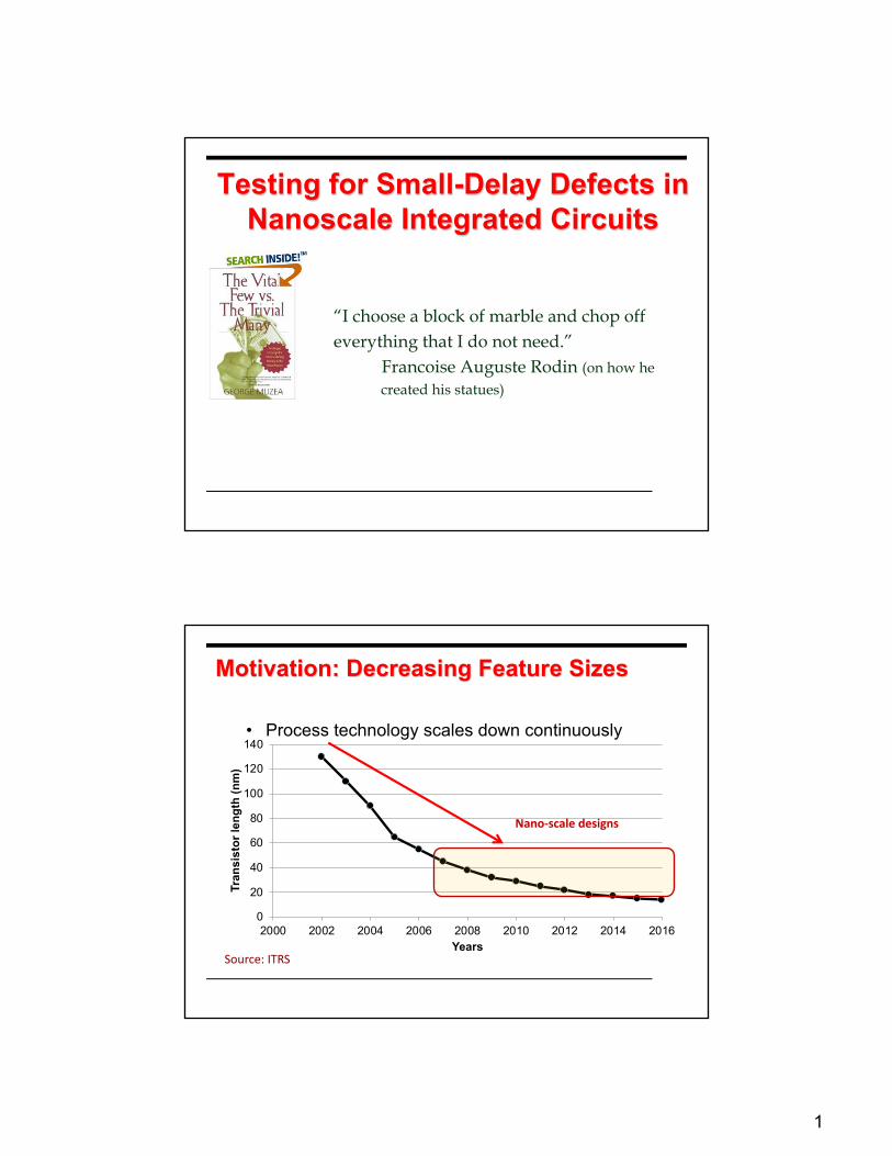
1 Testing for Small - Delay Defects in Nanoscale Integrated Circuits “I choose a block of marble and chop off everything that I do not need.” Francoise Auguste Rodin (on how he created his statues) 0 20 40 60 80 100 120 140 2000 2002 2004 2006 2008 2010 2012 2014 2016 Transistor length (nm) Years Motivation: Decreasing Feature Sizes • Process technology scales down continuously Nano-scale designs Source: ITRS
Transcript of Testing for Small-Delay Defects in Nanoscale Integrated ...
1
Testing for Small-Delay Defects in Nanoscale Integrated Circuits
“I choose a block of marble and chop off everything that I do not need.”
Francoise Auguste Rodin (on how he created his statues)
0
20
40
60
80
100
120
140
2000 2002 2004 2006 2008 2010 2012 2014 2016
Tran
sist
or le
ngth
(nm
)
Years
Motivation: Decreasing Feature Sizes
• Process technology scales down continuously
Nano-scale designs
Source: ITRS

2
Motivation: Increasing Defect Rates• Sub-wavelength lithography (193 nm wavelength)
020406080
100120140
2000 2002 2004 2006 2008 2010 2012 2014 2016
Tran
sist
or le
ngth
(n
m)
Resistive opens Resistive shortsLine edge roughness
and residues
Motivation: Increasing Defect Rates• Random dopant fluctuations in short transistor channel
020406080
100120140
2000 2002 2004 2006 2008 2010 2012 2014 2016
Tran
sist
or le
ngth
(n
m)
Transistor threshold voltage variations
increase
3σ = 30%
3
Motivation: Increasing Defect Rates• Closer wires
0
20
40
60
80
100
120
140
2000 2002 2004 2006 2008 2010 2012 2014 2016
Tran
sist
or le
ngth
(nm
)
Cc
Cc
90nm
45nm
Increased crosstalk effect
Motivation: Increasing Defect Rates• Significant dynamic power density differences across the die
020406080
100120140
2000 2002 2004 2006 2008 2010 2012 2014 2016
Tran
sist
or le
ngth
(n
m)
YPow
er D
issi
patio
n
X
It may cause- Voltage droop
- Power supply variations

4
Motivation: Most Defects Cause SDDs
• All of these defects may cause small-delay defects (SDDs)
• Main contributors of SDDs– Transistor parameter variations– Power supply variations– Crosstalk– Resistive shorts and opens
Background• High test-data volume and test-application times
– Test-data volume 38x higher in 2015 than in 2007 – Test application time 17x higher in 2015 than in 2007
• Many new types of defects cannot be accurately modeled using existing fault models. – Need to model the quality of test patterns such that they can be quickly
assessed for defect screening• Test selection is required to choose the most effective pattern
sequences from large test sets (pattern grading)– Reorder patterns to reduce test time for abort-on-first-fail– Reduce pattern count for production test– Reduce CPU time for generating these patterns
• Common industry practice for test selection is based on fault grading– Computationally expensive– Must be repeated for every fault model

5
A Typical Motivating Scenario(Acknowledgment: Phil Nigh, IBM)
• Semiconductor chip manufacturer needs to test 1 M copies of a chip with 10 K patterns (abort-on-fail)
• Typically only 2000 of the 10 K patterns are “unique fail patterns”– 70%-90% of production test patterns are useless (Ferhani et al.,
Stanford/IBM data, VTS 2008; Guo at al., Intel data, VTS 2006; Madge et al., LSI data, ITC 2004))
– How do we tell which patterns to drop?– The 80/20 rule, The Vital Few versus The Trivial Many– Test economics challenge
• Majority of the fail patterns (e.g., 1800 out of 2000) occur in the first 5 K patterns
• Can we predict which 200 patterns of the next 5000 must be applied?• Currently, all 5 K remaining patterns must be applied to get low
DPM!
Shortcomings of Current Methods for Delay-Defect Test
• Stuck-at fault model alone not sufficient for
high-quality test
• Traditional transition-test ATPG does
not target small-delay defects (SDDs)
– Inclined to select short activation paths
– SDDs are observable on short-slack paths (long
paths)
• Timing-aware ATPG tools have now emerged
– Recent versions of Mentor Graphics FastScan,
Cadence TrueTime ATPG, Synopsys TetraMax
– Problems: High run times for large circuits, not
addressing process variations, not layout-aware,
over-reliance on static timing analysis and path
enumeration
# of parts
Additional delay
Small delay defects
Large delay defects
Sato et al., 2005

6
Short-Path Sensitization
ECE 538 12
Statistical Delay Quality Level (SDQL)
(2) undetected(3) detected
(1) timing-redundant
4 6
63
51
–1
6
3

7
Alternative Approach• Strategy:
– Use “output deviations” as a surrogate coverage-metric for test generation, pattern grading, seed selection for LBIST, and test compression
– Use a flexible, but general, probabilistic fault model to generate a probability map for a logic circuit
– Target multiple fault sites in a probabilistic manner• Compatible with existing test development flows• Useful for addressing phenomenon or mechanisms that are not fully
understood
• Premise: Higher the deviation, better the quality of a test pattern• Automation tools are being implemented for efficiently
computing output deviations and grading test patterns for industrial circuits
IWLS 2005 BenchmarksBenchmark Fault Count Flip-Flop
CountDescription
wb_dma 31,254 881 WISHBONE DMA/Bridge IP Core
tv80 40,022 359 TV80 8-Bit Microprocessor Core
systemcaes 52,544 670 SystemC AES
mem_ctrl 54,440 1,138 WISHBONE Memory Controller
usb_funct 87,658 1,766 USB function core
ac97_ctrl 98,702 2,289 WISHBONE AC 97 Controller
aes_core 106,054 554 AES Cipher
dma 143,620 2,197 Direct Memory Access (DMA) Controller
pci_bridge 168,844 3,677 PCI Interface
wb_conmax 223,252 818 WISHBONE Conmax IP Core
ethernet 745,778 10,545 Ethernet IP core
vga_lcd 1,218,75617,102 WISHBONE rev.B2 compliant Enhanced VGA/LCD
Controller
netcard 6,647,092 97,381 Network Card Controller
leon3mp 6,896,250108,839 32-bit processor compliant with SPARC V8
architecture

8
IWLS 2005 Benchmarks• RTL models are available on IWLS website:
http://www.iwls.org/iwls2005/benchmarks.html• Netlist and layout-generation flow:
RTL
StdCell Libraries
Synopsys Design
Compiler
Scan StitchedFlat Netlist
Synopsys Astro
Layout (DEF)
Challenge: ATPG for Small-Delay Defects
Timing-aware ATPG CPU time relative to TDF ATPG
11x
3x
10x 9x
63x
18x
51x
12x
64x
42x 44x
27x25x
0.00E+00
1.00E+06
2.00E+06
3.00E+06
4.00E+06
5.00E+06
6.00E+06
7.00E+06
0.00
10.00
20.00
30.00
40.00
50.00
60.00
70.00
80.00
90.00
100.00
wb_dm
atv8
0
syste
mcaes
mem_ctrl
usb_
funct
ac97
_ctrl
aes_
core
dma
pci_bri
dge
wb_co
nmax
ethern
et
vga_
lcd
netca
rd
leon3mp
# of
faul
ts
Rel
ativ
e C
PU ti
me
IWLS 2005 Benchmarks
Relative CPU time # faults
Commercial ATPG tool

9
2.8x
1.4x
4.3x
1.8x
3.3x 3.1x
8.2x
2.0x
3.4x
1.1x
1.6x1.2x 1.0x 1.0x
0.00E+00
1.00E+06
2.00E+06
3.00E+06
4.00E+06
5.00E+06
6.00E+06
7.00E+06
0.00
1.00
2.00
3.00
4.00
5.00
6.00
7.00
8.00
9.00
10.00
wb_dm
atv8
0
syste
mca
es
mem
_ctrl
usb_
func
t
ac97
_ctrl
aes_
core
dma
pci_
brid
ge
wb_co
nmax
ethe
rnet
vga_
lcd
netc
ard
leon3
mp
# of
faul
ts
Rel
ativ
e te
st p
atte
rn c
ount
IWLS 2005 Benchmarks
Relative test pattern count # faults
High Pattern Count• Commercial timing-aware ATPG tools lead to large number of patterns
Limitations of Existing Methods (AMD Circuits)• TA ATPG is expensive (compared to TDF
ATPG)
16.73 15.76
12.47
9.0811.45
22.34
10.35
5.76
8.87 9.39
6.39
15.08
4.65
8.22
0.00E+00
2.00E+05
4.00E+05
6.00E+05
8.00E+05
1.00E+06
1.20E+06
1.40E+06
1.60E+06
1.80E+06
0
5
10
15
20
25
Circuit 1 Circuit 2 Circuit 3 Circuit 4 Circuit 5 Circuit 6 Circuit 7
# of
faul
ts
Rel
ativ
e C
PU ti
me
and
Patte
rn C
ount
Industrial circuit blocks
Relative CPU time Relative Pattern Count # faults
10
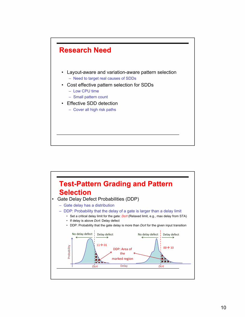
Research Need
• Layout-aware and variation-aware pattern selection– Need to target real causes of SDDs
• Cost effective pattern selection for SDDs– Low CPU time– Small pattern count
• Effective SDD detection– Cover all high risk paths
Test-Pattern Grading and Pattern Selection
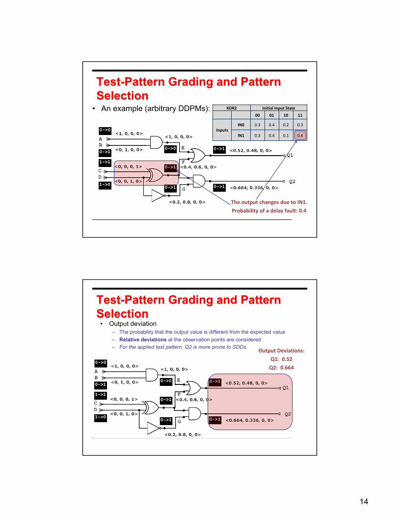
• Gate Delay Defect Probabilities (DDP)– Gate delay has a distribution– DDP: Probability that the delay of a gate is larger than a delay limit
• Set a critical delay limit for the gate: Dcrt (Relaxed limit, e.g., max delay from STA)• If delay is above Dcrt: Delay defect• DDP: Probability that the gate delay is more than Dcrt for the given input transition
Dcrt Dcrt
11à 0100à 10
Delay
Prob
abili
ty
DDP: Area of the
marked region
No delay defect Delay defect No delay defect Delay defect

11
Test-Pattern Grading and Pattern Selection
• Delay Defect Probability Matrix (DDPM)– Includes DDPs for all input à output timing arcs– Example: DDPM for an OR2 gate (entries are arbitrary)
OR2, DDPs Initial Input State [IN0,IN1]
00 01 10 11
InputsIN0 0.2 0 0.4
0.1IN1 0.2 0.2 0
01à0
1à0
Out
put V
olta
ge
Time
VDD
0.80.2
Test-Pattern Grading and Pattern Selection• Signal Transition Probabilities (STPs)
– Delay-fault test-patterns will force signal transitions on circuit nets– 4 different signal transitions are possible:
• Low à Low, Low à High, High à Low, High à High
– Each of these events has a probability to occur– Each net has a vector of signal-transition probabilities:
• Net (Wire): <PLàL , PLàH , PHàL , PHàH>
Out
put V
olta
ge
Time
VDD
Out
put V
olta
ge
Time
VDD
Out
put V
olta
ge
Time
VDD
–utp
utV
olta
ge
Time
VDD

12
Example
< 0.2, 0.8, 0, 0 >
< 0.4, 0.6, 0, 0 >
< 0.616, 0.384, 0, 0 >
AND2 Initial Input State [IN0,IN1]
Prob. 00 01 10 11
Inpu
ts IN00.2
0.3 0 0.2
IN1 0 0.2 0.3
• Both A and B stay @ LOW à No delay defect activated:0.2 * 0.4 = 0.08 (Z stays @ LOW, no defect)
• A or B stays @ LOW and the other input switches à No delay defect activated:0.2 * 0.6 + 0.4 * 0.8 = 0.44 (Z stays @ LOW, no defect)
• Both A and B make LOW à HIGH transition:• Delay-defect: 0.8 * 0.6 * 0.2 = 0.096 (Z stays @ LOW, defect case)• No defect: 0.8 * 0.6 * ( 1 - 0.2 ) = 0.384 (Z goes LOW à HIGH, no defect)
• Overall output STP: Z = < 0.08 + 0.44 + 0.096, 0.384, 0, 0 > = < 0.616, 0.384, 0, 0
AB Z
< PLàL , PLàH , PHàL , PHàH >
Test-Pattern Grading and Pattern Selection
• An example (arbitrary DDPMs):
Initialization of signal transition probabilities on INs
Expected signal transitions are shown in dark boxes

13
Probabilistic Delay-Fault Model and Output Deviations• Propagation of Signal-transition probabilities (STPs)
– The nets connected to the test-application points: Initialization nets (INs) à Initialized with “0” DDP
– During signal propagation through circuit, use DDPM of the gates to update signal-transition probabilities
• Net: <PLàL , PLàH , PHàL , PHàH>
The probability that net A will haveexpected signal-transition, PEXPECTED
Deviation: 1 - PEXPECTED
Test-Pattern Grading and Pattern Selection
• An example (arbitrary DDPMs):
There is no transition on net E.The probability of a delay fault (deviation) is 0.
14
Test-Pattern Grading and Pattern Selection
• An example (arbitrary DDPMs): XOR2 Initial Input State00 01 10 11
InputsIN0 0.3 0.4 0.2 0.3
IN1 0.3 0.4 0.1 0.4
The output changes due to IN1.Probability of a delay fault: 0.4
Test-Pattern Grading and Pattern Selection
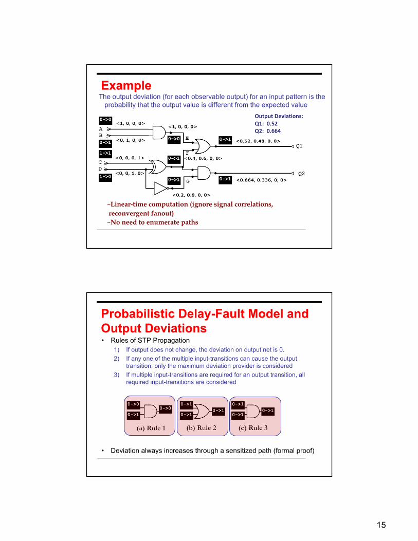
• Output deviation– The probability that the output value is different from the expected value– Relative deviations at the observation points are considered– For the applied test pattern, Q2 is more prone to SDDs Output Deviations:
Q1: 0.52Q2: 0.664
15
ExampleThe output deviation (for each observable output) for an input pattern is the
probability that the output value is different from the expected valueOutput Deviations:Q1: 0.52Q2: 0.664
–Linear-time computation (ignore signal correlations, reconvergent fanout)–No need to enumerate paths
Probabilistic Delay-Fault Model and Output Deviations• Rules of STP Propagation
1) If output does not change, the deviation on output net is 0.2) If any one of the multiple input-transitions can cause the output
transition, only the maximum deviation provider is considered3) If multiple input-transitions are required for an output transition, all
required input-transitions are considered
• Deviation always increases through a sensitized path (formal proof)

16
Test-Pattern Grading and Pattern Selection
• Pattern selection method– For each pattern, calculate output deviations for all
outputs– Drop ineffective patterns on the fly (apply a lower
deviation threshold)– For each output, keep a list of most effective patterns
• Final pattern ordering– The patterns effective for most outputs come first– The goal is to quickly increase topological coverage
Pattern Selection
Q1 Q2 Q3P1 P2 P1
P2 P5 P9
P3 P1 P4
P5 P7 P6
Selected Patterns
Observation points
Patterns are ordered according to the deviationthat they caused at the corresponding observation point
We will select 3 patterns

17
Pattern Selection
Q1 Q2 Q3P1 P2 P1
P2 P5 P9
P3 P1 P4
P5 P7 P6
Selected Patterns
Start with the first observation point.
Select P1.
P1
Pattern Selection
Q1 Q2 Q3P1 P2 P1
P2 P5 P9
P3 P1 P4
P5 P7 P6
Selected Patterns
P1
Continue with Q2.Select P2.
P2

18
Pattern Selection
Q1 Q2 Q3P1 P2 P1
P2 P5 P9
P3 P1 P4
P5 P7 P6
Selected Patterns
P1
Continue with Q3.P1 has already selected.
Select P9.
P2
P9
Simulation Results• Generating DDPMs
– HSpice Monte Carlo (MC) simulations• 200 MC simulations • Transistor gate length, L, 3σ = 10%• Threshold voltage, Vth, 3σ = 30%• Gate-oxide thickness, tox, 3σ = 3%

19
Simulation Results• Correlation Between Output Deviations and Path Lengths
– Kendall’s correlation coefficient
– Perfect positive correlation measure: 1
– Near-perfect correlation between output deviations and path lengths!
0
0.1
0.2
0.3
0.4
0.5
0.6
0.7
0.8
0.9
1
s9234
s13207
s15850
s35932
s38417
s38584
ac97_ctrl
aes_core
des_perf
mem
_ctrl
pci_
bridge32
syste
mcaes
tv80
usb_fu
nct
Ken
dall'
s co
rrel
atio
n co
eff.
Benchmarks
Simulation Results• Benchmarks
– IWLS 2005 benchmarks àSynthesized ASIC blocks
• Simulation setup– Commercial ATPG tool
• n-detect TDF ATPG patterns
• TA ATPG patterns
– Servers• Minimum 16 GB RAM• Quad-core Opterons
– In-house tools• Coded in C++
• Comparison Points– Dynamic-timing simulation
[Lee et al, DFT Symp. 2006]
• Approximate path delays are calculated instead of output deviations
• Always selects top 1/3 of patterns
– Timing-aware ATPG• Commercial ATPG tool used
to generated timing-aware ATPG patterns

20
Simulation Results
• CPU time usage
Simulation Results• Long path coverage ramp-up (systemcaes)

21
Simulation Results• Delay-defect injection experiments
– Fault coverage ramp-up (usb_funct)
Layout-aware Output Deviations
• The method of output deviations has been enhanced to target interconnects
• Interconnects play a major role in circuit delays and delay variations [ITRS 2007]– Crosstalk– Process variations on wire geometries
• Interconnect- and layout-awareness is required for realistic results

22
Layout-Aware Output Deviations• Assign a buffer-like DDPM to all
wires• How detailed do we need to
model?• Lumped delay model: Single
DDPM for all connected wires (for each net)– Not accurate enough– May lead to misleading results
Q
CELL-1
CELL-2
CELL-3
CELL-4
A
B
A
M1M2M3M4Via
n1
n2
Net β
Net DDPM
Initial Input State
0 1Net β 0.2 0.3
Layout-Aware Output Deviations• Other options:• Pin to pin delay model:
– More accurate– What if we need more
resolution?• Via to Via delay model:
Model each metal layer separately– Run time penalty:
Is it worth it?
Q
CELL-1
CELL-2
CELL-3
CELL-4
A
B
A
M1M2M3M4Via
n1
n2
Net β
Pin2Pin DDPM Initial Input State0 1
CELL-1/Q à CELL-2/A 0.08 0.10CELL-1/Q à CELL-3/B 0.01 0.01
CELL-1/Q à CELL-4/A 0.16 0.25

23
Layout-Aware Output Deviations
• STP propagation (pin-to-pin delay model)
<0,1,0,0>
<0.1,0.9,0,0><0,1,0,0>
<1,0,0,0>
<0.1,0.9,0,0>
<1,0,0,0> <1,0,0,0> <0.6,0.4,0,0><1,0,0,0>
<0,0,0,1><0,0,0,1>
<0.3,0.7,0,0>
<0.35,0.65,0,0>
<0.4,0.6,0,0>
<0.4,0.6,0,0> <0.45,0.65,0,0>
<0.7,0.3,0,0>0à00à1
0à00à1 0à0
0à0
0à1
0à1 0à1
0à1 0à1
0à1 0à1
1à1 1à10à1 0à1
Output deviation = 0.7
Output deviation = 0.45
Results• Normalized CPU time (normalized by TA ATPG data)
0.00
0.20
0.40
0.60
0.80
1.00
1.20
1.40
1.60
1.80
2.00
wb_dm
atv
80
syst
emca
es
mem
_ctrl
usb_
func
t
ac97
_ctrl
aes_
core
dma
pci_
brid
ge
wb_co
nmax
Nor
mal
ized
CPU
tim
e
Benchmarks
total(n=3) total(n=5) total(n=8) total(n=10) ti-aware

24
Results• Breakdown of CPU time
0
50000
100000
150000
200000
250000
0
0.2
0.4
0.6
0.8
1
1.2
wb_
dma
tv80
system
caes
mem
_ctrl
usb_
func
t
ac97
_ctrl
aes_
core
dma
pci_br
idge
wb_
conm
ax
# of
faul
ts
Rat
io o
f run
-tim
e
Benchmarks
5-detect dev-5 patt_sel-5 fault#
Results
• Fault coverage ramp-up (tv80)
0
5
10
15
20
25
30
0 500 1000 1500 2000
# de
tect
ed d
elay
faul
ts
# patterns
timing-aware dev.based (n=5)

25
Summary of Simulation Results
• The effect of considering interconnect delays– 15-40% more excited long paths
– Less than 15% CPU time penalty when pin-to-pin wire delay model is used
– Significant advantages at low run-time cost
Results for Industry Circuits• Designs
– Four different AMD circuit blocks– Blocks are selected from different functional units
• ATPG– Commercial ATPG tool– n-detect TDF ATPG and TA ATPG patterns
• Simulation environment– Pool of servers (10000+) with at least 16GB of free RAM– Simulation programs were coded in C++
Design FunctionalityCircuit A Cache relatedCircuit B In execution unitCircuit C In execution unitCircuit D In load-store unit

26
Experimental Results• Normalized number of sensitized long paths
(Long path limit = 70% CLK)
0.00
0.50
1.00
1.50
2.00
2.50
3.00
3.50
Circuit A Circuit B Circuit C Circuit D
Nor
mal
ized
# L
ong
Path
s
Circuits
n=1
n=1 (dev)
n=3
n=3 (dev)
n=5
n=5 (dev)
n=8
n=8 (dev)
ta (σ=25%)
ta (σ=25%) (dev)
ta (σ=0%)
ta (σ=0%) (dev)
Results for AMD Circuits• Normalized number of test patterns (Long path limit = 70% CLK)
9.80
4.56
7.64
1.221.65
0.66
2.30
0.110.00
2.00
4.00
6.00
8.00
10.00
12.00
Circuit A Circuit B Circuit C Circuit D
Nor
mal
ized
Pat
tern
Cou
nt
Circuits
n=1
n=1 (dev)
n=3
n=3 (dev)
n=5
n=5 (dev)
n=8
n=8 (dev)
ta (σ=25%)
ta (σ=25%) (dev)

27
Results for AMD Circuits• Normalized CPU time usage (Long path limit = 80% CLK)
12.66
7.38
17.26
1.601.230.17
1.250.03
0.00
2.00
4.00
6.00
8.00
10.00
12.00
14.00
16.00
18.00
20.00
Circuit A Circuit B Circuit C Circuit D
Nor
mal
ized
CPU
tim
e
Circuits
n=1n=1 (dev)n=3n=3 (dev)n=5n=5 (dev)n=8n=8 (dev)ta (σ=25%)ta (σ=25%) (dev)ta (σ=0%)ta (σ=0%) (dev)
Simulation Results• Long path coverage ramp-up (Long path limit = 80% CLK, Circuit A)
28
Conclusions
• Rethinking of the ATPG problem for small-delay defects
• Output deviations provide an effective metric for pattern grading
• Test-pattern selection for small-delay defects at the gate level– Reduce the need for timing-aware ATPG– Low pattern count and less CPU time