Test Architecture Design and Optimization for Three- Dimensional SoCs Li Jiang, Lin Huang and Qiang...
16
Test Architecture Design and O ptimization for Three-Dimensio nal SoCs Li Jiang, Lin Huang and Qiang Xu CUhk Reliable Computing Laboratry Department of Computer Science & Engineering The Chinese University of Hong Kong
-
Upload
chad-walsh -
Category
Documents
-
view
214 -
download
0
Transcript of Test Architecture Design and Optimization for Three- Dimensional SoCs Li Jiang, Lin Huang and Qiang...
Test Architecture Design and Optimization for Three-Dimensional SoCs
Li Jiang, Lin Huang and Qiang XuCUhk Reliable Computing Laboratry
Department of Computer Science & Engineering
The Chinese University of Hong Kong

Outline
Introduction Motivation Proposed approach Experiments Conclusion

Introduction
3D technique• Vertically stack dices
• TSV as interconnect
Benefit of 3D IC• Interconnect
• Performance, Power, Area
• Memory bandwidth
• Heterogeneous technology• 3D SoCs
Device Layer
TSVCu
Bulk Si
Cu Bond Pad
TSV
DeviceLayer
Metal
Layer 1
Layer 2

Bonding Methods in 3D Technology
W2W bonding• Bond->Cut->Package Test
• Low yield
D2D/D2W bonding• Utilize pre-bond test
• Test->Cut->Bond
• Only stack KGD

TAM1
TAM2
TAM3
3D Chip
5
4 6
1 2 3
5
Layer 1 Layer 2
Idle Idle
Empty
Empty
Post-Bond Test Pre-Bond Test
4 6
1 2 3
After Move
Motivation
Traditional SoC test architecture optimization
3D SoC test architecture optimizationTAM1
TAM2
TAM3
3D Chip
5
4 6
1 2 3
5
Layer 1
3
Layer 2
Idle Idle
Empty
Empty
1 2
4 6
Post-Bond Test Pre-Bond TestMove 1 bit from TAM 3 to TAM 2
TAM1
TAM2
TAM3
5
4 6
1 2 3
Post-Bond Test

Problem Definition
• Given• Set of cores, Test Parameters, Position
• Available TAM width
• Determine• Number of TAM
• Core assignment
• Width of each TAM
• Objective• Minimize the total test cost
• CTotal = CTest-Time * α+ CWire-Length *(1- α)
• CTest-Time = C3DChip + Σ CLayer
• CWire-Length depends on routing model
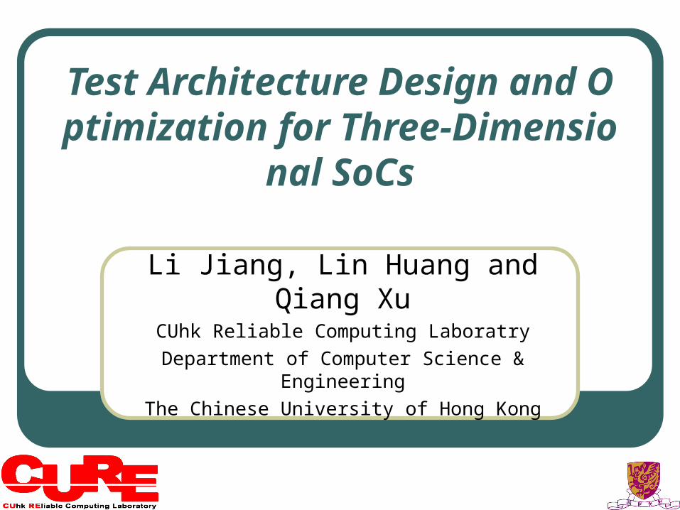
Routing Model
TAM for post-bond test • TAM segments for pre-bond test
• Additional test pad
• TSV linking segments together
Routing cost model• Wire length:
• Manhattan distance between core centers
• Neglect length of TSV
• Wire length * TAM width
1 2
4 2'
3
5TSV
6
TAM1
TAM2
TAM3 TAM2
Wrapper
Layer 1
Layer 2

Approach Simulated annealing
• Appropriate for this scale
• Solution representation• Core assignment & TAM width
• Move• Move core
• Change TAM width
• Large solution space
Proposed approach• Outer SA-based core assignment
• Inner TAM width distribution heuristic
(Core1,Core2) ,(Core5,Core7,Core8)
TamWidth1,TamWidth2
(Core1,Core2,Core5) ,(Core7,Core8)
TamWidth1,TamWidth2
(Core1,Core2) ,(Core5,Core7,Core8)
(Core1,Core2,Core5) ,(Core7,Core8)
TamWidth1,TamWidth2
TamWidth1,TamWidth2
Heuristic
Heuristic

Approach
Overflow
Outer SA-based core assignment• Redundancy in representation
• Rules to eliminate redundancy• 1-to-1 corresponding betweenrepresentation and solution
• Prove of completeness
(C1,C3),(C2,C4,C5)
(C3,C1),(C2,C4,C5)
Initial Solution
Move
Inner TAM Width Distribution Heuristic
Record Cost
Check Temperature
Check Temperature

Approach
Greedy inner TAM width allocation procedure
Set b = 1
Find a TAM Brings the Min Cost
Record Test Cost
Whether can Reduce Test Cost?
b = b+1
No YesTAM Width=0?
YesStop
Assign 1 bit to each TAM

Experiment Setup Baseline algorithms
• TR-1:• Apply existing optimization algorithm to the 3D SoC layer by layer
• Adjust the TAM width among layers iteratively
• Optimize the pre-bond test architecture
• TR-2:• Apply existing optimization algorithm to the whole 3D chip
• Optimize the post-bond test architecture
Benchmark: ITC02 SoC benchmark Map to 3D SoC Previous wrapper optimization algorithm Testbus as TAM

Experimental Results
Testing Time on p22810
00.20.40.60.8
11.21.41.61.8
2
16 24 32 40 48 56 64
Mil
lion
s
TAM Width
Tes
t T
ime
0
10
20
30
40
50
Tho
usan
dsW
ile
Len
gth
Time,TR-1 Time,TR-2Time,SA WL,TR-1WL,TR-2 WL,SA

Experimental Results
a=0.6,t512505
0
10
20
30
40
50
60
70
80
16 24 32 40 48 56 64
Mil
lion
s
TAM Width
Tes
tin
g T
ime
-1500
500
2500
4500
6500
8500
10500
12500
Wir
e L
engt
h
Time,TR-2Time,SAWL,TR-2WL,SA
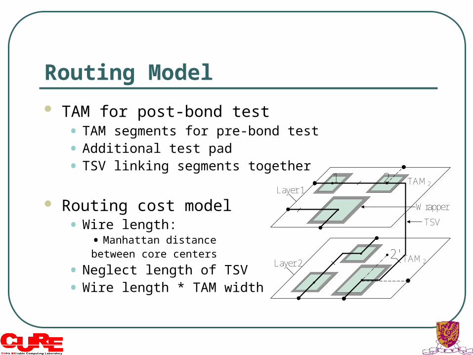
Experimental Results
a=0.4,t512505
0
10
20
30
40
50
60
70
80
16 24 32 40 48 56 64
Mil
lion
s
TAM Width
Tes
ting
Tim
e
-1500
500
2500
4500
6500
8500
10500
12500
Wir
e L
engt
h
Time,TR-2Time,SAWL,TR-2WL,SA
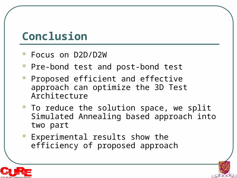
Conclusion
Focus on D2D/D2W Pre-bond test and post-bond test Proposed efficient and effective approach can
optimize the 3D Test Architecture To reduce the solution space, we split Simulated
Annealing based approach into two part Experimental results show the efficiency of proposed
approach

Thank You
Q & A