Temperature and Intensity Dependence of the Limiting ...
12
IEEE JOURNAL OF PHOTOVOLTAICS, VOL. 11, NO. 1, JANUARY 2021 73 Temperature and Intensity Dependence of the Limiting Efficiency of Silicon Solar Cells D. Akira Engelbrecht and Thomas Tiedje Abstract—The temperature and intensity dependence of the lim- iting efficiencies of monofacial and bifacial silicon solar cells are calculated from the physical properties of silicon assuming light trapping by Lambertian scattering from rough surfaces. The maxi- mum efficiency of a bifacial cell (28.92%) is lower than the efficiency of a monofacial cell (29.46%) at room temperature and Air Mass 1.5 Global illumination. The effects of electron–electron interactions on the band gap, radiative recombination rate, and optical ab- sorption are included self-consistently. The temperature coefficient of the output power is -0.23%/°C for the optimum thickness monofacial cell at room temperature. The optimum thickness of silicon solar cells decreases strongly with temperature following a power law T -7 and thin cells have a lower temperature coefficient than thick cells. A surface recombination velocity of 1 cm/s is found to be a turning point below which surface recombination has a small effect on the efficiency. Index Terms—Bifacial solar cells, efficiency limits, intensity dependence, silicon solar cells, surface recombination, temperature dependence. I. INTRODUCTION C RYSTALLINE silicon solar panels are the dominant com- mercial solar cell technology, with annual sales exceed- ing 100 GW globally [1]. For a given insolation level, the efficiency of the solar panel determines the output power and is, therefore, a key factor in the cost of solar electricity. The maximum efficiency of silicon solar cells has been examined theoretically in detail under standard operating conditions con- sisting of Air Mass 1.5 Global illumination (AM1.5 G) and 25 °C operating temperature [2]–[4]. The theoretical calculations typically assume that the silicon solar cells have rough front and/or back surfaces that enhance optical absorption through light trapping. The calculation by Schäfer and Brendel [3] shows that the physical properties of silicon limit the maximum solar cell efficiency to 29.56% under standard operating conditions of AM1.5 G and 25 °C. The theoretical limiting efficiency Manuscript received January 21, 2020; revised March 19, 2020, May 22, 2020, July 22, 2020, and September 9, 2020; accepted October 27, 2020. Date of publication November 26, 2020; date of current version December 21, 2020. This work was supported by the Natural Sciences and Engineering Research Council of Canada. D. Akira Engelbrecht was partially supported by an NSERC Undergraduate Student Research Award. (Corresponding author: Thomas Tiedje.) D. Akira Engelbrecht is with the Mechanical Engineering, University of Vic- toria, Victoria, BC V8W 2Y2, Canada (e-mail: [email protected]). Thomas Tiedje is with the Electrical and Computer Engineering, University of Victoria, Victoria, BC V8W 2Y2, Canada (e-mail: [email protected]). Color versions of one or more of the figures in this article are available online at https://ieeexplore.ieee.org. Digital Object Identifier 10.1109/JPHOTOV.2020.3035115 calculations have been successful in the sense that the limit has been approached quite closely experimentally, but has not been exceeded. The record high measured efficiency for a silicon solar cell is 26.7 ± 0.5% [5], [6] or 90% of the theoretical limit. The theoretical maximum efficiency of silicon solar cells is a useful benchmark in the design of high-efficiency photovoltaic devices and for comparing the performance of silicon solar cells with photovoltaic devices made from other materials [6]. Given the growing importance of solar electricity and the dominant position of silicon, it is useful to extend the calculations of the limiting efficiency to nonstandard operating conditions. Solar panels normally operate above ambient temperature due to heating by sunlight. According to Migan [7], the temperature of a solar panel under full solar illumination is about 20 °C above ambient, although wind reduces the temperature rise [8], [9]. Normal operating temperature is considered to be 45 °C by some manufacturers [10]. In this article, we calculate the limiting cell efficiency and optimum thickness as a function of temperature. Recently there has been growing interest in bifacial solar panels which are sensi- tive to light incident on both sides [11]. Therefore, we calculate the temperature and intensity dependence of the efficiency of bifacial cells as well as conventional single-sided or monofacial cells using a similar method to that used earlier [2]–[4], [12] with the latest values for the relevant material parameters. Several improvements are incorporated into the model itself including a self-consistent treatment of the effect of free carriers on the radiative recombination rate and the optical absorption and more recent data on the Auger recombination rate and free carrier absorption. We also determine the effect of surface recombina- tion on the efficiency for values of the surface recombination velocity in the range that has been observed experimentally. As in the earlier work, we assume that the solar cells consist of silicon sheets that are roughened in order to increase the optical absorption through light scattering. Corrections associated with electron–electron interaction effects are included. Since silicon is available in the form of high purity, low defect density single crystals, we neglect nonradiative recombination at bulk crystal defects and impurities. In this article, intrinsic silicon is consid- ered exclusively because it gives the highest efficiency. II. OPTICAL ABSORPTION Two different optical designs are considered. In the conven- tional, or monofacial, design, the solar cell is a one-sided device consisting of a slab of intrinsic silicon with an antireflection This work is licensed under a Creative Commons Attribution 4.0 License. For more information, see https://creativecommons.org/licenses/by/4.0/
Transcript of Temperature and Intensity Dependence of the Limiting ...

IEEE JOURNAL OF PHOTOVOLTAICS, VOL. 11, NO. 1, JANUARY 2021 73
Temperature and Intensity Dependenceof the Limiting Efficiency of Silicon Solar Cells
D. Akira Engelbrecht and Thomas Tiedje
Abstract—The temperature and intensity dependence of the lim-iting efficiencies of monofacial and bifacial silicon solar cells arecalculated from the physical properties of silicon assuming lighttrapping by Lambertian scattering from rough surfaces. The maxi-mum efficiency of a bifacial cell (28.92%) is lower than the efficiencyof a monofacial cell (29.46%) at room temperature and Air Mass 1.5Global illumination. The effects of electron–electron interactionson the band gap, radiative recombination rate, and optical ab-sorption are included self-consistently. The temperature coefficientof the output power is −0.23%/°C for the optimum thicknessmonofacial cell at room temperature. The optimum thickness ofsilicon solar cells decreases strongly with temperature following apower law T−7 and thin cells have a lower temperature coefficientthan thick cells. A surface recombination velocity of 1 cm/s is foundto be a turning point below which surface recombination has a smalleffect on the efficiency.
Index Terms—Bifacial solar cells, efficiency limits, intensitydependence, silicon solar cells, surface recombination, temperaturedependence.
I. INTRODUCTION
CRYSTALLINE silicon solar panels are the dominant com-mercial solar cell technology, with annual sales exceed-
ing 100 GW globally [1]. For a given insolation level, theefficiency of the solar panel determines the output power andis, therefore, a key factor in the cost of solar electricity. Themaximum efficiency of silicon solar cells has been examinedtheoretically in detail under standard operating conditions con-sisting of Air Mass 1.5 Global illumination (AM1.5 G) and 25°C operating temperature [2]–[4]. The theoretical calculationstypically assume that the silicon solar cells have rough frontand/or back surfaces that enhance optical absorption throughlight trapping. The calculation by Schäfer and Brendel [3] showsthat the physical properties of silicon limit the maximum solarcell efficiency to 29.56% under standard operating conditionsof AM1.5 G and 25 °C. The theoretical limiting efficiency
Manuscript received January 21, 2020; revised March 19, 2020, May 22,2020, July 22, 2020, and September 9, 2020; accepted October 27, 2020.Date of publication November 26, 2020; date of current version December21, 2020. This work was supported by the Natural Sciences and EngineeringResearch Council of Canada. D. Akira Engelbrecht was partially supported byan NSERC Undergraduate Student Research Award. (Corresponding author:Thomas Tiedje.)
D. Akira Engelbrecht is with the Mechanical Engineering, University of Vic-toria, Victoria, BC V8W 2Y2, Canada (e-mail: [email protected]).
Thomas Tiedje is with the Electrical and Computer Engineering, Universityof Victoria, Victoria, BC V8W 2Y2, Canada (e-mail: [email protected]).
Color versions of one or more of the figures in this article are available onlineat https://ieeexplore.ieee.org.
Digital Object Identifier 10.1109/JPHOTOV.2020.3035115
calculations have been successful in the sense that the limithas been approached quite closely experimentally, but has notbeen exceeded. The record high measured efficiency for a siliconsolar cell is 26.7 ± 0.5% [5], [6] or 90% of the theoretical limit.The theoretical maximum efficiency of silicon solar cells is auseful benchmark in the design of high-efficiency photovoltaicdevices and for comparing the performance of silicon solar cellswith photovoltaic devices made from other materials [6]. Giventhe growing importance of solar electricity and the dominantposition of silicon, it is useful to extend the calculations of thelimiting efficiency to nonstandard operating conditions.
Solar panels normally operate above ambient temperature dueto heating by sunlight. According to Migan [7], the temperatureof a solar panel under full solar illumination is about 20 °Cabove ambient, although wind reduces the temperature rise [8],[9]. Normal operating temperature is considered to be 45 °C bysome manufacturers [10].
In this article, we calculate the limiting cell efficiency andoptimum thickness as a function of temperature. Recently therehas been growing interest in bifacial solar panels which are sensi-tive to light incident on both sides [11]. Therefore, we calculatethe temperature and intensity dependence of the efficiency ofbifacial cells as well as conventional single-sided or monofacialcells using a similar method to that used earlier [2]–[4], [12] withthe latest values for the relevant material parameters. Severalimprovements are incorporated into the model itself includinga self-consistent treatment of the effect of free carriers on theradiative recombination rate and the optical absorption and morerecent data on the Auger recombination rate and free carrierabsorption. We also determine the effect of surface recombina-tion on the efficiency for values of the surface recombinationvelocity in the range that has been observed experimentally. Asin the earlier work, we assume that the solar cells consist ofsilicon sheets that are roughened in order to increase the opticalabsorption through light scattering. Corrections associated withelectron–electron interaction effects are included. Since siliconis available in the form of high purity, low defect density singlecrystals, we neglect nonradiative recombination at bulk crystaldefects and impurities. In this article, intrinsic silicon is consid-ered exclusively because it gives the highest efficiency.
II. OPTICAL ABSORPTION
Two different optical designs are considered. In the conven-tional, or monofacial, design, the solar cell is a one-sided deviceconsisting of a slab of intrinsic silicon with an antireflection
This work is licensed under a Creative Commons Attribution 4.0 License. For more information, see https://creativecommons.org/licenses/by/4.0/

74 IEEE JOURNAL OF PHOTOVOLTAICS, VOL. 11, NO. 1, JANUARY 2021
coated front surface and a perfectly reflecting back surface. Thefront and back surfaces of the silicon are both roughened toimprove the optical absorbance by light trapping. The bifacialdevice on the other hand is two-sided with both the front andback surfaces roughened and antireflection coated with no backsurface reflector. This simulates a bifacial solar panel with abifaciality factor of 1 in which the efficiency is the same forillumination on either side. A bifaciality value of 80% hasbeen reported for working solar panels [11]. Field observationswith commercial solar panels show that bifacial solar cells canproduce up to 30% more output power depending on the albedoof the ground and the panel mounting configuration [11].
In the single-sided solar cell, the absorbance can be approxi-mated by [12], [13], [14]
Aj =4αL/j
4αL/j + 1/n2(1)
where j = 1. In the case of the bifacial device, the absorbanceis also given by [1] but with j = 2.L is the thickness of the solarcell, α = αbb + αfc is the optical absorption coefficient, αbb
is the band to band absorption and αfc is the free carrier absorp-tion. The αbb absorption process produces electron-hole pairs,whereas the free carrier absorption αfc produces hot carrierswhich quickly dissipate their excess energy to heat. The indexof refraction is n: the index of refraction can be distinguishedfrom the electron density, for which we use the same symbol, bythe context. Equation (1) is a good approximation in the strongabsorption and weak absorption limits [13].
If the rough front and back surfaces exhibit ideal Lambertianscattering, the optical absorption can be calculated exactly in thegeometrical optics limit [3], [14], in principle improving on theapproximations associated with (1). In this case, the absorbancefor a single-sided cell in which both the front and back surfacesare Lambertian scatterers is [14]
Aj =1 − T 2/j (αL)
1 − (1 − 1
n2
)T 2/j (αL)
(2)
where j = 1. In (2), L is the thickness of the silicon and α isthe optical absorption coefficient. For the bifacial case in whichthere is no back surface mirror and both surfaces are rough andantireflection coated, the absorbance is also given by (2) exceptwith j = 2. The angle-averaged optical transmission T (x) isgiven by
T (x) = e−x (1 − x) + x2E1 (x) . (3)
The last term in (3) includes the exponential integral E1(x),defined by
E1 (x) =
∫ ∞
x
e−u
udu. (4)
Although (2) may be an exact solution in the geometrical opticsapproximation, it is only an approximate solution of the fullelectromagnetic problem [15].
In the low absorption limit, the absorbance in (2) approachesthe value in (1) whereas for αL > 1, the absorbance value in(2) is slightly higher than in (1) and exponentially dependenton thickness [3]. The assumption that rough silicon surfaces
can be approximated as Lambertian scatterers has been testedexperimentally and found to provide a good description ofexperimental data [16]. Modeling the absorbance of silicon withrandom surface textures is discussed in more detail in [14].
Lambertian scattering is a convenient way to describe scatter-ing from rough surfaces that can be realized experimentally, butit is not necessarily the optimum solution to maximize the ab-sorption of solar radiation in a thin layer of silicon. Bhattacharyaet al. [17], [18] have shown through numerical solutions of thefull electromagnetic scattering problem that the absorbance canbe further improved beyond the Lambertian scattering limit withresonant periodic surface patterns.
The free carrier absorption αfc includes contributions fromboth electrons and holes. Experimental measurements show thatfor wavelengths close to the silicon bandgap, the free carrierabsorption as a function of photon energy, temperature, andcarrier density can be parameterized as follows [19], [20]:
αfc =(5.6 × 10⁻⁹λ2.88n+ 6.1 × 10⁻¹²λ2.18p
)T (5)
with units cm−1. In this equation, n and p are the electronand hole densities, assumed to be equal, the wavelength λ ismeasured in centimeters and the temperature in Kelvin.
III. ELECTRON-HOLE RECOMBINATION
We assume that the silicon is undoped and that under illumi-nation, the electron and hole densities, n, p, are equal, and muchlarger than the intrinsic carrier concentration ni or n, p � ni.This will be the case, for example, if the silicon is weaklydoped or intrinsic. We also assume that the ambipolar diffusionlength of the photogenerated electrons and holes is large com-pared to the cell thickness so that the carrier concentration andquasi-Fermi levels are approximately constant throughout thecell. In other words, we neglect carrier concentration gradientsassociated with carrier diffusion to the contacts. Some carrierconcentration gradient is needed to extract carriers, so thisassumption can be regarded as an area for improvement in futuremodeling.
The electron density n and cell output voltage V are relatedby the following equation:
n = ni,eff (T, n) eqV2kT (6)
where the carrier concentration dependence of the intrinsiccarrier concentration ni,eff is due to bandgap narrowing. Theintrinsic carrier concentration ni = ni,eff (T, 0). The tempera-ture and carrier concentration dependence of ni,eff is given by[21], [22]
ni,eff (T, n) = 1.589 × 10¹⁵ T 1.706 e−Eg(T,n)
2kT (7)
where the bandgap Eg(T, n), as a function of temperature andcarrier concentration [23], has been determined by Wolf et al.[24] and Schenk [25] to be
Eg (T, n) = 1.206 − 2.73 × 10⁻⁴T +BGN (T, n) . (8)
BGN(T, n) is the bandgap narrowing caused by electron–electron correlation effects. A mathematical expression forBGN(T, n) is available in [25], which is a small effect under

ENGELBRECHT AND TIEDJE: TEMPERATURE AND INTENSITY DEPENDENCE OF THE LIMITING EFFICIENCY OF SILICON SOLAR CELLS 75
usual operating conditions. We evaluateni at 298.15 K using (7),(8) for low carrier concentrations where the band gap narrowingeffect can be neglected and find ni = 8.28 × 109 cm−3 [24].The estimated one standard deviation measurement accuracy ofthis value is 3% [21], [22].
Non-radiative recombination of electrons and holes at thesurface is an important loss process in solar cells and improve-ment in surface passivation is a subject of active research. In themost efficient silicon solar cells, the front and back surfaces arepassivated with dielectric coatings such as SiO2, AlOx, or SiNx
in order to minimize surface recombination. Surface recombi-nation velocities as low as 0.3 and 0.1 cm/s have been reportedfor silicon passivated with AlOx [4], [26]–[30] and amorphoushydrogenated silicon (a-Si/SiOx/SiNx) heterostructures, respec-tively [31]. The surface recombination velocity is likely to betemperature dependent. In the efficiency calculations in thisarticle, we assume that the electrical contacts are in the formof small area contacts or surface passivating heterojunctionssuch as in the HIT type a-Si/crystalline silicon heterojunctioncells [5], [32]. In the ideal case of small area contacts or surfacepassivating heterojunctions, the effect of the electrical contactson the surface recombination can be neglected.
Auger recombination and radiative recombination are the twomost important intrinsic bulk recombination mechanisms in highpurity silicon. The Auger recombination rate has been measuredas a function of both carrier density and temperature [4], [27],[33]. Under illumination as discussed above, we assume thatthe silicon is under high injection conditions in which casen = p, and n = n0 +Δn � no, p0, where n0 and p0 arethe equilibrium carrier concentrations in the dark; Δn is theexcess carrier concentration caused by the incident light. Thisassumption is valid for high illumination and low doping. In thislimit, the measured room temperature ambipolar Auger lifetimehas been parameterized in three publications [4], [27], [33]. Weuse the results in [4]
1τA
= 2.38 × 10⁻²⁹ n1.93. (9)
The exponent in (9) is slightly less than the classical Augerexponent of two, due to electron–electron correlation effects[27]. For n = 7 × 1015 cm−3, typical of carrier densitiesin solar cells at the maximum power point, the mean Augerlifetime in [4], [27], [33] is 12.0 ± 0.8 ms. The scatter in thedifferent experimental measurements provides an estimate of theexperimental uncertainty in the measured Auger recombinationrate. Taking the ambipolar diffusion coefficient of electrons andholes to be 15 cm2/s [34] and recombination lifetime to be 12 ms,we obtain a carrier diffusion length of 4 mm, well in excess of thesolar cell thicknesses considered in this article. This supports ourassumption that the quasi-Fermi levels are flat inside the solarcell.
We adopt the concentration dependence of the Auger ratefrom Veith-Wolf et al. [4] in (9) and take the temperaturedependence from [33]. In this case, the combined temperatureand concentration dependence of the Auger recombination rate
is
1τA
= CAn1.93 (10)
where
CA =
[1.58 × 10⁻²⁷
(T − 193)+ 3.01 × 10⁻³² T
]. (11)
The temperature dependence of the Auger coefficient in (11)was obtained from measurements over the temperature range243–473 K, at a carrier concentration n = 5 × 1016cm−3 [33].We assume that the temperature dependence of the Auger coeffi-cient in (11) is still valid for carrier densities in the wider range of5 × 1015 < n < 3 × 1016 cm−3 typical of carrier concentrationsin operating solar cells at the maximum power point, since wehave no experimental data on the temperature dependence of theAuger coefficient at different carrier concentrations. The highestcarrier densities will be present in the thinnest solar cells at thehighest operating temperatures.
The radiative recombination coefficient B can be computedfrom αbb, the interband optical absorption coefficient as afunction of photon energy following the principle of detailedbalance. Detailed balance requires that the generation rate ofelectron hole pairs by thermal blackbody radiation be equal tothe radiative recombination rate. In this case [12],
B n2i = 8π
∫αbb
n2c
λ4e−
hcλkT dλ (12)
where the left-hand side is the radiative recombination rateand the right-hand side is the generation rate due to ambienttemperature black body radiation. The “ni” in (12) is the intrinsicelectron density and the “n” in the integral is the index of refrac-tion, which depends weakly on temperature and photon energy.Measurements of the interband optical absorption coefficientαbb
have been published by Green [35] for temperatures in the range−24 to +200 °C and also by Nguyen et al. [36]. Green providesan interpolation formula with tabulated coefficients so that theoptical absorption can be determined for arbitrary temperaturesin the −24 to 200 °C range (249–473 K) as follows:
αbb (λ, T ) = αbb (λ, 300)
(T
300
)b(λ,T )
(13)
where T is in Kelvin.The radiative recombination rate is found experimentally to
be dependent on the electron density [37]. The reason for thedependence on carrier density is that electrons and holes tend toattract each other, which enhances the radiative recombinationrate. However, at high carrier densities, the Coulomb attraction isreduced by screening which tends to reduce the radiative recom-bination rate. At high temperatures, the thermal motion of theelectrons and holes tends to diminish this screening effect. Theeffect of the photogenerated electrons and holes on the radiativerecombination rate is described by the dimensionless parame-ter BRel(n, T ) where 0 < BRel < 1 [37], [38]. The radiativerecombination rate in photo-excited silicon is B∗ = BRel B.Experimental data on BRel as a function of carrier density andtemperature are available for the temperature range from 101
76 IEEE JOURNAL OF PHOTOVOLTAICS, VOL. 11, NO. 1, JANUARY 2021
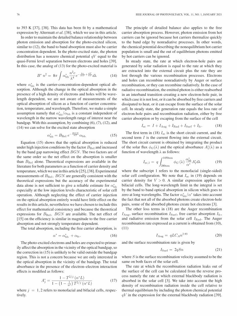
to 393 K [37], [38]. This data has been fit by a mathematicalexpression by Altermatt et al. [38], which we use in this article.
In order to maintain the detailed balance relationship betweenphoton emission and absorption for the photo-excited silicon,similar to (12), the band to band absorption must also be carrierconcentration dependent. In the photo-excited state, the photondistribution has a nonzero chemical potential qV equal to thequasi-Fermi level separation between electrons and holes [39].In this case, the analog of (13) for the photo-excited material is
B∗ n2 = 8π∫
α∗bb
n2c
λ4e−
hcλkT + qV
kT dλ (14)
where α∗bb is the carrier-concentration-dependent optical ab-
sorption. Although the change in the optical absorption in thepresence of a high density of electrons and holes will be wave-length dependent, we are not aware of measurements of theoptical absorption of silicon as a function of carrier concentra-tion, temperature, and wavelength. Therefore, we make a simpleassumption namely that α∗
bb/αbb is a constant independent ofwavelength in the narrow wavelength range of interest near thebandgap. With this assumption, by combining (6), (7), (12), and(14) we can solve for the excited state absorption
α∗bb = BRel e
−BGNkT αbb. (15)
Equation (15) shows that the optical absorption is reducedunder high injection conditions by the factor BRel and increasedby the band gap narrowing effect BGN . The two factors are ofthe same order so the net effect on the absorption is smallerthan BRel alone. Theoretical expressions are available in theliterature for both parameters as a function of carrier density andtemperature, which we use in this article [25], [38]. Experimentalmeasurements of BRel, BGN are generally consistent with thetheoretical expressions but the accuracy of the experimentaldata alone is not sufficient to give a reliable estimate for α∗
bb
especially at the low injection levels characteristic of solar celloperation. Although neglecting the effect of carrier injectionon the optical absorption entirely would have little effect on theresults in this article, nevertheless we have chosen to include thiseffect for mathematical consistency and because the theoreticalexpressions for BRel, BGN are available. The net effect of[15] on the efficiency is similar in magnitude to the free carrierabsorption and not strongly temperature dependent.
The total absorption, including the free carrier absorption, is
α∗ = α∗bb + αfc. (16)
The photo-excited electrons and holes are expected to primar-ily affect the absorption in the vicinity of the optical bandgap, sothe correction in (15) is unlikely to be valid outside the bandgapregion. This is not a concern because we are only interested inthe optical absorption in the vicinity of the bandgap. The totalabsorbance in the presence of the electron–electron interactioneffects is modified as follows:
A∗j =
1 − T 2/j (α∗L)1 − (
1 − 1n2
)T 2/j (α∗L)
(17)
where j = 1, 2 refers to monofacial and bifacial cells, respec-tively.
The principle of detailed balance also applies to the freecarrier absorption process. However, photon emission from hotcarriers can be ignored because hot carriers thermalize quicklyto the band edge by nonradiative processes. In other words,the chemical potential describing the nonequilibrium hot carrierpopulation is small and the out of equilibrium photons emittedby hot carriers can be ignored.
In steady state, the rate at which electron-hole pairs aregenerated by solar radiation is equal to the rate at which theyare extracted into the external circuit plus the rate they arelost through the various recombination processes. Electronsand holes can recombine nonradiatively by Auger or surfacerecombination, or they can recombine radiatively. In the case ofradiative recombination, the emitted photon is either reabsorbedin an interband transition creating a new electron-hole pair, inwhich case it is not lost, or it can be absorbed by free carriers anddissipated to heat, or it can escape from the surface of the solarcell. In steady state, the generation rate equals the loss rate ofelectron-hole pairs and recombination radiation, either by freecarrier absorption or by escaping from the surface of the cell
Isc = I + IAug + IRad + ISurf + Ifc. (18)
The first term in (18) Isc is the short circuit current, and thesecond term I is the current flowing into the external circuit.The short circuit current is obtained by integrating the productof the solar flux φG(λ) and the optical absorbance A∗
1(λ) as afunction of wavelength λ as follows:
Isc,1 = q
∫ 1450nm
280nmφG (λ)
α∗bb
α∗ A∗1dλ (19)
where the subscript 1 refers to the monofacial (single-sided)solar cell configuration. We note that Isc in (19) depends oncarrier density for V > 0. A similar expression applies forbifacial cells. The long-wavelength limit in the integral is setby the band to band optical absorption in silicon which goes tozero at long wavelengths. The factor α∗
bb/α∗ takes into account
the fact that not all of the absorbed photons create electron-holepairs, some of the absorbed photons create hot electrons [3].
The other loss terms in (18) are the Auger recombinationIAug, surface recombination ISurf , free carrier absorption Ifc,and radiative emission from the solar cell IRad. The Augerrecombination rate expressed as a current is obtained from (10),(11)
IAug = qLCAn2.93 (20)
and the surface recombination rate is given by
ISurf = 2qSn (21)
where S is the surface recombination velocity assumed to be thesame on both faces of the solar cell.
The rate at which the recombination radiation leaks out ofthe surface of the cell can be calculated from the reverse pro-cess namely the rate at which external blackbody radiation isabsorbed in the solar cell [3]. We take into account the highdensity of recombination radiation inside the cell relative tothermal equilibrium by including the photon chemical potentialqV in the expression for the external blackbody radiation [39].

ENGELBRECHT AND TIEDJE: TEMPERATURE AND INTENSITY DEPENDENCE OF THE LIMITING EFFICIENCY OF SILICON SOLAR CELLS 77
To simplify the integrals, we introduce the following expressionfor the blackbody photon flux per unit solid angle in free space:
b (λ, V ) =2cλ4
e−hc
λkT + qVkT . (22)
With this notation, the recombination radiation flux that isemitted from the surface of the solar cell, expressed as a current,for monofacial and bifacial solar cells is
IRad, j = jπq
∫α∗bb
α∗ A∗jbdλ. (23)
Recombination radiation can escape from both the front andback surfaces of the bifacial cell (j = 2), which accounts for theextra factor of two in this case. Strictly speaking, the blackbodyradiation flux in (23) should be the net flux b(λ, V )− b(λ, 0);however, the equilibrium flux in the dark b(λ, 0) is much smallerthan b(λ, V ) at open circuit or the maximum power point and isneglected.
The rate at which recombination radiation is generated per unitvolume is given by (14). Some of this radiation escapes out thesurface(s) of the solar cell and is lost, as described by (23). Theremainder of the radiation is absorbed either through interbandtransitions that create new electron-hole pairs or through freecarrier absorption. The absorbed radiation can be computed bysubtracting the radiation escaping from the cell in (23) from thetotal radiation emitted in the radiative recombination process in(14) for the monofacial and bifacial cells
IAbs,j = jπq
∫α∗bb
α∗(4α∗n2L/j −A∗
j
)b dλ. (24)
The absorption in (24) is a combination of band to band tran-sitions and free carrier absorption. The band-to-band part ofthe absorption is not a loss process because it produces newelectron-hole pairs and has been referred to as photon recycling[40]. The free carrier part of the absorption, which is a lossprocess, is a fraction of the absorption given by
Ifc,j = jπcq
∫αfc
α∗α∗bb
α∗(4α∗n2L/j −A∗
j
)b dλ. (25)
The factor α∗fc/α
∗ is the fraction of the total absorbed photonsthat are absorbed by free carriers as discussed above. The photoncurrent that is recycled into the band to band absorption can beobtained by replacing αfc/α
∗ in (25) with α∗bb/α
∗
IRecyc,j = jπq
∫ (α∗bb
α∗
)2 (4α∗n2L/j −A∗
j
)b dλ. (26)
For a better physical understanding of (24)–(26), it is helpful tosubstitute the approximate expressions for the absorbance from(1).
IV. SOLAR CELL PERFORMANCE
Equation (18) is solved numerically for the current I , voltageV , and maximum output power using MATLAB. The maximumpower point is found by iteratively solving P = IV where Iand V are expressed as a function of n until the maximum powercondition dP (n)/dn = 0 is reached. The current and voltage atthe maximum power point are Imp, Vmp, respectively. A similar
approach is taken to solve for the open-circuit voltage, Voc. Voc
is found by iteratively solving P = IV for the open-circuitcondition where P (n) = 0 and n �= ni. All integrations wereperformed using MATLAB’s implementation of trapezoidal in-tegration. The short circuit current Isc, was calculated using theAM1.5 G 37° tilt, reference solar spectrum generated accordingto the ASTM specifications [41]. The spectrum was multipliedby 0.9971 so that the integrated solar flux is 100 mW/cm2 inthe wavelength range from 280 to 4000 nm. The absorptioncoefficients and index of refraction of silicon were interpolatedto the wavelength values of the AM1.5 G solar spectrum usingMATLAB’s implementation of piecewise cubic interpolation.The fill factor is defined as FF = ImpVmp/IscVoc and theefficiency is η = ImpVmp/100 mW.
For the intensity dependence, we used the Air Mass 1.5 Directsolar spectrum [41], multiplied by a dimensionless constant Cbetween 10-3 and 103. The total incident intensity was calculatedfrom
Ptotal = C
∫ 4000nm
280nm
hc
λφD (λ) dλ. (27)
In this case, φD(λ) is the part of the solar spectrum in thedirect beam of the sun. The upper and lower bounds on theintegral are artificial but there is only a very small fraction ofthe solar spectrum outside this wavelength range.
Values for the efficiency of monofacial silicon so-lar cells at room temperature (25 °C = 298.15 K)and AM1.5 G taken from the literature are shown inTable I. The first row in Table I is Richter et al.’s [2] resultsfor the limiting efficiency using up-to-date (2013) values for thematerial parameters and including the electron-electron interac-tion effects that reduce the bandgap and radiative recombinationrate and modify the Auger recombination rate. The second rowcontains the device parameters for the record-setting siliconsolar cell of Yoshikawa et al. [5], with the highest measured ef-ficiency to date under standard conditions. Schäfer and Brendel[3] calculated the limiting efficiency using a similar method toRichter et al. [2] except that the improved approximation for theoptical absorbance in (2) was used. Our results for monofacialcells, which are shown in Table II, are similar to Schäfer andBrendel’s results as expected. We find an optimum thickness of99.9 μm, close to the 98.1 μm found in [3]. The small reductionin efficiency relative to [3] is due to the slightly larger Augerrecombination rate in [4] compared with [27]. Other changes,namely the use of a more recent higher value for the free carrierabsorption [20], and the carrier density-dependent band-to-bandabsorption have a small effect on the efficiency and contributefractionally to the fourth significant figure in the efficiency.
The final row in Table I is the theoretical calculation byBhattacharya and John [17] for a silicon solar cell with a periodicsurface texture tuned to resonantly enhance the optical absorp-tion in the vicinity of the band edge. The resonant enhancementallows the optical absorption to exceed the absorption enhance-ment produced by scattering from random surface textures. Theenhanced absorption in the band edge region means that thesolar cell can be thinner, which increases the electron-hole pairconcentration and hence the output voltage.

78 IEEE JOURNAL OF PHOTOVOLTAICS, VOL. 11, NO. 1, JANUARY 2021
TABLE ICALCULATED AND MEASURED SILICON SOLAR CELL PERFORMANCE PARAMETERS FROM THE LITERATURE
TABLE IICALCULATED MONOFACIAL AND BIFACIAL SILICON SOLAR CELL PERFORMANCE PARAMETERS
Solar cell performance was calculated for the temperaturerange from 240 to 400 K. The lower limit is an extrapolation ofmeasurements of the optical absorption as a function of temper-ature which extends down to 249 K [35] and the experimentaldata on the temperature dependence of the Auger recombinationwhich has a lower limit of 243 K [33]. On the high-temperatureside, the experimental data on which BRel is based stops at 393K [37] and the free carrier absorption measurements go up to372 K [19]. The last two parameters are relatively small effectsso it is reasonable to extrapolate them to higher temperaturessince the more critical parameters namely optical absorption andAuger recombination data are available up to 473 K [33],[35].The temperature range 240–400 K covers most of the range overwhich commercial silicon solar panels are normally specified foroperation, namely from −40 to +85 °C (233–358 K) [10].
The first row in Table II shows the optimum thickness andelectrical output parameters for a monofacial silicon solar cellunder standard conditions. The remaining four rows in Table IIshow the effects of surface recombination with S = 0.1cm/s, of varying the operating temperature from 240 to 400 K,and of increasing the AM1.5 Direct radiation by a factor of1000, with all other operating parameters kept at the referencevalues. Analogous results for bifacial cells are also shown inTable II.
A number of observations can be made. The optimum thick-ness of the bifacial cell is almost exactly twice the thicknessof the optimum monofacial cell, as explained in the Appendix.According to (1), in the long-wavelength limit, a bifacial cellwill have the same optical absorbance as a monofacial cellwith half the thickness. As a result, the short circuit currentsfor the monofacial and bifacial cells in Table II are almost
identical. The larger thickness of the bifacial cell reduces theoutput voltage and reduces the efficiency by 0.54% absoluteor 1.8% relative. A surface recombination velocity of 0.1 cm/son both front and back surfaces has only a small effect on theefficiency (−0.5% relative). The optimum thickness decreasesstrongly with operating temperature and increases when surfacerecombination is present.
In line with convention in the literature [2], [3], the limitingefficiency in Table II is presented with four significant digits.Since Auger recombination is the most important loss process, itis reasonable to expect the measurement uncertainty in the valueof Auger recombination rate to have an important effect on theaccuracy of the calculated efficiency. As discussed above, undertypical conditions, the experimental Auger lifetime is 12.0± 0.8ms. This uncertainty in the Auger coefficient leads to uncertaintyin the efficiency of 29.46 ± 0.045%.
The intrinsic carrier concentration at room temperature ni
determines the relationship between the output voltage and thecarrier density. The experimental uncertainty in this quantity is±3% [21], [22] which produces uncertainty in the efficiencyof 29.46 ± 0.060%. Combining the two uncertainties leads tothe result that the limiting efficiency of the monofacial solarcell is 29.46 ± 0.08% including the experimental error in theintrinsic carrier concentration and Auger recombination rate.Failures of the optical absorption model to correctly describethe light scattering associated with a random surface texture andexperimental uncertainties in the electron–electron interactioneffects are difficult to quantify and not included.
Table III shows how the various loss processes change forthe different operating conditions included in Table II. We notethat the carrier density at the maximum power point does not

ENGELBRECHT AND TIEDJE: TEMPERATURE AND INTENSITY DEPENDENCE OF THE LIMITING EFFICIENCY OF SILICON SOLAR CELLS 79
TABLE IIICARRIER DENSITIES AND LOSSES AT MAXIMUM POWER POINT IN MONOFACIAL AND BIFACIAL SILICON SOLAR CELLS
Thicknesses are in Table II.
Fig. 1. Efficiency as a function of thickness at 240, 298, and 400 K forAM1.5 G illumination, neglecting surface recombination. The solid lines arefor monofacial cells and the broken lines for bifacial cells.
change very much with temperature. Even a small increase incarrier concentration with temperature would be expected tosignificantly increase the Auger losses, due to the exponent 2.93in the Auger recombination rate. However, the decrease in thick-ness with increasing temperature compensates for the increasein recombination per unit volume, so that the total Auger lossesdon’t change very much with temperature. Nevertheless, Augerrecombination is the dominant loss process under all operatingconditions in Table III. Extrapolating the surface recombinationto S = 1 cm/s suggests that surface recombination will exceedAuger as the dominant loss process when S > 1 cm/s. Even forsmall surface recombination velocities, surface recombinationexceeds radiative losses. Free carrier absorption is small in allcases, even at high temperatures and high solar concentration.
Fig. 2. Optimum thickness as a function of temperature for mono and bifacialcells, as indicated in the legend, for AM1.5 G illumination with surface recom-bination velocities S = 0 and 0.1 cm/s. Both axes are log scales. The two lowerbroken lines show the thickness values where the efficiency drops to 99% ofthe peak efficiency at the optimum thickness. These lines show how much thethickness can be reduced without significant loss in efficiency.
TABLE IVFITTING PARAMETERS FOR OPTIMUM THICKNESS
AS A FUNCTION OF TEMPERATURE
R2 = 0.9997.
V. TEMPERATURE DEPENDENCE
In this section, we show how the limiting efficiency of siliconsolar cells depends on temperature, thickness, and surface

80 IEEE JOURNAL OF PHOTOVOLTAICS, VOL. 11, NO. 1, JANUARY 2021
Fig. 3. Efficiency for mono and bifacial cells as a function of temperature forthe optimum thickness at each temperature and for a fixed thickness equal to theoptimum at 298 K. The illumination is AM1.5 G and surface recombination isneglected.
TABLE VFITTING PARAMETERS FOR LIMITING EFFICIENCY
AS A FUNCTION OF TEMPERATURE
R2 = 0.99996.
Fig. 4. Efficiency of 50, 100, and 200 µm thick monofacial solar cell as afunction of surface recombination velocity at 25 °C and AM1.5 G.
Fig. 5. Losses as a function of temperature expressed as current, for a mono-facial cell at the optimum thickness at each temperature for AM1.5 G and asurface recombination velocity S = 0.1 cm/s. Auger recombination is the mostimportant loss mechanism at all temperatures.
recombination. Fig. 1 shows the efficiency as a function ofthickness for monofacial and bifacial solar cells at three differenttemperatures. There is an optimum thickness because if thesilicon is too thin, the cell does not absorb the light and if it istoo thick, the carrier concentration drops and the output voltagegoes down. The efficiency is rather insensitive to thicknessnear the optimum. The reason why the optimum thicknessdecreases with temperature can be explained as follows. Theshort circuit current is a strong function of thickness at smallvalues of L but saturates at large values of L and is onlyweakly dependent on temperature. The open-circuit voltage,on the other hand, depends rather strongly on thickness andtemperature as shown in Table II and there is no saturation.According to (6), V 2kT ln(n) so that dV/dL(2kT/n)dn/dL.If the fractional change in photogenerated carrier density withthickness, (1/n)dn/dL, is weakly dependent on temperature,then the thickness dependence of the output voltage increaseslinearly with temperature. This means that the maximum powerpoint will shift to progressively smaller thicknesses at hightemperature, due to the stronger L dependence of the voltage athigh temperature and the weak L dependence of the current.
Fig. 2 is a log-log plot of the optimum silicon thicknessas a function of temperature for monofacial and bifacial solarcells. The optimum thickness decreases by almost an order ofmagnitude from 184 μm at 0 °C to 19 μm at 100 °C. To a goodapproximation, it follows a power law of the form L = aT−b.The a, b parameter values are given in Table IV: MF, BF meanmonofacial, and bifacial, respectively.
When surface recombination is present, the optimum thick-ness increases because the surface recombination is a smallerfraction of the total recombination when the volume of the
ENGELBRECHT AND TIEDJE: TEMPERATURE AND INTENSITY DEPENDENCE OF THE LIMITING EFFICIENCY OF SILICON SOLAR CELLS 81
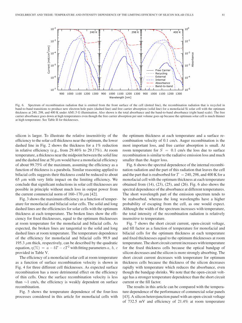
Fig. 6. Spectrum of recombination radiation that is emitted from the front surface of the cell (dotted line), the recombination radiation that is recycled inband-to-band transitions to produce new electron hole pairs (dashed line) and free carrier absorption (solid line) for a monofacial Si solar cell with the optimumthickness at 240, 298, and 400 K under AM1.5 G illumination. Also shown is the total absorbance and the band-to-band absorbance (right hand scale). The freecarrier absorbance goes down at high temperatures even though the free carrier absorption per unit volume goes up because the optimum solar cell is much thinnerat high temperature. See Table II for thicknesses.
silicon is larger. To illustrate the relative insensitivity of theefficiency to the solar cell thickness near the optimum, the lowerdashed line in Fig. 2 shows the thickness for a 1% reductionin relative efficiency (e.g., from 29.46% to 29.17%). At roomtemperature, a thickness near the midpoint between the solid lineand the dashed line at 50μm would have a monofacial efficiencyof about 99.75% of the maximum, assuming the efficiency as afunction of thickness is a parabola. Similar reasoning applied tobifacial cells suggests their thickness could be reduced to about65 μm with very little impact on the limiting efficiency. Weconclude that significant reductions in solar cell thicknesses arepossible in principle without much loss in output power fromthe current commercial norm of 160–170 μm [42].
Fig. 3 shows the maximum efficiency as a function of temper-ature for monofacial and bifacial solar cells. The solid and longdashed lines are the efficiencies for solar cells with the optimumthickness at each temperature. The broken lines show the effi-ciency for fixed thicknesses, equal to the optimum thicknessesat room temperature for the monofacial and bifacial cells. Asexpected, the broken lines are tangential to the solid and longdashed lines at room temperature. The temperature dependenceof the efficiency for monofacial and bifacial cells 99.9 and195.3 μm thick, respectively, can be described by the quadraticequation, η(%) = a− bT − cT 2 with fitting parameters a, b, cprovided in Table V.
The efficiency of a monofacial solar cell at room temperatureas a function of surface recombination velocity is shown inFig. 4 for three different cell thicknesses. As expected surfacerecombination has a more detrimental effect on the efficiencyof thin cells. Once the surface recombination velocity is lessthan ∼1 cm/s, the efficiency is weakly dependent on surfacerecombination.
Fig. 5 shows the temperature dependence of the four-lossprocesses considered in this article for monofacial cells with
the optimum thickness at each temperature and a surface re-combination velocity of 0.1 cm/s. Auger recombination is themost important loss, and free carrier absorption is small. Atroom temperature for S = 0.1 cm/s the loss due to surfacerecombination is similar to the radiative emission loss and muchsmaller than the Auger loss.
Fig. 6 shows the spectral dependence of the internal recombi-nation radiation and the part of this radiation that leaves the celland the part that is reabsorbed for T = 240, 298, and 400 K for amonofacial cell with the optimum thickness at each temperatureobtained from (14), (23), (25), and (26). Fig. 6 also shows thespectral dependence of the absorbance at different temperatures.The short wavelength part of the emission spectrum tends tobe reabsorbed, whereas the long wavelengths have a higherprobability of escaping from the cell, as one would expect.Although the width of the spectrum increases with temperature,the total intensity of the recombination radiation is relativelyinsensitive to temperature.
Fig. 7 shows the short circuit current, open-circuit voltage,and fill factor as a function of temperature for monofacial andbifacial cells for the optimum thickness at each temperatureand fixed thicknesses equal to the optimum thicknesses at roomtemperature. The short circuit current increases with temperaturefor the fixed thickness cells because the optical bandgap ofsilicon decreases and the silicon is more strongly absorbing. Theshort circuit current decreases with temperature for optimumthickness cells because the thickness of the silicon decreasesrapidly with temperature which reduces the absorbance, eventhough the bandgap shrinks. We note that the open-circuit volt-age has a stronger temperature dependence than the short circuitcurrent or the fill factor.
The results in this article can be compared with the tempera-ture dependence of the performance of commercial solar panels[43]. A silicon heterojunction panel with an open-circuit voltageof 732.5 mV and efficiency of 21.4% at room temperature

82 IEEE JOURNAL OF PHOTOVOLTAICS, VOL. 11, NO. 1, JANUARY 2021
Fig. 7. Fill factor, short circuit current, and open circuit voltage as a functionof temperature for mono and bifacial cells under AM1.5 G illumination for theoptimum thickness at each temperature as well as for a fixed thickness equal tothe optimum room temperature thickness with S = 0.
was observed to have a temperature coefficient dVoc/dT =−1.6 meV/K [43]. According to the theory presented here,a solar cell with this output voltage and S = 0 will have atemperature coefficient of−1.8meV/K. A detailed comparisonis presented in a separate publication [44].
Fig. 8. Intensity dependence of the efficiency for mono and bifacial solarcells at room temperature, for S = 0. Only the direct component of the AM1.5 Gsolar spectrum is used in the calculation of the short circuit current. The optimumthickness increases with intensity (see Table II) which explains why the fixedthickness and optimum thickness curves are slightly different.
TABLE VIFITTING PARAMETERS FOR INTENSITY DEPENDENCE OF EFFICIENCY AT 25 °C.
The MF and BF Cells are 99.9 and 195.3 µm thick, respectively. R2 = 0.99996.
VI. INTENSITY DEPENDENCE
Fig. 8 shows the efficiency as a function of intensity for theAM1.5 Direct illumination spectrum [41] for monofacial andbifacial cells for a fixed thickness and the optimum thickness ateach intensity, at room temperature. The intensity dependenceis obtained by multiplying the AM1.5D spectrum by a dimen-sionless constant C between 0.001 and 1000. The efficiencyas a function of intensity at room temperature can be fit withthe equation, η (C) = η1Sun + b(logC) + c(logC)2 where thedimensionless intensity C = 1 is defined as an intensity ofone sun for AM1.5D [41]. The fitting parameters η1Sun, b, care given in Table VI. The efficiency at one sun in Table VIis slightly lower than in Table II because AM1.5D has a lowerintensity than AM1.5 G.
At one sun, the relative efficiency of a monofacial cell in-creases by 5.88%/decade, as shown in Table VI. The efficiencyis a stronger function of intensity at low intensities reaching8.2%/decade for a monofacial solar cell at 0.001 suns. This issimilar to the 8.5%/decade found earlier for the efficiency atlow intensities [45]. Using the fitting parameters, we find thatthe efficiency of a bifacial cell at a concentration factor of two isequal to the efficiency of a monofacial cell for a concentration

ENGELBRECHT AND TIEDJE: TEMPERATURE AND INTENSITY DEPENDENCE OF THE LIMITING EFFICIENCY OF SILICON SOLAR CELLS 83
of one. This is expected because for a concentration of two theelectron density of the bifacial cell is approximately the sameas a monofacial cell for a concentration of one since the bifacialcell is twice as thick and has the same absorbance.
VII. CONCLUSION
Numerical calculations of the maximum efficiency of siliconsolar cells that is allowed by the physical properties of siliconhave been extended to non-standard operating conditions andbifacial solar cells. The efficiency of single-sided (monofacial)and doubled-sided (bifacial) devices has been calculated as afunction of temperature, intensity, and surface recombinationvelocity for cells in which Lambertian light scattering fromrough surfaces is used to enhance the optical absorbance. Theeffect of electron–electron interactions on the radiative recom-bination coefficient and the optical absorption is treated selfconsistently. The room temperature efficiency for monofacialcells (29.46 ± 0.08%) is in good agreement with earlier workand the efficiency for bifacial cells is found to be slightly lowerthan for monofacial cells (28.92%). Provided the surfaces arepassivated against surface recombination and recombination atcontacts is small, Auger recombination is the dominant lossmechanism at all temperatures in the range 240 to 400 K. Oncethe surface recombination velocity is reduced below about ∼1cm/s, surface recombination ceases to have an important effecton the cell efficiency. The optimum thickness decreases as the7th power of the temperature.
Although the optimum thickness of a bifacial cell is abouttwice the optimum thickness of a monofacial cell, there isstill room to reduce the thickness of bifacial cells from thetypical values found in commercial panels of about 160 μmwithout significant cost in output power. At a typical operatingtemperature of 45 °C the optimum thickness of a bifacial cellis 126 μm. Further reduction in thickness to 65 μm is possiblewith a 0.25% loss in relative efficiency. An advantage of thinnercells is that the temperature coefficient of the output power issmaller.
Finally, at room temperature under one sun illumination, thesolar cell efficiency increases with illumination intensity at arate of 5.88% (relative) per decade.
APPENDIX
In this appendix, we explain why the optimum thickness ofthe bifacial cell in Table II is twice the optimum thickness ofthe monofacial cell. The output power is the product of theoutput current and voltage. The current is proportional to thetotal electron-hole generation rateG1(L), which depends on cellthicknessL, where the subscript 1 refers to a monofacial cell. Ac-cording to (6), the voltage is proportional to ln(n/ni,eff) wheren/ni,eff is equal to the generation rate divided by thickness anda constant K, so that
P (L)G1 (L) ln
(G1 (L)
KL
)(A1)
where P is the output power. In this expression, we haveneglected the exponent in the argument that comes from the
assumption that Auger recombination is the dominant lossmechanism. This simplifying assumption does not affect theargument. The value of the thickness L = L1 for a monofacialcell which gives the maximum power can be found by settingthe derivative of (A1) with respect toL equal to zero. In this case
G′1 (L1)
G1 (L1)=
1
L1
(ln
(G1(L1)KL1
)+ 1
) (A2)
where the prime indicates derivative, and the left-hand side isthe fractional change in generation rate per unit thickness andthe right-hand side is approximately the negative of the rateof change of voltage with respect to thickness. For a bifacialcell, we have the identical expression as in (A2) with all thesubscripts 1 replaced by 2. We know that G2 (L) = G1 (L/2),therefore, in the analogous equation to (A2) for the optimumthickness L2 of bifacial cells we can replace G2 with G1 usingthe relation above, and with some rearranging we obtain
G′1
(L22
)G1
(L22
) =2
L2
(ln
(2G1(L2
2 )KL2
)+ 1 − ln2
) . (A3)
This is the same as (A2) except for the ln2 in the denomi-nator. The first term in brackets in the denominator is equal toVoc/kT30 which is large compared with ln2. If we neglect ln2in (A3), with reference to (A2) we find that L2 = 2L1. In otherwords, the optimum thickness of the bifacial cell is approxi-mately twice the optimum thickness of the monofacial cell.
This result can be further illustrated by choosing an explicitform for the generation rate as a function of thickness. Thegeneration rate G1(L) goes to zero at small L and saturatesat a constant value for large L. A mathematical expression withthis behavior is
G1 (L) =aL
1 + aLG0 = G2 (2L) . (A4)
By substituting (A4) into (A2) and (A3), one obtains a re-lationship between the optimum thicknesses of the monofacialand bifacial cells. If Voc is 761 meV and the optimum thicknessof the monofacial cell is 100 μm then the optimum thickness ofthe bifacial cell is 195 μm, once again almost twice as thick asthe monofacial cell, and in good agreement with the results inTable II above.
ACKNOWLEDGMENT
The authors would like to thank an anonymous Refereefor pointing out an error in the manuscript and other usefulsuggestions.
REFERENCES
[1] Bloomberg new energy finance. Accessed on: Sep. 2020, [Online]. Avail-able: about.bnef.com/blog
[2] A. Richter, M. Hermle, and S. W. Glunz, “Reassessment of the limitingefficiency for crystalline silicon solar cells,” IEEE J. Photovolt., vol. 3,no. 4, pp. 1184–1191, Oct. 2013.
[3] S. Schäfer and R. Brendel, “Accurate calculation of the absorptanceenhances efficiency limit of crystalline silicon solar cells with Lambertianlight trapping,” IEEE J. Photovolt., vol. 8, no. 4, pp. 1156–1158, Jul. 2018.
[4] B. A. Veith-Wolf, S. Schäfer, R. Brendel, and J. Schmidt, “Reassessmentof intrinsic lifetime limit in n-type crystalline silicon and implication on
84 IEEE JOURNAL OF PHOTOVOLTAICS, VOL. 11, NO. 1, JANUARY 2021
maximum solar cell efficiency,” Sol. Energy Mater. Sol. Cells, vol. 186,pp. 194–199, 2018.
[5] K. Yoshikawa et al., “Silicon heterojunction solar cell with interdigitatedback contacts for a photoconversion efficiency over 26%,” Nature Energy,vol. 2, pp. 1–8, 2017, Art. no. 17032.
[6] M. A. Green et al., “Solar cell efficiency tables (version 56),” Prog.Photovolt. Res. Appl., vol. 28, pp. 629–638, 2020.
[7] G.-A. Migan, “Study of the operating temperature of a PV module,” ProjectRep. 2013 MVK160, May 16, 2013.
[8] G. Tamizhmani et al., “Photovoltaic module thermal/wind performance:Long-term monitoring and model development for energy rating,” in Proc.NCPV Solar Program Rev. Meet., 2003, pp. 936–939.
[9] S. R. Wenham, M. A. Green, M. E. Watt, and R. Corkish, AppliedPhotovoltaics, 2nd ed. London, UK: Earthscan, 2007.
[10] Nominal Module Operating Temperature. Accessed on: Sep. 2020. [On-line]. Available: www.canadiansolar.com
[11] C. D. Rodríguez-Gallegos et al., “Monofacial vs bifacial Si-based PVmodules: Which one is more cost effective?,” Solar Energy, vol. 176,pp. 412–438, 2018.
[12] T. Tiedje, E. Yablonovitch, G. D. Cody and B. G. Brooks, “Limitingefficiency of silicon solar cells,” IEEE Trans. Electron Device, vol. 31,no. 5, pp. 711–716, May 1984.
[13] E. Yablonovitch, “Statistical ray optics,” J. Opt. Soc. Amer., vol. 12,pp. 899–907, 1982.
[14] M. A. Green, “Lambertian light trapping in textured solar cells andlight-emitting diodes: Analytical solutions,” Prog. Photovolt., Res. Appl.,vol. 10, pp. 235–241, 2002.
[15] P. Sheng, “Optical absorption of thin film on a lambertian reflectorsubstrate,” IEEE Trans. Electron Device, vol. 31, no. 5, pp. 634–626,May 1984.
[16] M. Ernst and R. Brendel, “Lambertian light trapping in thin crystallinemacroporous Si layers,” Phys. Status Solidi RRL, vol. 8, pp. 235–238,2014.
[17] S. Bhattacharya and S. John, “Beyond 30% conversion efficiency insilicon solar cells: A numerical demonstration,” Sci. Rep., vol. 9, 2019,Art. no. 12482. [Online]. Available: https://www.nature.com/articles/s41598-019-48981-w
[18] S. Bhattacharya, I. Baydoun, M. Lin, and S. John, “Towards 30% powerconversion efficiency in thin-silicon photonic-crystal solar cells,” Phys.Rev. Appl., vol. 11, pp. 014005-2351–014005-26, 2019.
[19] K. G. Svantesson and N. G. Nilsson, “Determination of the temperaturedependence of the free carrier and interband absorption in silicon at 1.06µm,” J. Phys. C, Solid State Phys., vol. 12, pp. 3837–3842, 1979.
[20] S. C. Baker-Finch, K. R. McIntosh, D. Yan, K. C. Fong, and T. C. Kho,“Near-infrared free carrier absorption in heavily doped silicon,” J. Appl.Phys., vol. 116, pp. 063106-2351–063106-12, 2014.
[21] P. P. Altermatt, A. Schenk, F. Geelhaar, and G. Heiser, “Reassessmentof the intrinsic carrier density in crystalline silicon in view of band-gapnarrowing,” J. Appl. Phys., vol. 93, pp. 1598–1604, 2003.
[22] T. Trupke et al., “Temperature dependence of the radiative recombinationcoefficient of intrinsic crystalline silicon,” J. Appl. Phys., vol. 94, no. 8,pp. 4930–4937, 2003.
[23] W. Bludau, A. Onton, and W. Heinke, “Temperature dependence of theband gap of silicon,” J. Appl. Phys., vol. 45, no. 4, pp. 1846–1848,1974.
[24] A. Wolf et al., “Comprehensive analytical model for locally contactedrear surface passivated solar cells,” J. Appl. Phys., vol. 108, pp. 1–13,2010.
[25] A. Schenk, “Finite-temperature full random-phase approximation modelof band gap narrowing for silicon device simulation,” J. Appl. Phys.,vol. 84, no. 7, pp. 3684–3695, 1998.
[26] A. Richter, J. Benick, M. Hermle, and S. W. Glunz, “Excellent siliconsurface passivation with 5 A thin ALD Al2O3 layers: Influence of differentthermal post-deposition treatments,” Phys. Status Solidi RRL, vol. 5,no. 5/6, pp. 202–204, 2011. doi: 10.1002/pssr.201105188.
[27] A. Richter, S. W. Glunz, F. Werner, J. Schmidt, and A. Cuevas, “Improvedquantitative description of auger recombination in crystalline silicon,”Phys. Rev. B, vol. 86, pp. 165202-2351–165202-14, 2012.
[28] K. A. Colletta et al., “An enhanced alneal process to produce SRV<1 cm/sin 1 Ω cm n-type Si,” Sol. Energy Mater. Sol. Cells, vol. 173, pp. 50–58,2017.
[29] G. Dingemans and W. M. M. Kessels, “Status and prospects of Al2O3-based surface passivation schemes for silicon solar cells,” J. Vacuum Sci.Technol. A, vol. 30, no. 4, pp. 040802-2351–040801-27, Jul./Aug. 2012.
[30] R. S. Bonilla, B. Hoex, P. Hamer, and P. R. Wilshaw, “Dielectric surfacepassivation for silicon solar cells: A review,” Phys. Status Solidi A, vol. 214,pp. 1–30, 2017, Art. no. 1700293. doi: 10.1002/pssa.201700293.
[31] R. S. Bonilla, C. Reichel, M. Hermle, and P. R. Wilshaw, “Extremelylow surface recombination in 1 Ω cm n-type monocrystalline silicon,”Phys. Status Solidi RRL, vol. 11, pp. 1–5, 2017, Art. no. 1600307.doi: 10.1002/pssr.201600307.
[32] J. Haschke, O. Dupré, M. Boccard, and C. Ballif, “Silicon heterojunctionsolar cells: Recent technological development and practical aspects—fromlab to industry,” Sol. Energy Mater. Sol. Cells, vol. 187, pp. 140–153, 2018.
[33] S. Wang and D. Macdonald, “Temperature dependence of auger recom-bination in highly injected crystalline silicon,” J. Appl. Phys., vol. 112,no. 11, pp. 113708-2351–113708-2354, 2012.
[34] M. Rosling, H. Bleichner, P. Jonsson, and E. Nordlander, “The ambipolardiffusion coefficient in silicon: Dependence on excess-carrier concen-tration and temperature,” J. Appl. Phys., vol. 76, no. 5, pp. 2855–2859,Sep. 1994.
[35] M. A. Green, “Self-consistent optical parameters of intrinsic silicon at300 k including temperature coefficients,” Sol. Energy Mater. Sol. Cells,vol. 92, no. 11, pp. 1305–1310, 2008.
[36] H. T. Nguyen, F. E. Rougieux, B. Mitchell, and D. Macdonald, “Temper-ature dependence of the band-band absorption coefficient in crystallinesilicon from photoluminescence,” J. Appl. Phys., vol. 115, pp. 043710-2351–043710-2358, 2014.
[37] H. Schlangenotto, H. Maeder, and W. Gerlach, “Temperature dependenceof the radiative recombination coefficient in silicon,” Phys. Stat. Sol.,vol. 21, pp. 357–367, 1974.
[38] P. P. Altermatt et al., “Injection dependence of spontaneous radiativerecombination in c-Si: Experiment, theoretical analysis and simulation,” inProc. 5th Int. Conf. Num. Simul. Optoelectron. Devices, 2005, pp. 47–48.
[39] P. Würfel, “The chemical potential of radiation,” J. Phys. C, Solid StatePhys., vol. 15, pp. 3967–3985, 1982.
[40] O. D. Miller, E. Yablonovitch, and S. R. Kurtz, “Strong internal andexternal luminescence as solar cells approach the Shockley–Queisserlimit,” IEEE J. Photovolt., vol. 2, no. 3, pp. 303–311, Jul. 2012.
[41] Standard Tables for Reference Solar Spectral Irradiances, in Direct Normaland Hemispherical on 37° Tilted Surface. West Conshohocken, PA, USA:ASTM International (2012). doi: doi.org/10.1520/G0173-03R12.
[42] International Technology Roadmap for Photovoltaic, Accessed on:Sep. 2020. [Online]. Available: itrpv.vdma.org
[43] M. Kasu et al., “Temperature dependence measurements and perfor-mance analyses of high-efficiency interdigitated back-contact, passi-vated emitter and rear cell, and silicon heterojunction photovoltaic mod-ules,” Jpn. J. Appl. Phys., vol. 57, no. 8S3, 2018, Art. no. 08RG18.doi: 10.7567/JJAP.57.08RG18.
[44] T. Tiedje and D. A. Engelbrecht, “Temperature dependence of the limitingefficiency of bifacial silicon solar cells,” in Proc. 47th IEEE Photovolt.Spec. Conf., 2020.
[45] V. Bahrami-Yekta and T. Tiedje, “Limiting efficiency of indoor siliconphotovoltaic devices,” Opt. Express, vol. 26, no. 22, pp. 28238–28248,2018.