
TEM specimen preparation techniques - Formatexformatex.info/microscopy4/1232-1244.pdf · TEM...
13
TEM specimen preparation techniques D. V. Sridhara Rao 1 , K. Muraleedharan 1 and C. J. Humphreys 2 1 Electron Microscopy Group, Defence Metallurgical Research Laboratory, Kanchanbagh Post, Hyderabad 500 058, India 2 Department of Materials Science and Metallurgy, University of Cambridge, Cambridge, CB2 3QZ, United Kingdom Transmission electron microscopy (TEM) is a powerful tool for the investigation of the microstructure of materials, providing crystallographic information and composition at the nanometer scale. For such studies, samples should be transparent to the electron beam. In this review, TEM sample preparation techniques for different classes of materials, such as metals and alloys, multilayered coatings, device structures, nanomaterials and composites are described with illustrative examples. Also, site-specific TEM specimen preparation using focused ion beam (FIB) milling is presented. As specimen preparation involves thinning the sample to electron transparent thickness it can result in artifacts, which are briefly reported. Keywords TEM; Specimen preparation; TEM foils; electropolishing; ion milling; FIB; artifacts 1. Introduction In transmission electron microscopy (TEM), a high-energy electron beam (~ 200 keV) interacts with an electron transparent (~ 100-150 nm thick) specimen in order to study the microstructure and composition. Preparation of such a thickness is both an art and a science. It needs the devising of suitable methods as well as realising/demonstrating them in a defined process with reproducibility. Also, utmost care is necessary in preparing and handling the specimens, as they are extremely thin and hence prone to bending and breaking. In this review, we describe techniques for preparing TEM specimens of the following classes of materials, with illustrative examples: metals and alloys (§2); multilayers, semiconductor/metallic coatings, device structures (§3); nanomaterials, tubes/particles, ribbons, mechanical-milled powders (§4); composites (§5); miscellaneous materials including brittle materials (§6); and site-specific TEM specimen preparation (§7). TEM specimen preparation involves thinning of specimens to electron transparent thickness. Hence it could result in artifacts, some of which are described in §8. The different equipment/operating conditions mentioned we have been successfully using in our laboratories. 2. Metals and Alloys TEM specimens of metals/alloys can be prepared by the electropolishing technique. The steps are described below: 2.1 Preparation of slices The given alloy (Fig.1a) is cut into thin slices with thickness of the order of 250 μm (Fig.1b). A low speed diamond saw (for example, Buehler isomet low speed saw, Model 11-1180) can be used for slicing. For this operation, the wafering blades need to be selected depending on the mechanical properties of the alloy. Samples with regular/irregular shapes with size about 5 cm in diameter and 10 cm in length can be accommodated in the specimen holder. The holder is fixed to a specimen arm, which can be raised or lowered with respect to the diamond-wafering blade. The lubricant pan is filled with a lubricant such as isocut fluid (Buehler Article No.11-1193-032). Initially, the blade is dressed with a dressing stick. The specimen arm is then lowered onto the blade. Its counter-balance weight is adjusted so that the sample has an appropriate load during cutting. If necessary, additional weights (~ 50-100 gm) can be added to the arm. The slices can be cut with a blade with a rotation speed of about 75-100 r.p.m. The built-in micrometer cross-feed can be used to obtain slices with desired thickness. 2.2 Preparation of TEM discs From the slices prepared using the procedure in §2.1, discs (Fig.1d) with the desired diameter are punched by using a disc punch or ultrasonic disc cutter. The diameter of the discs depends on the specifications of the TEM specimen holder (many holders accommodate discs with a diameter of 3 mm). The discs are then mechanically lapped/polished to about 100-120 μm thickness using grinding media (such as SiC, Al 2 O 3 , Al 2 O 3 -Fe 3 O 4 , or diamond). Emery paper (silicon carbide grinding paper) is cheaper and available with different grit numbers (such as grit No. 320, 600 and 1200). The grit number represents the roughness of the paper; the roughness increases with decreasing grit number. Diamond lapping film is available with different particle size (30-0.5 μm range), however it is expensive. The grinding Microscopy: Science, Technology, Applications and Education A. Méndez-Vilas and J. Díaz (Eds.) 1232 ©FORMATEX 2010 ______________________________________________
Transcript of TEM specimen preparation techniques - Formatexformatex.info/microscopy4/1232-1244.pdf · TEM...

TEM specimen preparation techniques
D. V. Sridhara Rao1, K. Muraleedharan
1 and C. J. Humphreys
2
1 Electron Microscopy Group, Defence Metallurgical Research Laboratory, Kanchanbagh Post, Hyderabad 500 058, India 2 Department of Materials Science and Metallurgy, University of Cambridge, Cambridge, CB2 3QZ, United Kingdom
Transmission electron microscopy (TEM) is a powerful tool for the investigation of the microstructure of materials,
providing crystallographic information and composition at the nanometer scale. For such studies, samples should be
transparent to the electron beam. In this review, TEM sample preparation techniques for different classes of materials,
such as metals and alloys, multilayered coatings, device structures, nanomaterials and composites are described with
illustrative examples. Also, site-specific TEM specimen preparation using focused ion beam (FIB) milling is presented.
As specimen preparation involves thinning the sample to electron transparent thickness it can result in artifacts, which are
briefly reported.
Keywords TEM; Specimen preparation; TEM foils; electropolishing; ion milling; FIB; artifacts
1. Introduction
In transmission electron microscopy (TEM), a high-energy electron beam (~ 200 keV) interacts with an electron
transparent (~ 100-150 nm thick) specimen in order to study the microstructure and composition. Preparation of such a
thickness is both an art and a science. It needs the devising of suitable methods as well as realising/demonstrating them
in a defined process with reproducibility. Also, utmost care is necessary in preparing and handling the specimens, as
they are extremely thin and hence prone to bending and breaking.
In this review, we describe techniques for preparing TEM specimens of the following classes of materials, with
illustrative examples: metals and alloys (§2); multilayers, semiconductor/metallic coatings, device structures (§3);
nanomaterials, tubes/particles, ribbons, mechanical-milled powders (§4); composites (§5); miscellaneous materials
including brittle materials (§6); and site-specific TEM specimen preparation (§7). TEM specimen preparation involves
thinning of specimens to electron transparent thickness. Hence it could result in artifacts, some of which are described
in §8. The different equipment/operating conditions mentioned we have been successfully using in our laboratories.
2. Metals and Alloys
TEM specimens of metals/alloys can be prepared by the electropolishing technique. The steps are described below:
2.1 Preparation of slices
The given alloy (Fig.1a) is cut into thin slices with thickness of the order of 250 µm (Fig.1b). A low speed diamond
saw (for example, Buehler isomet low speed saw, Model 11-1180) can be used for slicing. For this operation, the
wafering blades need to be selected depending on the mechanical properties of the alloy. Samples with regular/irregular
shapes with size about 5 cm in diameter and 10 cm in length can be accommodated in the specimen holder. The holder
is fixed to a specimen arm, which can be raised or lowered with respect to the diamond-wafering blade. The lubricant
pan is filled with a lubricant such as isocut fluid (Buehler Article No.11-1193-032). Initially, the blade is dressed with a
dressing stick. The specimen arm is then lowered onto the blade. Its counter-balance weight is adjusted so that the
sample has an appropriate load during cutting. If necessary, additional weights (~ 50-100 gm) can be added to the arm.
The slices can be cut with a blade with a rotation speed of about 75-100 r.p.m. The built-in micrometer cross-feed can
be used to obtain slices with desired thickness.
2.2 Preparation of TEM discs
From the slices prepared using the procedure in §2.1, discs (Fig.1d) with the desired diameter are punched by using a
disc punch or ultrasonic disc cutter. The diameter of the discs depends on the specifications of the TEM specimen
holder (many holders accommodate discs with a diameter of 3 mm). The discs are then mechanically lapped/polished
to about 100-120 µm thickness using grinding media (such as SiC, Al2O3, Al2O3-Fe3O4, or diamond). Emery paper
(silicon carbide grinding paper) is cheaper and available with different grit numbers (such as grit No. 320, 600 and
1200). The grit number represents the roughness of the paper; the roughness increases with decreasing grit number.
Diamond lapping film is available with different particle size (30-0.5 µm range), however it is expensive. The grinding
Microscopy: Science, Technology, Applications and Education A. Méndez-Vilas and J. Díaz (Eds.)
1232 ©FORMATEX 2010
______________________________________________
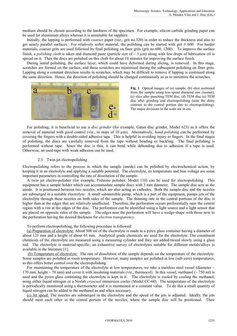
medium should be chosen according to the hardness of the specimen. For example, silicon carbide grinding paper can
be used for aluminium alloys whereas it is unsuitable for sapphire.
Initially, the lapping is performed with coarser paper (viz., grit no.320) in order to reduce the thickness and also to
get nearly parallel surfaces. For relatively softer material, the polishing can be started with grit # 600. For harder
materials, coarser grits are used followed by final polishing on finer grits (grit no.600, 1200). To improve the surface
finish, a polishing cloth is taken and diamond paste (particle size of ~ 3 µm) along with few drops of lubrication oil is
spread on it. Then the discs are polished on this cloth for about 10 minutes for improving the surface finish.
During initial polishing, the surface layer, which could have deformed during slicing, is removed. In this stage,
scratches are formed on the surface, and these scratches are minimised during the subsequent polishing on finer grits.
Lapping along a constant direction results in scratches, which may be difficult to remove if lapping is continued along
the same direction. Hence, the direction of polishing should be changed continuously so as to minimize the scratches.
Fig. 1 Optical images of (a) sample, (b) slice sectioned
from the sample using low-speed diamond saw (isomet),
(c) slice after punching TEM disc, (d) TEM disc (e) TEM
disc after grinding and electropolishing (note the shiny
contrast in the central portion due to electropolishing).
The major divisions in the scale are in cm.
For polishing, it is beneficial to use a disc grinder (for example, Gatan disc grinder, Model 623) as it offers the
removal of material with good control (viz., in steps of 10 µm). Alternatively, hand polishing can be performed by
covering the fingers with a double-sided adhesive tape. This is helpful in avoiding injury to fingers. In the final stages
of polishing, the discs are carefully removed from the tape without bending or buckling. The final polishing is
performed without tape. Since the disc is thin, it can bend while debonding due to adhesion if a tape is used.
Otherwise, an used-tape with weak adhesion can be used.
2.3 Twin-jet electropolishing
Electropolishing refers to the process in which the sample (anode) can be polished by electrochemical action, by
keeping it in an electrolyte and applying a suitable potential. The electrolyte, its temperature and bias voltage are some
important parameters in controlling the rate of dissolution of the sample.
A twin jet electro-polisher (for example, Fishione polisher, Model 110) can be used for electropolishing. This
equipment has a sample holder which can accommodate sample discs with 3 mm diameter. The sample disc acts as the
anode. It is positioned between two nozzles, which are also acting as cathodes. Both the sample disc and the nozzles
are submerged in a suitable electrolyte. A small submersible pump, which is a part of the equipment, pumps jets of the
electrolyte through these nozzles on both sides of the sample. The thinning rate in the central portions of the disc is
higher than at the edges that are relatively unaffected. Therefore, the perforation occurs preferentially near the central
region with a rim at the edges of the disc. The perforation can be identified using a light source and a light sensor that
are placed on opposite sides of the sample. The edges near the perforation will have a wedge-shape with those next to
the perforation having the desired thickness for electron transparency.
To perform electropolishing, the following procedure is followed:
(a) Preparation of electrolyte: About 500 ml of the electrolyte is made in a pyrex glass container having a diameter of
about 125 mm and a height of about 65 mm. Analytical grade chemicals are used for the electrolyte. The constituent
chemicals of the electrolyte are measured using a measuring cylinder and they are added/mixed slowly using a glass
rod. The electrolyte is material-specific; an exhaustive survey of electrolytes suitable for different metals/alloys is
available in the literature [1].
(b) Temperature of electrolyte: The rate of dissolution of the sample depends on the temperature of the electrolyte.
Some samples are polished at room temperature. However, many samples are polished at low (sub-zero) temperatures,
as this offers better control over the electropolishing.
For maintaining the temperature of the electrolyte at low temperatures, we take a stainless steel vessel (diameter ~
170 mm, height ~ 70 mm) and cover it with insulating materials (viz., thermocol). In this vessel, methanol (~ 750 ml) is
used and the pyrex glass containing the electrolyte is kept in it. The electrolyte is cooled by cooling the methanol,
using either liquid nitrogen or a Neslab cryocool immersion cooler (Model CC-60). The temperature of the electrolyte
is periodically monitored using a thermometer and it is maintained at a constant value. To do this a small quantity of
liquid nitrogen can be added to the methanol as and when necessary.
(c) Jet speed: The nozzles are submerged in the electrolyte and the speed of the jets is adjusted. Ideally, the jets
should meet each other in the central portion of the nozzles, where the sample disc will be positioned. Their
Microscopy: Science, Technology, Applications and Education A. Méndez-Vilas and J. Díaz (Eds.)
©FORMATEX 2010 1233
______________________________________________
intersection should appear with a shape close to a bubble. Also, they should not result in turbulence in the electrolyte.
The jet speed should be set up keeping these features in mind.
(d) Specimen holder: The disc prepared as described in §2.2 is loaded in the sample holder. It acts as the anode. It is
kept between the nozzles in the electrolyte. The geometry of the electropolishing cell is such that the sample is also
positioned between a light source and a photodetector that are used for identification of the perforation.
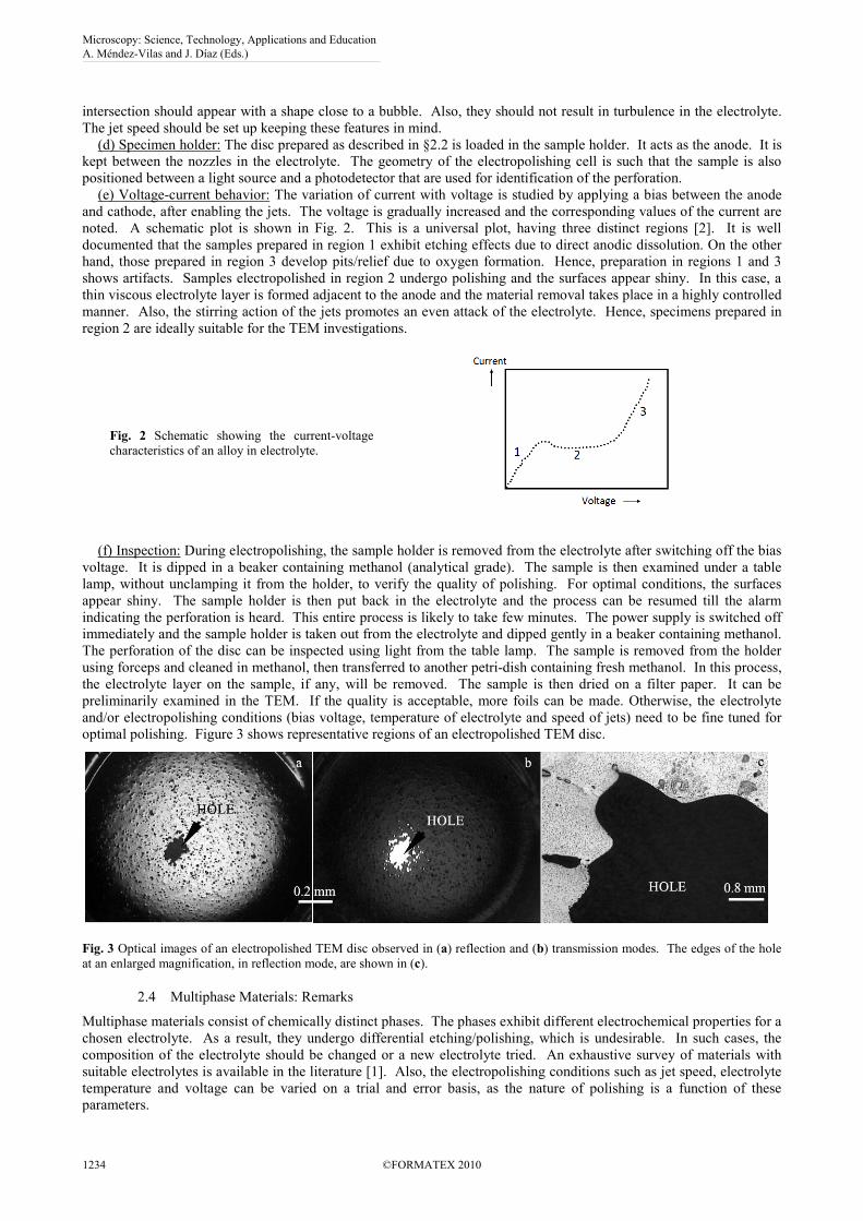
(e) Voltage-current behavior: The variation of current with voltage is studied by applying a bias between the anode
and cathode, after enabling the jets. The voltage is gradually increased and the corresponding values of the current are
noted. A schematic plot is shown in Fig. 2. This is a universal plot, having three distinct regions [2]. It is well
documented that the samples prepared in region 1 exhibit etching effects due to direct anodic dissolution. On the other
hand, those prepared in region 3 develop pits/relief due to oxygen formation. Hence, preparation in regions 1 and 3
shows artifacts. Samples electropolished in region 2 undergo polishing and the surfaces appear shiny. In this case, a
thin viscous electrolyte layer is formed adjacent to the anode and the material removal takes place in a highly controlled
manner. Also, the stirring action of the jets promotes an even attack of the electrolyte. Hence, specimens prepared in
region 2 are ideally suitable for the TEM investigations.
(f) Inspection: During electropolishing, the sample holder is removed from the electrolyte after switching off the bias
voltage. It is dipped in a beaker containing methanol (analytical grade). The sample is then examined under a table
lamp, without unclamping it from the holder, to verify the quality of polishing. For optimal conditions, the surfaces
appear shiny. The sample holder is then put back in the electrolyte and the process can be resumed till the alarm
indicating the perforation is heard. This entire process is likely to take few minutes. The power supply is switched off
immediately and the sample holder is taken out from the electrolyte and dipped gently in a beaker containing methanol.
The perforation of the disc can be inspected using light from the table lamp. The sample is removed from the holder
using forceps and cleaned in methanol, then transferred to another petri-dish containing fresh methanol. In this process,
the electrolyte layer on the sample, if any, will be removed. The sample is then dried on a filter paper. It can be
preliminarily examined in the TEM. If the quality is acceptable, more foils can be made. Otherwise, the electrolyte
and/or electropolishing conditions (bias voltage, temperature of electrolyte and speed of jets) need to be fine tuned for
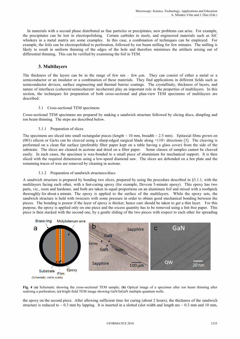
optimal polishing. Figure 3 shows representative regions of an electropolished TEM disc.
Fig. 3 Optical images of an electropolished TEM disc observed in (a) reflection and (b) transmission modes. The edges of the hole
at an enlarged magnification, in reflection mode, are shown in (c).
2.4 Multiphase Materials: Remarks
Multiphase materials consist of chemically distinct phases. The phases exhibit different electrochemical properties for a
chosen electrolyte. As a result, they undergo differential etching/polishing, which is undesirable. In such cases, the
composition of the electrolyte should be changed or a new electrolyte tried. An exhaustive survey of materials with
suitable electrolytes is available in the literature [1]. Also, the electropolishing conditions such as jet speed, electrolyte
temperature and voltage can be varied on a trial and error basis, as the nature of polishing is a function of these
parameters.
Fig. 2 Schematic showing the current-voltage
characteristics of an alloy in electrolyte.
Microscopy: Science, Technology, Applications and Education A. Méndez-Vilas and J. Díaz (Eds.)
1234 ©FORMATEX 2010
______________________________________________
In materials with a second phase distributed as fine particles or precipitates, new problems can arise. For example,
the precipitates can be lost in electropolishing. Certain carbides in steels, and engineered materials such as SiC
whiskers in a metal matrix are some examples. In this case, a combination of techniques can be employed. For
example, the foils can be electropolished to perforation, followed by ion beam milling for few minutes. The milling is
likely to result in uniform thinning of the edges of the hole and therefore minimises the artifacts arising out of
differential thinning. This can be verified by examining the foil in TEM.
3. Multilayers
The thickness of the layers can be in the range of few nm – few µm. They can consist of either a metal or a
semiconductor or an insulator or a combination of these materials. They find applications in different fields such as
semiconductor devices, surface engineering and thermal barrier coatings. The crystallinity, thickness of layers, and
nature of interfaces (coherent/semicoherent/ incoherent) play an important role in the properties of multilayers. In this
section, the techniques for preparation of both cross-sectional and plan-view TEM specimens of multilayers are
described:
3.1 Cross-sectional TEM specimens
Cross-sectional TEM specimens are prepared by making a sandwich structure followed by slicing discs, dimpling and
ion beam thinning. The steps are described below.
3.1.1 Preparation of slices
The specimens are sliced into small rectangular pieces (length ~ 10 mm, breadth ~ 2.5 mm). Epitaxial films grown on
(001) silicon or GaAs can be cleaved using a sharp-edged surgical blade along <110> directions [3]. The cleaving is
performed on a clean flat surface (preferably filter paper kept on a table having a glass cover) from the side of the
substrate. The slices are cleaned in acetone and dried on a filter paper. Some classes of samples cannot be cleaved
easily. In such cases, the specimen is wax-bonded to a small piece of aluminium for mechanical support. It is then
sliced with the required dimensions using a low-speed diamond saw. The slices are debonded on a hot plate and the
remaining traces of wax are removed by cleaning in acetone.
3.1.2 Preparation of sandwich structures/discs
A sandwich structure is prepared by bonding two slices, prepared by using the procedure described in §3.1.1, with the
multilayers facing each other, with a fast-curing epoxy (for example, Devcon 5-minute epoxy). This epoxy has two
parts, viz., resin and hardener, and both are taken in equal proportions on an aluminum foil and mixed with a toothpick
thoroughly for about a minute. The epoxy is applied to the surface of the multilayers. While the epoxy sets, the
sandwich structure is held with tweezers with some pressure in order to obtain good mechanical bonding between the
pieces. The bonding is poorer if the layer of epoxy is thicker; hence care should be taken to get a thin layer. For this
purpose, the epoxy is applied only on one piece and the excess quantity has to be removed using a lint-free paper. This
piece is then stacked with the second one, by a gentle sliding of the two pieces with respect to each other for spreading
the epoxy on the second piece. After allowing sufficient time for curing (about 2 hours), the thickness of the sandwich
structure is reduced to ~ 0.3 mm by lapping. It is inserted in a slotted (slot width and length are ~ 0.3 mm and 10 mm,
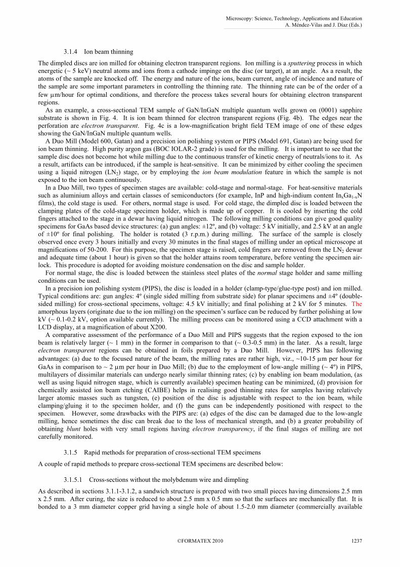
Fig. 4 (a) Schematic showing the cross-sectional TEM sample; (b) Optical image of a specimen after ion beam thinning after
realising a perforation; (c) bright field TEM image showing GaN/InGaN multiple quantum wells.
Microscopy: Science, Technology, Applications and Education A. Méndez-Vilas and J. Díaz (Eds.)
©FORMATEX 2010 1235
______________________________________________
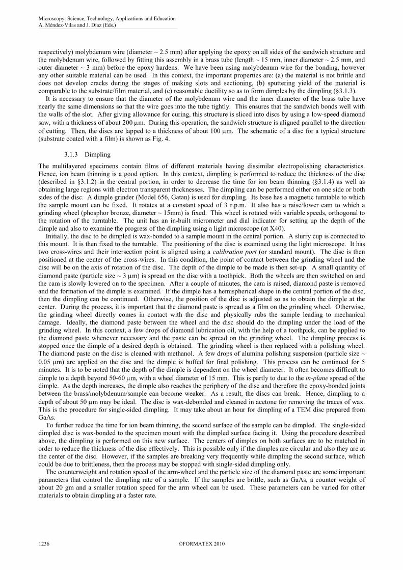
respectively) molybdenum wire (diameter ~ 2.5 mm) after applying the epoxy on all sides of the sandwich structure and
the molybdenum wire, followed by fitting this assembly in a brass tube (length ~ 15 mm, inner diameter ~ 2.5 mm, and
outer diameter ~ 3 mm) before the epoxy hardens. We have been using molybdenum wire for the bonding, however
any other suitable material can be used. In this context, the important properties are: (a) the material is not brittle and
does not develop cracks during the stages of making slots and sectioning, (b) sputtering yield of the material is
comparable to the substrate/film material, and (c) reasonable ductility so as to form dimples by the dimpling (§3.1.3).
It is necessary to ensure that the diameter of the molybdenum wire and the inner diameter of the brass tube have
nearly the same dimensions so that the wire goes into the tube tightly. This ensures that the sandwich bonds well with
the walls of the slot. After giving allowance for curing, this structure is sliced into discs by using a low-speed diamond
saw, with a thickness of about 200 µm. During this operation, the sandwich structure is aligned parallel to the direction
of cutting. Then, the discs are lapped to a thickness of about 100 µm. The schematic of a disc for a typical structure
(substrate coated with a film) is shown as Fig. 4.
3.1.3 Dimpling
The multilayered specimens contain films of different materials having dissimilar electropolishing characteristics.
Hence, ion beam thinning is a good option. In this context, dimpling is performed to reduce the thickness of the disc
(described in §3.1.2) in the central portion, in order to decrease the time for ion beam thinning (§3.1.4) as well as
obtaining large regions with electron transparent thicknesses. The dimpling can be performed either on one side or both
sides of the disc. A dimple grinder (Model 656, Gatan) is used for dimpling. Its base has a magnetic turntable to which
the sample mount can be fixed. It rotates at a constant speed of 3 r.p.m. It also has a raise/lower cam to which a
grinding wheel (phosphor bronze, diameter ~ 15mm) is fixed. This wheel is rotated with variable speeds, orthogonal to
the rotation of the turntable. The unit has an in-built micrometer and dial indicator for setting up the depth of the
dimple and also to examine the progress of the dimpling using a light microscope (at X40).
Initially, the disc to be dimpled is wax-bonded to a sample mount in the central portion. A slurry cup is connected to
this mount. It is then fixed to the turntable. The positioning of the disc is examined using the light microscope. It has
two cross-wires and their intersection point is aligned using a calibration port (or standard mount). The disc is then
positioned at the center of the cross-wires. In this condition, the point of contact between the grinding wheel and the
disc will be on the axis of rotation of the disc. The depth of the dimple to be made is then set-up. A small quantity of
diamond paste (particle size ~ 3 µm) is spread on the disc with a toothpick. Both the wheels are then switched on and
the cam is slowly lowered on to the specimen. After a couple of minutes, the cam is raised, diamond paste is removed
and the formation of the dimple is examined. If the dimple has a hemispherical shape in the central portion of the disc,
then the dimpling can be continued. Otherwise, the position of the disc is adjusted so as to obtain the dimple at the
center. During the process, it is important that the diamond paste is spread as a film on the grinding wheel. Otherwise,
the grinding wheel directly comes in contact with the disc and physically rubs the sample leading to mechanical
damage. Ideally, the diamond paste between the wheel and the disc should do the dimpling under the load of the
grinding wheel. In this context, a few drops of diamond lubrication oil, with the help of a toothpick, can be applied to
the diamond paste whenever necessary and the paste can be spread on the grinding wheel. The dimpling process is
stopped once the dimple of a desired depth is obtained. The grinding wheel is then replaced with a polishing wheel.
The diamond paste on the disc is cleaned with methanol. A few drops of alumina polishing suspension (particle size ~
0.05 µm) are applied on the disc and the dimple is buffed for final polishing. This process can be continued for 5
minutes. It is to be noted that the depth of the dimple is dependent on the wheel diameter. It often becomes difficult to
dimple to a depth beyond 50-60 µm, with a wheel diameter of 15 mm. This is partly to due to the in-plane spread of the
dimple. As the depth increases, the dimple also reaches the periphery of the disc and therefore the epoxy-bonded joints
between the brass/molybdenum/sample can become weaker. As a result, the discs can break. Hence, dimpling to a
depth of about 50 µm may be ideal. The disc is wax-debonded and cleaned in acetone for removing the traces of wax.
This is the procedure for single-sided dimpling. It may take about an hour for dimpling of a TEM disc prepared from
GaAs.
To further reduce the time for ion beam thinning, the second surface of the sample can be dimpled. The single-sided
dimpled disc is wax-bonded to the specimen mount with the dimpled surface facing it. Using the procedure described
above, the dimpling is performed on this new surface. The centers of dimples on both surfaces are to be matched in
order to reduce the thickness of the disc effectively. This is possible only if the dimples are circular and also they are at
the center of the disc. However, if the samples are breaking very frequently while dimpling the second surface, which
could be due to brittleness, then the process may be stopped with single-sided dimpling only.
The counterweight and rotation speed of the arm-wheel and the particle size of the diamond paste are some important
parameters that control the dimpling rate of a sample. If the samples are brittle, such as GaAs, a counter weight of
about 20 gm and a smaller rotation speed for the arm wheel can be used. These parameters can be varied for other
materials to obtain dimpling at a faster rate.
Microscopy: Science, Technology, Applications and Education A. Méndez-Vilas and J. Díaz (Eds.)
1236 ©FORMATEX 2010
______________________________________________
3.1.4 Ion beam thinning
The dimpled discs are ion milled for obtaining electron transparent regions. Ion milling is a sputtering process in which
energetic (~ 5 keV) neutral atoms and ions from a cathode impinge on the disc (or target), at an angle. As a result, the
atoms of the sample are knocked off. The energy and nature of the ions, beam current, angle of incidence and nature of
the sample are some important parameters in controlling the thinning rate. The thinning rate can be of the order of a
few µm/hour for optimal conditions, and therefore the process takes several hours for obtaining electron transparent
regions.
As an example, a cross-sectional TEM sample of GaN/InGaN multiple quantum wells grown on (0001) sapphire
substrate is shown in Fig. 4. It is ion beam thinned for electron transparent regions (Fig. 4b). The edges near the
perforation are electron transparent. Fig. 4c is a low-magnification bright field TEM image of one of these edges
showing the GaN/InGaN multiple quantum wells.
A Duo Mill (Model 600, Gatan) and a precision ion polishing system or PIPS (Model 691, Gatan) are being used for
ion beam thinning. High purity argon gas (BOC IOLAR-2 grade) is used for the milling. It is important to see that the
sample disc does not become hot while milling due to the continuous transfer of kinetic energy of neutrals/ions to it. As
a result, artifacts can be introduced, if the sample is heat-sensitive. It can be minimized by either cooling the specimen
using a liquid nitrogen (LN2) stage, or by employing the ion beam modulation feature in which the sample is not
exposed to the ion beam continuously.
In a Duo Mill, two types of specimen stages are available: cold-stage and normal-stage. For heat-sensitive materials
such as aluminium alloys and certain classes of semiconductors (for example, InP and high-indium content InxGa1-xN
films), the cold stage is used. For others, normal stage is used. For cold stage, the dimpled disc is loaded between the
clamping plates of the cold-stage specimen holder, which is made up of copper. It is cooled by inserting the cold
fingers attached to the stage in a dewar having liquid nitrogen. The following milling conditions can give good quality
specimens for GaAs based device structures: (a) gun angles: ±12º, and (b) voltage: 5 kV initially, and 2.5 kV at an angle
of ±10º for final polishing. The holder is rotated (3 r.p.m.) during milling. The surface of the sample is closely
observed once every 3 hours initially and every 30 minutes in the final stages of milling under an optical microscope at
magnifications of 50-200. For this purpose, the specimen stage is raised, cold fingers are removed from the LN2 dewar
and adequate time (about 1 hour) is given so that the holder attains room temperature, before venting the specimen air-
lock. This procedure is adopted for avoiding moisture condensation on the disc and sample holder.
For normal stage, the disc is loaded between the stainless steel plates of the normal stage holder and same milling
conditions can be used.
In a precision ion polishing system (PIPS), the disc is loaded in a holder (clamp-type/glue-type post) and ion milled.
Typical conditions are: gun angles: 4º (single sided milling from substrate side) for planar specimens and ±4º (double-
sided milling) for cross-sectional specimens, voltage: 4.5 kV initially; and final polishing at 2 kV for 5 minutes. The
amorphous layers (originate due to the ion milling) on the specimen’s surface can be reduced by further polishing at low
kV (~ 0.1-0.2 kV, option available currently). The milling process can be monitored using a CCD attachment with a
LCD display, at a magnification of about X200.
A comparative assessment of the performance of a Duo Mill and PIPS suggests that the region exposed to the ion
beam is relatively larger (~ 1 mm) in the former in comparison to that (~ 0.3-0.5 mm) in the later. As a result, large
electron transparent regions can be obtained in foils prepared by a Duo Mill. However, PIPS has following
advantages: (a) due to the focused nature of the beam, the milling rates are rather high, viz., ~10-15 µm per hour for
GaAs in comparison to ~ 2 µm per hour in Duo Mill; (b) due to the employment of low-angle milling (~ 4º) in PIPS,
multilayers of dissimilar materials can undergo nearly similar thinning rates; (c) by enabling ion beam modulation, (as
well as using liquid nitrogen stage, which is currently available) specimen heating can be minimized, (d) provision for
chemically assisted ion beam etching (CAIBE) helps in realising good thinning rates for samples having relatively
larger atomic masses such as tungsten, (e) position of the disc is adjustable with respect to the ion beam, while
clamping/gluing it to the specimen holder, and (f) the guns can be independently positioned with respect to the
specimen. However, some drawbacks with the PIPS are: (a) edges of the disc can be damaged due to the low-angle
milling, hence sometimes the disc can break due to the loss of mechanical strength, and (b) a greater probability of
obtaining blunt holes with very small regions having electron transparency, if the final stages of milling are not
carefully monitored.
3.1.5 Rapid methods for preparation of cross-sectional TEM specimens
A couple of rapid methods to prepare cross-sectional TEM specimens are described below:
3.1.5.1 Cross-sections without the molybdenum wire and dimpling
As described in sections 3.1.1-3.1.2, a sandwich structure is prepared with two small pieces having dimensions 2.5 mm
x 2.5 mm. After curing, the size is reduced to about 2.5 mm x 0.5 mm so that the surfaces are mechanically flat. It is
bonded to a 3 mm diameter copper grid having a single hole of about 1.5-2.0 mm diameter (commercially available
Microscopy: Science, Technology, Applications and Education A. Méndez-Vilas and J. Díaz (Eds.)
©FORMATEX 2010 1237
______________________________________________
from Agar). Then, it is mechanically reduced to a thickness of about 25-30 µm by very careful grinding using diamond
lapping films, in steps of particle sizes of ~15, 6, 3, 1, 0.5 µm. For the grinding and polishing, a disc grinder is helpful.
Also, it is good to keep small pieces of silicon around this copper grid for minimising the edge-rounding of the
sandwich structure and copper grid. This is very important for reducing the specimen thickness below ~ 75 µm. Then,
this specimen is subjected to ion-beam thinning directly without the necessity of dimpling.
The small-angle cleavage technique also permits rapid preparation of TEM specimens. However it is suitable for
materials which can undergo cleaving readily (for example, GaAs, Silicon). For more details, refer [4].
3.1.5.2 Cross-sections of several specimens
It is often necessary to rapidly prepare cross-sections of several samples. In this case, small pieces with dimensions of
about 2.5 mm x 2.5 mm were cut from the samples. They were wax-bonded to a glass slide (film is facing the glass
surface) and the substrate’s side is polished so that the thickness of the specimen is about 40-50 µm. Then, they were
carefully debonded and cleaned in acetone, and bonded together along the cross-section (unlike the previous case in
which the film is bonded to the film in the sandwich structure, the film is bonded to the substrate in this case) on a 3
mm diameter copper grid having a single hole of about 2.0 mm diameter. This way, about five specimens can be
mounted on a single grid. The rest of the hole of the TEM grid can be covered with same material. Then, by careful
grinding using diamond lapping films, a thickness of about 25-30 µm is realised. It is subjected to ion-beam milling
using single modulation so that the milling takes place from the substrate side. The gun angles may be kept at ±3˚.
This way, several samples can be prepared at a time [5]. However, this method may not be very useful for very hard
materials, such as structures having (0001) sapphire as a substrate.
3.1.6 Remarks on mechanical polishing/ion-milling of cross-sectional TEM specimens
Semiconductor samples are brittle; hence they can develop cracks during lapping/dimpling. As a result, the samples can
break or small pieces can be chipped-off from the sample. If the breakages are many in the central portion of the TEM
disc, the ion beam milling cannot be effective. Further, if the epoxy layer is thick, then the epoxy bonding between the
molybdenum wire, brass tube and the sandwich structure will not be strong and the bonding can fail during grinding.
Hence, careful attention is required at all levels. Other important suggestions are: (a) using a disc grinder for the
grinding, (b) washing the grinding paper at regular intervals so that the debris (originating from the grinding) are
removed, (c) keeping small pieces of silicon around the copper grid during polishing so that edge-rounding effects are
minimised, (d) employing ion beam modulation for heat sensitive materials, (e) protecting the glue line of the specimen
as well as the clamp-type holder by double beam modulation.
3.2 Plan-view TEM specimens
TEM discs are punched from the sample using an ultrasonic disc cutter (for example, Model 601, Gatan). For this
purpose, the slices are wax-bonded to a glass slide with the coatings facing it. The glass slide is then wax-bonded to the
specimen table of the disc cutter. The slice is positioned below the tubular cutting tool. A small quantity (1/4 of a tea
spoon) of silicon carbide grit is kept on the sample with a spatula, and slurry is made with water. A syringe filled with
water is connected to the equipment and water is flushed gently through the cutting tool. Against this water pressure,
the equipment is switched on and the cutting tool is lowered on to the sample. The cutting tool vibrates ultrasonically
against the sample due to the action of a piezoelectric crystal on it. As a result, the particles in the grit slurry impact the
sample and erode it with a circular impression, which slowly develops as a cut. The design of this equipment is such
that the sample is pressed against the tool head through a spring-loaded action of the sample holder. The progress of the
cutting can be monitored through a dial gauge. It is important to keep the adequate water pressure through the syringe.
Otherwise, the slurry can enter the cutting tool and block the ultrasonic waves. In general, a gentle thumb pressure on
the syringe is satisfactory for this operation. Also, the cutting tool should be pressed against the sample gently;
otherwise, the sample can break. Sometimes, the discs can be trapped in the bore of the cutting tool. They should be
removed gently by either tapping or flushing with water using a syringe. The discs obtained will have both glass and
the sample with wax bonding between them. They can be debonded on a hot plate followed by cleaning in acetone.
The samples are then lapped from the substrate-side using a disc polisher and the thickness is reduced to about 100 µm.
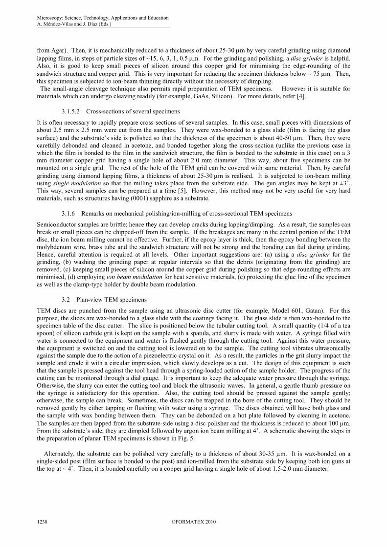
From the substrate’s side, they are dimpled followed by argon ion beam milling at 4˚. A schematic showing the steps in
the preparation of planar TEM specimens is shown in Fig. 5.
Alternately, the substrate can be polished very carefully to a thickness of about 30-35 µm. It is wax-bonded on a
single-sided post (film surface is bonded to the post) and ion-milled from the substrate side by keeping both ion guns at
the top at ~ 4˚. Then, it is bonded carefully on a copper grid having a single hole of about 1.5-2.0 mm diameter.
Microscopy: Science, Technology, Applications and Education A. Méndez-Vilas and J. Díaz (Eds.)
1238 ©FORMATEX 2010
______________________________________________
3.3 Wedge polishing
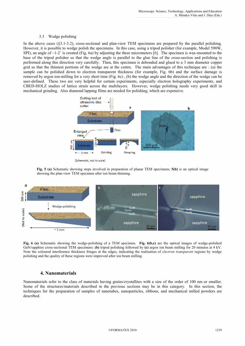
In the above cases (§3.1-3.2), cross-sectional and plan-view TEM specimens are prepared by the parallel polishing.
However, it is possible to wedge polish the specimens. In this case, using a tripod polisher (for example, Model 590W,
SPI), an angle of ~1-2˚ is created (Fig. 6a) by adjusting the three micrometers [6]. The specimen is wax-mounted to the
base of the tripod polisher so that the wedge angle is parallel to the glue line of the cross-section and polishing is
performed along this direction very carefully. Then, this specimen is debonded and glued to a 3 mm diameter copper
grid so that the thinnest portions of the wedge are at the centre. The main advantages of this technique are : (a) the
sample can be polished down to electron transparent thickness (for example, Fig. 6b) and the surface damage is
removed by argon ion-milling for a very short time (Fig. 6c) , (b) the wedge angle and the direction of the wedge can be
user-defined. These two are very helpful for certain experiments, especially electron holography experiments, and
CBED-HOLZ studies of lattice strain across the multilayers. However, wedge polishing needs very good skill in
mechanical grinding. Also diamond lapping films are needed for polishing, which are expensive.
Fig. 6 (a) Schematic showing the wedge-polishing of a TEM specimen. Fig. 6(b,c) are the optical images of wedge-polished
GaN/sapphire cross-sectional TEM specimens: (b) tripod polishing followed by (c) argon ion beam milling for 20 minutes at 4 kV.
Note the coloured interference thickness fringes at the edges, indicating the realisation of electron transparent regions by wedge
polishing and the quality of these regions were improved after ion beam milling.
4. Nanomaterials
Nanomaterials refer to the class of materials having grains/crystallites with a size of the order of 100 nm or smaller.
Some of the structures/materials described in the previous sections may be in this category. In this section, the
techniques for the preparation of samples of nanotubes, nanoparticles, ribbons, and mechanical milled powders are
described.
Fig. 5 (a) Schematic showing steps involved in preparation of planar TEM specimens; 5(b) is an optical image
showing the plan-view TEM specimen after ion beam thinning.
Microscopy: Science, Technology, Applications and Education A. Méndez-Vilas and J. Díaz (Eds.)
©FORMATEX 2010 1239
______________________________________________
4.1 Nanoparticles with non-magnetic nature
The sample (nanoparticles) is dispersed in a solution using ultrasonication for five minutes. The solution used (a)
should be chemically inert, (b) should not result in agglomeration of the nanoparticles, (c) should not leave carbon
residues, and (d) should evaporate in a reasonable time frame (let us say 10-20 minutes) at room temperature. A simple
method of examining whether the solution leaves carbon residues or not is to keep a couple of drops on a clean glass
slide and observe after evaporation; if the glass slide is not clear, then the solution may not be useful! Hexane is a
suitable medium; if not available, methanol can be tried. The suspended particles are lifted on a carbon-coated copper
grid (# 200 or 300 mesh) (for example, Fig. 7a) or holey carbon grid, with the help of forceps, by dipping the grid in the
beaker gently and withdrawing horizontally. The grid is dried on a filter paper under an infrared lamp, followed by
inspection in the TEM. The exercise can be repeated until a satisfactory collection is obtained.
In the case of nanoparticles prepared by deposition techniques, sometimes it may become difficult to transfer them to
the carbon coated grids. In such cases, if the effect of the substrate is insignificant on their formation, they can be
directly coated on a KCl substrate as a thin film with a thickness of the order of 100 nm. If the film size is larger, it can
be cut into small portions (about 2 mm x 2 mm) with a sharp blade gently without breaking the substrate. The substrate
is then dissolved in water and one of the pieces of the floating films is lifted on a carbon-coated TEM grid. It is dried
under an infrared lamp. Alternatively, the nanoparticles can be coated on a carbon-coated TEM grid directly.
4.2 Nanoparticles with magnetic nature
The preparation of TEM samples of magnetic powders is difficult due to following reasons. Firstly, the magnetic
particles exhibit agglomeration. They can be dispersed in a solution by ultrasonication, however they readily get
agglomerated as soon as the sonification is stopped. These agglomerates are unsuitable for TEM investigations.
Secondly, for microstructural studies, the sample is placed between pole pieces of the objective lens of the TEM. These
pole pieces are electromagnets (exception is having electrostatic lenses), as they are made up of soft magnetic material
and carry large excitation currents. As a result, the particles get magnetized. This has the following effects: (a) the
particles can be attracted by the pole pieces, (b) the particles can exhibit drift under electron beam, hence are unsuitable
for high-resolution studies, and (c) the pole pieces can be contaminated with the particles over a period of time. Due to
these reasons, it is necessary to embed the particles in a medium, which is stable under an electron beam for TEM
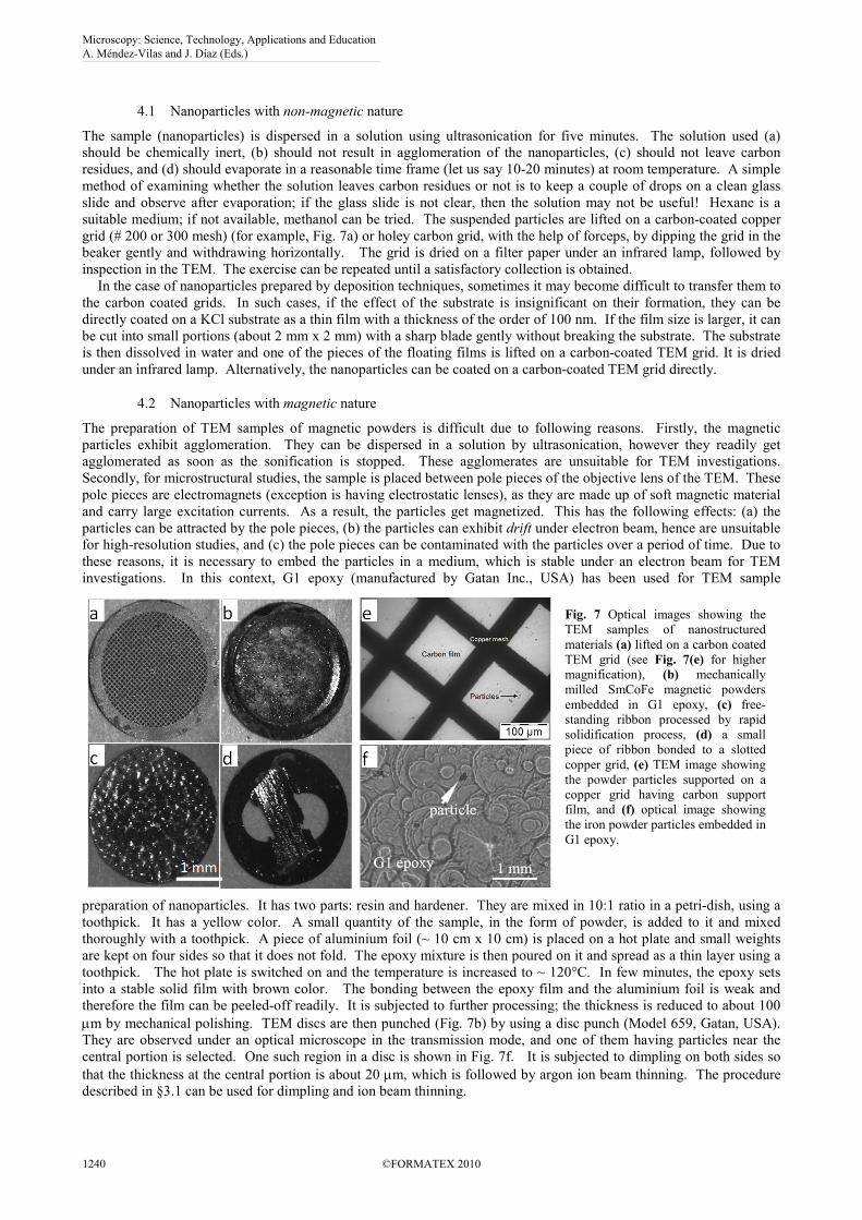
investigations. In this context, G1 epoxy (manufactured by Gatan Inc., USA) has been used for TEM sample
preparation of nanoparticles. It has two parts: resin and hardener. They are mixed in 10:1 ratio in a petri-dish, using a
toothpick. It has a yellow color. A small quantity of the sample, in the form of powder, is added to it and mixed
thoroughly with a toothpick. A piece of aluminium foil (~ 10 cm x 10 cm) is placed on a hot plate and small weights
are kept on four sides so that it does not fold. The epoxy mixture is then poured on it and spread as a thin layer using a
toothpick. The hot plate is switched on and the temperature is increased to ~ 120°C. In few minutes, the epoxy sets
into a stable solid film with brown color. The bonding between the epoxy film and the aluminium foil is weak and
therefore the film can be peeled-off readily. It is subjected to further processing; the thickness is reduced to about 100
µm by mechanical polishing. TEM discs are then punched (Fig. 7b) by using a disc punch (Model 659, Gatan, USA).
They are observed under an optical microscope in the transmission mode, and one of them having particles near the
central portion is selected. One such region in a disc is shown in Fig. 7f. It is subjected to dimpling on both sides so
that the thickness at the central portion is about 20 µm, which is followed by argon ion beam thinning. The procedure
described in §3.1 can be used for dimpling and ion beam thinning.
Fig. 7 Optical images showing the
TEM samples of nanostructured
materials (a) lifted on a carbon coated
TEM grid (see Fig. 7(e) for higher
magnification), (b) mechanically
milled SmCoFe magnetic powders
embedded in G1 epoxy, (c) free-
standing ribbon processed by rapid
solidification process, (d) a small
piece of ribbon bonded to a slotted
copper grid, (e) TEM image showing
the powder particles supported on a
copper grid having carbon support
film, and (f) optical image showing
the iron powder particles embedded in
G1 epoxy.
Microscopy: Science, Technology, Applications and Education A. Méndez-Vilas and J. Díaz (Eds.)
1240 ©FORMATEX 2010
______________________________________________
4.3 Ribbons
Ribbons prepared by a rapid solidification process generally have a thickness of the order of 50 µm. TEM discs are
punched from them using a disc-punch (Model 659, Gatan, USA). They are polished for a smooth surface. They can
be handled directly if they have good mechanical strength (Fig. 7c). If they are brittle, they can be supported by
bonding them to 3 mm diameter slotted grids with Devcon 5-minute epoxy (Fig. 7d). The epoxy should not spread on
the surfaces of the sample while bonding. The samples can be either electropolished or ion beam thinned based on their
electrical conductivity.
For investigating the microstructure across the thickness of a ribbon, cross-sectional TEM specimens should be
prepared. In this case, a small piece of ribbon (length ~ 10 mm, width ~ 2.5 mm) can be used in place of the sandwich
structure described in §3.1, and the cross-sectional TEM foils can be prepared by argon ion beam thinning.
5. Composites
A composite consists of a matrix with reinforcements. The matrix can be either ceramic or polymer or metal/alloy. The
reinforcements can be either fibers, or whiskers or particulates. Some examples are SiC particulate reinforced
aluminium matrix composite, and silica fiber reinforced silica matrix composite.
To prepare TEM samples of composites, it is difficult to adopt electropolishing techniques due to: (a) etching rates of
the constituent phases may be different, especially the thinning rates of particulates/whiskers are significantly different
in comparison to the metal matrix, (b) certain classes of composites contain functional coatings between the
reinforcements and the matrix, and their interfaces are of interest for study, and (c) ceramics exhibit very high electrical
resistivity, hence they cannot be electropolished. Hence, ion beam thinning is a suitable method.
The preparation of TEM discs of a composite depends on its mechanical properties. Metal matrix composites are
likely to have some ductility. In such cases, the discs can be prepared by following the procedure described in §2 for
metals and alloys. If the composite is brittle, the discs can be punched by the ultrasonic disc cutter, followed by
lapping, double-sided dimpling and argon ion beam thinning.
Preparation of TEM foils of certain composites is difficult, as they cannot be cut to a disc shape. Also, they break
readily while polishing. One of the examples is a ceramic fiber reinforced ceramic matrix composite. In such cases, a
small piece of the sample can be mounted in the slotted molybdenum wire, and the discs can be prepared using the
procedure described for cross-sections of multilayers in §3.1.
6. Brittle materials
Some materials are brittle and can break into pieces at different stages of preparation of TEM samples. Samarium
cobalt can be placed in this category. TEM specimens of these materials can be prepared by following the procedure
described for cross-sections in §3.1. In this case, a small rectangular piece with dimensions of the order 10 mm x 0.3
mm x 2.5 mm is sliced from the sample using a low-speed diamond saw. It is used in place of the sandwich structure
shown in Fig. 4a. If there is a desired direction of observing the foil in the TEM, it should be considered at the stage of
slicing of sample. Considering the geometry of the disc preparation, the sample will be along the direction of length for
zero-tilt conditions in the TEM. Hence, the length of the rectangular piece should be along the direction of observation.
7. Site-specific TEM specimens by focused ion beam (FIB) milling
There is a great interest in the preparation of site-specific TEM specimens, for example, examining a particular region
of an integrated circuit, the microstructure of the crack tip in fracture and fatigue experiments and the deformation
around a nanoindentation. For these cases FIB is a very useful tool. Also, needle shaped specimens required for certain
tomography studies can be prepared with FIB.
A typical FIB uses a gallium ion beam, originating from a liquid metal ion source. This beam is accelerated (up to 30
kV) and rastered over the specimen’s surface so that site-specific milling of the specimen can be performed [7].
Modern FIBs (for example, FEI Helios) have dual-beam (both electron beam and ion beam) columns, gas-injection
systems (GIS) and an Omniprobe (or micromanipulator) which can be used for imaging and ion-beam sectioning of a
thin lamella and transfer/welding to the TEM grids.
The typical steps/conditions involved in preparing TEM specimens are: (a) identification of the region of interest, (b)
bringing the specimen to eucentric height, (c) platinum deposition using GIS (initially by the electron beam, then by the
gallium ion beam) with dimensions : length ~ 15 µm, breadth ~ 2 µm and thickness ~ 0.3-1.0 µm (the thickness can be
controlled by deposition time and dwell time) over this region, (d) ion milling (with gallium ions at ~30 kV) to make a
lamella by forming trenches adjacent to the platinum coated region using cleaning cross-section mode (used for FEI
FIBs) (Fig. 8a), (e) lift-out of the lamella using an Omniprobe, (f) transferring the lamella onto the TEM grid, and
Microscopy: Science, Technology, Applications and Education A. Méndez-Vilas and J. Díaz (Eds.)
©FORMATEX 2010 1241
______________________________________________
welding with platinum metal (Fig. 8b), and (g) cleaning the specimen’s surface with a low energy gallium beam (at 5
kV or lower) by tilting the milled surface of the specimen at ~ 1-2˚ with respect to the beam so that the final thickness
of the lamella ~ 150-200 nm.
The FIB offers rapid TEM specimen preparation, however it is necessary to note the following: (a) gallium ions are
heavier (atomic number of Ga : 21) and more energetic (~30 keV), than the argon ions used in PIPS (atomic number of
argon is 18 and the incident energy ~ 4-5 keV or lower), hence implantation damage of the lattice is higher than in
PIPS, (b) artifacts (such as droplets/curtaining effects on the milled surfaces) can appear, and (c) working with a low
energy (1-2 keV) gallium ion beam may not be user-friendly (due to instrumentation optics). Hence, cleaning the FIB
prepared specimen in a PIPS with low-energy argon ions (1-2 kV, ±3˚ gun angles, for a couple of minutes) using single
modulation mode of operation (milling from the side of the substrate) seems to be a good option (Fig. 9). In this
context, the specimen may be bonded perpendicular to the fingers of a copper TEM grid, as shown in Fig. 8b.
Although, both the ion beam and the electron beam can be used for imaging, the ion beam sputters the surface; hence
electron beam is preferred and snapshots can be taken with the ion beam as and when necessary. Also, for the platinum
deposition, the e-beam is suggested initially, followed by the ion-beam (as shown in Fig.9). A careful bonding of the
lift-out lamella to the copper grid with platinum is also important, otherwise, the lamella can be lost during
handling/cleaning in the PIPS. In this context, the following studies are needed: (a) the relative content of platinum in
the platinum deposition layer as a function of the energy of the incident electron beam and the electron source (FEG
versus thermionic), and (b) the bond strength of platinum deposited on the copper grid in the respective cases.
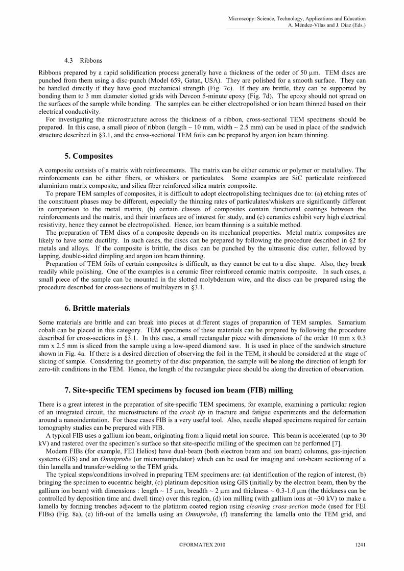
Fig. 8 FIB preparation of TEM specimens: (a) thin lamella prepared by gallium ion milling, (b) thin lamella platinum-bonded to the
TEM grid using an omniprobe after lift-off, (c) TEM specimen along cross-section, and (d) plan-view.
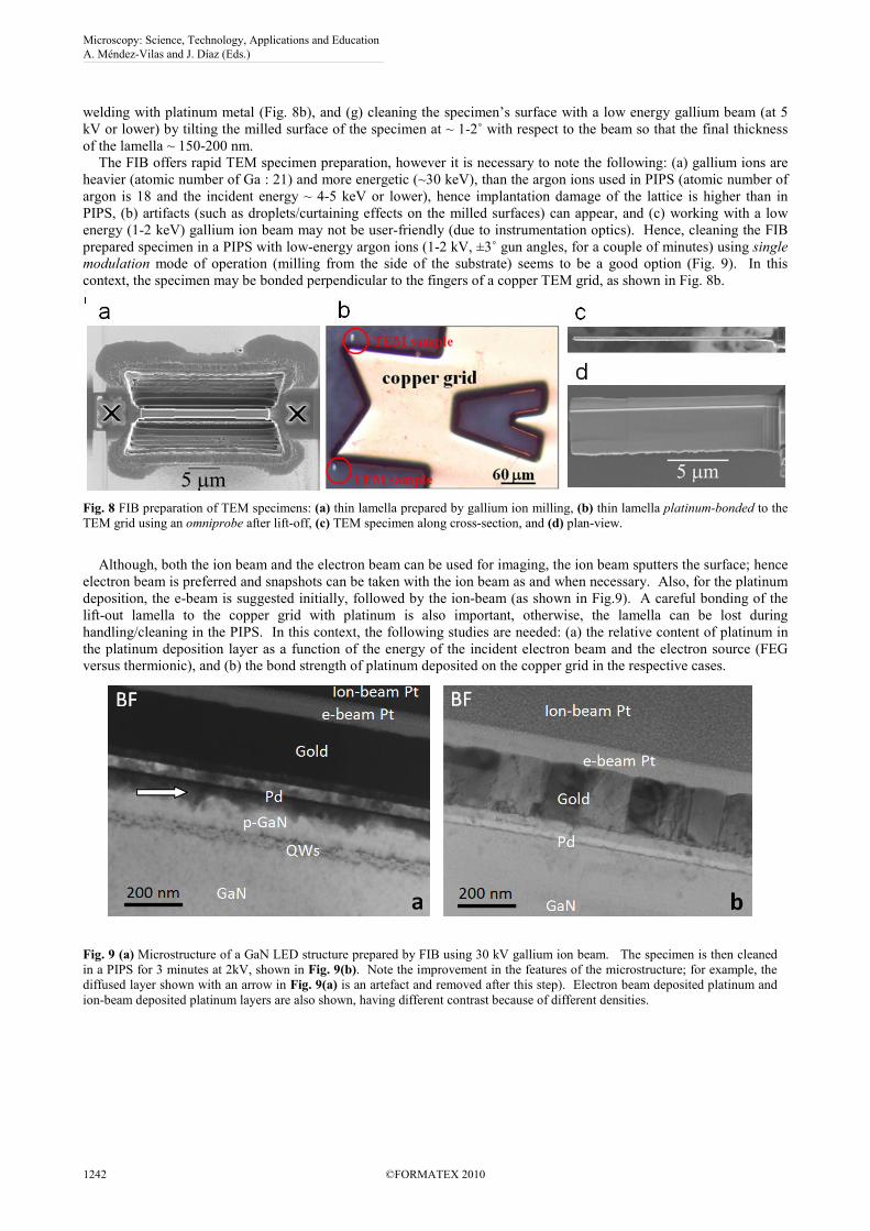
Fig. 9 (a) Microstructure of a GaN LED structure prepared by FIB using 30 kV gallium ion beam. The specimen is then cleaned
in a PIPS for 3 minutes at 2kV, shown in Fig. 9(b). Note the improvement in the features of the microstructure; for example, the
diffused layer shown with an arrow in Fig. 9(a) is an artefact and removed after this step). Electron beam deposited platinum and
ion-beam deposited platinum layers are also shown, having different contrast because of different densities.
Microscopy: Science, Technology, Applications and Education A. Méndez-Vilas and J. Díaz (Eds.)
1242 ©FORMATEX 2010
______________________________________________
8. TEM specimens and Artifacts
The preparation of TEM specimens involves mechanical grinding, electropolishing and/or ion beam thinning. As a
result, artifacts can originate at different stages of sample preparation. Artifacts in preparation of TEM specimens of
bulk metallic glasses [8] and FIB preparation damage [9-11] have been reported. Some commonly observed artifacts
due to ion milling are: (a) preferential milling (Fig. 10a); (b) the edges of specimen transforming from single
crystallinity to nanocrystallinity due to ion beam damage (Fig. 10b); (c) redeposition i.e., sputtered material from the
specimen is deposited on the TEM sample due to the low angle milling (~2°) in Fig. 10c, whereas the sputtered material
of the copper post (holder) is deposited on the TEM sample in Fig. 10f. The ion milling can result in local heating of
the specimen; hence artifacts can appear if the specimen is heat-sensitive. As an example, indium droplets formed due
to ion milling of InP are shown as Fig. 10d. This can be minimised by employing a liquid nitrogen cold stage.
Ion milling can cause implantation damage, which is particularly undesirable for electron holography specimens.
The preparation can damage the surfaces and leaves Ga residues, which can be partly removed by plasma cleaning [10]
and/or chemical polishing (for example, a FIB prepared GaN lamella was cleaned in aqueous KOH solution [12]).
A commonly observed artifact in electropolishing of multiphase materials is differential etching, described in §2.5.
Also, it can result in the deposition of debris of polished material. For example, we show the microstructure of a Ni-Fe-
Al ribbon prepared by electropolishing (Fig. 10e). This microstructure shows spherical-shaped features, however these
are artifacts and completely removed during the ion beam cleaning.
Sometimes, it may be difficult to distinguish the artifacts from the actual microstructure, especially in nanomaterials.
In this context, a correlation with the results obtained through other tools may be used to identify them. Also, a prior
knowledge of the material system may help in identifying the artifacts.
9. Summary
In this review, the main TEM specimen preparation techniques used in materials science have been described. The
choice of technique primarily depends upon the nature of the material. Specimen preparation is a destructive process;
hence artifacts can appear at each stage of preparation. Therefore, utmost care and awareness is necessary at all levels.
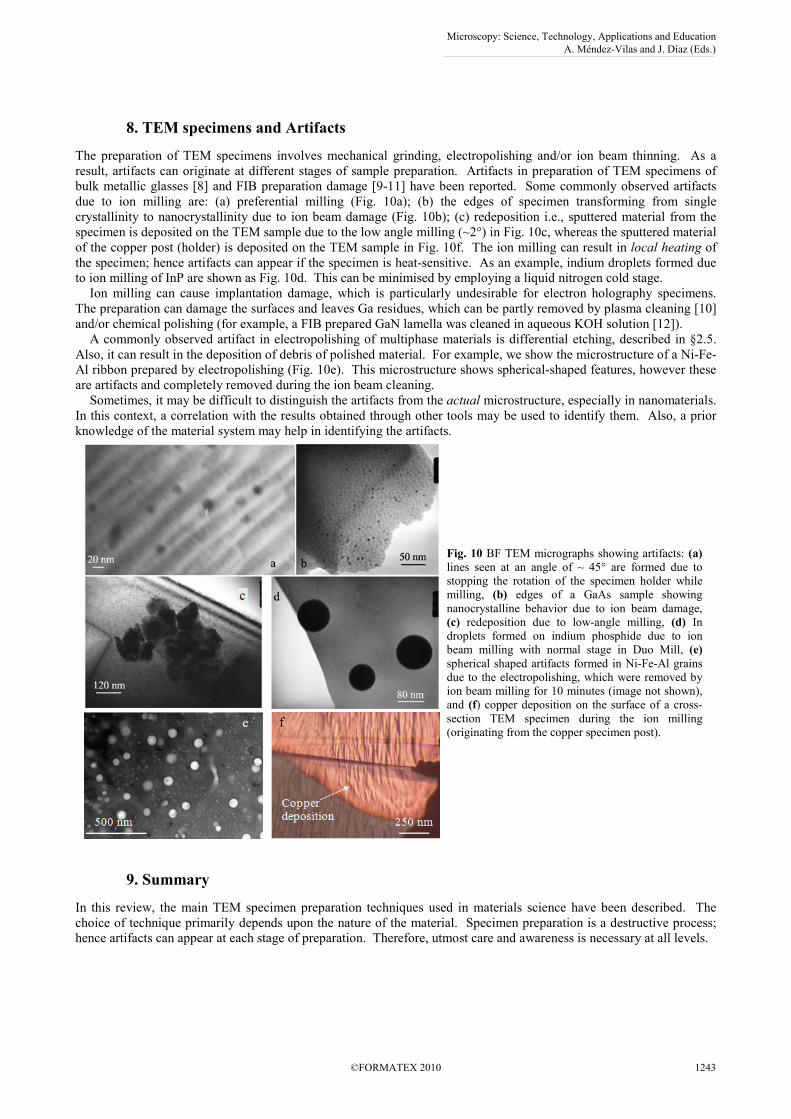
Fig. 10 BF TEM micrographs showing artifacts: (a)
lines seen at an angle of ~ 45° are formed due to
stopping the rotation of the specimen holder while
milling, (b) edges of a GaAs sample showing
nanocrystalline behavior due to ion beam damage,
(c) redeposition due to low-angle milling, (d) In
droplets formed on indium phosphide due to ion
beam milling with normal stage in Duo Mill, (e)
spherical shaped artifacts formed in Ni-Fe-Al grains
due to the electropolishing, which were removed by
ion beam milling for 10 minutes (image not shown),
and (f) copper deposition on the surface of a cross-
section TEM specimen during the ion milling
(originating from the copper specimen post).
Microscopy: Science, Technology, Applications and Education A. Méndez-Vilas and J. Díaz (Eds.)
©FORMATEX 2010 1243
______________________________________________
Acknowledgements This article is prepared from our technical report (DMRL 2006 419, 2006) published by DMRL, Hyderabad,
as well as from the original research conducted by DVSR in the University of Cambridge. DVSR thanks Prof. D. Banerjee (IISc,
Bangalore) for his kind support to start career in electron microscopy; Dr. R. Beanland (University of Warwick, UK), Mr. Zhen-Yu
Liu, Dr. M. Haeberlen and Dr. M. J. Kappers (University of Cambridge, UK) for useful interactions/images; and research
collaborators for the specimens. Special thanks to Dr. Rafal E. Dunin-Borkowski (Technical University of Denmark, Denmark) for
his kind suggestions. The authors thank DMRL and EPSRC (UK) for funding/permission to communicate this article.
References
[1] Thomson-Russel and Edington JW. Practical Electron Microscopy in Materials Science, Monograph 5, Macmillan, Philips
Technical Library, 1977.
[2] Goodhew PJ. Specimen preparation in Materials Science, North Holland Publishing Company, New York, 1973: 58
[3] Sridhara Rao DV, Balamuralikrishnan R, Muraleedharan K. Bulletin of Materials Science, 2004; 27(5) : 471-482
[4] Scott McCaffrey, The Small Angle Cleavage Technique: An Update, Materials Research Society, Vol. 480 (1997). [5] Beanland R, Microscopy Today, 2003; 11(1) : 29-31
[6] http://www.mse.eng.ohio-state.edu/~COLIJN/tripod_course.pdf
[7] http://www.imec.be/efug/EFUG10.html
[8] Sun BB, Wang YB, Wen J, Hang H, Sui ML, Wang JQ, and Ma E. Scripta. Mat. 2005; 53(7) : 805-809
[9] Joachim Mayer, Lucille A. Giannuzzi, Takeo Kamino, and Joseph Michael, MRS Bulletin, 2007; 32 : 400-407
[10] Dong-Su Ko, Young Min Park, Sung-Dae Kim, and Young-Woon Kim, Ultramicroscopy, 2007; 107(4-5) : 368-373
[11] David Cooper, Robert Truche, Jean-Luc Rouviere, Ultramicroscopy, 2008(5); 108: 488-493
[12] Jinschek JR, Radmilovic V, Kisielowski Ch, Microsc. Microanal. 10(Suppl.2), 2004; 1142-1143
Microscopy: Science, Technology, Applications and Education A. Méndez-Vilas and J. Díaz (Eds.)
1244 ©FORMATEX 2010
______________________________________________