Telluride Solar C Fabricated by Electrodeposition · of deposition time provides a simple way to...
46
April 1997 • EL/SR-520-21927 � . Film Cadmium Polycrystalline Telluride Solar C Electrodeposition Annual Technical 20 March 1995- 19 Fabricated by o h 1996 J.U.Trey and D. Mao Colorado School of Mines Golden, Colorado National Renewable Energy Laboratory 1617 Cole Boulevard Golden, Colorado 80401-3393 A national laboratory of the U.S. Department of Energy Managed by Midwest Research Institute for the U.S. Department of Energy under Contract No. DE-AC36-83CH10093
Transcript of Telluride Solar C Fabricated by Electrodeposition · of deposition time provides a simple way to...

April 1997 • NREL/SR-520-21927
� ..... Film Cadmium Polycrystalline Telluride Solar C Electrodeposition
Annual Technical 20 March 1995- 19
Fabricated by
ort h 1996
J.U.Trefny and D. Mao Colorado School of Mines Golden, Colorado
National Renewable Energy Laboratory 1617 Cole Boulevard Golden, Colorado 80401-3393 A national laboratory of the U.S. Department of Energy Managed by Midwest Research Institute for the U.S. Department of Energy under Contract No. DE-AC36-83CH10093

,, (
NREL/SR-520-21927 • UC Category: 1263 • DE96014325
Poly crystalline Telluride Solar Electrodeposition
Annual Technical 20 March 1995-
Film Cadmium Fabricated by
J.U.Trefny and D. Mao Colorado School of Mines Golden, Colorado
NREL technical monitor: B. von Roedem
�·� .r-1.�1,=• ..... --•
National Renewable Energy Laboratory 1617 Cole Boulevard Golden, Colorado 80401-3393 A national laboratory of the U.S. Department of Energy Managed by Midwest Research Institute for the U.S. Department of Energy under Contract No. DE-AC36-83CH10093
Prepared under Subcontract No. XAF-5-14142-11
April 1997
This publication was reproduced from the best available camera-ready copy submitted by the subcontractor and received no editorial review at NREL.
NOTICE
This report was prepared as an account of work sponsored by an agency of the United States government. Neither the United States government nor any agency thereof, nor any of their employees, makes any warranty, express or implied, or assumes any legal liability or responsibility for the accuracy, completeness, or usefulness of any information, apparatus, product, or process disclosed, or represents that its use would not infringe privately owned rights. Reference herein to any specific commercial product, process, or service by trade name, trademark, manufacturer, or otherwise does not necessarily constitute or imply its endorsement, recommendation, or favoring by the United States government or any agency thereof. The views and opinions of authors expressed herein do not necessarily state or reflect those of the United States government or any agency thereof.
#.
Available to DOE and DOE contractors from: Office of Scientific and Technical Information (OSTI) P.O. Box62
Oak Ridge, TN 37831 Prices available by calling (423 ) 576-8401
Available to the public from: National Technical Information Service (NTIS) U.S. D epartment of Commerce 5285 Port Royal Road Springfield, VA 22161 (703) 487-4650
f.J' Printed on paper containing at least 50% wastepaper, including 20% postconsumer waste
NOTICE
This report was prepared as an account of work sponsored by the National Renewable Energy Laboratory, managed by Midwest Research Institute, in support of its Subcontract No. XAF-5-14142-1 1 with Colorado School of Mines. Neither the National Renewable Energy Laboratory, nor the Midwest Research Institute, nor Colorado School of Mines, nor any of their employees, nor any of their contractors, nor any of their subcontractors, nor any of their employees, makes any warranty, express or implied, or assumes any legal liability or responsibility for the accuracy, completeness or usefulness of any information, apparatus, product or process disclosed, or represents that its use would not infringe privately owned rights
11

·,
Executive Summary
Objectives
The objective of this project is to develop improved processes for the fabrication of CdTe/CdS polycrystalline thin fllm solar cells. The technique we use. for the formation of CdTe, electrodeposition, is a non-vacuum, low-cost technique that is attractive for economic, large-scale production.
Technical Approach
During the past year, our research and development efforts have focused on several steps that are most critical to the fabrication of high-efficiency CdTe solar cells. These include the optimization of CdTe electrodeposition process, the effect of pre-treatment of CdS substrates, the post-depositionannealing of CdTe, and back contact formation using Cu-doped ZnTe. Systematic investigations of these processing steps have lead to better understanding and improved device performances of the CdTe-based solar cells.
Results
Studies of the �rowth and properties ofCBD CdS tbjo films. The structural properties of the fllmsand the growth mechanisms were studied by investigating CdS samples prepared at different deposition times. A duplex structure with an inner compact layer and an outer porous layer and three growth stages is consistent with our data. The measurement of refractive index as a function of deposition time provides a simple way to determine the transition point from compact layer growth to porous layer growth, which is important for the optimization of CdS growth conditions in photovoltaic applications. Careful XRD analyses allowed unambiguous determination of crystal properties.
EffectofCdCl, treatmentofCdS films. We-investigated the effect of CdCl2 treatment of CdS filmson the photovoltaic performance of CdTe solar cells. X -ray diffraction studies indicated that the diffusion of S into CdTe is qualitatively the same for CdTe/CdS films fabricated with both asdeposited and CdCl2-treated CdS. A major difference was observed in the extent of Te diffusion into CdS for the two types of CdS films. Full conversion of CdS into CdS 1.yTey was observed for films prepared with as-deposited CdS, while the formation of the ternary phase was below the detection limit for films prepared with CdCl2-treated CdS. Photoluminescence measurements confirmed this result. The difference in interdiffusion leads to differences in optical transmission of CdS films and spectral response of CdTe/CdS solar cells. An increase of 2.7 mA/cm2 in short-circuit currentdensity was observed as a result of improved spectral response in the wavelength range of 500-600 nm for the CdCl2-treated CdS.
Studies of Cu-doped ZnTe back contact layer. Cu-doped ZnTe was studied as a promising materialfor forming stable, low-resistance contacts to the p-type CdTe. Polycrystalline ZnTe fllms were formed by vacuum co-evaporation of Cu and ZnTe. The electrical properties were studied systematically as a function of Cu concentration and annealing temperature. The effects of Cu
concentration, ZnTe post-deposition annealing temperature, and the types of metals used to contact ZnTe on solar cell performances were studied. A Cu concentration of 5.4 at. %, a ZnTe postdeposition annealing temperature of 170oC, and Au metal contact on ZnTe were found to yield the highest cell performances. Different metal contacts on the ZnTe layer lead to different CdTe doping densities, which in tum may contribute to differences in the diffusion potential at the CdTe/CdSjunction and the open-circuit photo voltage of the solar cells. The formation of a back contact diode at the CdTe/ZnTe interface was detected for Ni-contacted cells, based on capacitance-voltage analysis. The series resistance of the CdTe/CdS cells was reduced significantly by the introduction of the ZnTe layer. Fill factors greater than 0.70 were consistently obtained, with the highest value reaching 0.76.
Optimization of CdTe and CdS film thicknesses. We have investigated the effect of CdTe and CdSthickness on the photovoltaic performance of the resulting cells. We found that an increase in the CdTe thickness from 2 J.lm to 3. 5 J.lm lead to a consistent improvement in V oc by 40-60 m V. Theshunt resistance of the cells was also increased. As a result, V oc greater than 800 m V and Rsh greaterthan 1000 n cm2 were regularly obtained. SEM measurements indicated that the average CdTegrain size after CdCb treatment and annealing was much larger for the thicker CdTe films. CdS layer thickness was varied from 700 A. to over 4000 A., The most efficient cells were obtained with1500 A. CdS. For cells made with thinner CdS, both V oc and shunt resistance deteriorated becauseof the significant consumption of CdS during CdS-CdTe interdiffusion.
As a result of our systematic investigation and optimization of the processing conditions, we have improved the efficiency of CdTe/CdS cells using ZnTe back contact and electrodeposited CdTe. Our best CdTe/CdS cell exhibited a V oc of 0.778 V, a J.., of 22. 4 mA/cm2, an FF of74. 0%, and anefficiency of 12.9% (verified at NREL). In terms of individual parameters, we have obtained V oc
over 0. 8 V and FF of76% on other cells.
iv

1.
2.
3.
Executive Summary
Table of Contents
List of Figures
List of Tables
Introduction
1.1 Background
Table of Contents
1.2 Cell Fabrication Procedure
Growth and Properties of Chemical Bath Deposited CdS Thin Films
2.1 CdS Growth Process
2.2 Structural Properties of CdS Films
2.2 Electrical Properties of CdS Films
CdTe-CdS Interdiffusion Studies
3.1 Interdiffusion During Post-deposition Annealing of CdTe
3.2 Effect of CdClz Treatment of CdS
iii
v
VI
Vlll
1
1
1
2
2
5
8
10
10
14
4. Study of ZnTe:Cu Back Contacts on CdTe/CdS Thin Film Solar Cells 21
4.1 Optimization of the ZnTe:Cu Layer and Its Processing Conditions 21
4.2 Mechanism and Stability Studies 23
5. Solar Cell Performances and Analysis 28
6.
7.
8.
9.
Summary
Acknowledgements
References
Appendices
9.1 Personnel
9.2 Publications
32
33
33
35
35
36

List of Figures
Figure 2.1 CdS film thickness as a function of deposition time.
Figure 2.2. Refractive index of CdS as a function of deposition time.
Figure 2.3. CdS grain size as a function of film thickness.
Figure 2.4. CdS surface roughness as a function of CdS film thickness.
Figure 2.5. XRD patterns of CdS films: (a) A film obtained in the compact layer growth stage; (b)A film obtained in the porous layer growth stage.
Figure 2.6. XRD patterns of CdS powders: (a) Powders extracted from the solution; (b) Powdersscrapped from the substrates.
Figure 3.1. XRD patterns of the (531) peak from different CdTe samples: annealed film, as-deposited film, and CdTe powders.
Figure 3.2. Lattice constants ofCdTe. (a) commercial CdTe powder (99.999%); (b) CdTe thin film annealed at 410°C for 50 min; (c) CdTe powder collected from scraping off the CdTe thin film corresponding to (b) from glass substrate.
Figure 3.3. Comparison of the XRD lineshape of the thin film and the powder collected from scraping off the thin film from glass substrate.
Figure 3.4. Effect of CdC12 treatment on CdTe/CdS interdiffusion. (a) CdTe annealed at 350°C, showing no interdiffusion; (b) CdTe annealed at 410oC without CdCl2, showing limitedinterdiffusion; (c) CdTe annealed at 410oC with CdCb, showing significant interdiffusion.
Figure 3.5. Spectral response of CdTe/CdS solar cells prepared with as-deposited (dashed) and CdCl2-treated CdS (solid).
Figure 3.6. XRD patterns of the CdTe (531) peak from CdTe/CdS films prepared with (a) asdeposited and (b) CdCb-treated CdS.
Figure 3.7. XRD patterns of the CdS (103) peak from CdTe/CdS films prepared with as-deposited (open circles) and CdCl2-treated CdS (solid circles).
Figure 3 .8. (a) Corrected optical transmission of CdS films prior to CdTe deposition. (b) Opticalabsorption of CdS as a function of photon energy. dashed: as-deposited CdS; solid: CdClrtreated CdS.
Figure 3.9. (a) Corrected optical transmission of CdS films after CdTe/CdS interdiffusion. (b)
Vl
. (ahv)2 vs. hv plot ofCdS after CdTe/CdS interdiffusion. dashed: as-deposited CdS; solid: CdChtreated CdS.
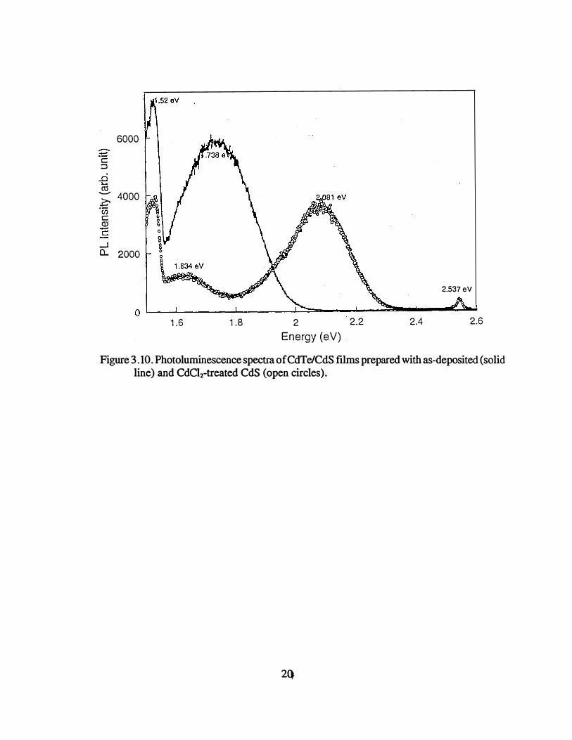
Figure 3.10. Photoluminescence spectra ofCdTe/CdS films prepared with as-deposited (solid line) and CdCl2-treated CdS (open circles).
Figure 4.1. 1/C2 vs V plots of CdS/CdTe/ZnTe cells using Au and Ni as contact metals to ZnTe.
Figure 4.2. 1/C2 vs. V plots of CdS/CdTe!ZnTe cells with different ZnTe:Cu layer thickness. (a) Au as contact metal to ZnTe; (b) Ni as contact metal to ZnTe. ZnTe layer thickness: 400 A (O ), 900A (.t..), and 1500 A (c).
Figure 5.1. SEM images of CdTe films after CdCb-treatment and 4HPC-annealing. The CdTe film thickness was (a) 2.2 Jlm and (b) 3.4 Jlm.
Figure 5.2. Light I-V curve (measured at NREL) of a CdS/CdTe/ZnTe/Au cell showing 12.9% efficiency.
Figure 5.3. Spectral response curve (measured at NREL) of a CdS/CdTe!ZnTe/Au cell with 12.9% efficiency.
vii

List of Tables
Table 2.1. Lattice spacing and relative integrated intensity of standard hexagonal and cubic CdS powders and CdS powers removed from the glass substrates and extracted from the chemical solutions.
Table 2.2. Recipes for chemical bath deposition of CdS.
Table 2.3. Electrical Properties of CdS films prepared by fast growth.
Table 2.4. Electrical Properties of CdS films prepared by slow growth.
Table 3.1. Dependence of photovoltaic performance on the amount of CdCh used for annealing.
Table 3.2. Photovoltaic performance of CdS/CdTe cells fabricated with as-deposited and CdC12-treated CdS films.
Table 4.1. Effect of Cu concentration in ZnTe on Au/ZnTe/CdTe/CdS cell performances.
Table 4.2. Effect of ZnTe annealing temperature and back contact metal on cell performances. The Cu concentration in ZnTe was 5.5 at. %.
Table 4.3. Diode quality factors (A), saturation current density (J 0), and series resistance (Rs) of CdTe/CdS cells with and without a ZnTe layer.
Table 4.4. V oc and its stability of CdS/CdTe/ZnTe cells and the doping concentration deduced from dark C-V curves.
Table 5 .1. Effect of CdS thickness on the photovoltaic performance of CdTe/CdS cells.
Table 5.2. Effect of CdTe thickness on cell performances.
viii
1. Introduction
1.1 Background
Polycrystalline thin-film CdTe has attracted a great deal of interest for low-cost, highefficiency photovoltaic energy conversion applications. Among the various techniques that are available for CdTe thin
.film deposition, electrodeposition is a non-vacuum technique and has the
advantage of low cost, efficient utilization of raw material, and scalability for high-volume production. At the same time, additional research is still needed to improve upon the efficiencies and performance levels achieved to date. Among the significant issues are interface carrier recombination and top-layer photon absorption which presently limit the short-circuit current, junction recombination which limits the open-circuit voltage, and series-resistance losses which suppress the fill-factor.
The objective of the CSM contract was to improve certain processing steps of the cell fabrication and to further our knowledge of these polycrystalline thin film materials. Improved efficiencies, high-quality film growth techniques, materials analysis, device fabrication and characterization have all been of particular interest in our work.
1.2 Cell Fabrication Procedure
The solar cell structure we investigate has a CdTe/CdS/SnO/glass structure. The standard cell fabrication procedure includes:
(1) Chemical bath deposition (CBD) of CdS layers. (typical thickness of 0.2 J.Lm) in an
alkaline solution containing cadmium acetate, ammonium acetate, ammonium hydroxide, and thiourea (see Section 2.3 for the solution composition).
(2) Annealing of the CdS films at 450°C for 50 min in a N2 atmosphere. A CdCh coating was applied to the CdS surface prior to annealing, using a mist generator containing a 1.2 M CdCl2 aqueous solution.
(3) The electrodeposition of CdTe (typical thickness of 2 - 3.5 J.Lm) using a system composed of four electrodes: Cd and Te anodes, a Ag/ AgCl reference electrode, and a cathode (sample substrate). The typical electroplating conditions were: pH, 2; temperature, 80°C; 1.2 M CdCl2 ; deposition current between 0.26 and 0.40 mA/cm2; deposition potential, -600 mV (vs.Ag/AgCl electrode); and anode current ratio close to 2.0.
( 4) Annealing of CdTe/CdS films at 410oC for 40 min in dry air. Prior to annealing, a CdChcoating was applied to the CdTe surfaces using the same procedure as used for the CdS layers.
(5) Etching of the CdTe surface in a 0.1% Br-MeOH solution for 10 s and back contact formation using either evaporated Au or Cu-doped ZnTe followed by Au evaporation.
A wide variety of thin film and device characterization techniques were used to characterize our material. X-ray diffraction (XRD) measurements were performed on a Rigaku x-ray diffractometer using Cu-Ka radiation. Scanning electron microscopy (SEM) measurements were performed using a JOEL Model840 instrument. Optical transmission and reflection measurements were performed using a CARY 5E UV-VIS-NIR spectrophotometer equipped with a PTFE
l
integrating sphere. Film thicknesses were measured using a Dektak 3 surface profiler. For the study of structural and optical properties of the CdS films after CdTe deposition and final annealing processes, the CdTe layers were removed either mechanically or by chemical etching. The finished cells were characterized using current-voltage, capacitance-voltage, and spectral response techniques.
2. Growth and Properties of Chemical Bath Deposited CdS Thin Films
CdS is commonly used as n-type window layers in CdTe solar cells. Among various techniques for preparing CdS fllms, chemical bath deposition (CBD) is a simple and low-cost method and produces uniform, adherent, and reproducible films. There have been several studies [1-4] on the mechanism of CdS growth via CBD as it relates to the optimization of CdS film properties. It is well known that, depending on the deposition conditions, an "ion-by-ion" growth process results in compact and adherent films while a "cluster-by-cluster" process or colloidal growth yields porous films [1,5]. Recently, Lincot and Borges [2,3] have carried out detailed insitu studies on the CdS CBD process, using quartz crystal microbalance and electrochemical impedance measurement techniques. A more detailed duplex layer structure of CdS fllms and three distinct stages of CdS fllm growth were proposed [2,3].
We studied CdS films of various thicknesses corresponding to the termination of the growth at different deposition stages. CdS thin film samples were prepared on glass slides by CBD from an ammonia-thiourea aqueous solution. The chemicals and their concentrations in the solution were: CdAc2 (1x10⁻³ M), NH�c (20x1D-3 M), and (NH2)2CS (5x1Q-3 M). Ammonia was used to adjust the initial solution pH to a value between 9 and 10. The chemical bath was kept at a temperature of 85<C. The substrates were immersed in the solution and taken out at different deposition times. The mechanism of CdS growth, the structural properties of these films and the compactness of the fllms were then analyzed using XRD, ellipsometry and other measurements.
2.1 CdS Growth Process
It is known that chemical bath deposition of CdS proceeds in three main stages [2]: an induction stage, a compact layer growth stage and a porous layer growth stage. The induction region corresponds to the formation of nucleation sites on the substrate. Following this induction period is the growth of a compact layer that is usually completed at a thickness between 100 and 200 nm [ 1 ,3]. Afterwards, a porous layer is formed for longer deposition time. Finally, the solution species are exhausted and the CdS film growth ceases. If CdS film growth proceeds into the porous layer growth region, a duplex layer structure, which consists of an inner compact layer and an outer porous layer with some surface particles, will be formed.
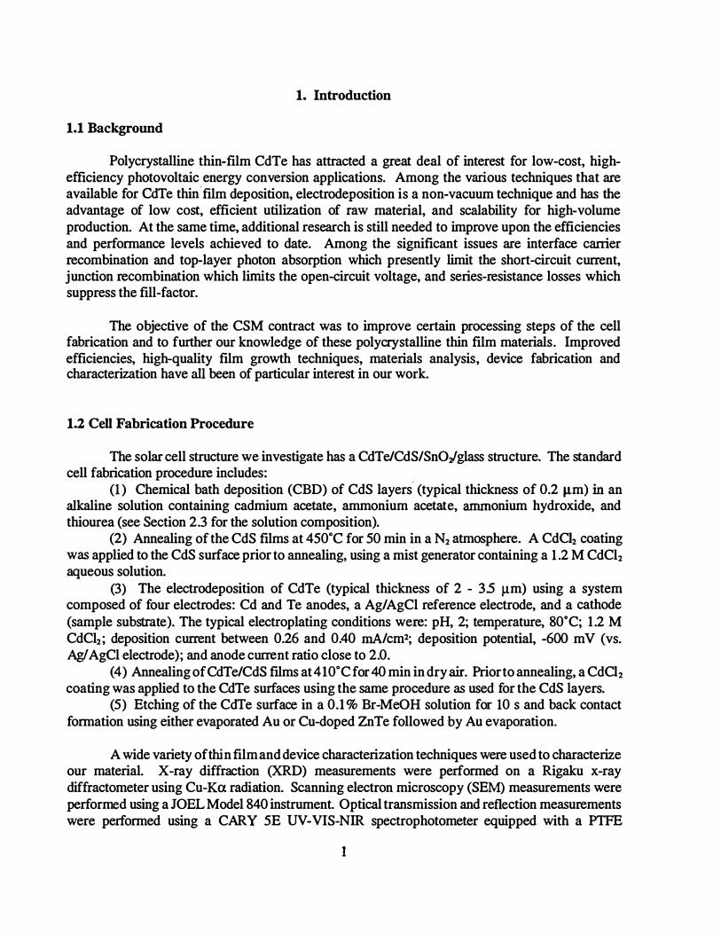
Figure 2.1 shows the CdS film thickness as a function of deposition time. The induction period is clear (about 15 min); after that, CdS thickness is measurable and increases approximately linearly with deposition time. The growth rate decreases after 40 min because of a depleting solution. From the growth curve, we cannot determine the point of transition from compact to porous layer growth. Reportedly [2,3], there is a small plateau on the growth curve which indicates
2
this transition point; after the plateau, a sudden increase of the growth rate generally takes place, corresponding to the start of a porous layer growth. However, evidence of such behavior is not obvious if the thickness measurement is not precise enough.
-
E c
- 200en en Q)c�()
..s:::: 100I-E iL.
0 0 20 40 60
Deposition Time ( Minutes )
Figure 2.1 CdS film thickness as a function of deposition time.
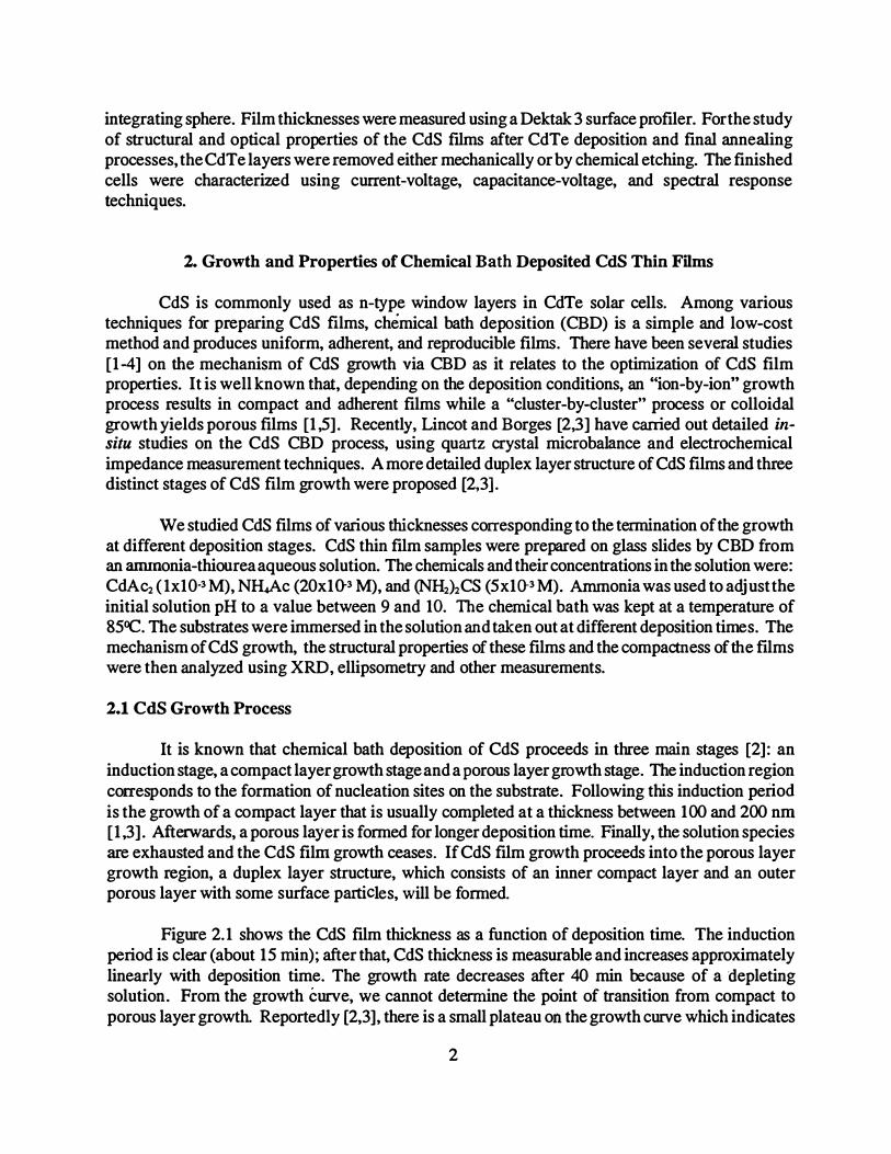
Studies of the evolution of the refractive index provide a simple quantitative method to determine the transition point from compact layer growth to porous layer growth. Figure 2.2 shows the refractive index, obtained from optical reflection and transmission measurements, as a function of deposition time. In the compact layer growth region, CdS does not fully cover the substrate. Thiscontributes to an artificially smaller refractive index in comparison to that of bulk CdS. Near the transition point from the compact layer growth to the porous layer growth, the refractive index is close to that of bulk CdS (2.40) and reaches its maximum value (2.35). As porous layer growth starts, the refractive index decreases. Refractive index values measured from ellipsometry show qualitatively the same trend. In order to obtain dense CdS films, the substrates need to be removed from the bath just prior to porous layer growth (35 min here).
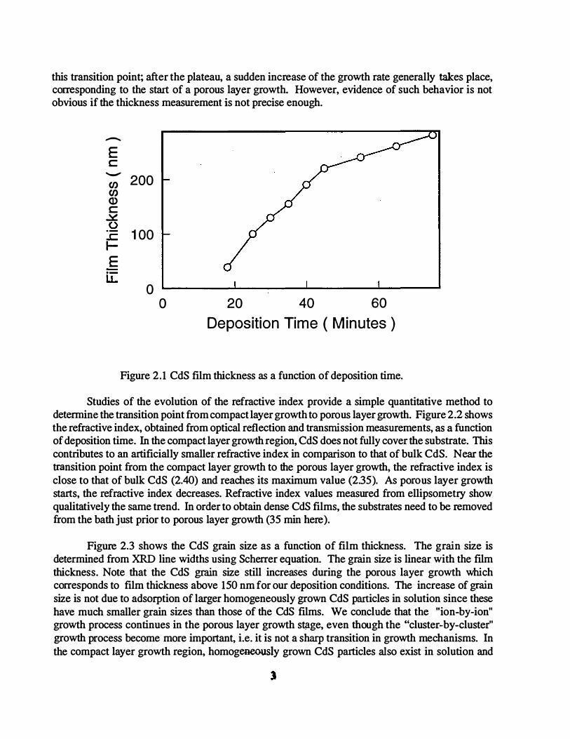
Figure 2.3 shows the CdS grain size as a function of film thickness. The grain size is determined from XRD line widths using Scherrer equation. The grain size is linear with the film thickness. Note that the CdS grain size still increases during the porous layer growth which corresponds to film thickness above 150 nm for our deposition conditions. The increase of grain size is not due to adsorption of larger homogeneously grown CdS particles in solution since these have much smaller grain sizes than those of the CdS films. We conclude that the "ion-by-ion" growth process continues in the porous layer growth stage, even though the "cluster-by-cluster" growth process become more important, i.e. it is not a sharp transition in growth mechanisms. In the compact layer growth region, homogeneously grown CdS particles also exist in solution and
are adsorbed on the substrates. However, in this region, film growth is dominated by the "ionby-ion" process.
>< Q)"0 2c: Q)>':.;j0� 1.5-Q) a:
20 40 60Deposition Time ( Minutes )
Figure 2.2. Refractive index of CdS as a function of deposition time.
- 80 E c 60-
(1)N ·- 40 (/) cctS 20 ,_
CJ 0
0 100 200 Film Thickness ( nm )
Figure 2.3. CdS grain size as a function of film thickness.
4

Figure 2.4 shows the CdS surface roughness as a function of CdS film thickness. This roughness is mainly due to height difference of CdS surface particles adsorbed from solution. In the compact layer growth region, the amount and size of adsorbed CdS surface particles are relatively small. In the porous layer growth region, on·the other hand, the roughness is relatively large and increases fast. This is consistent with our SEM and optical microscopy observations of CdS surfaces.
-
E c:
-
en en co 100 c
..c:C>::J0
a: 50 co0ca
't:::J (J) 0 0 100 200
Film Thickness ( nm )
2.2 Structural Properties of CdS Films
Figure 2.4. CdS surface roughness as a function of CdS film thickness .
There have been a lot of reports [5-9] on the structural properties of CdS films prepared by CBD. However, the results are scattered over a wid� range because of different deposition conditions used in various laboratories. X-ray diffraction (XRD) analysis is commonly used for structural studies. Because high quality as-deposited CdS films have only one preferred orientation, corresponding to either cubic (Il l) or hexagonal (002), it is difficult to distinguish these two phases based on the XRD peak position [5,6]. The study by Kaur et al[l] concluded that the " ion-byion" process results in compact films which have pure hexagonal or a mixture of hexagonal andcubic phase, and that the "cluster-by-cluster" process gives rise to porous layers with pure cubic phase . This point of view influenced other authors' assumptions on the phase of as-deposited CdS [4].
Figure 2.5 (a) and (b) show the XRD patterns for a CdS film obtained in the compact layergrowth stage and a film obtained in porous layer growth stage, respectively. Both films have a strong preferred orientation. The strong peak may correspond to cubic (Il l) with lattice spacing3.360 A or hexagonal (002) with a lattice spacing 3.367 A. It is difficult to distinguish the phase
s
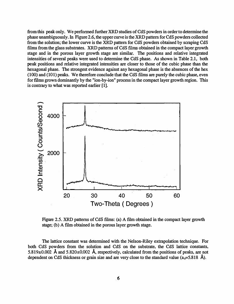
from this peak only. We performed further XRD studies of CdS powders in order to determine the phase unambiguously. In Figure 2.6, the upper curve is the XRD pattern for CdS powders collectedfrom the solution; the lower curve is the XRD pattern for CdS powders obtained by scraping CdS films from the glass substrates. XRD patterns of CdS films obtained in the compact layer growthstage and in the porous layer growth stage are similar. The positions and relative integrated intensities of several peaks were used to determine the CdS phase. As shown in Table 2.1, bothpeak positions and relative integrated intensities are closer to those of the cubic phase than the hexagonal phase. The strongest evidence against any hexagonal phase is the absences of the hex (100) and (101) peaks. We therefore conclude that the CdS films are purely the cubic phase, evenfor ftl.ms grown dominantly by the "ion-by-ion" process in the compact layer growth region. This is contrary to what was reported earlier [1].
-
'Uc00Q)
enen +J c::J0
0-
�.:t:::= encQ)+J c0a: ><
4000
2000
20 30 40 50 Two-Theta ( Degrees )
60
Figure 2.5. XRD patterns of CdS films: (a) A film obtained in the compact layer growthstage; (b) A fllm obtained in the porous layer growth stage.
The lattice constant was determined with the Nelson-Riley extrapolation technique. For both CdS powders from the solution and CdS on the substrate, the CdS lattice constants, 5.819±0.002 A and 5.820±0.002 A, respectively, calculated from the positions of peaks, are notdependent on CdS thickness or grain size and are very close to the standard value (ao=5.818 A) .
. 6
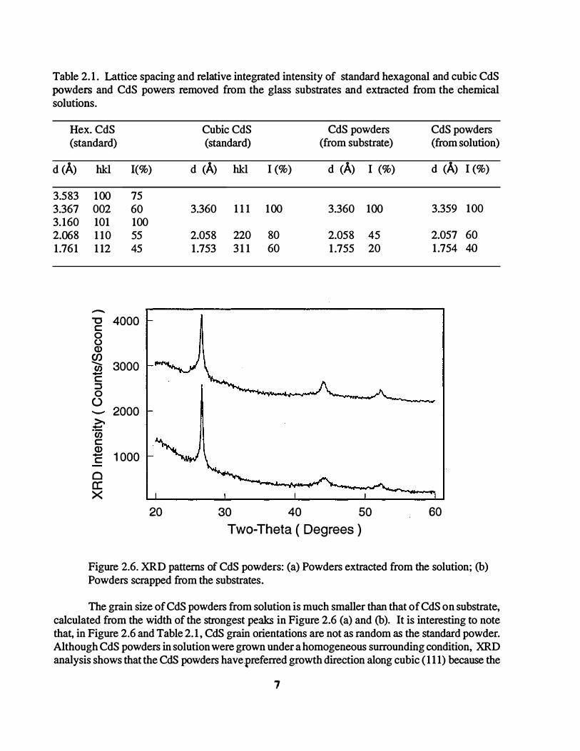
Table 2.1. Lattice spacing and relative integrated intensity of standard hexagonal and cubic CdS powders and CdS powers removed from the glass substrates and extracted from the chemical solutions.
Hex. CdS (standard)
d (A) hid I(%)
3.583 100 75 3.367 002 60 3.160 101 100 2.068 110 55 1.761 112 45
-""C 4000c: 0 0 Q) fQ 3000C/) -c: :J 0
(.) - 2000>.
:=: C/) c: Q) 1000-c:
Qa:X
20
Cubic CdS CdS powders (standard) (from substrate)
d <A>
3.360
2.058 1.753
hid I (%) d <A> I (%)
111 100 3.360 100
220 80 2.058 45 311 60 1.755 20
30 40 50Two-Theta ( Degrees )
CdS powders (from solution)
d (A) I (%)
3.359 100
2.057 60 1.754 40
60
Figure 2.6. XRD patterns of CdS powders: (a) Powders extracted from the solution; (b)Powders scrapped from the substrates.
The grain size of CdS powders from solution is much smaller than that of CdS on substrate, calculated from the width of the strongest peaks in Figure 2.6 (a) and (b). It is interesting to notethat, in Figure 2.6 and Table 2.1, CdS grain orientations are not as random as the standard powder. Although CdS powders in solution were grown under a homogeneous surrounding condition, XRD analysis shows that the CdS powders have.preferred growth direction along cubic ( 111) because the
7
grain size ratio in the (111), (220), and (311) orientations calculated from corresponding peaks is 3:1:1. This indicates that CdS grows more easily and faster along cubic (111) than along other directions. This is consistent with that fact that the CdS films on substrates have strong preferred orientation along cubic (111).
2.3 Electrical Properties of CBD CdS Films
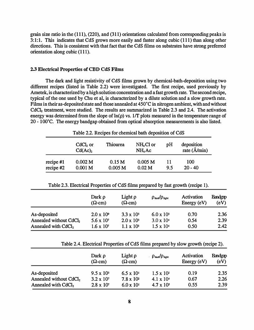
The dark and light resistivity of CdS films grown by chemical-bath-deposition using two different recipes (listed in Table 2.2) were investigated. The first recipe, used previously by Ametek, is characterized by a high solution concentration and a fast growth rate. The second recipe, typical of the one used by Chu et al, is characterized by a dilute solution and a slow growth rate. Films in their as-deposited state and those ·annealed at 450°C in nitrogen ambient, with and without CdCh treatment, were studied. The results are summarized in Table 2.3 and 2.4. The activation energy was determined from the slope of ln(p) vs. Iff plots measured in the temperature range of 20 - 1 00°C. The energy bandgap obtained from optical absorption measurements is also listed.
Table 2.2. Recipes for chemical bath deposition of CdS
recipe#l recipe#2
CdCl2 or Cd(Ac)z
0.002M 0.001 M
Thiourea
0.15M 0.005M
NJLCl or NJLAc
0.005 M 0.02M
pH
11 9.5
deposition rate (Almin)
100 20-40
Table 2.3. Electrical Properties of CdS films prepared by fast growth (recipe 1).
Darkp Light p p.wJplighl Activation (Q-cm) (Q-cm) Energy (eV)
As-deposited 2.0 X 10⁹ 3.3 X 10⁵ 6.0 X 10³ 0.70 Annealed without CdCl2 5.6 X 10⁷ 2.0 X 10³ 3.0 X 1(}4 0.54 Annealed with CdCb 1.6 X 10⁷ 1.1 X 10³ 1.5 X 1(}4 0.50
� (eV)
2.36 2.39 2.42
Table 2.4. Electrical Properties of CdS films prepared by slow growth (recipe 2).
Darkp Light p . p.wJplight Activation � (Q-cm) (Q-cm) Energy (eV) (eV)
As-deposited 9.5 X 10³ 6.5 X 101 1.5 X 10² 0.19 2.35 Annealed without CdCl2 3.2 X 10⁷ 7.8 X 10² 4.1 X 10⁴ 0.67 2.26 Annealed with CdCb 2.8 X 10⁷ 6.0 x 101 4.7 X 10⁵ 0.55 2.39
8
We can notice several features from these data:
(1) The bandgap of as-deposited CdS is comparable for films grown with either method and is 60 - 70 me V smaller than the bandgap of single crystal CdS. After CdCl2 treatment and annealing, the bandgap increases in both cases, approaching that of single crystal CdS (2.42 e V). For annealing without CdCl2, however, variations of bandgap in opposite directions were observed for films deposited with the 2 different recipes. A large decrease of bandgap was observed for films deposited with the slow growth recipe, whereas a small increase was observed for films deposited with the fast growth recipe.
(2) The dark resistivity of as-deposited films differs significantly, by more than 5 orders of magnitude, for film deposited with the 2 different recipes. The fast -growth recipe yielded very high dark resistivity and the slow-growth recipe yielded relatively low resistivity. Correspondingly, the activation energy is also much smaller in the latter case. After annealing, the dark resistivity reaches comparable values for both types of films�
(3) Films deposited by slow growth and annealed with CdC12 treatment showed the lowest resistivity under illumination (60 Q-cm) and the highest dark-to-light resistivity ratio (4.7 x 10⁵). The high conductivity under illumination and high dark-to-light resistivity ratio suggest a long lifetime of photogenerated electrons, an electron Fermi level close to the conduction ban.d, and, consequently, improved solar cell performances. Annealing of the slowly grown CdS with CdCl2 probably introduced a high concentration of hole traps which enhanced the photosensitivity.
(4) For both as-deposited films and those annealed without CdCh treatments, the photoconductivity decay is very slow. In some cases, several hours are required for the dark resistivity to reach a stable value. Such a slow decay of photoconductivity indicates the existence of high concentration of electron traps. For films annealed with CdCh treatment, the photoconductivity decay is very fast, with a time constant of the order of seconds. This indicates that the CdCl2 treatment eliminated effectively the electron trapping centers.
3. CdS-CdTe Interdiffusion Studies
3.1.Studies of CdTe Annealing and CdTe-CdS Interdiffusion
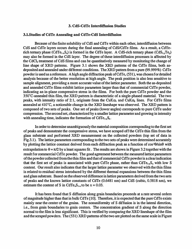
Because of the finite solubility of CdS and CdTe within each other, interdiffusion between CdS and CdTe layers occurs during the final annealing of CdS/CdTe films. As a result, a CdTerich ternary phase (CdTe1.xSJ is formed in the CdTe layer. A CdS-rich ternary phase (CdSt-y Tey) may also be formed in the CdS layer. The degree of these interdiffusion processes is affected by the CdCl2 treatment of CdS films and can be quantitatively measured by monitoring the change of line shape of XRD patterns. Figure 3.1 shows the XRD patterns of the CdTe films, both asdeposited and annealed under different conditions. The XRD pattern from a pure (99 .999%) CdTe powder is used as a reference. A high angle diffraction peak of CdTe, (531 ), was chosen for detailed analysis because of the better resolution at high angle. The peak position is also less sensitive to sample alignment, providing a more accurate value of the lattice parameter. Both the as-deposited and annealed CdTe films exhibit lattice parameters larger than that of commercial CdTe powder, indicating an in-plane compressive stress in the films. For both the pure CdTe powder and the 350°C-annealed thin film, the XRD pattern is characteristic of a single-phased material. The two peaks, with intensity ratio of 2: 1, originate from the CuKa.1 and CuKa.z lines. For CdTe films annealed at 410°C, a noticeable change in the XRD lineshape was observed. The XRD pattern is composed of two sets of peaks. One set of peaks (lower angles) corresponds to pure CdTe under compression. The second set, characterized by a smaller lattice parameter and growing in intensity with annealing time, indicates the formation of CdTe1.xSx.
In order to determine unambiguously the material composition corresponding to the first set of peaks and demonstrate the compressive stress, we have scraped off the CdTe thin film from the glass substrate and performed XRD measurement on the collected powders (top set of data in Fig.3.1 ). The lattice parameters corresponding to the two sets of peaks were determined accurately by plotting the lattice constant derived from each diffraction peak as a function of cos29/sin9 with extrapolation to e = 1t/2 by a least squares fit . The results are shown in Figure 3.2 together with the result for commercial CdTe powder. The good agreement between the measured lattice parameters of the powder collected from the thin film and that of commercial CdTe powder is a clear indication that the first set of peaks is associated with pure CdTe phase, rather than CdTet-xSx with low S content. Our result also indicates that the larger lattice parameter we observed with the thin films is related to residual stress introduced by the different thermal expansions between the thin films and glass substrate. Based on the observed difference in lattice parameters derived from the two sets of peaks and the known lattice constants of CdTe (0.6481 nm) and CdS (cubic, 0.5818 nm), we estimate the content of S in CdTexS1.x to be x = 0.03.
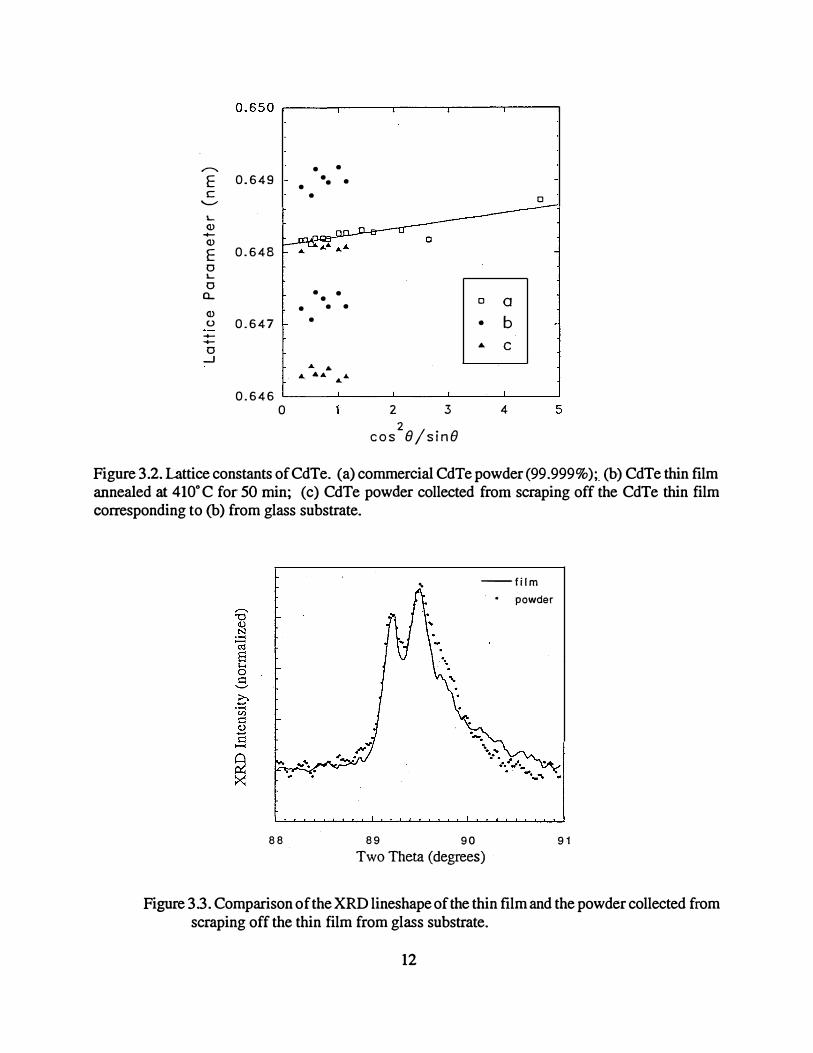
It has been found that S diffusion along grain boundaries proceeds at a rate several orders of magnitude higher than that in bulk CdTe [1 0]. Therefore, it is expected that the pure CdTe exists mainly near the center of the grains. The non uniformity of S diffusion is in the lateral direction, i.e., from grain boundaries to grain centers. The concentration gradient of S along the directionnormal to the film is less significant. This is verified by comparing the XRD lineshape of the film and the scraped powders. The ( 531) XRD patterns of the two are plotted on the same scale in Figure
10
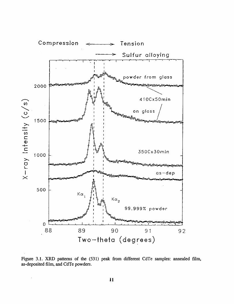
Figure 3.1. XRD patterns of the (531) peak from different CdTe samples: annealed film.as-deposited film, and CdTe powders.
0.650 .-----.-----.-----.-----.-----•
,.-..... • •
E 0.649 • • • • c • 0 ...___..
L (!)
..... (!)
E 0.648 0 L 0
Q.. • • • 0 a • • • (!) • b0 0.647 •
..... ..... ... c 0 _J ... ...
... ...... .......
0.646 0 2 3 4 5
2 cos e 1 sine Figure 3.2. Lattice constants of CdTe. (a) commercial CdTe powder (99 .999% );_ (b) CdTe thin filmannealed at 410° C for 50 min; (c) CdTe powder collected from scraping off the CdTe thin film corresponding to (b) from glass substrate.
88
.. -- film
89 90 Two Theta (degrees)
• powder
91
Figure 3.3. Comparison of the XRD lineshape of the thin film and the powder collected from scraping off the thin film from glass substrate.
12
l
I l
3.3. The pattern from the powder has been shifted to align with that of the film. It is clear that the Iineshapes .of the tWo are similar, especially in the vicinity of the sharp peak characteristic of the interdiffusion. This suggests that the S diffusion into the CdTe film and the distribution of CdTe 1_ xSx is nearly uniform in the direction perpendicular to the film. Otherwise, if S diffusion is limited to a region near the CdS/CdTe metallurgical junction which is buried under a pure CdTe layer, we would expect a much lower intensity of the second set of diffraction peaks from the thin film than from the collected powder because of the strong absorption of x-rays in the CdTe film. For CuKa radiation we used, the absorption coefficient of CdTe is 1408 em-•. At a diffraction angle of 29 =
89°, a 1J.Lm-thick CdTe layer would attenuate the XRD signal by more than 30%.
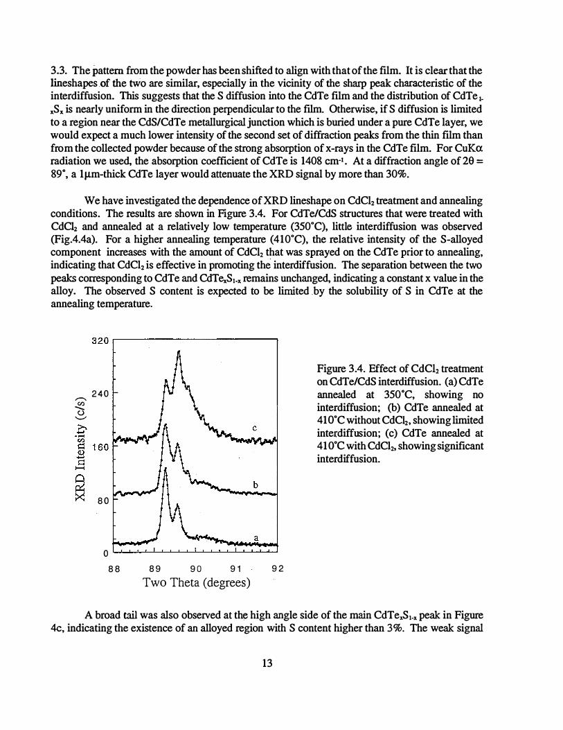
We have investigated the dependence ofXRD lineshape on CdCl2 treatment and annealing conditions. The results are shown in Figure 3A. For CdTe/CdS structures that were treated with CdCh and annealed at a relatively low temperature (350°C), little interdiffusion was observed (FigAAa). For a higher annealing temperature (410°C), the relative intensity of the S-alloyed component increases with the amount of CdClz that was sprayed on the CdTe prior to annealing, indicating that CdCl2 is effective in promoting the interdiffusion. The separation between the two peaks corresponding to CdTe and CdTexSt-x remains unchanged, indicating a constant x value in the alloy. The observed S content is expected to be limited .by the solubility of S in CdTe at the annealing temperature.
;--._ Cl)
0'--"
320 �--------------------------------------------�
240
b 80
0 L-.J.......L...-t-'-.L......J..-'-'--'--'--'---'-'--'--...l-1-'-.L.......L.-'
88 89 90 91 Two Theta (degrees)
92
Figure 3A. Effect of CdCh treatment on CdTe/CdS interdiffusion. (a) CdTe annealed at 350°C, showing no interdiffusion; (b) CdTe annealed at 41 OOC without CdC12, showing limited interdiffusion; (c) CdTe annealed at 41 ooc with CdCb, showing significant interdiffusion.
A broad tail was also observed at th� high angle side of the main CdTexS t-x peak in Figure 4c, indicating the existence of an alloyed region with S content higher than 3%. The weak signal
13
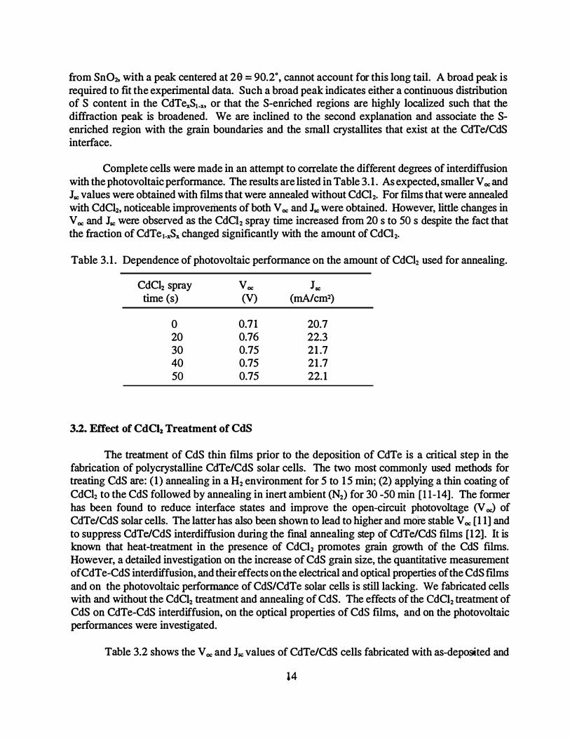
from Sn02, with a peak centered at 29 = 90.2°, cannot account for this long tail. A broad peak is required to fit the experimental data. Such a broad peak indicates either a continuous distribution of S content in the CdTexS1.x, or that the S-enriched regions are highly localized such that the diffraction peak is broadened. We are inclined to the second explanation and associate the Senriched region with the grain boundaries and the small crystallites that exist at the CdTe/CdS interface.
Complete cells were made in an attempt to correlate the different degrees of interdiffusion with the photovoltaic performance. The results are listed in Table 3.1. As expected, smaller V oc and Isc values were obtained with films that were annealed without CdCl2. For films that were annealedwith CdCh, noticeable improvements of both V oc and Isc were obtained. However, little changes inV oc and Isc were observed as the CdC12 spray time increased from 20 s to 50 s despite the fact thatthe fraction of CdTe,_xSx changed significantly with the amount of CdCb.
Table 3.1. Dependence of photovoltaic performance on the amount of CdCh used for annealing.
CdCl2 spray Voc Jsctime (s) (V) (mA/cm2)
0 0.71 20.7 20 0.76 22.3 30 0.75 21.7 40 0.75 21.7 50 0.75 22.1
3.2. Effect of CdCI2 Treatment of CdS
The treatment of CdS thin films prior to the deposition of CdTe is a critical step in the fabrication of polycrystalline CdTe/CdS solar cells. The two most commonly used methods for treating CdS are: (1) annealing in a H2 environment for 5 to 15 min; (2) applying a thin coating of CdCh to the CdS followed by annealing in inert ambient (N2) for 30-50 min [11-14]. The former has been found to reduce interface states and improve the open-circuit photovoltage (V oc) of CdTe/CdS solar cells. The latter has also been shown to lead to higher and more stable V oc [11] and to suppress CdTe/CdS interdiffusion during the final annealing step of CdTe/CdS films [12]. It is known that heat-treatment in the presence of CdCb promotes grain growth of the CdS films. However, a detailed investigation on the increase of CdS grain size, the quantitative measurement ofCdTe-CdS interdiffusion, and their effects on the electrical and optical properties of the CdS films and on the photovoltaic performance of CdS/CdTe solar cells is still lacking. We fabricated cells with and without the CdC12 treatment and annealing of CdS. The effects of the CdC12 treatment of CdS on CdTe-CdS interdiffusion, on the optical properties of CdS films, and on the photovoltaic performances were investigated.
Table 3.2 shows the V oc and Isc values of CdTe/CdS cells fabricated with as-deposited and
14
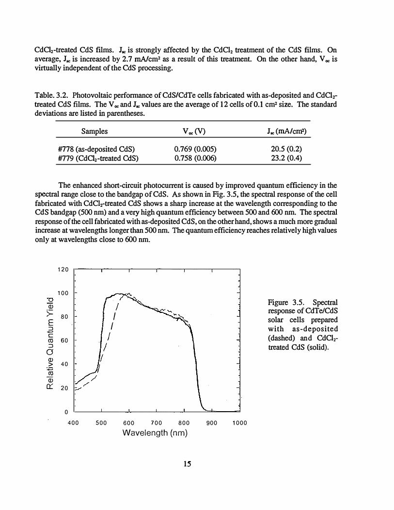
CdCh-treated CdS films. Isc is strongly affected by the CdCl2 treatment of the CdS films. On average, J.., is increased by 2.7 rnNcm2 as a result of this treatment. On the other hand, V oc isvirtually independent of the CdS processing.
Table. 3.2. Photo voltaic performance of CdS/CdTe cells fabricated with as-deposited and CdCbtreated CdS films. The V oc and Isc values are the average of 12 cells ofO.l cm2 size. The standarddeviations are listed in parentheses.
Samples
#778 (as-deposited CdS) #779 (CdCh-treated CdS)
v oc (V)
0.769 (0.005) 0.758 (0.006)
J.., (mA/cffil)
20.5 (0.2) 23.2 (0.4)
The enhanced short-circuit photocurrent is caused by improved quantum efficiency in the spectral range close to the bandgap of CdS. As shown in Fig. 3.5, the spectral response of the cell fabricated with CdClrtreated CdS shows a sharp increase at the wavelength corresponding to the CdS bandgap (500 nm) and a very high quantum efficiency between 500 and 600 nm. The spectral response of the cell fabricated with as-deposited CdS, on the other hand, shows a much more gradual increase at wavelengths longer than 500 nm. The quantum efficiency reaches relatively high values only at wavelengths close to 600 nm.
120
100 "0 Q)
>= 80 E:::l ........ c <U 60 :::l I aQ) I > 40 v :.;::::::; <U Q) /
0::: 20 / ;./
0
400 500
I I
I I
600 700 800
Wavelength (nm)
15
900 1000
Figure 3.5. Spectral response of CdTe/CdS solar cells prepared with as-d eposited (dashed) and CdCbtreated CdS (solid).
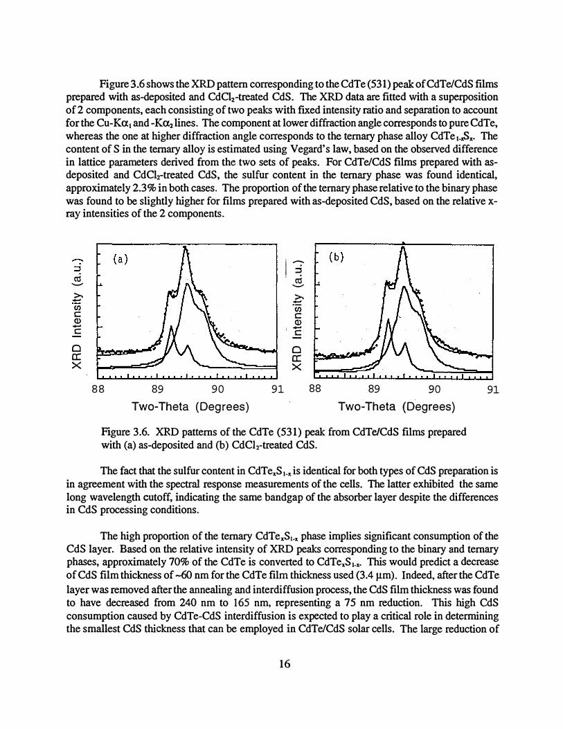
Figure 3.6 shows the XRD pattern corresponding to the CdTe (531) peak of CdTe/CdS films prepared with as-deposited and CdClz-treated CdS. The XRD data are fitted with a superposition of 2 components, each consisting of two peaks with fixed intensity ratio and separation to account for the Cu-Kat and-Ka2lines. The component at lower diffraction angle corresponds to pure CdTe, whereas the one at higher diffraction angle corresponds to the ternary phase alloy CdTet.xSx· The content of S in the ternary alloy is estimated using Vegard's law, based on the observed difference in lattice parameters derived from the two sets of peaks. For CdTe/CdS films prepared with asdeposited and CdClrtreated CdS, the sulfur content in the ternary phase was found identical, approximately 2.3% in both cases. The proportion of the ternary phase relative to the binary phase was found to be slightly higher for films prepared with as-deposited CdS, based on the relative xray intensities of the 2 components.
-:J ctl ..._..
>--en c (]) -c
0 a: X
88 89 90 91 Two-Theta (Degrees)
j;-. .ctl ..._..
>-::::: enc (]) ' -c
0 a: X
88 89 90 Two-Theta (Degrees)
Figure 3.6. XRD patterns of the CdTe (531) peak from CdTe/CdS films prepared with (a) as-deposited and (b) CdCI2-treated CdS.
91
The fact that the sulfur content in CdTexSt-x is identical for both types of CdS preparation is in agreement with the spectral response measurements of the cells. The latter exhibited the same long wavelength cutoff, indicating the same bandgap of the absorber layer despite the differences in CdS processing conditions.
The high proportion of the ternary CdTexSt-x phase implies significant consumption of the CdS layer. Based on the relative intensity of XRD peaks corresponding to the binary and ternary phases, approximately 70% of the CdTe is converted to CdTexSt-x- This would predict a decrease of CdS film thickness of -60 nm for the CdTe film thickness used (3.4 J.Lm)_ Indeed, after the CdTe
layer was removed after the annealing and interdiffusion process, the CdS film thickness was found to have decreased from 240 nm to 165 nm, representing a 7 5 nm reduction. This high CdS consumption caused by CdTe-CdS interdiffusion is expected to play a critical role in determining the smallest CdS thickness that can be employed in CdTe/CdS solar cells. The large reduction of
16

l [
l
CdS film thickness can also be · noticed when we compare CdTe/CdS cells fabricated withelectrodeposition and with closed-spaced sublimation (CSS). CSS is known to produce CdTe films with large grains and better crystallinity, which lead to less interdiffusion and less CdS consumption. On the other hand, electrodeposition and other low temperature processes produce CdTe films with much smaller grains, which lead to more significant interdiffusion and CdS consumption. This high CdS consumption caused by CdTe-CdS interdiffusion is expected to play a critical role in determining the smallest CdS thickness that can be employed in CdTe/CdS solar cells fabricated with low temperature processes. For example, if the smallest CdS thickness is -700 A for producingefficient cells using CSS deposited CdTe, a CdS thickness of 1200-1300 A would be the lower limitthat can be used for lower temperature processes such as electrodeposition.
2000 - Figure 3.7. XRD patterns �c of the CdS (103) peak
:::> from CdTe/CdS films .e 1 500<( prepared with as-deposited ........
(open circles) and CdCb-.c ·en 1 000 treated CdS (solid circles). c Q) c Cl a: 500 ·X
47.4 47.6 47.8 48 48.2 Two Theta (Degrees)
The diffusion of Te into CdS and the formation of CdS1.yTey were also investigated by monitoring the XRD pattern of the hexagonal CdS ( 1 03) peak (Fig. 3. 7). For this measurement, the bulk CdTe layer was removed chemically in a Br2-MeOH solution in order to enhance the XRD intensity of the CdS peak. In comparison to the CdTe XRD studies, a much more significant difference in the XRD patterns was observed in this case. For CdS/CdTe films prepared with CdCl2-treated CdS, the CdS (1 03) XRD peak yields a lattice spacing characteristic of pure CdS.For films prepared with as-deposited CdS, on the other hand, the XRD pattern shows a significant shift of the peak position toward low diffraction angle, indicating an increased lattice spacing and the formation of an alloyed phase. This indicates that while only a negligible portion of the CdS is converted to CdS,.y Tey for the CdC12-treated CdS, it is fully converted to the ternary phase when asdeposited CdS is used. Based on the known values of the (1 03) lattice spacing for CdS (0.1898 nm) and hexagonal CdTe (0.2115 nm), we estimate the y value to be 4.4% in CdS1.y Tey. This largedifference in the extent of Te diffusion into CdS is expected to originate from not only the differences in grain size, but also the differences in defect dtmsity in the two types of CdS films.
17
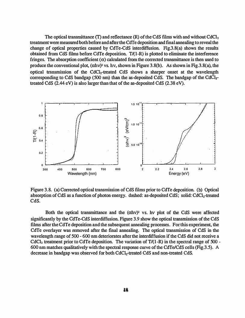
The optical transmittance (T) and reflectance (R) of the CdS films with and without CdCl2treatment were measured both before and after the CdTe deposition and final annealing to reveal the change of optical properties caused by CdTe-CdS interdiffusion. Fig.3.8(a) shows the results obtained from CdS films before CdTe deposition. T/(1-R) is plotted to eliminate the interference fringes. The absorption coefficient (a) calculated from the corrected transmittance is then used to produce the conventional plot, (ahv)2 vs. hv, shown in Figure 3.8(b). As shown in Fig.3.8(a), theoptical transmission of the CdC12-treated CdS shows a sharper onset at the wavelength corresponding to CdS bandgap (500 nm) than the as-deposited CdS. The bandgap of the CdClztreated CdS (2.44 e V) is also larger than that of the as-deposited CdS (2.38 e V).
0.8
I 0.6 �
I ...- i � 0.4 1 !
0.2
0 300 400 500 600 700 800
Wavelength (nm)
1 .5 1 01 1
N
E' 1 .0 1 0 1 1 (.) > �
"'.--... ;>
-§ 5 0 1 010 '-" .
0 2 2.2
,· / //
/ I
l !
l /
2.4 2.6 2.8 3 Energy (eV)
Figure 3.8. (a) Corrected optical transmission of CdS films prior to CdTe deposition. (b) Optical absorption of CdS as a function of photon energy. dashed: as-deposited CdS; solid: CdC12-treated CdS.
Both the optical transmittance and the (ahv)2 vs. hv plot of the CdS were affectedsignificantly by the CdTe-CdS interdiffusion. Figure 3.9 show the optical transmission of the CdS films after the CdTe deposition and the subsequent annealing processes. For this experiment, the CdTe overlayer was removed after the final annealing. The optical transmission of CdS in the wavelength range of 500 - 600 nm deteriorates after the interdiffusion if the CdS did not receive a CdCl2 treatment prior to CdTe deposition. The variation of T/(1-R) in the spectral range of 500 -
600 nm matches qualitatively with the spectral response curve of the CdTe/CdS cells (Fig.3.5). A decrease in bandgap was observed for both CdC12-treated CdS and non-treated CdS.

I l I
l
0.8
- 0.6 0:::
• ......
� o . .c
0.2
( a )
300 4 00 500 600 700 Wavelength (nm}
800
� E , .(.) 1 .0 1 0 >Q.l
-
( b )
2 2 .2
' /
'
2 4 2 6
Energy (eV} 2 .8
Figure 3.9. (a) Corrected optical transmission of CdS films after CdTe/CdS interdiffusion. (b) ( ahv)2 vs. hv plot of CdS after CdTe/CdS interdiffusion. dashed: as-deposited CdS; solid: CdC12-
treated CdS.
Fig. 3.10 shows the photoluminescence spectra of the CdTe/CdS films. For films prepared with CdC12-treated CdS, two peaks at 2.54 eV and 2.08 eV, corresponding to a near band gap transition and a deep transition of pure CdS, were observed. For films prepared with as-deposited CdS, only a broad peak, at 1 .74 eV energy, was observed. This transition is characteristic of the CdSt.yTey ternary phase [13] and is presumably related to deep levels introduced by Te in CdS. The photoluminescence results therefore confirm the results obtained fromXRD, i.e., CdCl2-treated CdS remains pure CdS while non-treated CdS is fully converted to ternary phase during the final annealing step.
19
c ::::l
-e �
6000
� 4000 ·u;c Q)
..... c
_J 0.. 2000
1 .6 1 .8 2 2.2 Energy (eV)
2.537 eV
2.4 2.6
Figure 3.1 0. Photoluminescence spectra of CdT e/CdS films prepared with as-deposited (solid line) and CdCb-treated CdS (open circles).
2Q
4. Study of ZnTe:Cu Back Contacts on CdTe/CdS Thin Film Solar Cells
The formation of stable, low-resistance contacts to p-type CdTe is critical for the achievement of high efficiency and long-term stability of CdTe thin-film solar cells. Because of the rather high ionization energy of CdTe and the difficulty of achieving high doping levels in p-type CdTe, a low-resistance ohmic contact cannot be formed by a simple metallization. Chemical reactions between CdTe and some of the high work function metals (e.g., Au) also make it difficult to form a stable ohmic contact by metal evaporation. ZnTe, which is expected to have a small valence band discontinuity with CdTe and can be doped degenerately with Cu, has been used as an intermediate layer between the high-resistivity CdTe and the metal contact [14,15]. Incorporation of a thermally evaporated Cu-doped ZnTe contact in CdTe/CdS cells yielded an efficiency of 11.2% [14,15], a record efficiency for thin-film solar cells at that time. Subsequently, other groups have investigated the deposition and properties ofZnTe thin films in relation to their application in thinfilm CdTe solar cells [16-18].
We studied the effects ofCu concentration, ZnTe:Cu layer thickness, ZnTe post-deposition annealing temperature, and contact material to the ZnTe on the photovoltaic performances of CdTe/CdS solar cells. ZnTe films doped with Cu were deposited by vacuum evaporation. The vacuum system had a base pressure of 1 x 1 � torr and was partitioned into two sections: one for a ZnTe powder source (99.999%, Johnson-Matthey) and the other for a Cu source (99.9999%, Johnson-Matthey). The ZnTe and Cu deposition rates were measured by separate thickness monitors. The typical deposition rates of the ZnTe were 5-10 Als. The deposition rate of the Cu was adjusted to a value between 0 and 0.2 Als to obtain the desired Cu atomic concentration in the ZnTe, varying between 4 and 10%. During vacuum deposition, the substrates were held at room temperature. The ZnTe:Cu layer thickness was varied from 400 to 1500 A. Post-depositionannealing was performed in a N2 environment. A strip heater was used for the annealing and was composed ofMo sheet metal as the heating element and a graphite block as the sample holder. This system reached temperatures above 400oC in less than 1.5 min and cooling from 400oC to 200°C took approximately 2 min. The solar cells were completed by evaporating metals on the annealed ZnTe/CdTe/CdS films. Three types of metals were used in this study to form the fmal metal contact to the ZnTe: Au, Ni, and Co.
4.1. Optimization of the ZnTe:Cu Layer and Its Processing Conditions
Table 4.1 shows the dependence of ZnTe/CdTe/CdS cell performances on the Cu concentration in the Zn Te fllms. Both V oc and J sc (not shown iii the table) are relatively independent of the Cu concentration over a wide range (from 4.3 to 7.5 at. % ). The fill factor (FF) was also lessaffected when the Cu concentration varied from 4.3 to 6.3 at. % . At higher Cu concentrations (7 .0, 7.5 at. % ), the fill factor decreased. The highest device performance was achieved at a Cu concentration of 5.4 at. %. The lack of Cu concentration dependence of the cell performance is certainly beneficial for large scale production.
21

Table 4.1. Effect of Cu concentration in ZnTe on Au/ZnTe/CdTe/CdS cell performances.
Cu concentration (at. %) Voc (V) IF(%)
4.3 0.76 0.70 5.1 0.71 0.70 5.4 0.77 0.73 6.3 0.75 0.70 7.0 0.73 0.63 7.5 0.75 0.66
The effects ofZnTe post-deposition annealing temperature on cell performances are shown in Table 4.2 for ZnTe/CdTe/CdS cells fabricated with both Au and Ni as the final metal contact to ZnTe. For both Au- and Ni-contacted cells, the highest fill factor was obtained for an annealing temperature of 168°C. Cells annealed at higher temperature (185°C) show lower fill factors. We have also investigated higher annealing temperatures. However, cells with good efficiencies were only obtainable at annealing temperatures below 200°C, even though ZnTe films with improved electrical and structural properties can be obtained at higher annealing temperatures [19]. This is possibly caused by degradation of the CdTe/CdS junction or reactions between CdTe and ZnTe at high annealing temperatures.
A significant difference in cell performance was observed when different metals were �sed as the final metal contactto ZnTe. The open-circuit photovoltage ofthe cells is critically dependent on the processing conditions ifNi was used as the contact metal to ZnTe. In many cases, V ocoften decreases after Ni deposition. In contrast, deposition of Au on the ZnTe/CdTe/CdS structure leads to consistent improvement of V oc· In collecting the data shown in Table 4.2, the Au- and Nicontacted cells were fabricated side-by-side on the same piece ofZnTe/CdTe sample. Only the final metallization step is different. Cells made with Au/ZnTe show consistently higher V oc than those with Ni contacts. The series resistances are comparable in both cases. The difference in FF originates mainly from the difference in V oc· Cells were also fabricated using Co as the contact metal to ZnTe, the cell performances were similar to those of Ni-contacted cells.
Table 4.2. Effect of ZnTe annealing temperature and back contact metal on cell performances. The Cu concentration in ZnTe was 5.5 at. %.
Back Contact Annealing temperature (<C) V oc (V) 1..: (mA/cm2) FF (%) Eff.(%)
155 0.77 21.6 0.72 11 .9 Au 168 0.77 21.4 0.73 12.1
185 0.76 20.2 0.68 10.4
155 0.65 22.8 0.65 10.5 Ni 168 0.68 23.1 0.70 11.1
185 0.70 22.4 0.67 10.5
22
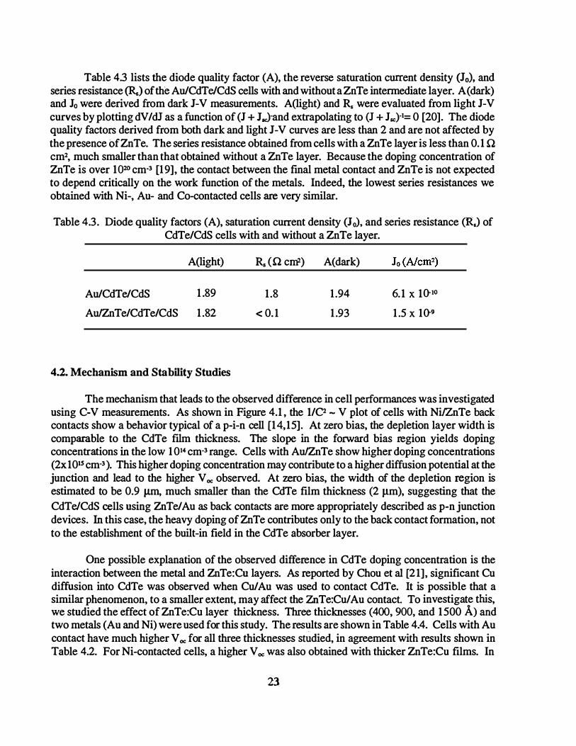
Table 4.3 lists the diode quality factor (A), the reverse saturation current density (Jo), andseries resistance (R) of the Au/CdTe/CdS cells with and without aZnTe intermediate layer. A( dark) and Jo were derived from dark J-V measurements. A(light) and R, were evaluated from light J-Vcurves by plotting dV/dJ as a function of (J + 1.,,)-and extrapolating to (J + Jsc)-1= 0 [20]. The diodequality factors derived from both dark and light J-V curves are less than 2 and are not affected by the presence ofZnTe. The series resistance obtained from cells with a ZnTe layer is less than 0.1 Q cm2, much smaller than that obtained without a ZnTe layer. Because the doping concentration of ZnTe is over 1020 cm-3 [19], the contact between the final metal contact and ZnTe is not expected to depend critically on the work function of the metals. Indeed, the lowest series resistances we obtained with Ni-, Au- and Co-contacted cells are very similar.
Table 4.3. Diode quality factors (A), saturation current density (J o). and series resistance (R.) ofCdTe/CdS cells with and without a ZnTe layer.
A(light)
Au/CdTe/CdS 1.89
Au!ZnTe/CdTe/CdS 1.82
4.2. Mechanism and Stability Studies
R. (n cm2) A(dark)
1.8
< 0.1
1.94
1.93
6.1 X 1Q-10
1.5 X 1Q-9
The mechanism that leads to the observed difference in cell performances was investigated using C-V measurements. As shown in Figure 4.1, the 1/C2 - V plot of cells with Ni/ZnTe back contacts show a behavior typical of a p-i-n cell [14,15]. At zero bias, the depletion layer width is comparable to the CdTe film thickness. The slope in the forward bias region yields doping concentrations in the low 1014 cm-3 range. Cells with Au!ZnTe show higher doping concentrations (2x 1015 cm-3 ). This higher doping concentration may contribute to a higher diffusion potential at the junction and lead to the higher V oc observed. At zero bias, the width of the depletion region is estimated to be 0.9 J.Lm, much smaller than the CdTe film thickness (2 J.Lm), suggesting that the CdTe/CdS cells using ZnTe/Au as back contacts are more appropriately described as p-njunction devices. In this case, the heavy doping of ZnTe contributes only to the back contact formation, not to the establishment of the built-in field in the CdTe absorber layer.
One possible explanation of the observed difference in CdTe doping concentration is the interaction between the metal and ZnTe:Cu layers. As reported by Chou et al [21], significant Cu diffusion into CdTe was observed when Cu/ Au was used to contact CdTe. It is possible that a similar phenomenon, to a smaller extent, may affect the ZnTe:Cu/ Au contact. To investigate this, we studied the effect of ZnTe:Cu layer thickness. Three thicknesses (400, 900, and 1500 A) andtwo metals (Au and Ni) were used for this study. The results are shown in Table 4.4. Cells with Au contact have much higher V oc for all three thicknesses stUdied, in agreement with results shown in Table 4.2. For Ni-contacted cells, a higher V oc was also obtained with thicker ZnTe:Cu films. In
23

�Ni/ZnTe/CdTe/Cd ' ·,
�Au/ZnTe/CdTeic�s '
\ ·,,
O b===�==�==�==�==�==�==� -3 -2.5 -2 - 1 .5 -1
BIAS (V) -0.5 0 0.5
Figure 4.1. l/C2 vs V plotsof CdS/CdTe/ZnTe cells using Au and Ni as contact metals to ZnTe.
terms of the CdTe doping concentration, a clear trend was observed for the ZnTe:Cu/ Au-contacted cells: higher CdTe doping concentrations were obtained with thicker ZnTe:Cu films. This can be explained by the possible Cu-diffusion that results from interactions between back contact metal and ZnTe:Cu layers. More significant Cu-diffusion may be expected from thicker ZnTe:Cu films because of the larger amount ofCu that is present. The CdTe doping concentration in Ni-contacted cells is much lower than that of Au-contacted cells. It does not show a significant variation with ZnTe thickness.
Table 4.4. V oc and its stability of CdS/CdTe/ZnTe cells and the doping concentration deduced from dark C-V curves.
Sample
6411 Au 6412 Au 6413 Au
6411 Ni 6412 Ni 6413 Ni
ZnTe thickness (A)
400 900
1500
400 900
1500
V oc (as-prepared) (mV)
741 738 750
653 697 702
24
V oc (9 days later) Doping density (mV) (cm-3)
762 2.8*1014 750 4.4*1014 752 6.2*1014
692 0.74*1014 710 0.76*1014 708 L2*1Q14
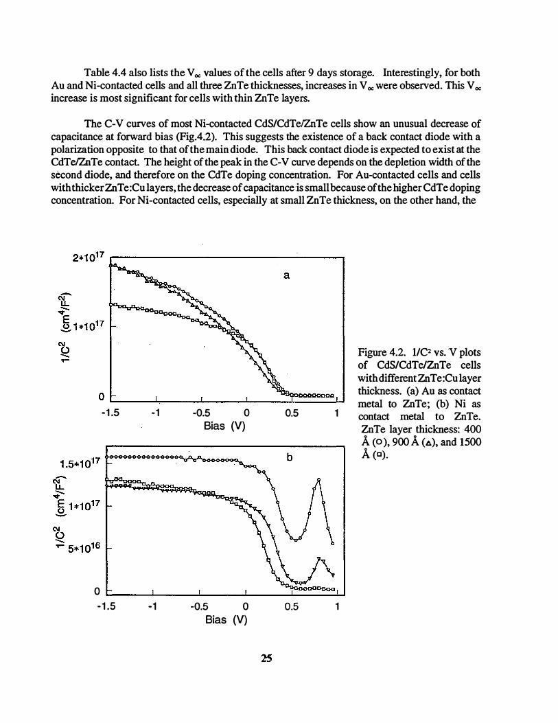
Table 4.4 also lists the V oc values of the cells after 9 days storage. Interestingly, for both Au and Ni-contacted cells and all three ZnTe thicknesses, increases in V oc were observed. This V oc
increase is most significant for cells with thin ZnTe layers.
The C-V curves of most Ni-contacted CdS/CdTe/ZnTe cells show an unusual decrease of capacitance at forward bias (Fig.42). This suggests the existence of a back contact diode with a polarization opposite to that of the main diode. This back contact diode is expected to exist at the CdTe!ZnTe contact. The height of the peak in the C-V curve depends on the depletion width of the second diode, and therefore on the CdTe doping concentration. For Au-contacted cells and cells with thicker Zn Te:Cu layers, the decrease of capacitance is small because of the higher CdTe doping concentration. For Ni-contacted cells, especially at small ZnTe thickness, on the other hand, the
o c_ __ �---L--�--���� -1 .5 -1 -0.5 0
Bias (V) 0.5 1
0 �----------�----------�---------------�----------�---------------� -1 .5 -1 -0.5 0
Bias (V) 0.5 1
Figure 4.2. 1/C2 vs. V plots of CdS/CdTe/ZnTe cells with different ZnTe:Cu layer thickness. (a) Au as contact metal to ZnTe; (b) Ni as contact metal to ZnTe. ZnTe layer thickness: 400 A (o ), 900 A <�>. and tsoo A (c).
CdTe doping concentration is small, leading to a large decrease of the capacitance. The existence of the back contact diode may be partially responsible for the lower V oe in the Ni-contacted cells. It also implies that even though the valence band offset at ZnTe/CdTe interface is expected to be small, it may not be negligible in certain cases.
We have noticed an interesting feature during our studies of the CdS/CdTe/ZnTe system. The lowest series resistance, with dV /dJ @V oe values in the range of 3.5- 3.8 O-cm2, was very often obtained with cells that showed lower V oe· For cells with high V oe. the value of dV/dJ@Voe is often slightly higher, around 3.8 - 4.4 n-cm2• This variation of V oe and series resistance in opposite directions results in comparable fill factors (- 0. 70) in both cases. This trend was first noticed in our study of different metal contacts (e.g., Au and Ni) on ZnTe. Recently, we also see such a trend for CdS/CdTe/ZnTe cells made with different batches of CdTe films using the same metal contact. Capacitance-voltage measurements indicate that the doping concentration of the CdTe layer near the back contact is lower for cells that exhibit low contact resistance. This may be another evidenceof a small valence band offset (- 0.2 eV) at the CdTe/ZnTe interface.
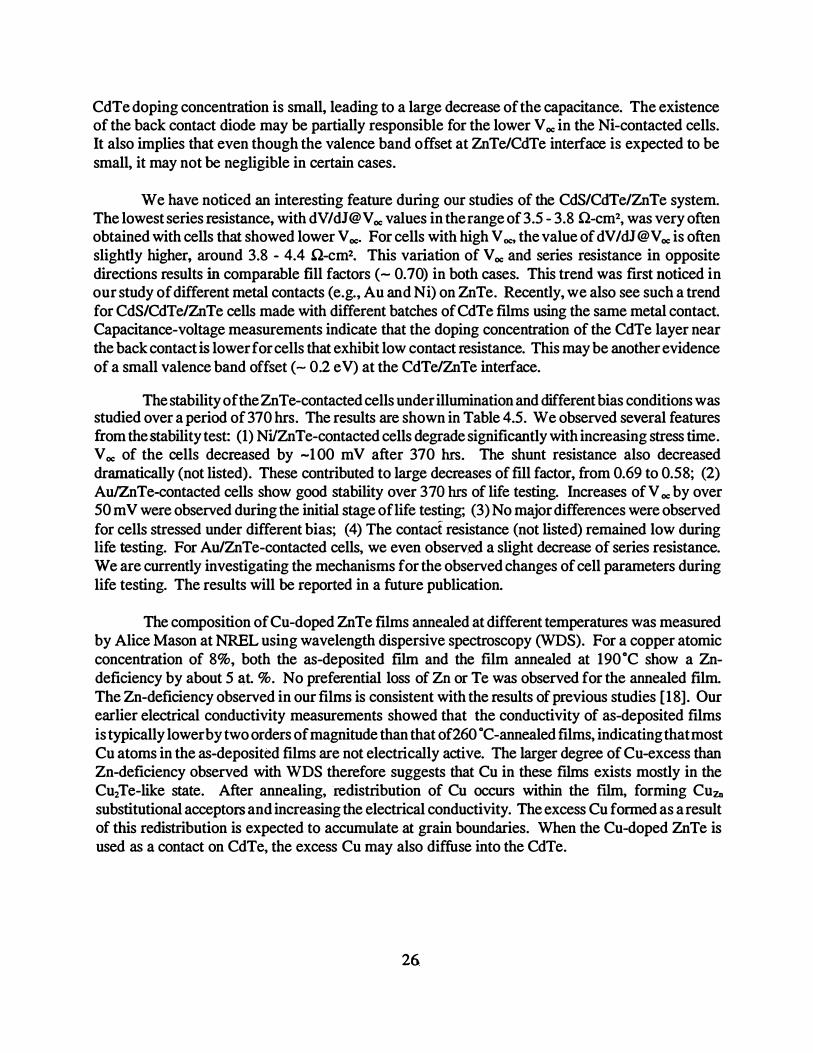
The stability of the Zn Te-contacted cells under illumination and different bias conditions was studied over a period of 370 hrs. The results are shown in Table 4.5. We observed several features from the stability test: (1) Ni!ZnTe-contacted cells degrade significantly with increasing stress time. V oe of the cells decreased by -100 m V after 370 hrs. The shunt resistance also decreased dramatically (not listed). These contributed to large decreases of fill factor, from 0.69 to 0.58; (2) Au/ZnTe-contacted cells show good stability over 370 hrs of life testing. Increases ofV oe by over 50 m V were observed during the initial stage oflife testing; (3) No major differences were observed for cells stressed under different bias; (4) The contact resistance (not listed) remained low during life testing. For Au/ZnTe-contacted cells, we even observ,ed a slight decrease of series resistance. We are currently investigating the mechanisms for the observed changes of cell parameters during life testing. The results will be reported in a future publication.
The composition of Cu-doped ZnTe films annealed at different temperatures was measured by Alice Mason at NREL using wavelength dispersive spectroscopy (WDS). For a copper atomic concentration of 8%, both the as-deposited film and the film annealed at 190oC show a Zndeficiency by about 5 a,t. %. No preferential loss of Zn or Te was observed for the annealed film. The Zn-deficiency observed in our films is consistent with the results of previous studies [18]. Our earlier electrical conductivity measurements showed that the conductivity of as-deposited films is typically lower by two orders of magnitude than that of260 °C-annealed films, indicating that most Cu atoms in the as-deposited films are not electrically active. The larger degree of Cu-excess than Zn-deficiency observed with WDS therefore suggests that Cu in these films exists mostly in the Cu2Te-like state. After annealing, redistribution of Cu occurs within the film, forming CuZn substitutional acceptors and increasing the electrical conductivity. The excess Cu formed as a result of this redistribution is expected to accumulate at grain boundaries. When the Cu-doped ZnTe is used as a contact on CdTe, the excess Cu may also diffuse into the CdTe.
26,
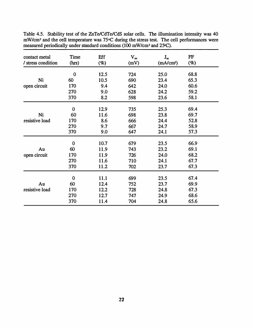
Table 4.5. Stability test of the ZnTe/CdTe/CdS solar cells. The illumination intensity was 40 mW/cm2 and the cell temperature was 75oC during the stress test. The cell performances were measured periodically under standard conditions (100 mW/cm2 and 25oC).
contact metal Time Eff Voc Isc FF I stress condition (hrs) (%) (mV) (mA/cm2) (%)
0 12.5 724 25.0 68.8 Ni 60 10.5 690 23.4 65.3
open circuit 170 9.4 642 24.0 60.6 270 9.0 628 24.2 59.2 370 8.2 598 23.6 58.1
0 12.9 735 25.3 69.4 Ni 60 11.6 698 23.8 69.7
resistive load 170 8.6 666 24.4 52.8 270 9.7 667 24.7 58.9 370 9.0 647 24.1 57.3
0 10.7 679 23.5 66.9 Au 60 11.9 743 23.2 69.1
open circuit 170 11.9 726 24.0 68.2 270 11.6 710 24.1 67.7 370 11.2 702 23.7 67.3
0 11.1 699 23.5 67.4 Au 60 12.4 752 23.7 69.9
resistive load 170 12.2 728 24.8 67.3 270 12.7 747 24.9 68.6 370 11.4 704 24.8 65.6
27
5. Optimization of Solar Cell Structure
5.1 Effect of CdS thickness
We investigated the effect of CdS thickness on the photovoltaic performance of CdTe/CdS cells. The results are shown in Table 5.1 . As expected, J sc of the cells decreases monotonically withincreasing CdS thickness because of the increased absorption in the window layer. However, high V oc and efficiencies were obtained only for CdS thicknesses above 1500 A. Cells with very thin(700 A) CdS exhibit low efficiency, caused mainly by a low V oc· The highest efficiency wasobtained for a CdS thickness of 1 500 A.
Table 5.1 . Effect of CdS thickness on the photovoltaic performance of CdTe/CdS cells.
CdS Voc Jsc FF 11 Rsh thickness (mV) (mA/cm2) (%) (%) (0-cm2)
100 A 645 24.0 54.0 8.3 550 t5oo A 780 23.0 72.0 12.9 1800 2300 A 775 22.0 69.0 12.0 2500 2500 A 765 21 .5 70.0 1 1 .6 2200
The inferior cell performance observed with thin CdS is caused by the high consumption of CdS during the fmal annealing of CdTe/CdS films. Our XRD studies and direct measurements with surface profilometry indicated that a decrease of CdS film thickness of -600 A for the CdTe film thickness used (3.4 J.lm). This high CdS consumption caused by CdTe-CdS interdiffusion is expected to play a critical role in determining the smallest CdS thickness that can be employed in CdTe/CdS solar cells fabricated with electrodeposition. Because electrodeposited CdTe films, in its as-deposited state, have much smaller grains ( -0. 1 - 0.2 J.lm) than films formed by high
temperature processes (e.g., close-spaced sublimation}, the diffusion of S into electrodeposited CdTe is more significant in the former. Based on our measurement, a CdS thickness of 1200-1300 A isestimated to be the lower limit for fabricating CdTe/CdS solar cells using electrodeposition.
5.2 Effect of CdTe thickness
Table 5.2 shows the dependence of cell parameters on CdTe thickness. The CdTe thickness was varied from 2.2 mm to 5.3 J.lm. A CdTe thickness of 2.2 J.lm, typical of most studies using electrodeposited CdTe, yielded V oc values in the low 700 m V range. An increase of CdTe thickness to 3.4 J.lm lead to a significant improvement in V oc• by -70 m V. The highest V oc obtained at this
CdTe thickness exceeded 800 m V. Further increase of the CdTe layer thickness to 5.3 J.lm, however, resulted in low shunt resistance and low efficiencies of the cells.
28

Table 5.2. Effect of CdTe thickness on cell performances.
CdTe Voc Jsc R.t. thickness (mV) (rnNcm2) (il-cm2)
2.2 J.Lm 708 22.9 890 3.4 J.lm 775 22.8 800
5.3 J.lm 757 22.8 210
SEM measurements were performed on CdTe films of various thicknesses after CdCh treatment and annealing. The average CdTe grain size was larger for the thicker CdTe films (Figure 5. 1). This increase of grain size may explain the improved V oc obtained with 3.4 Jlm CdTe. The
deteriorated cell performance obtained with 5.3 J.lill CdTe is caused by the poor adhesion of CdTeon the substrate and the formation of shunting paths in the CdTe layer during the post-deposition annealing.
(a) (b)
Figure 5 . 1 . SEM images of CdTe films after CdCh-treatment and 41 O>C-annealing. The CdTe film thickness was (a) 2.2 J.lm and (b) 3.4 Jlffi.
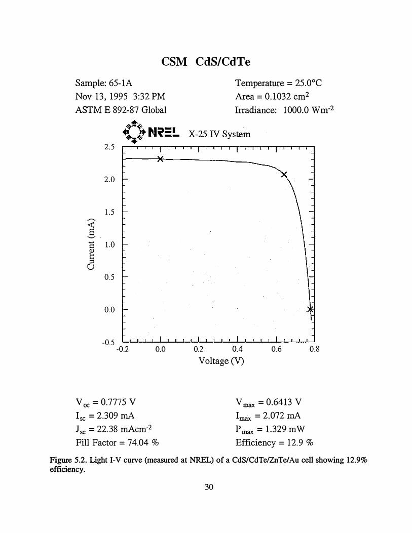
Our systematic investigation and optimization of the processing conditions has lead to consistent improvement of the efficiency of CdTe/CdS cells we fabricate. The light I-V curve of a CdS/CdTe!ZnTe cell. which yielded a V oc of 0.778 V, a J sc of 22.4 mA/cm2, a FF of 74.0%, dodan efficiency of 12.9%, is shown in Fig. 5.2. The spectral response of this cell is shown in Fig. 5.3. In terms of individual parameters, we have obtained V oc values of over 0.8 V, and FF values of76%from other cells.
29
CSM CdS/CdTe Sample: 65- 1 ANov 1 3 , 1 995 3:32 PM
ASTM E 892-87 Global
2.5
2.0
1 .5 �
@'--" . .... 1 .0 t::: <I) t:: �
u 0.5
0.0
-0.5 -0.2
v oc = 0.7775 vIsc = 2.309 rnA
0.0
J sc = 22.38 mAcm·2
Fill Factor = 74.04 %
Temperature = 25.0°C
Area = 0. 1 032 cm2
Irradiance: 1 000.0 Wm-2
0.2 0.4 Voltage (V)
0.6 0.8
V max = 0.6413 V
Imax = 2.072 rnAP max = 1 .329 mW
Efficiency = 1 2.9 %
Figure 5.2. Light 1-V curve (measured at NREL) of a CdS/CdTe!ZnTe/Au cell showing 12.9%efficiency.
30

CSM CdS/CdTe Sample: 65-1 (C) Temperature = 25 :0°C
Device Area = 0. 1 02 cm2 ·· Oct 3 1 , 1995 8:58 AM
.,......,. �'-"
» (.) � Q) ...... (.)
� 4-i � sE§;:=j
ClQ) >
".:::::1 ro -Q)
�
100
80
60
40
20
0
.... ·� 1'"'� ··�=· � .... � I' �-- Filter QE System..
� � @ � � � � � 1� Wavelength (nm)
Light Bias = 1 .000 rnABias Voltage = 0.00 V
Figure 5.3. Spectral response curve (measured at NREL) of a CdS/CdTe/ZnTe/Au cell showing 12.9% efficiency.
31

6. Summary
We have studied the structural and electrical properties of chemical-bath-deposited CdS thin films and the CBD growth mechanisms. We demonstrated that the measurement of refractive index as a function of deposition time provides a simple way to determine the transition point from compact layer growth to porous layer growth. The crystalline phase of as-deposited CdS was identified as cubic based on XRD analysis of the thin films and powders.
We investigated the CdTe-CdS interdiffusion and the effect of CdCh treatment of CdS fllms on the photovoltaic performances. Both XRD and photoluminescence measurements indicated amajor difference in the extent of Te diffusion into CdS for the two types of CdS films: Fullconversion ofCdS into CdS1.yTey was observed for films prepared with as-deposited CdS, while the formation of the ternary phase was below the detection limit for films prepared with CdClz-treated CdS. The difference in interdiffusion leads to differences in optical transmission of CdS films and spectral response of CdTe/CdS solar cells. An increase of 2.7 mA/cm2 in Jsc was obtained usingCdClz-treated CdS.
·
We have studied the formation of back contact to the CdTe cells using Cu-doped ZnTe. The effects of Cu concentration, ZnTe post-deposition annealing temperature, and the types of metalsused to contact ZnTe on solar cell performances were studied. A Cu concentration of 5.4 at. %, a ZnTe post-deposition annealing temperature of 17QoC, and Au metal contact on ZnTe were found to yield the highest cell performances. The series resistance of the CdTe/CdS cells was reduced significantly by the introduction of the ZnTe layer. Fill factors greater than 0.70 were consistently obtained, with the highest value reaching 0.76.
The effect of CdTe and CdS thickness on the photovoltaic performance of the resulting cells was studied. We found that an increase in the CdTe thickness from 2 Jlm to 3.5 Jlm lead to a
consistent improvement in V oc by 40-60 m V. The shunt resistance of the cells was also increased. In terms of CdS layer thickness, the most efficient cells were obtained with 1500 A CdS. For cellsmade with thinner CdS, both V oc and shunt resistance were low because of the significant consumption of CdS during CdS-CdTe interdiffusion.
Our systematic investigation and optimization of the processing conditions have resulted in consistent improvement of the device efficiency of our CdTe solar cells. Our best CdTe/CdS cell exhibited a V oc of 0.778 V, a Jsc of 22.4 mA/cm2, an FF of 74.0%, and an efficiency of 12.9%(verified at NREL).
7. Acknowledgements
We thank the scientists at the National Renewable Energy laboratory (NREL) for vanous measurements, especially Richard Matson for SEM and EBIC, Halden Field, Keith Emery, and Don Dunlavy for light J-V and spectral-response measurements, Amy Franz and David Niles for AES and XPS measurements, and Alice Mason for electron probe microanalysis. We thank the NREL CdTe team members: Peter Sheldon, David Albin, Xiaonan Li, Tim Gessert, and Ramesh Dhere for many helpful discussions and experimental help. We thank Brian McCandless of the Institute of Energy Conversion, University of Delaware for investigation of Co-diffused contact on our CdTe films. The investigation of the effect of CdS film thickness on cell performances was part of a coordinated effort of the Thin Film Photovoltaic Partnership team. Chris Ferekides of University of South Florida provided Sn02-coated glass substrates and James Sites and Jennifer Granata of Colorado State University performed the cell characterization for this team activity. Finally, we thank Kenneth Zweibel and Bolko von Roedern of NREL for many helpful discussions and encouragement.
8. References
1 . I. Kaur, D.K. Pandya, and K.L. Chopra. Solid State Science and Technology 127, 943:(1980).
2. D. Lincot and R.O. Borges, J. Electrochem. Soc. 139, 1880 (1992).
3. R.O. Borges and D. Lincot, J. Electrochem. Soc. 140, 3464 (1993).
4. J.M. Dona and J. Herrero, J. Electrochem. Soc. 139, 2810 (1992).
5. T.L. Chu, S.S. Chu, N. Schultz, C. Wang, and C.Q. Wu, J. Electrochem. Soc. 139, 2443 (1982).
6. L. Hernandez, 0. Melo, 0. Zelaya-Angel, and R. Lozada-Morales, J. Electrochem. Soc. 141,3238 (1994).
7. H. Uda, S. Ikegami, and H. Sonomura, J. Appl. Phys. 129, 30 (1990).
8. W J. Danaker, L.E. Lionc, and G.C. Morris, Sol. Energy Mater. 12, 137 (1985)
9. 0. de Melo, L. Hernandez, 0. Zelaya-Angel, R. Lozada-Morales, and M. Becerril, Appl. Phys. Lett. 65, 1278 (1994)
10. R.W. Birkmire, I.E. Phillips, W.A. Buchanan, S.S. Hegedus, B.E. McCandless, W.N.Shafarman, and T.A. Yokimcus, "Processing and Modeling Issues for Thin-Film Solar Cell Devices", Annual Report to NREL under Subcontract No. X-AV-131 70-01 (1994).
1 1 . G.C. Morris and S.K. Das, Proceedings of the 23rd Photovoltaic Specialists Conference (IEEE, New York, 1993) p. 469.
33
12. B .E. McCandless and S.S. Hegedus, Proceedings of the 22nd Photovoltaic Specialists Conference (IEEE, New York, 1991) p. 967.
13. 0. de Melo, M. Melendez-Lira, I. Hemandez-Calderon, L. Banos, and A. Morales-Acevedo,Proceedings of the First World Conference on Photo voltaic Energy Conversion (IEEE, New York, 1994) p.369.
14. P.V. Meyers, "Polycrystalline Cadmium Telluride n-i-p Solar Cell," Annual Report to SERIunder Subcontract No. ZL-7-06031-2 (1988).
15. P.V. Meyers, "Polycrystalline Cadmium Telluride n-i-p Solar Cell," Final Report to SERI underSubcontract No. ZL-7-06031-2 (1990).
16. A. Mondal, R.W. Birkmire, and B.E. McCandless, Proceedings of the 22nd IEEE PhotovoltaicSpecialist Conference (IEEE, New York, 1991) p. l 1 26.
17. T.A. Gessert and T.J. Coutts, 12th NREL Photovoltaic Review, AlP Conference Proceedings306, edited by Rommel Noufi and Harin S. Ullal (AlP, New York,1994) p.345.
1 8. T.A. Gessert, X. Li, T.J. Coutts, A.R. Mason, and R.I. Matson, J. Vac. Sci. Technol. A12, 1501(1994).
19. L. Feng, D. Mao, J. Tang, R.T. Collins, and J.U. Trefny, J. Electronic Materials (1996, in print).
20. J.R. Sites, "Role ofPolycrystallinity in CdTe and CulnSe2 Photovoltaic Cells", Annual Reportto NREL under Subcontract XC-0-10046-1 (1992).
21 . H. C. Chou, A. Rohatgi, E.W. Thomas, S. Kamra, and A.K. Bhat, J. Electrochem. Soc. 142,254 (1995).
34
9. Appendices
9.1. Personnel
Many individuals contributed to this work. Their names, titles, and representative responsibilities are summarized below. Those who have been involved during just a portion of the project period are noted.
John U. Trefny, Professor of Physics: Project Coordinator.
Duli Mao, Research Assistant Professor: Photovoltaic Development.
Don L. Williamson, Professor of Physics: XRD, SAXS.
Reuben T. Collins, Professor of Physics: Electronic and Optical Properties of Semiconductors.
Thomas E. Furtak, Professor of Physics: Electrochemistry, Optical Properties.
Timothy R. Ohno, Assistant Professor of Physics: Surface Physics.
Lianghuan Feng, Visiting Professor, ZnTe Back Contact and Cell Fabrications, (02/94-06/95).
Yuming Zhu, Graduate Research Assistant: CdS Chemical Bath Deposition.
Wenjie Song, Graduate Research Assistant: CdTe Electrodeposition and Cell Optimization.
Jian Tang, Graduate Research Assistant: ZnTe Back Contact, Cell Fabrication, and Stability.
M. Hasan Asian, Graduate Student: Photoluminescence.
Esam Alarfaj, Graduate Student: Study of CdTe Film Properties.
Ahamed Alkaoud, Graduat Student: Transparent Conducting Oxide.
Troy Berens, Graduate Student: Copper Indium Diselenide Thin Film Solar Cells.
35
9.2. Publications
1 . "Effect of Annealing on Microstructure, Residual Stress, and Photovoltaic Characteristics of Electrodeposited CdTe Films", D. Kim, B. Qi, D.L. Williamson, and J.U. Trefny, Proc. 24th IEEE PVSC, 338 (1994).
2� "Polycrystalline Thin Film CdTe Solar Cells Fabricated by Electrodeposition", D. Kim, S. Pozder, Y. Zhu, and J.U. Trefny, Proc. 24th IEEE PVSC, 334 (1994).
3. "Interdiffusion in Polycrystalline Thin Film CdS/CdTe Solar Cells", D. Mao, L.H. Feng, Y.Zhu, J. Tang, W. Song, R. Collins, D.L. Williamson, and J.U. Trefny, 13th NREL PhotovoltaicProgram Review, AlP Conference Proceedings 353, edited by Harin S. Ullal and C. Edwin Witt,(AlP, New York, 1995) p.352.
4. "Effect of Annealing on Microstructure, Residual Stress, and Photovoltaic Characteristics ofElectrodeposited CdTe Films", B. Qi, D. Kim, D.L. Williamson, and J.U. Trefny, J. ofElectrochem. Soc. 143, 517 (1996).
5. "The Structural, Optical, and Electrical Properties of Vacuum Evaporated Cu-doped ZnTePolycrystalline Thin Films' , L.H. Feng, D. Mao, J. Tang, R.T. Collins, and J.U. Trefny, J. Electron. Materials, September issue, 1996 (in print).
6. "Effect of CdC12 Treatment of CdS Films on CdTe/CdS Solar Cells", W. Song, D. Mao, L. Feng,Y. Zhu, M.H. Asian, R.T. Collins, and J.U. Trefny, Proceedings of the Materials ResearchSociety Meeting, Thin Films for Photovoltaics and Related Device Applications, Spring 1996,(in print).
7. "Study of ZnTe:Cu Back Contacts on CdTe/CdS Thin Film Solar Cells", J. Tang, L. Feng, D.Mao, W. Song, Y. Zhu, and J.U. Trefny, ibid, (in print).
8. "Chemical Bath Deposition of CdS Thin Films: Growth and Structural Studies", Y. Zhu, D. Mao,D.L. Williamson, and J.U. Trefny, ibid, (in print).
9. "Study of ZnTe:Cu Back Contacts on CdTe/CdS Thin Film Solar Cells", J. Tang, D. Mao, L.Feng, W. Song, and J.U. Trefny, Proc. 25th IEEE PVSC, (in print).
1 0. "Fabrication ofCdTe Thin Film Solar Cells Using Electrode position", W. Song, D. Mao, Y. Zhu, J. Tang, and J.U. Trefny, Proc. 25th IEEE PVSC, (in print).
l J REPORT DOCUMENTATION PAGE Form Approved
OMB NO. 0704-0188 l Public reporting burden for this collection of information is estimated to average 1 hour per response, including the time for reviewin� instructions, searching existing data sources,
J gathering and maintaining the data needed, and completing and reviewinfc the collection of information. Send comments regardinfc t is burden estimate or any other aspect of this collection of information, .ncludi�g.
(su�ions for reduci� this burden, o Washington Headguarters Services, Directorate for In ��ation O�rations �'::tc Relfcrts, 1215 Jefferson
Davis Highway, Suite 1204, Arlin on, 'A 22202-4302, an to the Office of Management and Budget, Paperwork Reduction Project 0704-01 , Wash in on, C 20503. 1 . AGENCY USE ONLY (Leave blank) 2. REPORT DATE 3. REPORT TYPE AND DATES COVERED
April 1 997 Annual Subcontract Report, 20 March 1 995 - 1 9 March 1 996
J 4. TITLE AND SUBTITLE 5. FUNDING NUMBERSPolycrystalline Thin Film Cadmium Telluride Solar Cells Fabricated by Electrodeposiiton; Annual
l Technical Report, 20 March 1 995 -1 9 March 1 996 C: XAF-5-1 41 42-1 1
) s. AUTHOR(S) TA: PV704401
J.U. Trefny and D. Mao
("
PERFORMING ORGANIZATION NAME(S) AND ADDRESS(ES) 8. PERFORMING ORGANIZATION REPORT NUMBER
Department of Physics Colorado School of Mines Golden, Colorado 80401
) s. SPONSORING/MONITORING AGENCY NAME(S) AND ADDRESS(ES) 1 0. SPONSORING/MONITORING AGENCY REPORT NUMBER
National Renewable Energy Laboratory SR-520-21 927 I 1 6 1 7 Cole Blvd.
Golden, CO 80401 -3393 DE96014325
j 1 1 . SUPPLEMENTARY NOTES I NREL Technical Monitor: B. von Roedern
12a. DISTRIBUTION/AVAILABILITY STATEMENT 1 2b. DISTRIBUTION CODE
1 UC-1 263
113. ABSTRACT (Maximum 200 words)
The objective of this project is to develop improved processes for fabricating CdTe/CdS polycrystalline thin-film solar cells. Researchers used electrodeposition to form CdTe; electrodeposition is a non-vacuum, low-cost technique that is attractive for economic, large-scale
,I production. During the past year, research and development efforts focused on several steps that are most critical to the fabricating high-
) efficiency CdTe solar cells. These include the optimization of the CdTe electrodeposition process, the effect of pretreatment of CdS substrates, the post-deposition annealing of CdTe, and back-contact formation using Cu-doped ZnTe. Systematic investigations of these processing steps have led to a better understanding and improved performances of the CdTe-based cells. Researchers studied the
I structural properties of chemical-bath-deposited CdS thin films and their growth mechanisms by investigating CdS samples prepared at different deposition times; investigated the effect of CdCI2 treatment of CdS films on the photovoltaic performance of CdTe solar cells; studied Cu-doped ZnTe as a promising material for forming stable, low-resistance contacts to the p-type CdTe; and investigated the effect of CdTe and CdS thickness on the photovoltaic performance of the resulting cells. As a result of their systematic investigation and
j optimization of the processing conditions, researchers improved the efficiency of CdTe/CdS cells using ZnTe back-contact and electrodeposited CdTe. The best CdTe/CdS cell exhibited a Voc of 0.778 V, a Jsc of 22.4 mA/cm2, a FF of 74%, and an efficiency of 1 2.9%(verified at NREL). In terms of individual parameters, researchers obtained a Voc over 0.8 V and a FF of 76% on other cells.
1 4. SUBJECT TERMS 15. NUMBER OF PAGES
I 47 photovoltaics ; polycrystalline thin films ; cadmium telluride solar cells ; electrodeposition 16. PRICE CODE
1
1
7
. SECURITY CLASSIFICATION 1 8. SECURITY CLASSIFICATION 19. SECURITY CLASSIFICATION 20. LIMITATION OF ABSTRACT OF REPORT OF THIS PAGE OF ABSTRACT Unclassified Unclassified Unclassified UL )SN 7540-01 -280-5500 Standard Form 298 (Rev. 2-89)
Prescribed by ANSI Std. 239-18 298-102