TECHNOLOGY AND MANUFACTURING DAY - Intel …€¦ · · 2017-03-28TECHNOLOGY AND MANUFACTURING...
33
Leading at the edge TECHNOLOGY AND MANUFACTURING DAY
Transcript of TECHNOLOGY AND MANUFACTURING DAY - Intel …€¦ · · 2017-03-28TECHNOLOGY AND MANUFACTURING...

Leading at the edgeTECHNOLOGY AND MANUFACTURING DAY

TECHNOLOGY AND MANUFACTURING DAY
Intel Technology and Manufacturing Day 2017 occurs during Intel’s “Quiet Period,” before Intel announces its 2017 firstquarter financial and operating results. Therefore, presenters will not be addressing first quarter information duringthis year’s program.
Statements in this presentation that refer to forecasts, future plans and expectations are forward-looking statementsthat involve a number of risks and uncertainties. Words such as “anticipates,” “expects,” “intends,” “goals,” “plans,”“believes,” “seeks,” “estimates,” “continues,” “may,” “will,” “would,” “should,” “could,” and variations of such words andsimilar expressions are intended to identify such forward-looking statements. Statements that refer to or are based onprojections, uncertain events or assumptions also identify forward-looking statements. Such statements are based onmanagement’s expectations as of March 28, 2017, and involve many risks and uncertainties that could cause actualresults to differ materially from those expressed or implied in these forward-looking statements. Important factors thatcould cause actual results to differ materially from the company’s expectations are set forth in Intel’s earnings releasedated January 26, 2017, which is included as an exhibit to Intel’s Form 8-K furnished to the SEC on such date.Additional information regarding these and other factors that could affect Intel’s results is included in Intel’s SEC filings,including the company’s most recent reports on Forms 10-K, 10-Q and 8-K reports may be obtained by visiting ourInvestor Relations website at www.intc.com or the SEC’s website at www.sec.gov.
Disclosures

TECHNOLOGY AND MANUFACTURING DAY
STACY J. SMITHExecutive Vice PresidentManufacturing, Operations and Sales
Strategy overview

TECHNOLOGY AND MANUFACTURING DAY
4
How small is 14 nm?
41 1 1 11010010100
METER MILLIMETER MICROMETER NANOMETER
10100
Fly
7 mmMite
300 umVirus
100 nmBlood Cell
7 umSilicon Atom
0.24 nmMark
1.66 m
10
Transistor
14 nm1,600,000,000 nm 7,000,000 nm 300,000 nm 7,000 nm
TECHNOLOGY AND MANUFACTURING DAY
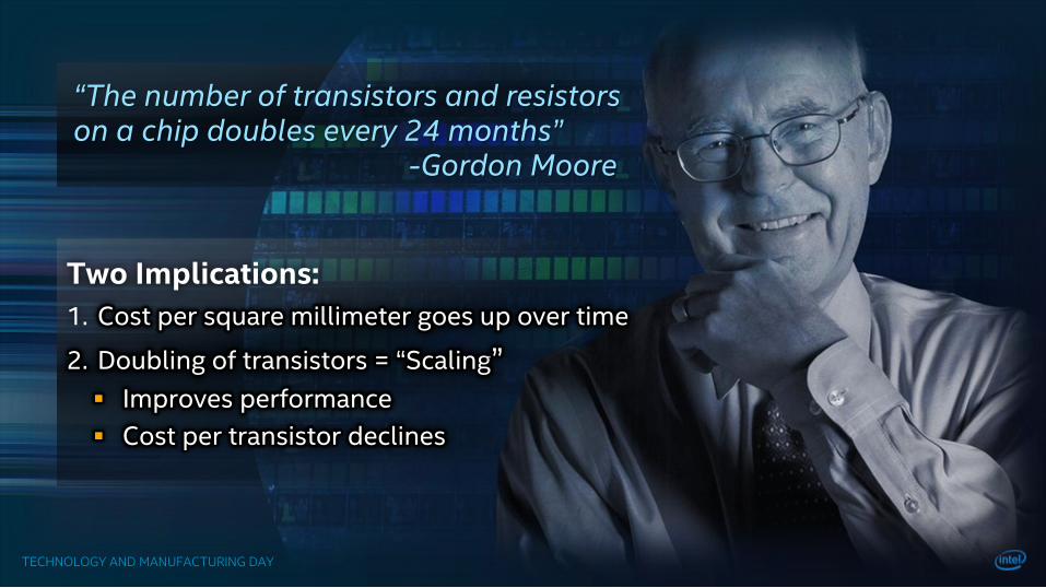
Two Implications:
1. Cost per square millimeter goes up over time
2. Doubling of transistors = “Scaling”
Improves performance
Cost per transistor declines
“The number of transistors and resistors on a chip doubles every 24 months”
-Gordon Moore
TECHNOLOGY AND MANUFACTURING DAY
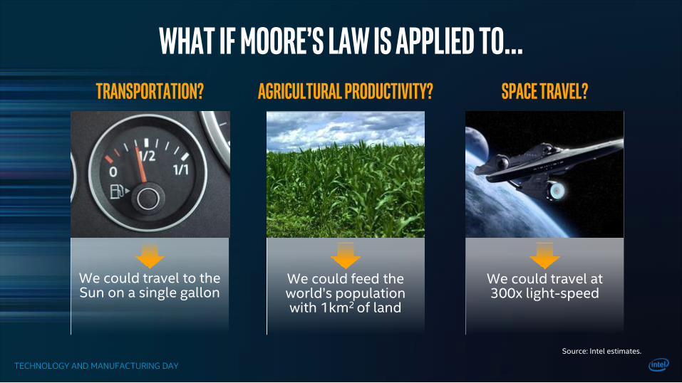
What if Moore’s Law is applied to…Space travel?
We could travel at 300x light-speed
Agricultural productivity?
We could feed the world’s population with 1km2 of land
Transportation?
We could travel to the Sun on a single gallon
Source: Intel estimates.

TECHNOLOGY AND MANUFACTURING DAY
Is Moore’s Law dead?

TECHNOLOGY AND MANUFACTURING DAY
Is moore’s law dead? NO!
Source: Intel10 nm and 7 nm forecasts are Intel estimates, based upon current expectations and available information.
mm2 / Transistor(log scale)
13
0 n
m
90
nm
65
nm
45
nm
32
nm
22
nm
14
nm
10
nm
7 n
m
$ / mm2
(log scale)
13
0 n
m
90
nm
65
nm
45
nm
32
nm
22
nm
14
nm
10
nm
7 n
m
13
0 n
m
90
nm
65
nm
45
nm
32
nm
22
nm
14
nm
10
nm
7 n
m
$ / Transistor(log scale)

TECHNOLOGY AND MANUFACTURING DAY
The time between nodes has lengthened…
Are you Getting the same Moore’s Law benefit?

TECHNOLOGY AND MANUFACTURING DAY
YES!Because we are getting
more scaling
TECHNOLOGY AND MANUFACTURING DAY
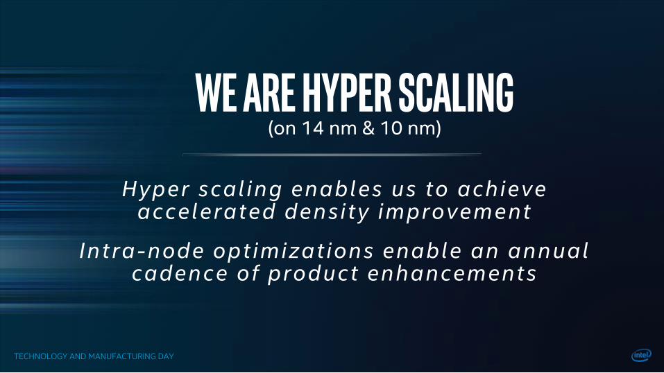
We Are Hyper Scaling(on 14 nm & 10 nm)
Hyper scaling enables us to achieve accelerated density improvement
Intra-node optimizations enable an annual cadence of product enhancements

TECHNOLOGY AND MANUFACTURING DAYSource: Intel
10 nm forecast is an Intel estimate, based upon current expectations and available information.
Microprocessor die area scaling
Hyper scaling delivers 0.46-0.43x die area scaling on 14 nm and 10 nm
100 mm2
45 nm 32 nm 22 nm 14 nm 10 nm
62 mm2
17.7 mm2
7.6 mm2
0.62x
Logic
SRAM
IO
100 mm2
Logic
SRAM
IO
100 mm2
Logic
SRAM
IO
100 mm2
Logic
SRAM
IO
100 mm2
Logic
SRAM
IO
0.43x
0.46x
0.62x
Area
38.4 mm2

TECHNOLOGY AND MANUFACTURING DAY
Moore’s Law Translates to Lower Product Costs22 nm & 14 nm Client Cost Curves
(Launch + 5 quarters)
*Q1’17 forecast is an Intel estimate, based upon current expectations and available information. Source: Intel
Q1'12 Q1'13 Q1'14 Q1'15 Q1'16 Q1'17F*
$
0
Broadwell
SkylakeHaswell
Ivybridge
Kabylake

TECHNOLOGY AND MANUFACTURING DAY
Moore's Law in action…PC CPU Weighted Average Cost Per Transistor ($/MTX)
(log scale normalized to 90 nm)
*Q1’17 forecast is an Intel estimate, based upon current expectations and available information. Source: Intel
$/MTX
90 nm
65 nm
45 nm
32 nm
22 nm
14 nm
TECHNOLOGY AND MANUFACTURING DAY
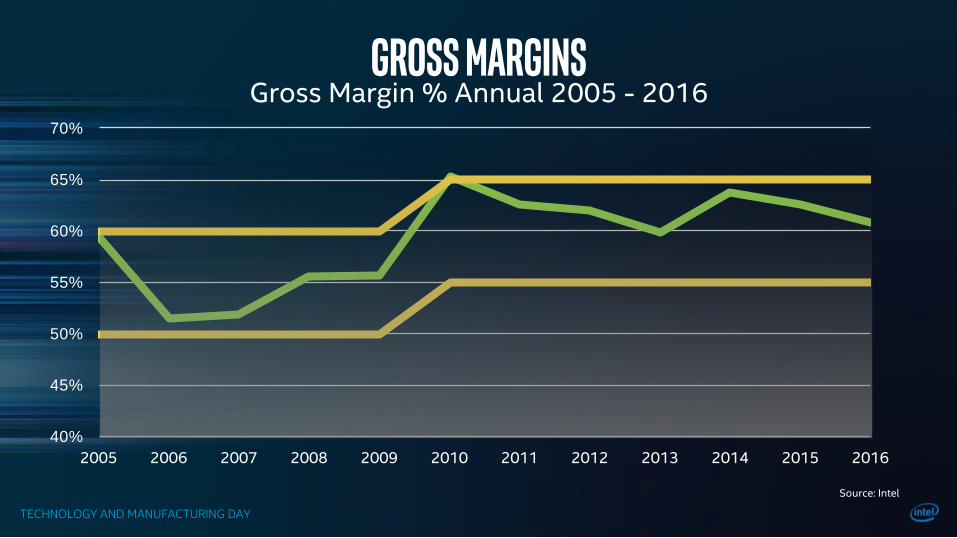
Gross MarginSGross Margin % Annual 2005 - 2016
Source: Intel
40%
45%
50%
55%
60%
65%
70%
2005 2006 2007 2008 2009 2010 2011 2012 2013 2014 2015 2016
TECHNOLOGY AND MANUFACTURING DAY
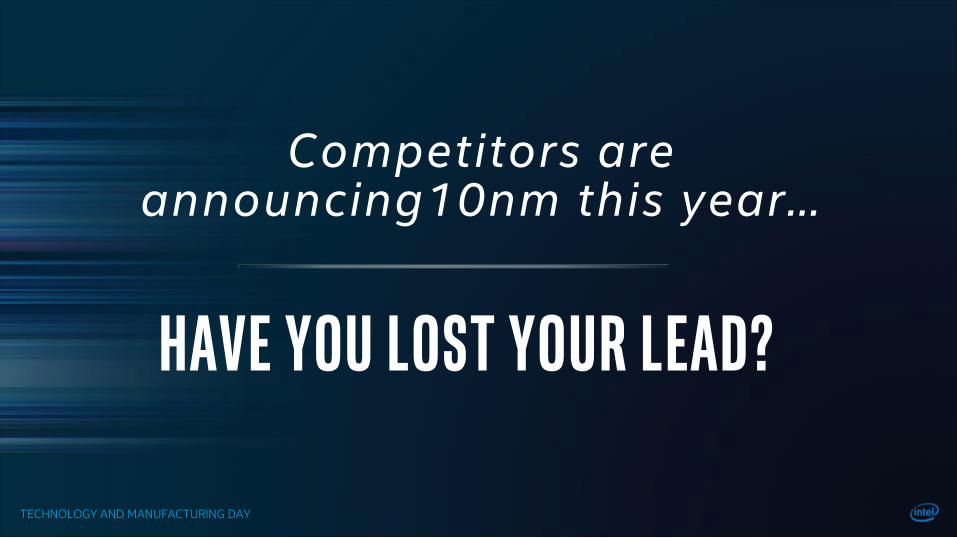
Competitors are announcing10nm this year…
Have you lost your lead?

TECHNOLOGY AND MANUFACTURING DAY
Have you lost your lead? No! 14 NM IS ~3 YEARS AHEAD
0.01
0.1
1
2007 2008 2009 2010 2011 2012 2013 2014 2015 2016 2017 2018 2019 2020
Logic
Area
(relative)
HVM Wafer Start Date
Others
Intel
45nm
22nm
14nm
10nm
32nm
40/45nm
10nm
28nm
20nm
14/16nm
3 years
Forecast*
*Forecast is an estimate, based upon current expectations and available information.
Source: Intel estimates.

TECHNOLOGY AND MANUFACTURING DAY
Our Scale

TECHNOLOGY AND MANUFACTURING DAY
Investment Required to Build & EquipA Leading Edge Wafer Factory
~$10bSource: Intel
TECHNOLOGY AND MANUFACTURING DAY
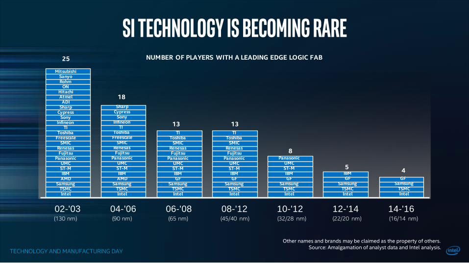
Si technology is becoming rare
Other names and brands may be claimed as the property of others.Source: Amalgamation of analyst data and Intel analysis.
02-'03 04-'06 06-'08 08-'12 10-'12 12-'14 14-'16
NUMBER OF PLAYERS WITH A LEADING EDGE LOGIC FAB25
18
13 13
8
5
TSMCIntel
SamsungGF
IBMST-MUMC
Panasonic
TSMCIntel
SamsungGF
IBM
(130 nm) (90 nm) (65 nm) (45/40 nm) (32/28 nm) (22/20 nm)
TSMCIntel
SamsungAMDIBM
ST-MUMC
PanasonicFujitsu
RenesasSMIC
Freescale
InfineonSony
CypressSharp
ADIAtmelHitachi
ONRohmSanyo
Mitsubishi
TIToshiba
TSMCIntel
SamsungAMDIBM
ST-MUMC
PanasonicFujitsu
RenesasSMIC
Freescale
InfineonSony
CypressSharp
TIToshiba
TSMCIntel
SamsungGF
IBMST-MUMC
PanasonicFujitsu
RenesasSMIC
TIToshiba
(16/14 nm)
4
TSMCIntel
SamsungGF
TSMCIntel
SamsungGF
IBMST-MUMC
PanasonicFujitsu
RenesasSMIC
TIToshiba

TECHNOLOGY AND MANUFACTURING DAY
Fab and Assembly Test Sites
Wafer FabsAssembly Test
IrelandOregon
Arizona
ChengduVietnam
PenangKulim
DalianIsraelNew Mexico
Source: Intel

TECHNOLOGY AND MANUFACTURING DAY
Global Manufacturing By the Numbers
22
INTEL EMPLOYEES MANUFACTURING SPACE TRANSISTORS
~30K >4MSQUARE FEET
OF CLEANROOM
>10BMANUFACTURED
PER SECOND
Source: Intel

TECHNOLOGY AND MANUFACTURING DAY
United States Footprint
+50K ~$7BANNUAL AVERAGE
2011 – 2015
~$90B$24B DIRECT
GDP CONTRIBUTION
US HIGH TECH JOBSCONTRIBUTION
TO US GDPLARGEST US HIGH-TECH
CAPITAL INVESTOR
Over half of our high tech manufacturing jobs are in the US80% of our revenue comes from outside the US
Source: Amalgamation of analyst data and Intel analysis.

TECHNOLOGY AND MANUFACTURING DAY
world class supply chain2016
MASTER Apple
MASTER Proctor & Gamble
1. Unilever
2. McDonald’s
3. Amazon.com
4. Intel
5. H&M
6. Inditex
7. Cisco Systems
8. Samsung Electronics
9. The Coca-Cola Company
10. Nestlé
Source: Gartner
Other names and brands may be claimed as the property of others.
TECHNOLOGY AND MANUFACTURING DAY
Intel Custom Foundry
TECHNOLOGY AND MANUFACTURING DAY
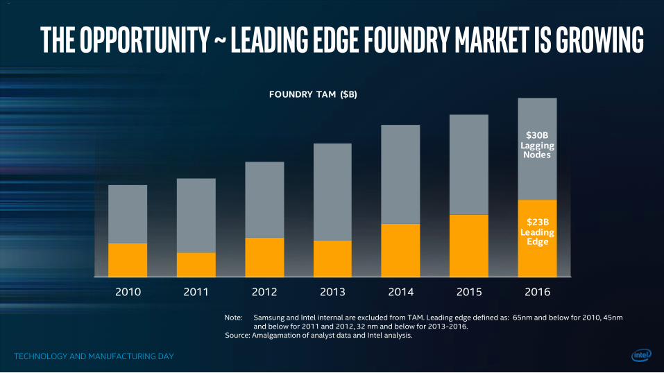
The opportunity ~ Leading edge foundry market is Growing57_84
Note: Samsung and Intel internal are excluded from TAM. Leading edge defined as: 65nm and below for 2010, 45nm and below for 2011 and 2012, 32 nm and below for 2013-2016.
Source: Amalgamation of analyst data and Intel analysis.
FOUNDRY TAM ($B)
2010 2011 2012 2013 2014 2015 2016
$23BLeading
Edge
$30BLaggingNodes
TECHNOLOGY AND MANUFACTURING DAY
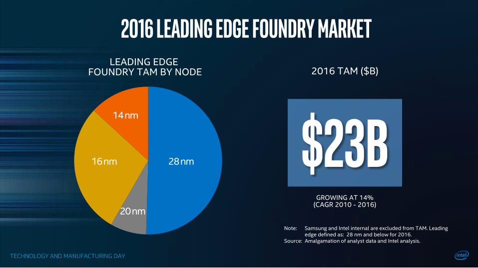
2016 Leading Edge Foundry MarketLEADING EDGE
FOUNDRY TAM BY NODE
$23BGROWING AT 14%
(CAGR 2010 - 2016)
2016 TAM ($B)
Note: Samsung and Intel internal are excluded from TAM. Leading edge defined as: 28 nm and below for 2016.
Source: Amalgamation of analyst data and Intel analysis.
TECHNOLOGY AND MANUFACTURING DAY
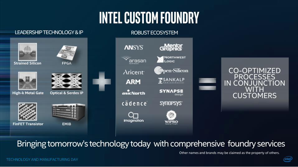
Intel Custom Foundry
Bringing tomorrow’s technology today with comprehensive foundry services
LEADERSHIP TECHNOLOGY & IP ROBUST ECOSYSTEM
High-k Metal Gate
Strained Silicon
FinFET Transistor
FPGA
Optical & Serdes IP
EMIB
CO-OPTIMIZED PROCESSES
IN CONJUNCTION WITH
CUSTOMERS
Other names and brands may be claimed as the property of others.

TECHNOLOGY AND MANUFACTURING DAY
Intel Custom Foundry ~ Enabling FINFET Capabilities
2nd gen FinFET technology in mass production targeting networking, FPGA and mobile SOC markets14 nm
10 nm3rd gen FinFET technology, targeting high performance client and mobile markets
Proven Capability: Intel has manufactured ~7M FinFET wafers
1st gen FinFET technology focused on the networking market22 nm GP

TECHNOLOGY AND MANUFACTURING DAY
Introducing 22FFL Platform
Cost Effective Design
Extreme Integration Capability
Ideal for highly integrated, cost sensitive products requiring a combination of high performance and ultra low power
22FFL
Fast Time to Market
Wearable DevicesAutomotive Smartphones
FinFET for the masses

TECHNOLOGY AND MANUFACTURING DAY
Putting It All TogetherWe continue to advance Moore’s Law
resulting in significant product and cost benefits
Our scale is a unique competitive advantage
We are building a foundry franchise
We continue to outpace the rest of the industry(~3 year lead on 14nm)
Source: Intel estimates

TECHNOLOGY AND MANUFACTURING DAY
One More Thing...
TECHNOLOGY AND MANUFACTURING DAY
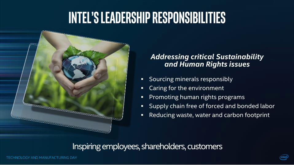
Intel’s Leadership Responsibilities
Inspiring employees, shareholders, customers
Addressing critical Sustainability and Human Rights issues
Sourcing minerals responsibly
Caring for the environment
Promoting human rights programs
Supply chain free of forced and bonded labor
Reducing waste, water and carbon footprint