Techniki nanoszenia Lecture 9 - Zespół Fizyki i...
44
L L Techniki nanoszenia Techniki nanoszenia Lecture Lecture 9 9
Transcript of Techniki nanoszenia Lecture 9 - Zespół Fizyki i...

L
LTechniki nanoszeniaTechniki nanoszenia
Lecture Lecture 99

Nano-Scale Sputter Deposition of Thin Films and Film Stacks for Data Storage Applications
W. Maass, B. Ocker, J. Langer
Ultrasmooth Workshop – Kraków, July 4-6, 2007

What are we talking about ?
OutlineThe challenge: Industrial deposition of thin films and film stacks for magnetic and magneto – electronic applications
General deposition concepts
Sputter deposition (PVD) technologies
Linear Dynamic Deposition – a successful PVD technology
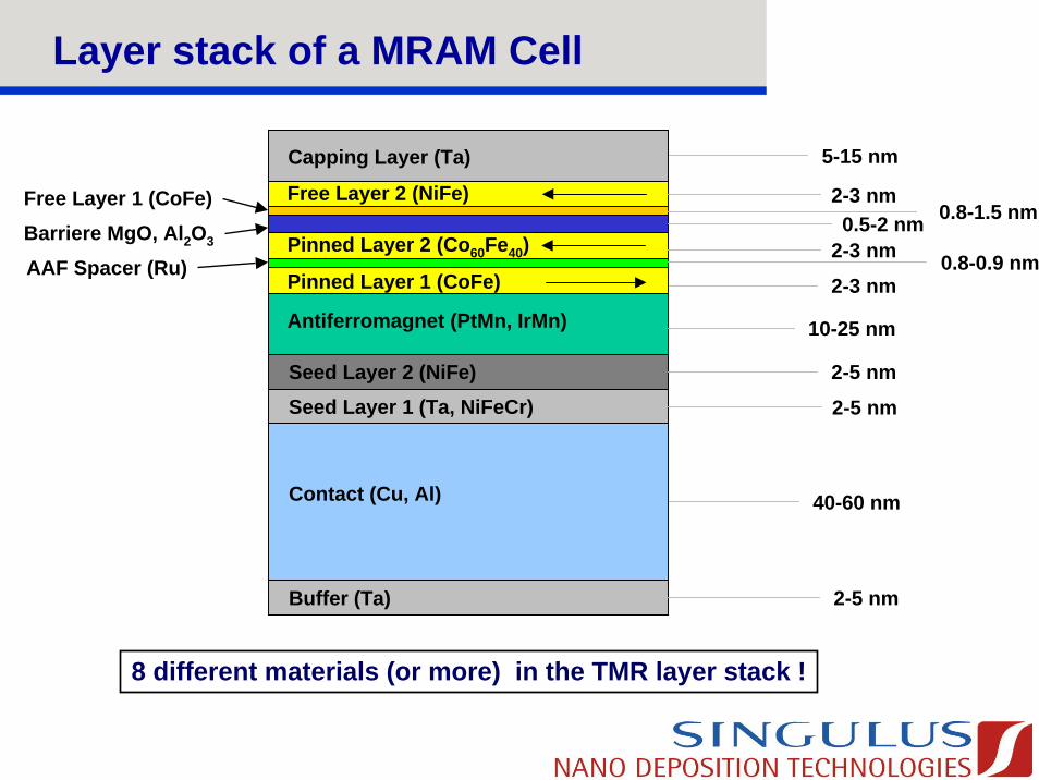
Layer stack of a MRAM Cell
Pinned Layer 1 (CoFe)
Pinned Layer 2 (Co60Fe40)
Free Layer 2 (NiFe)
Capping Layer (Ta)
Antiferromagnet (PtMn, IrMn)
Seed Layer 2 (NiFe)
Contact (Cu, Al)
Buffer (Ta)
Seed Layer 1 (Ta, NiFeCr)
Free Layer 1 (CoFe)
AAF Spacer (Ru)Barriere MgO, Al2O3
2-5 nm
40-60 nm
2-5 nm
2-5 nm
10-25 nm
0.8-1.5 nm0.5-2 nm
2-3 nm
2-3 nm
2-3 nm 0.8-0.9 nm
5-15 nm
8 different materials (or more) in the TMR layer stack !

Layer stack of a MRAM Cell
Pinned Layer 1 (CoFe)
Pinned Layer 2 (Co60Fe40)
Free Layer 2 (NiFe)
Capping Layer (Ta)
Antiferromagnet (PtMn, IrMn)
Seed Layer 2 (NiFe)
Contact (Cu, Al)
Buffer (Ta)
Seed Layer 1 (Ta, NiFeCr)
Free Layer 1 (CoFe)Barriere MgO, Al2O3
AAF Spacer (Ru)
2-5 nm
40-60 nm
2-5 nm
2-5 nm
10-25 nm
0.8-1.5 nm0.5-2 nm
2-3 nm
2-3 nm
2-3 nm 0.8-0.9 nm
5-15 nm
8 different materials (or more) in the TMR layer stack !
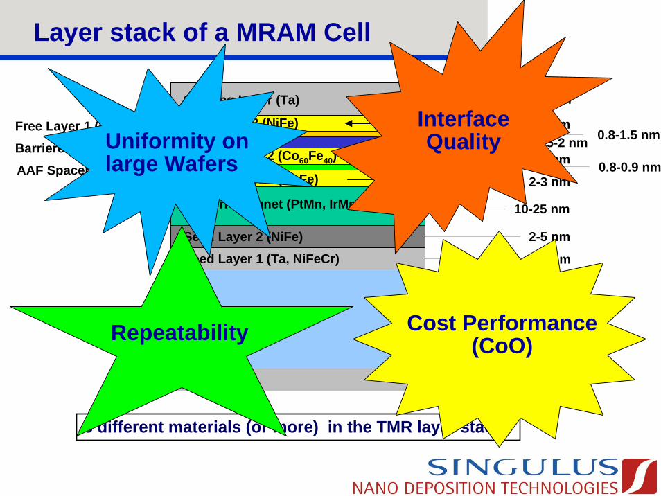
Uniformity on large Wafers

Layer stack of a MRAM Cell
Pinned Layer 1 (CoFe)
Pinned Layer 2 (Co60Fe40)
Free Layer 2 (NiFe)
Capping Layer (Ta)
Antiferromagnet (PtMn, IrMn)
Seed Layer 2 (NiFe)
Contact (Cu, Al)
Buffer (Ta)
Seed Layer 1 (Ta, NiFeCr)
Free Layer 1 (CoFe)Barriere MgO, Al2O3
AAF Spacer (Ru)
2-5 nm
40-60 nm
2-5 nm
2-5 nm
10-25 nm
0.8-1.5 nm0.5-2 nm
2-3 nm
2-3 nm
2-3 nm 0.8-0.9 nm
5-15 nm
8 different materials (or more) in the TMR layer stack !
Uniformity on large Wafers
Interface Quality
Repeatability
Layer stack of a MRAM Cell
Pinned Layer 1 (CoFe)
Pinned Layer 2 (Co60Fe40)
Free Layer 2 (NiFe)
Capping Layer (Ta)
Antiferromagnet (PtMn, IrMn)
Seed Layer 2 (NiFe)
Contact (Cu, Al)
Buffer (Ta)
Seed Layer 1 (Ta, NiFeCr)
Free Layer 1 (CoFe)Barriere MgO, Al2O3
AAF Spacer (Ru)
2-5 nm
40-60 nm
2-5 nm
2-5 nm
10-25 nm
0.8-1.5 nm0.5-2 nm
2-3 nm
2-3 nm
2-3 nm 0.8-0.9 nm
5-15 nm
8 different materials (or more) in the TMR layer stack !
Uniformity on large Wafers
Interface Quality
Repeatability Cost Performance (CoO)
…. and more…. and more…. and more

Non – AFC Multilayer for TFH
NiFe 1.5/7x[ FeCo30 25/Al2O3 0.5/NiFe 1.0]/FeCo30 25/NiCr 3 200nm FeCo(5% N2 during FeCo deposition)
Cap
CoFe 25
CoFe 25
Seed
High magnetic Moment Bs
Interface quality
Hce, Hch, Hk, Br
Uniformity on large wafers
Repeatability
Cost of OwnershipAl2O3NiFe
Magnetic EA alignment

Vacuum deposition technologies
What do we use?
Evaporation
CVD (Chemical Vapor Deposition)
ALD (Atomic Layer deposition)
IBD (Ion Beam Deposition)
PVD (Physical Vapor Deposition)

Vacuum deposition technologies: PVD
Target = Cathode
Substrate AnodeAnode
Ar (Kr) Ions
Electrons
DC, RFPlasma Plasma
Ar (Kr) of low pressure ( < 10-2 mbar)
Permanent Magnets Magnetron
S N S Cooling
S N
Aligning Magnetic Field (AMF)

Vacuum deposition technologies: PVD
Static Deposition by circular cathodePermanent Magnets (cross section: )
Pro’s:• Efficient deposition• Simple technology
Con’s:• Poor thickness uniformity• Not good for very thin films (1 – 2 nm)• Not useable for ferromagnetic films
Leakage field
Target
Substrate
Distance
S N S

Vacuum deposition technologies: PVD
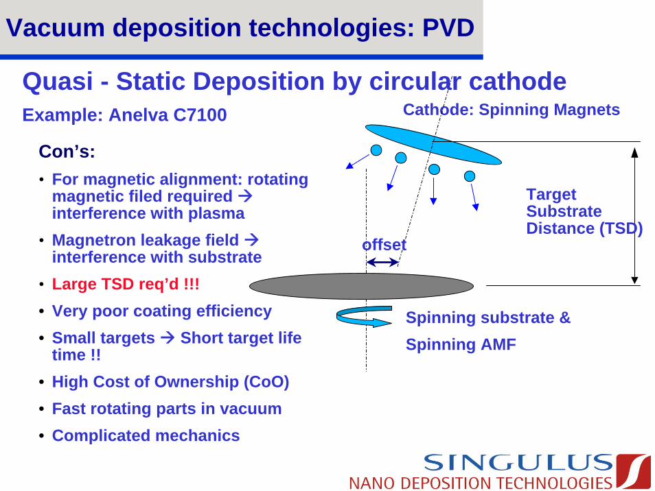
Quasi - Static Deposition by circular cathodeExample: Anelva C7100
Pro’s:• Small targets (pro for R&D)• Co-Sputter feasible
Features:Uniformity by (fast) substrate rotationCathode – substrate material flow with angle of incidence and offsetSpinning magnetron magnets for target utilizationC7100: 4, 5 or 8 (small) cathodes / chamber; up to four chambers / tool, base pressure 5*10-9 mbarC7100: up to 200mm waferC7100EX: up to 300mm wafer
Cathode: Spinning Magnets
Spinning substrate &Spinning AMF
Target Substrate Distance (TSD)
offset
Vacuum deposition technologies: PVD
Con’s:• For magnetic alignment: rotating
magnetic filed required interference with plasma
• Magnetron leakage field interference with substrate
• Large TSD req’d !!!• Very poor coating efficiency• Small targets Short target life
time !!• High Cost of Ownership (CoO)• Fast rotating parts in vacuum• Complicated mechanics
Cathode: Spinning Magnets
Spinning substrate &Spinning AMF
Target Substrate Distance (TSD)
offset
Quasi - Static Deposition by circular cathodeExample: Anelva C7100

Vacuum deposition technologies: PVD
Dynamic DepositionExample: Leybold, BPS, Unaxis Corona; Emerald I, II; Cyberite PVD
Pro’s:• Simple cathode design• Proven technology• Batch load good for throughput
Con’s:• Poor uniformity, but “Aperture shaper”• Bad coating efficiency CoO?• For magnetic alignment magnetic
field moving with wafer required TSD !!
• Magnetron leakage field interference with substrate TSD!!
Target = Cathode
Turn - table
Substrate
Features:Batch load possibleCorona/Emerald I: 4 cathodes,
max. 150mm wafer, 1*10-7 mbarEmerald II: 6 cathodes,
max. 200mm wafer, 1*10-7 mbarCyberite PVD: 10 cathodes, no
batch load possiblemax. 200mm wafer, 1*10-8 mbar

Vacuum deposition technologies: PVD
Dynamic Deposition VariantsExample: Veeco Nexus, PVD-10P
Pro’s:• Simple cathode design
Con’s:• Uniformity by rotating & moving
substrate• For magnetic alignment: rotating &
moving magnetic filed required interference with plasma TSD !!
• Magnetron leakage field interference with substrate TSD!!
• CoO ??• Complicated mechanics, fast rotating
parts in vacuum
Target = Cathode
Turn - table
Substrate
Features:10 cathodes (PVD-10) or 12 cathodes (Nexus)Tools for up to 200mm wafer Base pressure: 5*10-9 mbar

Deposition Area
Wafer Travel
Static DepRate
Magnet Array
Sputter Target
Wafer
Pro’s:•Leakage field of cathode parallel to wafer travel direction:
- Ideal symmetry for magnetic film applications
•Stationary Aligning Magnetic Field (AMF):
- AMF can be optimized with cathode
Linear Dynamic Deposition (LDD)Example: Singulus TIMARIS
Vacuum deposition technologies: PVD
SN
Yoke Yoke

Deposition Area
Wafer Travel
Static DepRate
Magnet Array
Sputter Target
Wafer
Pro’s:•Short Target-Substrate Distance:
- Good Coating Efficiency•Thickness adjusted by wafer speed:
- Tight control & repeatability•No fast moving parts in vacuum
- Robust and reliable design
Vacuum deposition technologies: PVD
Linear Dynamic Deposition (LDD)Example: Singulus TIMARIS

Magnet Array
Sputter Target
Wafer
Features TIMARIS:Thickness (and other materials) uniformity obtained by cathode – substrate geometry
10 targets in one PVD chamber, max. two 10-PVD chambers / tool high throughput
Other modules: Oxi, Soft-Etch
Bridge tool: Wafer diameter 150mm, 200mm, 300mm
Ultra – High – Vacuum design(5*10-9 mbar base pressure)
Robust and reliable mechanics
Vacuum deposition technologies: PVD
Linear Dynamic Deposition (LDD)Example: Singulus TIMARIS
Target Drum Targets

A Proven Deposition Tool for TFH, MRAM and other Semiconductor Applications
300/200/150/100mm PVD Bridge System
TIMARIS: 20 years of Experience
In its history the NDT team has designed, built and run different types of production tools (PVD, IBD, CVD) forThin Film Head Manufactering (e.g. Ferro – Magnetic films and film stacks)Flat Panel Display (large area deposition)Semiconductor (e.g. Metallization)
TIMARIS

Business Summary SINGULUS Nano Deposition Technologies
Business Unit:Core Team now 27 people + approx. 10 to 15 additional workers (Singulus operations and non –permanent)
Clean Room:
• 40 sqm class 1.000 (R&D)
• 160 sqm class 10.000 (Assembly)
Key Metrology:
• CIPT – TMR Metrology (CAPRES)
• MOKE
• VSM
• KLA – Tencor TBI
• AFM
• 4PP Sheet Resistance Mapper (Ø300mm)
• Spectral Ellipsometer
New R&D Tool with RF capability under installation in Singulus Clean Room
Installed Base until Q2/07One system shipped to customer in Q4/06 for Thin Film Head production
Two more systems shipped in Q1/07 for MRAM production (1xUS, 1xEU)
One additional system for Thin Film Head production just shipped to the customer
Order Backlog as of Q2/07One system for TFH production, to be shipped to customer by Q1/08
TIMARIS for MRAM, Magnetic Read/Write head production and other Semiconductor applications
PVD Bridge system: 300mm (12”), 200mm (8”) and 150mm (6”) capability

TIMARIS: Production area (clean rooms)

TIMARIS: Photography
Multi Target ModuleTop: Target Drum with 10 rectangular cathodes; Drum design ensures easy maintenance;Bottom: Main part of the chamber containing LDD equipment
Transport Module(UHV wafer handler)
Oxidation ModuleLow Energy Remote Atomic Plasma Oxidation;Natural Oxidation;Soft Energy Surface Treatment
Soft-Etch Module(PreClean, Surface Treatment)
Cassette Module(according to Customer request)
Ultra – High – Vacuum Design: Base Pressure ≤ 5*10-9 Torr (Deposition Chamber)High Throughput (e.g. MRAM): 9 Wafer/Hour (1 Depo-Module), 18 Wafer/Hour (2 Depo-Module)High Effective Up-time: Maintenance friendly DesignReliability: Solid and well Engineered Design, no fast moving Parts

TIMARIS: Layout including cabinets
Typical Cluster Tool Configuration for 150 mm or 200mm wafer processing:(TFH production, MRAM pilot production, R&D)
Oxi-Module
(27.8 ft)
(15.
7 ft)
Configuration can be modified according to customer request.
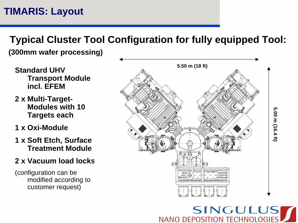
Typical Cluster Tool Configuration for fully equipped Tool:(300mm wafer processing)
Standard UHV Transport Module incl. EFEM
2 x Multi-Target-Modules with 10 Targets each
1 x Oxi-Module1 x Soft Etch, Surface
Treatment Module2 x Vacuum load locks(configuration can be
modified according to customer request)
TIMARIS: Layout5.00 m
(16.4 ft)
5.50 m (18 ft)

TIMARIS: Thickness Uniformity
@ 200 mm, 6mm edge exclusionAl 0.16% (1σ)Cu 0.42% (1σ)NiFe 0.36% (1σ)CoFe 0.22% (1σ)Ta 0.41% (1σ)PtMn 0.24% (1σ) Ru 0.17% (1σ)IrMn 0.18% (1σ)NiFeCr 0.24% (1σ)
Al 0.23% (1σ)Cu 0.43% (1σ)NiFe 0.66% (1σ)CoFe40 0.77% (1σ)Ta 0.51% (1σ)PtMn 0.34% (1σ)Ru 0.50% (1σ)IrMn 0.59% (1σ)NiFeCr 0.80% (1σ)
@ 300 mm, 6mm edge exclusion300 mm data
200 mm data

As deposited GMR stack (no pinning):Ta10/PtMn20/CoFe2/Ru(x)/CoFe2/Cu2.2/CoFe0.8/NiFe3.8/Ta5 (thickness in nm)
TIMARIS: Thickness Control, Example GMR
Effect of AF coupling in the AAF structure:CoFe2/Ru(x)/CoFe2

50
100
150
200
250
50 100 150 200 250
X - position [mm]
Y - p
ositi
on [m
m
Non – AFC Multilayer using Fe70Co30 :
TIMARIS: CoFe Multilayer
NiFe 1.5/7x[ FeCo30 25/Al2O3 1.0/NiFe 1.0]/FeCo30 25/NiCr 3 200nm FeCo(5% N2 during FeCo deposition)
Hce: 3.0 OeHk: 99.2 OeHch: 3.8 OeMr/Ms: 4.0 %
Cap
CoFe 25
CoFe 25
Seed
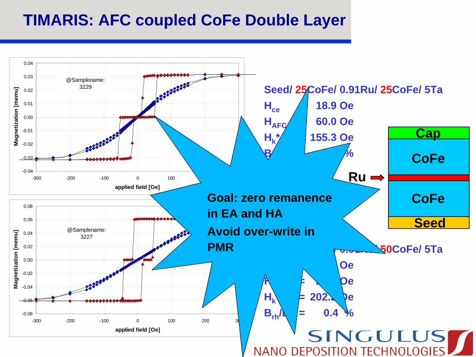
Seed/ 25CoFe/ 0.91Ru/ 25CoFe/ 5TaHce = 18.9 OeHAFC = 60.0 OeHk* = 155.3 OeBrh/Bs = 1.2 %
TIMARIS: AFC coupled CoFe Double Layer
-0.04
-0.03
-0.02
-0.01
0.00
0.01
0.02
0.03
0.04
-300 -200 -100 0 100 200 300
applied field [Oe]
Mag
netiz
atio
n [m
emu]
@Samplename: 3229
Seed/ 50CoFe/ 0.91Ru/ 50CoFe/ 5TaHce = 31.2 OeHAFC = 27.3 OeHk* = 202.2 OeBrh/Bs = 0.4 %-0.08
-0.06
-0.04
-0.02
0.00
0.02
0.04
0.06
0.08
-300 -200 -100 0 100 200 300
applied field [Oe]
Mag
netiz
atio
n [m
emu] @Samplename:
3227
CoFe
Seed
CoFeRu
Cap
Goal: zero remanence in EA and HAAvoid over-write in PMR

TIMARIS: Al2O3 - TMR vs. RA - Summary

TIMARIS: MgO – TMR - Summary
MgO – Barrier, TMR vs. RA:

TIMARIS: MgO – TMR, Summary
RF sputtered MgO – Barrier: TMR & RA vs. MgO Thickness:(Comparison of different Target Vendors)

TIMARIS: Remote Plasma Oxidation uniformity
Improvement by grid optimization
Steps:• Reduction of grid transparency (oxidation at higher power)• Grid optimization using sheet resistance of Ta/Al-ox layers• Final grid optimization using RA uniformity across wafer

Measured by CIPT
TIMARIS: Oxidation Uniformity (Al2O3 – Barrier)

TIMARIS: Repeatability (Al2O3 – Barrier)
Measured by MOKE

-100 -50 0 50 100
-100
-50
0
50
100
X Axis Title
Y A
xis
Title
49,70
49,86
50,02
50,18
50,34
50,50
50,66
50,82
50,98
51,14
51,30
Mg concentration in MgO: 50.48at%, 1σ = 0.45at%
XRF - etch / Ta 10 / PtMn64 0.5kW 150sccm 15 / CoFe20 2.4 / Ru 0.7 / CoFeB 2.8 / Mg 1.2 / ox 250W 10s 90sccm/ CoFeB 3.2 / Ta 10
-100 -50 0 50 100
-100
-50
0
50
100
X Axis Title
Y A
xis
Title
1,190E4
1,194E4
1,197E4
1,201E4
1,205E4
1,209E4
1,212E4
1,216E4
1,220E4
1,223E4
1,227E4
Mg content and MgO thickness in plasma-oxidized Mg MTJ measured by XRF
MgO - thickness: 1.21nm, 1σ = 0.71%
TIMARIS: MgO TMR Uniformity
Mg Sputtering + Oxidation
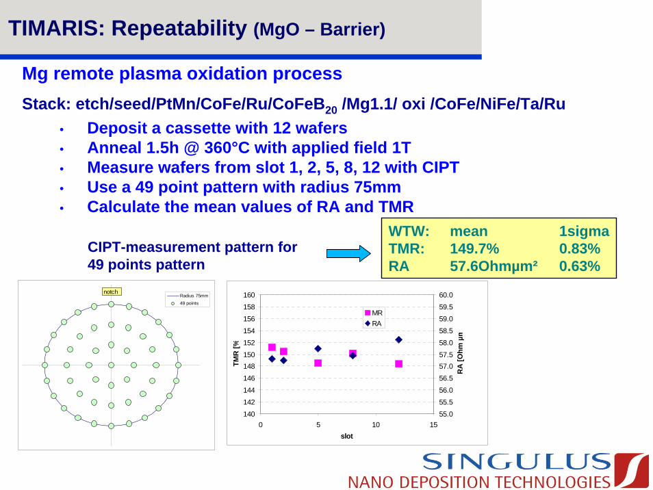
• Deposit a cassette with 12 wafers • Anneal 1.5h @ 360°C with applied field 1T • Measure wafers from slot 1, 2, 5, 8, 12 with CIPT• Use a 49 point pattern with radius 75mm• Calculate the mean values of RA and TMR
Stack: etch/seed/PtMn/CoFe/Ru/CoFeB20 /Mg1.1/ oxi /CoFe/NiFe/Ta/Ru
CIPT-measurement pattern for 49 points pattern
WTW: mean 1sigmaTMR: 149.7% 0.83%RA 57.6Ohmµm² 0.63%
Radius 75mm49 points
notch
140142144146148150152154156158160
0 5 10 15slot
TMR
[%
55.055.556.056.557.057.558.058.559.059.560.0
RA
[Ohm
µm
MRRA
TIMARIS: Repeatability (MgO – Barrier)
Mg remote plasma oxidation process

Stack: etch /buffer/PtMn/CoFe/Ru/CoFeB20/Mg/ natural oxidation /CoFe/NiFe/Ta/CuN/Ru
Mg natural oxidation process 1*10-7 mbar
TMRMean: 119.5%1sigma: 5.0%
RAMean: 9.52Ohmµm²1sigma: 3.7%
-80000 -60000 -40000 -20000 0 20000 40000 60000 80000-80000
-60000
-40000
-20000
0
20000
40000
60000
80000
X Axis Title
Y Ax
is T
itle
106.7
109.4
112.0
114.7
117.3
120.0
122.7
125.3
128.0
TMRnotch
-80000 -60000 -40000 -20000 0 20000 40000 60000 80000-80000
-60000
-40000
-20000
0
20000
40000
60000
80000
X Axis Title
Y A
xis
Title
8.970
9.134
9.299
9.463
9.627
9.792
9.956
10.12
10.29
RAnotch
Uniformity by49-point pattern
TIMARIS: MgO – TMR, Summary

Breakdown Voltage for different MgO preparation techniques(0.1 x 0.2 µm² devices)
TIMARIS: MgO – TMR, Summary

Current Induced Switching or Spin-Torque-Transfer Switching
TIMARIS: Next generation MRAM : CIS
Results obtained in cooperation with Grandis Inc., see e.g.Zhitao Diao et al., Applied Physics Letters 87, 232502 (2005)
Stack (c, d) : Ta5/PtMn30/CoFe3/Ru0.8/CoFeB2/AlOx /CoFeB2.5/Ta5 (nm)TMR ≈ 25%, RA ≈ 15 Ω*µm²ic ≈ 4.3*106 A/cm²
Stack (a,b) : Ta5/PtMn20/CoFe2/Ru0.8/CoFeB2/MgO/CoFeB2.5/Ta8 (nm)TMR ≈ 150%, RA ≈ 50 Ω*µm²ic ≈ 1.1*106 A/cm²

Current Induced Switching or Spin-Torque-Transfer Switching
TIMARIS: Next generation MRAM : CIS
Lowest Jc0 measured(Grandis – Timaris)

TIMARIS: Unique Selling Points
TMR Wafer Production (MRAM and Thin Film Head)High Throughput (incl. load and pre – clean):
- Stack: Generic MRAM TMR: ≈ 9 wafer/h (1 MTM), ≈ 18 wafer/h (2 MTM)- Stack: Generic Low RA (MgO) TMR: ≈ 5 wafer/h (1 OM), ≈ 8 wafer/h (2
OM)High Yield/Wafer by uniform TMR & Magnetic PropertiesTight Thickness Control of Ultra-Thin Films
- Thinnest Film < 0.1 nm; Smallest Thickness Step: < 0.01 nmFull flexibility regarding PVD – mode for all targets: DC, pulsed DC, RFLonger production Cycles:
- Approx. 6500 TMR wafers until target replacement & strip/clean ( approx. 4 weeks production 24h/7d)
Costs/Wafer: - 6 – 7 US$/wafer (20nm PtMn deposition assumed)- Will save up to 1.0 Mio US$ compared with other TMR PVD tools
(18 wafer/h, 24h/7d production assumed)