TECHNICAL UNIVERSITY OF CRETE ELECTRICAL AND …
131
Transcript of TECHNICAL UNIVERSITY OF CRETE ELECTRICAL AND …

TECHNICAL UNIVERSITY OF CRETE
ELECTRICAL AND COMPUTER ENGINEERING DEPARTMENT
Design of low power operational transconductance ampliers(OTAs) in two generations of Bulk CMOS
by
Apostolos Apostolakis
A THESIS SUBMITTED IN PARTIAL FULFILLMENT OF THE REQUIREMENTS FOR THEDIPLOMA DEGREE OF ELECTRICAL AND COMPUTER ENGINEERING
THESIS COMMITTEE
Associate Professor Matthias Bucher, Supervisor
Professor Costas Balas
Professor Konstantinos Kalaitzakis

To the memory of my grandmother Maria and my uncle George
Chania, December 2019

Acknowledgements
First of all, I would like to thank my supervisor, Prof. Matthias Bucher, for his guidance and advicethroughout this work as well as for the opportunity to work on an innovative technology eld.
Moreover, I would like to thank Prof. Costas Balas and Prof. Konstantinos Kalaitzakis becausethey have accepted to be my thesis committee. I also oer my sincere appreciation for the learningopportunities provided by them in the eld of electronics during my studies.
Furthermore, I would like to thank all the members of the microelectronics group of the Electronicslaboratory of Technical University of Crete. Although their very busy schedule, they have always beenavailable for me to solve the questions that I had. More specically, I would like to thank AlexiaPapadopoulou who has given me incredible help during the entire procedure of this thesis. This thesiswould not be possible without her help and patience.
Finally, I must express my very profound gratitude to my parents, my sister, my friends and mygirlfriend for providing me with unfailing support and continuous encouragement throughout my yearsof study and through the process of researching and writing this thesis. This accomplishment wouldnot have been possible without them.
i

Abstract
The continued need for accurate design methodologies mandates an ongoing research in this eld.In this work, the Inversion Coecient (IC) based methodology for low-power, low-voltage MOSFETdesign was explored. This methodology is based on design-oriented transistor parameter extraction,such as I0 (technology current), slope factor n, transconductance parameter KP etc. and severalimportant performance metrics in the form of Figures-of-Merit (FoM), such as gm/ID and AV (intrinsicgain). To test the accuracy of this approach, two dierent operational transconductance amplier(OTA) topologies were designed in low power mode of operation (power dissipation 24uW ), a currentmirror p-input, single-ended OTA and a p-input, fully dierential, folded cascode (FDFC) OTA. Toaccentuate the prediction capability of this methodology, two process design kits (PDKs) were used;a 65nm bulk CMOS PDK and a 90nm bulk CMOS PDK. The structural design ow includes theprocedure of parameter extraction for both PDKs, the mathematical analysis of each circuit, thedesign validation and optimization via simulation. All four designs were developed in Virtuoso ADEby Cadence and simulated using Spectre Simulation Platform. Open-Loop Gain (A0), Gain Bandwidth(GBW ), Phase Margin (PM), Slew Rate (SR), Input and Output Voltage ranges, Input referred Noiseand Input DC oset were set as circuit performance criteria. Finally, comparative results betweencircuit topologies and technology nodes are presented and discussed.
Περίληψη
Η διαρκής ανάγκη για ακριβείς μεθοδολογίες σvχεδίασvης απαιτεί μια σvυνεχή έρευνα σvτον τομέα αυτό. Σεαυτή την εργασvία, διερευνήθηκε η μεθοδολογία που βασvίζεται σvτον δείκτη ανασvτροφής (IC) για σvχεδιασvμόκυκλωμάτων μεMOSFET, χαμηλής ισvχύος και χαμηλής τάσvης. Αυτή η μεθοδολογία βασvίζεται σvτην εξαγ-ωγή παραμέτρων των τρανσvίσvτορ προσvανατολισvμένη σvτη σvχεδίασvη, όπως το I0 (ρεύματος τεχνολογίας),τον σvυντελεσvτής κλίσvης n, την παράμετρο διαγωμιμότητας KP κλπ. και αρκετές σvημαντικές μετρικέςαπόδοσvης (FoM), όπως gm/ID and AV (ενδογενές κέρδος). Για να εξετασvτεί η ακρίβεια αυτής τηςπροσvέγγισvης, σvχεδιάσvτηκαν δύο διαφορετικές τοπολογίες τελεσvτικών ενισvχυτών διαγωγιμότητας (OTA)σvε λειτουργία χαμηλής ισvχύος (απόδοσvη ισvχύος 24uW ), έναν p-εισvόδου καθρέφτη ρεύματος τελεσvτικόενισvχυτή διαγωγιμότητας OTA μονής εξόδου και έναν τελεσvτικό ενισvχυτή διαφορικής εξόδου (FDFC)ΟΤΑ. Για να τονισvθεί η δυνατότητα πρόβλεψης της σvυγκεκριμένης μεθοδολογίας, χρησvιμοποιήθηκανδύο διαφορετικά κιτ σvχεδιασvμού (PDKs)· ένα CMOS PDK 65nm και ένα CMOS PDK 90nm. Η δι-αδικασvία δομικής σvχεδίασvης περιλαμβάνει την εξαγωγή παραμέτρων και για τα δύο PDK, τη μαθηματικήανάλυσvη κάθε κυκλώματος, την επαλήθευσvη των αποτελεσvμάτων της σvχεδίασvης και τη βελτισvτοποίησvημέσvω προσvομοίωσvης. Και οι τέσvσvερις σvχεδιάσvεις αναπτύχθηκαν σvτο Virtuoso ADE από την Cadenceκαι προσvομοιώθηκαν με τη χρήσvη του Spectre Simulation Platform. Το κέρδος ανοικτού βρόχου (A0),το εύρος ζώνης κέρδους (GBW ), το περιθώριο φάσvης (PM), ο ρυθμός μετατόπισvης (SR), τα εύρητάσvης εισvόδου και εξόδου, καθορίσvτηκαν ως κριτήρια απόδοσvης κυκλώματος. Τέλος, παρουσvιάζονται καιαναλύονται σvυγκριτικά αποτελέσvματα μεταξύ των τοπολογιών και των διαφορετικών τεχνολογιών.
ii

Contents
1 Introduction 11.1 Technology Parameters extraction and OTAs design and implementation . . . . . . . . . 11.2 Thesis structure . . . . . . . . . . . . . . . . . . . . . . . . . . . . . . . . . . . . . . . . . 1
2 Basic MOSFET device physics and structure 22.1 Structure of a MOSFET transistor . . . . . . . . . . . . . . . . . . . . . . . . . . . . . . 32.2 Basic description of MOSFET operation . . . . . . . . . . . . . . . . . . . . . . . . . . . 5
2.2.1 Creating a channel for current conduction . . . . . . . . . . . . . . . . . . . . . . 52.2.2 Applying VDS voltage . . . . . . . . . . . . . . . . . . . . . . . . . . . . . . . . . 7
2.3 Inversions regions & Inversion Coecient (IC) . . . . . . . . . . . . . . . . . . . . . . . . 7
3 Technology parameters extraction 93.1 Simulated transfer and output IDS − VGS , IDS − VDS characteristics . . . . . . . . . . 93.2 Oxide capacitance Cox extraction . . . . . . . . . . . . . . . . . . . . . . . . . . . . . . . 12
3.2.1 MOSFET dependency of gate-source voltage VGS . . . . . . . . . . . . . . . . . . 123.2.2 MOSFET parasitic capacitances . . . . . . . . . . . . . . . . . . . . . . . . . . . 143.2.3 The MOS capacitor . . . . . . . . . . . . . . . . . . . . . . . . . . . . . . . . . . 143.2.4 MOSFET Oxide-related capacitances and COX extraction methodology . . . . . 153.2.5 Simulation and results . . . . . . . . . . . . . . . . . . . . . . . . . . . . . . . . . 16
3.3 Slope factor n and technology current I0 extraction . . . . . . . . . . . . . . . . . . . . . 173.3.1 Slope factor n denition . . . . . . . . . . . . . . . . . . . . . . . . . . . . . . . . 173.3.2 Technology current I0 denition . . . . . . . . . . . . . . . . . . . . . . . . . . . 173.3.3 Slope factor n and technology current I0 extraction methodology . . . . . . . . . 183.3.4 Simulation and results . . . . . . . . . . . . . . . . . . . . . . . . . . . . . . . . . 19
3.4 Carrier mobility µ and transconductance parameter Kp . . . . . . . . . . . . . . . . . . 193.4.1 Carrier mobility µ denition . . . . . . . . . . . . . . . . . . . . . . . . . . . . . . 193.4.2 Transconductance parameter Kp denition . . . . . . . . . . . . . . . . . . . . . 203.4.3 Transconductance parameter Kp and carrier mobility µ extraction methodology . 203.4.4 Simulation and results . . . . . . . . . . . . . . . . . . . . . . . . . . . . . . . . . 21
3.5 Transconductance eciency gmID
and transit frequency fT extraction . . . . . . . . . . . 213.5.1 MOS Transconductance gm denition . . . . . . . . . . . . . . . . . . . . . . . . 213.5.2 Transit frequency fT denition . . . . . . . . . . . . . . . . . . . . . . . . . . . . 223.5.3 Transconductance eciency gm
IDextraction as a Figure of Merit (FoM) . . . . . . 23
3.5.4 Transconductance eciency multiplied by transit frequency gmfTID
extraction asa Figure of Merit (FoM) . . . . . . . . . . . . . . . . . . . . . . . . . . . . . . . . 23
3.5.5 Simulation and results . . . . . . . . . . . . . . . . . . . . . . . . . . . . . . . . . 243.6 Early Voltage Ua extraction . . . . . . . . . . . . . . . . . . . . . . . . . . . . . . . . . . 26
3.6.1 Output conductance gds in saturation and early voltage denitions . . . . . . . . 263.6.2 Early voltage Ua extraction methodology . . . . . . . . . . . . . . . . . . . . . . 263.6.3 Simulation and results . . . . . . . . . . . . . . . . . . . . . . . . . . . . . . . . . 27
3.7 Intrinsic gain AV extraction . . . . . . . . . . . . . . . . . . . . . . . . . . . . . . . . . . 283.7.1 Intrinsic gain AV denition and extraction methodology . . . . . . . . . . . . . . 283.7.2 Simulation and results . . . . . . . . . . . . . . . . . . . . . . . . . . . . . . . . . 28
3.8 Flicker or 1/f noise extraction . . . . . . . . . . . . . . . . . . . . . . . . . . . . . . . . 293.8.1 Noise in MOSFETs . . . . . . . . . . . . . . . . . . . . . . . . . . . . . . . . . . . 293.8.2 Flicker or 1/f noise denition and extraction methodology . . . . . . . . . . . . 293.8.3 Simulation and results . . . . . . . . . . . . . . . . . . . . . . . . . . . . . . . . . 31
3.9 Current and voltage MOSFET mismatch σ( δIDID ), σ(δVG) extraction . . . . . . . . . . . 323.9.1 Mismatch denition . . . . . . . . . . . . . . . . . . . . . . . . . . . . . . . . . . 323.9.2 Current and voltage MOSFET mismatch σ( δIDID ), σ(δVG) denition and extrac-
tion methodology . . . . . . . . . . . . . . . . . . . . . . . . . . . . . . . . . . . . 323.9.3 Simulation and results . . . . . . . . . . . . . . . . . . . . . . . . . . . . . . . . . 33
iii

3.10 Comparative results of the technology parameters . . . . . . . . . . . . . . . . . . . . . . 353.11 Cadence simulation schematics . . . . . . . . . . . . . . . . . . . . . . . . . . . . . . . . 36
4 Operational Transconductance Ampliers (OTAs) 404.1 Basic theoretical Analysis of OTAs . . . . . . . . . . . . . . . . . . . . . . . . . . . . . . 40
4.1.1 Basic analog structures . . . . . . . . . . . . . . . . . . . . . . . . . . . . . . . . 404.1.2 Circuit partitioning and behavioral model of an analog amplier . . . . . . . . . 424.1.3 Denitions of the basic design parameters . . . . . . . . . . . . . . . . . . . . . . 43
4.2 Simple OTA design . . . . . . . . . . . . . . . . . . . . . . . . . . . . . . . . . . . . . . . 494.2.1 Theoretical design and operation . . . . . . . . . . . . . . . . . . . . . . . . . . . 494.2.2 Specications and sizing . . . . . . . . . . . . . . . . . . . . . . . . . . . . . . . . 504.2.3 Results and Analysis . . . . . . . . . . . . . . . . . . . . . . . . . . . . . . . . . . 56
4.3 Fully Dierential Folded Cascode OTA (FDFC OTA) . . . . . . . . . . . . . . . . . . . 654.3.1 Theoretical Design and operation . . . . . . . . . . . . . . . . . . . . . . . . . . . 654.3.2 Specications and sizing . . . . . . . . . . . . . . . . . . . . . . . . . . . . . . . . 674.3.3 Results and Analysis . . . . . . . . . . . . . . . . . . . . . . . . . . . . . . . . . . 75
4.4 Comparative results of the technology parameters . . . . . . . . . . . . . . . . . . . . . . 894.5 Cadence simulation schematics . . . . . . . . . . . . . . . . . . . . . . . . . . . . . . . . 91
A Appendix 95A.1 Matlab codes . . . . . . . . . . . . . . . . . . . . . . . . . . . . . . . . . . . . . . . . . . 95
References 117
iv

List of Figures
2.1 Cross section of (a) an n-type MOSFET (Substrate connection is also depicted) (b)Zoomed Gate region. . . . . . . . . . . . . . . . . . . . . . . . . . . . . . . . . . . . . . . 3
2.2 Physical structure of the NMOS transistor: (a) perspective view (b) top view. . . . . . . 42.3 Cross section of a p-type MOSFET . . . . . . . . . . . . . . . . . . . . . . . . . . . . . 42.4 Cross-section of a CMOS integrated circuit. . . . . . . . . . . . . . . . . . . . . . . . . . 52.5 Circuit symbols: (a) NMOS (b) PMOS. . . . . . . . . . . . . . . . . . . . . . . . . . . . 52.6 NMOS transistor with zero voltage applied to the gate. . . . . . . . . . . . . . . . . . . 62.7 NMOS transistor with a positive voltage applied to the gate. An n channel is induced
at the top of the substrate beneath the gate. . . . . . . . . . . . . . . . . . . . . . . . . 62.8 Mosfet operation: (a) Linear region (b) Channel pinch-o, saturation. . . . . . . . . . . 73.1 Simulated transfer and output characteristics (W/L = 500nm/500nm) for (a), (c) n-
type and (b), (d) p-type MOSFETs of 90nm bulk CMOS process. . . . . . . . . . . . . . 103.2 Simulated IDS vs. VGS (parametric sweep for dierent VGS) and IDS vs. VDS (paramet-
ric sweep for dierent VDS) characteristics (W/L = 500nm/500nm) for (a), (c) n-typeand (b), (d) p-type MOSFETs of 90nm bulk CMOS process. . . . . . . . . . . . . . . . . 10
3.3 Simulated transfer and output characteristics (W/L = 500nm/500nm) for (a), (c) n-type and (b), (d) p-type MOSFETs of 65nm bulk CMOS process. . . . . . . . . . . . . . 11
3.4 Simulated IDS vs. VGS (parametric sweep for dierent VGS) and IDS vs. VDS (paramet-ric sweep for dierent VDS) characteristics (W/L = 500nm/500nm) for (a), (c) n-typeand (b), (d) p-type MOSFETs of 65nm bulk CMOS process. . . . . . . . . . . . . . . . . 12
3.5 p-type MOS capacitor in accumulation region. . . . . . . . . . . . . . . . . . . . . . . . . 133.6 p-type MOS capacitor in depletion region. . . . . . . . . . . . . . . . . . . . . . . . . . . 133.7 p-type MOS capacitor in inversion region. . . . . . . . . . . . . . . . . . . . . . . . . . . 143.8 Equivalent circuit for the capacitances represented by the MOS Capacitor. . . . . . . . . 153.9 MOS capacitances. . . . . . . . . . . . . . . . . . . . . . . . . . . . . . . . . . . . . . . . 153.10 Cgg vs. VG - NMOS transistor COX extraction methodology. . . . . . . . . . . . . . . . 163.11 Simulated gate capacitance cgg vs. gate voltage VG (W/L = 500nm/500nm) in satu-
ration (| VDS |= 1.2V ) for (a) n-type and (b) p-type MOSFETs of 65nm, 90nm bulkCMOS process. . . . . . . . . . . . . . . . . . . . . . . . . . . . . . . . . . . . . . . . . . 17
3.12 gmUT
IDvs. ID(W/L = 1) - NMOS transistor n, I0 extraction methodology. . . . . . . . . . 18
3.13 Simulated normalized transconductance-to-current ratio gmUT
IDvs. dran current ID
(W/L = 500nm/500nm) in saturation (| VDS |= 1.2V ) for (a) n-type and (b) p-typeMOSFETs of 65nm, 90nm bulk CMOS process. . . . . . . . . . . . . . . . . . . . . . . . 19
3.14 Simulated transconductance parameter Kp vs. channel length L (W = 500nm) insaturation (| VDS |= 1.2V ) for (a) n-type and (b) p-type MOSFETs of 65nm, 90nmbulk CMOS process. . . . . . . . . . . . . . . . . . . . . . . . . . . . . . . . . . . . . . . 21
3.15 Approximate MOS transconductance as a function of overdrive and drain current. . . . 223.16 NMOS transistor transconductance eciency gm
ID(in log-log scale) typical representatation. 23
3.17 NMOS transistor transconductance eciency multiplied by transit frequency gmfTID
(inlog-log scale) typical representatation. . . . . . . . . . . . . . . . . . . . . . . . . . . . . 24
3.18 Simulated transit frequency fT vs. inversion coecient IC (W/L = 500nm/500nm)from weak to strong inversion in saturation (| VDS |= 1.2V ) for (a) n-type and (b)p-type MOSFETs of 65nm, 90nm bulk CMOS process. . . . . . . . . . . . . . . . . . . . 24
3.19 Simulated transconductance-to-current-ratio gmID
vs. inversion coecient IC (W/L =500nm/500nm) from weak to strong inversion in saturation (| VDS |= 1.2V ) for (a)n-type and (b) p-type MOSFETs of 65nm, 90nm bulk CMOS process. . . . . . . . . . . 25
3.20 Simulated transconductance-to-current-ratio gmID
vs. inversion coecient IC (W/L =500nm/500nm) from weak to strong inversion in saturation (| VDS |= 1.2V ) (parametricsweep for dierent L) characteristics (W/L = 500nm/500nm) for (a), (c) n-type and(b), (d) p-type MOSFETs of 65nm, bulk CMOS process. . . . . . . . . . . . . . . . . . . 25
v

3.21 Simulated transconductance-to-current-ratio multiplied by transit frequency gmfTID
vs.inversion coecient IC (W/L = 500nm/500nm) from weak to strong inversion in sat-uration (| VDS |= 1.2V ) for (a) n-type and (b) p-type MOSFETs of 65nm, 90nm bulkCMOS process. . . . . . . . . . . . . . . . . . . . . . . . . . . . . . . . . . . . . . . . . . 26
3.22 ID vs. VDS(W/L = 1)- NMOS transistor Ua extraction methodology. . . . . . . . . . . . 273.23 Simulated early voltage Ua vs. channel length L (W/L = 500nm/500nm) in saturation
(| VDS |= 1.2V ) for (a) n-type and (b) p-type MOSFETs of 65nm, 90nm bulk CMOSprocess. . . . . . . . . . . . . . . . . . . . . . . . . . . . . . . . . . . . . . . . . . . . . . 28
3.24 Simulated intrinsic gain AV = gmgds
vs. inversion coecient IC (W/L = 500nm/500nm)
from weak to strong inversion in saturation (| VDS |= 1.2V ) for (a) n-type and (b)p-type MOSFETs of 65nm, 90nm bulk CMOS process. . . . . . . . . . . . . . . . . . . . 29
3.25 Typical drain-referred noise current PSD of a MOSFET. . . . . . . . . . . . . . . . . . . 303.26 MOS noise model showing (a) drain-referred noise current and (b) gate-referred noise
voltage sources along with a gate noise current source. . . . . . . . . . . . . . . . . . . . 303.27 Simulated drain-referred noise SID vs. inversion coecient in saturation (| VDS |=
1.2V ), for (a) n-type and (b) p-type MOSFETs, of 65nm and 90nm bulk CMOS process. 313.28 Simulated gate-referred noise SV G vs. inversion coecient in saturation (| VDS |=
1.2V ), for (a) n-type and (b) p-type MOSFETs, of 65nm and 90nm bulk CMOS process. 313.29 Two basic MOSFET topologies: (a) a current mirror and (b) a dierential pair. . . . . . 323.30 NMOS transistor (a) current mismatch σ( δIDID ) and (b) voltage mismatch σ(δVG) vs.
inversion coecient IC typical representation. . . . . . . . . . . . . . . . . . . . . . . . . 333.31 Simulated current mismatch σ( δIDID ) vs. inversion coecient IC (W/L = 500nm/500nm)
from weak to strong inversion in saturation (| VDS |= 1.2V ) for (a) n-type and (b) p-typeMOSFETs of 65nm, 90nm bulk CMOS process. . . . . . . . . . . . . . . . . . . . . . . . 34
3.32 Simulated voltage mismatch σ(δVG) vs. inversion coecient IC (W/L = 500nm/500nm)from weak to strong inversion in saturation (| VDS |= 1.2V ) for (a) n-type and (b) p-typeMOSFETs of 65nm, 90nm bulk CMOS process. . . . . . . . . . . . . . . . . . . . . . . . 34
3.33 Transfer and output IDS − VGS , IDS − VDS schematic for (a) n-type and (b) p-typeMOSFETs. . . . . . . . . . . . . . . . . . . . . . . . . . . . . . . . . . . . . . . . . . . . 36
3.34 Oxide capacitance COX schematic for (a) n-type and (b) p-type MOSFETs. . . . . . . . 363.35 Slope factor n and technology current I0 schematic for (a) n-type and (b) p-type MOS-
FETs. . . . . . . . . . . . . . . . . . . . . . . . . . . . . . . . . . . . . . . . . . . . . . . 363.36 Carrier mobility µ and transconductance parameter Kp schematic for n-type and p-type
MOSFETs [37]. . . . . . . . . . . . . . . . . . . . . . . . . . . . . . . . . . . . . . . . . . 373.37 Transconductance eciency gm
IDand transit frequency fT schematic for n-type and p-
type MOSFETs [37]. . . . . . . . . . . . . . . . . . . . . . . . . . . . . . . . . . . . . . . 373.38 Early Voltage Ua, intrinsic gain AV schematic for n-type and p-type MOSFETs [37]. . . 383.39 Flicker noise SID schematic for (a) n-type and (b) p-type MOSFETs. . . . . . . . . . . . 383.40 Current mismatch σ( δIDID ) schematic for (a) n-type and (b) p-type MOSFETs. . . . . . . 383.41 Voltage mismatch σ(δVG) schematic for (a) n-type and (b) p-type MOSFETs. . . . . . . 394.1 a) Ideal OTA representation b) Small-signal equivalent circuit [39]. . . . . . . . . . . . 404.2 Behavioral model of an analog amplier with a) single-ended and b) fully-dierential
outputs [42]. . . . . . . . . . . . . . . . . . . . . . . . . . . . . . . . . . . . . . . . . . . 434.3 Open-Loop Gain (Bode Plot-single pole response). . . . . . . . . . . . . . . . . . . . . . 444.4 Bode plot which illustrates of dominant, non-dominant pole, gain bandwidth product
and phase margin extraction for an amplier. . . . . . . . . . . . . . . . . . . . . . . . 454.5 The input common-mode headroom extraction example. . . . . . . . . . . . . . . . . . . 464.6 Transfer characteristic illustrates an OTA linear region. . . . . . . . . . . . . . . . . . . 474.7 Slew Rate extraction example. . . . . . . . . . . . . . . . . . . . . . . . . . . . . . . . . 474.8 Simple one stage Operational Transconductance Amplier (OTA) [37]. . . . . . . . . . . 494.9 AC analysis test circuit conguration [37]. . . . . . . . . . . . . . . . . . . . . . . . . . . 574.10 Simulated simple OTA Gain/Phase response vs. frequency on pre-optimized and opti-
mized versions for (a), (b) 90nm and (c), (d) 65nm, bulk CMOS process. . . . . . . . . . 57
vi
4.11 Comparative results of simple OTA Gain/Phase response vs. frequency on optimizedversions for 65nm vs. 90nm bulk CMOS technologies. Solid lines: Foundry PDK 65nm,Dashed lines: Foundry PDK 90nm. . . . . . . . . . . . . . . . . . . . . . . . . . . . . . . 58
4.12 Transient analysis test circuit conguration [37]. . . . . . . . . . . . . . . . . . . . . . . 594.13 Simulated simple OTA slew rate on pre-optimized and optimized versions for (a), (b)
90nm and (c), (d) 65nm, bulk CMOS process. . . . . . . . . . . . . . . . . . . . . . . . . 594.14 Comparative results of simple OTA slew rate on optimized versions for 65nm vs. 90nm
bulk CMOS technologies. Solid lines: Foundry PDK 65nm, Dashed lines: Foundry PDK90nm. . . . . . . . . . . . . . . . . . . . . . . . . . . . . . . . . . . . . . . . . . . . . . . 60
4.15 Input common mode range analysis test circuit conguration [37]. . . . . . . . . . . . . 614.16 Simulated simple OTA common-mode input range vs. power supply voltage on pre-
optimized and optimized versions for (a), (b) 90nm and (c), (d) 65nm, bulk CMOSprocess. . . . . . . . . . . . . . . . . . . . . . . . . . . . . . . . . . . . . . . . . . . . . . 61
4.17 Comparative results of simple OTA common-mode input range vs. power supply voltageon optimized versions for 65nm vs. 90nm bulk CMOS technologies. Solid lines: FoundryPDK 65nm, Dashed lines: Foundry PDK 90nm. . . . . . . . . . . . . . . . . . . . . . . . 62
4.18 Output range analysis test circuit conguration [37]. . . . . . . . . . . . . . . . . . . . . 634.19 Simulated simple OTA output voltage range vs. input voltage on pre-optimized and
optimized versions for (a), (b) 90nm and (c), (d) 65nm, bulk CMOS process. . . . . . . 634.20 Comparative results of simple OTA output voltage range vs. input voltage on optimized
versions for 65nm vs. 90nm bulk CMOS technologies. Solid lines: Foundry PDK 65nm,Dashed lines: Foundry PDK 90nm. . . . . . . . . . . . . . . . . . . . . . . . . . . . . . . 64
4.21 Basic operating points and current matching of simple one stage OTA of 90nm PDK. . 654.22 Basic operating points and current matching of simple one stage OTA of 65nm PDK. . 654.23 Fully Dierential Folded Cascode (FDFC) OTA structure [37]. . . . . . . . . . . . . . . 664.24 Block diagram of Common mode feedback circuit [37]. . . . . . . . . . . . . . . . . . . . 664.25 AC analysis test circuit conguration [37]. . . . . . . . . . . . . . . . . . . . . . . . . . . 764.26 Simulated fully dierential folded cascode OTA Gain/Phase response vs. frequency on
pre-optimized and optimized versions for (a), (b) 90nm and (c), (d) 65nm, bulk CMOSprocess. . . . . . . . . . . . . . . . . . . . . . . . . . . . . . . . . . . . . . . . . . . . . . 76
4.27 Comparative results of fully dierential folded cascode OTA Gain/Phase response vs.frequency on optimized versions for 65nm vs. 90nm bulk CMOS technologies. Solidlines: Foundry PDK 65nm, Dashed lines: Foundry PDK 90nm. . . . . . . . . . . . . . . 76
4.28 Transient analysis test circuit conguration [37]. . . . . . . . . . . . . . . . . . . . . . . 774.29 Simulated fully dierential folded cascode OTA slew rate on pre-optimized and opti-
mized versions for (a), (b) 90nm and (c), (d) 65nm, bulk CMOS process. . . . . . . . . . 784.30 Comparative results of fully dierential folded cascode OTA slew rate on optimized
versions for 65nm vs. 90nm bulk CMOS technologies. Solid lines: Foundry PDK 65nm,Dashed lines: Foundry PDK 90nm. . . . . . . . . . . . . . . . . . . . . . . . . . . . . . . 78
4.31 Input common mode range analysis test circuit conguration [37]. . . . . . . . . . . . . 794.32 Simulated fully dierential folded cascode OTA common-mode input range vs. power
supply voltage on pre-optimized and optimized versions for (a), (b) 90nm and (c), (d)65nm, bulk CMOS process. . . . . . . . . . . . . . . . . . . . . . . . . . . . . . . . . . . 80
4.33 Comparative results of fully dierential folded cascode OTA common-mode input rangevs. power supply voltage on optimized versions for 65nm vs. 90nm bulk CMOS tech-nologies. Solid lines: Foundry PDK 65nm, Dashed lines: Foundry PDK 90nm. . . . . . 80
4.34 Output range analysis test circuit conguration [37]. . . . . . . . . . . . . . . . . . . . . 814.35 Simulated fully dierential folded cascode OTA output voltage range vs. input voltage
on pre-optimized and optimized versions for (a), (b) 90nm and (c), (d) 65nm, bulkCMOS process. . . . . . . . . . . . . . . . . . . . . . . . . . . . . . . . . . . . . . . . . . 82
4.36 Comparative results of fully dierential folded cascode OTA output voltage range vs.input voltagee on optimized versions for 65nm vs. 90nm bulk CMOS technologies. Solidlines: Foundry PDK 65nm, Dashed lines: Foundry PDK 90nm. . . . . . . . . . . . . . . 82
4.37 Basic operating points and current matching of simple one FDFC OTA of 90nm PDK. . 83
vii

4.38 Basic operating points and current matching of simple one stage FDFC OTA of 65nmPDK. . . . . . . . . . . . . . . . . . . . . . . . . . . . . . . . . . . . . . . . . . . . . . . 84
4.39 Noise analysis test circuit conguration [37]. . . . . . . . . . . . . . . . . . . . . . . . . . 854.40 Simulated fully dierential folded cascode OTA voltage noise (rms)/ Input noise voltage
density vs. frequency on pre-optimized and optimized versions for (a), (b) 90nm and(c), (d) 65nm, bulk CMOS process. . . . . . . . . . . . . . . . . . . . . . . . . . . . . . . 85
4.41 Comparative results of fully dierential folded cascode OTA voltage noise (rms)/ Inputnoise voltage density vs. frequency on optimized versions for 65nm vs. 90nm bulkCMOS technologies. Solid lines: Foundry PDK 65nm, Dashed lines: Foundry PDK 90nm. 86
4.42 Input oset voltage analysis test circuit conguration [37]. . . . . . . . . . . . . . . . . . 874.43 Simulated fully dierential folded cascode OTA input oset voltage distribution on pre-
optimized and optimized versions for (a), (b) 90nm and (c), (d) 65nm, bulk CMOSprocess. . . . . . . . . . . . . . . . . . . . . . . . . . . . . . . . . . . . . . . . . . . . . . 88
4.44 Simple OTA schematic for 90nm and 65nm, bulk CMOS technologies [37]. . . . . . . . . 914.45 Fully dierential folded coscode OTA schematic for 90nm and 65nm, bulk CMOS tech-
nologies [37]. . . . . . . . . . . . . . . . . . . . . . . . . . . . . . . . . . . . . . . . . . . 914.46 Ideal Common Mode Feedback Circuit (CMFB) schematic for 90nm and 65nm, bulk
CMOS technologies [37]. . . . . . . . . . . . . . . . . . . . . . . . . . . . . . . . . . . . . 924.47 AC analysis schematics of (a) simple OTA and (b) fully dierential folded coscode OTA
for 90nm and 65nm, bulk CMOS technologies [37]. . . . . . . . . . . . . . . . . . . . . . 924.48 Input CMR schematics of (a) simple OTA and (b) fully dierential folded coscode OTA
for 90nm and 65nm, bulk CMOS technologies [37]. . . . . . . . . . . . . . . . . . . . . . 924.49 Output voltage range schematics of (a) simple OTA and (b) fully dierential folded
coscode OTA for 90nm and 65nm, bulk CMOS technologies [37]. . . . . . . . . . . . . . 934.50 Transient analysis schematics of (a) simple OTA and (b) fully dierential folded coscode
OTA for 90nm and 65nm, bulk CMOS technologies [37]. . . . . . . . . . . . . . . . . . . 934.51 Noise analysis schematic of fully dierential folded coscode OTA for 90nm and 65nm,
bulk CMOS technologies [37]. . . . . . . . . . . . . . . . . . . . . . . . . . . . . . . . . . 934.52 Input oset voltage schematic of fully dierential folded coscode OTA for 90nm and
65nm, bulk CMOS technologies [37]. . . . . . . . . . . . . . . . . . . . . . . . . . . . . . 94A.1 Simulated transconductance-to-current-ratio gm
IDvs. inversion coecient IC used to
compute IC,2 and IC,4 for (a), (c) 90nm and (b), (d) 65nm, bulk CMOS process. . . . . 105A.2 Simulated transconductance-to-current-ratio gm
IDvs. inversion coecient IC used to
compute IC,1 for (a) 90nm and (b) 65nm, bulk CMOS process. . . . . . . . . . . . . . . 116
viii

List of Tables
1 COX , C′OX simulated values for (a) n-type and (b) p-type MOSFETs of 65nm, 90nm
bulk CMOS process. . . . . . . . . . . . . . . . . . . . . . . . . . . . . . . . . . . . . . 162 n, I0 simulated values for (a) n-type and (b) p-type MOSFETs of 65nm, 90nm bulk
CMOS process. . . . . . . . . . . . . . . . . . . . . . . . . . . . . . . . . . . . . . . . . 193 KP ,µ simulated values for (a) n-type and (b) p-type MOSFETs of 65nm, 90nm bulk
CMOS process. . . . . . . . . . . . . . . . . . . . . . . . . . . . . . . . . . . . . . . . . 214 Ua simulated values for (a) n-type and (b) p-type MOSFETs of 65nm, 90nm bulk CMOS
process. . . . . . . . . . . . . . . . . . . . . . . . . . . . . . . . . . . . . . . . . . . . . . 275 Basic design parameter extraction of of 65nm, 90nm bulk CMOS process and their
percentage change. . . . . . . . . . . . . . . . . . . . . . . . . . . . . . . . . . . . . . . 356 Basic analog structures library [42]. . . . . . . . . . . . . . . . . . . . . . . . . . . . . . . 427 Simple OTA parameters design specications [37]. . . . . . . . . . . . . . . . . . . . . . 508 Basic technology parameters. . . . . . . . . . . . . . . . . . . . . . . . . . . . . . . . . . 509 Physical constants. . . . . . . . . . . . . . . . . . . . . . . . . . . . . . . . . . . . . . . . 5010 Aspect ratios for simple OTA transistors for both 90nm and 65nm PDKs. . . . . . . . . 5511 AC analysis results for both 90nm and 65nm PDKs. . . . . . . . . . . . . . . . . . . . . 5612 Transient analysis results for both 90nm and 65nm PDKs. . . . . . . . . . . . . . . . . . 5813 Input common mode range analysis results for both 90nm and 65nm PDKs. . . . . . . . 6014 Output range analysis results for both 90nm and 65nm PDKs. . . . . . . . . . . . . . . 6215 Power consumption analysis results for both 90nm and 65nm PDKs. . . . . . . . . . . . 6416 FDFC OTA parameters design specications [37]. . . . . . . . . . . . . . . . . . . . . . . 6717 Aspect ratios for FDFC OTA transistors for both 90nm and 65nm PDKs. . . . . . . . . 7318 AC analysis results for both 90nm and 65nm PDKs. . . . . . . . . . . . . . . . . . . . . 7519 Transient analysis results for both 90nm and 65nm PDKs. . . . . . . . . . . . . . . . . . 7720 Input common mode range analysis results for both 90nm and 65nm PDKs. . . . . . . . 7921 Output range analysis results for both 90nm and 65nm PDKs. . . . . . . . . . . . . . . 8122 Power comsumption analysis results for both 90nm and 65nm PDKs. . . . . . . . . . . . 8323 Noise analysis results for both 90nm and 65nm PDKs. . . . . . . . . . . . . . . . . . . . 8424 Noise analysis results for both 90nm and 65nm PDKs. . . . . . . . . . . . . . . . . . . . 8725 Simple OTA design parameters. . . . . . . . . . . . . . . . . . . . . . . . . . . . . . . . . 8926 FDFC OTA design parameters. . . . . . . . . . . . . . . . . . . . . . . . . . . . . . . . . 90
ix

1 Introduction
1.1 Technology Parameters extraction and OTAs design and implementa-tion
Commercial process design kits PDKs are commonly used from designers, in both industry and researchenvironments, in order to create schematic and and layout circuit topologies for various circuitryproducts. Standard bulk CMOS processes of 90nm and 65nm are typically used in circuits suchas: electronics for sensors, analog lters, RF front-ends, microprocessors etc. can be mentioned asindicative examples of designs to be implemented for real-life application. Current thesis providesan insight analysis of how two commercial bulk CMOS process PDKs, of 90nm and 65nm processes,can be used, from designers perspective, in order to provide the best possible solution in the designprocedure of a the basic analog unit circuit of an OTA (Operational Transconductance Amplier). Forthis reason, the thesis is divided into two parts. In the rst part, the basic structural unit of a CMOStechnology, the MOSFET, is used in order to extract the main technology parameters of both PDKs.Parameters like oxide capacitancies, slope factor, carrier mobility, DC gain, early voltage, mismatchand low frequency noise and basic gures of merit such as transconductance eciency are extractedand compared for various channel lengths and widths and for both technologies. In the second part, theextracted parameter's values together with some proposed design optimization methodologies, basedon parameter tradeos, are used, in order to extract the best possible OTA designs out of each of thetwo aforementioned technologies.
1.2 Thesis structure
The context of this thesis is organized as follows: in current section a brief introduction in the thesiscontents. In section 2, the basic MOSFET device physics and structure will be demonstrated. Insection 3, technology parameters extraction will be detailed discussed. Finally, in section 4 OperationalTransconductance Ampliers (OTAs) will by analytically described.
1

2 Basic MOSFET device physics and structure
The metaloxidesemiconductor eld-eect transistor, commonly abbreviated as MOSFET [1], is aeld-eect semiconductor device. It has an insulated gate, whose voltage determines the conductivityof the device. This ability to change conductivity with the amount of applied voltage can be used foramplifying or switching electronic signals.
Although, there are two major types of three-terminal semiconductor devices: the metal-oxide-semiconductor eld-eect transistor (MOSFET), which is studied in this chapter, and the bipolarjunction transistor (BJT) and each of the two transistor types oers unique features and areas ofapplication, the reason that the MOSFET has become by far the most widely used electronic device,especially in the design of ICs (integrated circuits) is that it requires almost no input current to controlthe load current, when compared with bipolar transistors (bipolar junction transistors, or BJTs).
Also, in enhancement mode MOSFET, voltage applied to the gate terminal increases the conduc-tivity of the device, in depletion mode transistors, voltage applied at the gate reduces the conductivity[2]. MOSFETs are also capable of high scalability (Moore's law) [2], with increasing miniaturization[3], and can be easily scaled down to smaller dimensions [3]. Moreover, they consume much less power,and allow higher density, than bipolar transistors. The MOSFET is also cheaper in most cases and hasrelatively simple processing steps, resulting in a high manufacturing yield. MOSFETs can be madewith either p-type or n-type semiconductors (PMOS or NMOS logic, respectively), complementarypairs of MOS transistors can be used to make switching circuits with very low power consumption, inthe form of CMOS (complementary MOS) logic.
The name "metaloxidesemiconductor" (MOS) typically refers to a metal gate, oxide insulation,and semiconductor (typically silicon). Strictly speaking, in modern technology the "metal" in thename MOSFET is sometimes a misnomer, because the gate material can be a layer of polysilicon(polycrystalline silicon). Similarly, "oxide" in the name can also be a misnomer, as dierent dielectricmaterials can be used with the aim of obtaining strong channels with smaller applied voltages [4].
In today's IC industry, the MOSFET is by far the most widely used transistor in both digitalcircuits and analog circuits. While initially CMOS was used exclusively for digital design, the constantpush to lower costs and increase the functionality of ICs has resulted in it being used for analog-only,analog/digital, and mixed-signal (chips that combine analog circuits with digital signal processing)designs [4].
2

2.1 Structure of a MOSFET transistor
Figure 2.1 (a) shows the cross-section of an nmos transistor. We observe three diusion regions oftype p+ and n+ which are implemented on a p-type silicon substrate (single-crystal silicon wafer thatprovides physical support for the device and for the entire circuit in the case of an integrated circuit)[1].The two regions of type n+, will be as we will see below, two of the four terminals of the nmostransistor. The two similar heavily doped n-type regions, indicated in the gure, are the n+ Source(S) and the n+ Drain (D) regions, which are created in the substrate as mentioned above. The sourceis dened as the region that provides the charge carriers (electrons in the case of NMOS devices) andthe Drain as the region that collects them [5]. These two regions, are similar as there are diusionregions of type n+ and also occupy the same surface with the same diusion thickness.
a) b)
Figure 2.1: Cross section of (a) an n-type MOSFET (Substrate connection is also depicted) (b) ZoomedGate region.
The third terminal of the transistor is the Gate (G). The material with which the gate is made isusually a metal or polysilicon-poly. Figure 2.1(b), shows the zoomed gate area. We can see, that thereis material between the gate and the substrate that isolates the gate from the substrate so that thereis no electrical contact between them. This material is called gate-oxide and the thickness of the toxis in the order of several Angstrom (∼ 10−10) depending on the manufacturing technology [1].
So the transistor is made up of three layers beneath each other. At the top level there is the gatemetal, just below the gate oxide and at the lower level is the p-type semiconductor and it is essentiallythe backbone of the integrated circuit. Due to this structure its name is: Metal-Oxide-Semiconductor=> MOS. The substrate is the base on which the MOS transistors and all the electronic componentsof an integrated circuit are manufactured. In essence, the substrate is the fourth terminal of thetransistor, since a potential must always be applied to it, which is always equal to the lowest potentialapplied to an integrated circuit. P+ diusion is the necessary substrate contact and is used to properlypolarize the substrate to the lowest potential.
Figure 2.2(a)(b), shows the structure of an NMOS transistor in all dimensions. An electron channelis formed between the source and the drain terminals. The distance L between these terminals is calledchannel length. The islets of type n+ extend to a width equal toW which is respectively called channelwidth. The designer of an NMOS can select the values of W and L depending on the specications ofthe circuit designing it.
3

a) b)
Figure 2.2: Physical structure of the NMOS transistor: (a) perspective view (b) top view.
Figure 2.3 shows a cross-sectional view of a p-channel MOSFET. The structure is similar to thatof the NMOS device except that here the substrate is n+ type and the source and the drain regionsare p+ type. All semiconductor regions are reversed in polarity relative to their counterparts in theNMOS case. The PMOS and NMOS transistor are said to be complementary devices [1].
Figure 2.3: Cross section of a p-type MOSFET
In complementary MOS (CMOS) technologies, both NMOS and PMOS transistors are available.From a simplistic viewpoint, the PMOS device is obtained by all of the doping types (including thesubstrate), but in practice, NMOS and PMOS devices must be fabricated on the same wafer. i.e., thesame substrate. For this reason, one device type can be placed in a local substrate usually called awell. In today's CMOS processes, the PMOS device is fabricated in a n-well, Figure 2.3. The n-wellmust be connected to a potential such that the S/D junction diodes of the PMOS transistor remainreversed-biased under all conditions. In most circuits, the n-well is tied to the most positive supplyvoltage [5].
Figure 2.3, shows a cross section of a CMOS chip illustrating how the PMOS and NMOS transistorsare fabricated. Observe that while the NMOS transistor is implemented directly in the p-type substrate,the PMOS transistor is fabricated in a specially created n+ region, known as an n-well as describedabove. The two devices are isolated from each other by a thick region of oxide that functions as aninsulator. Not shown on the diagram are the connections made to the p-type body and to the n-well.The latter connection serves as the body terminal for the PMOS transistor [1].
4

Figure 2.4: Cross-section of a CMOS integrated circuit.
A variety of symbols are used for the MOSFET. The basic circuit symbols used to representNMOS and PMOS transistors are shown in Figure 2.5(a)(b). The symbols in this gure contain allfour terminals, with the substrate denoted by B (bulk) rather than S to avoid confusion with thesource [5].
a) b)
Figure 2.5: Circuit symbols: (a) NMOS (b) PMOS.
2.2 Basic description of MOSFET operation
2.2.1 Creating a channel for current conduction
With zero gate voltage, VGS = 0, the two back-to-back p-n diodes formed by n+ source and draindiusion areas and p-type substrate, prevent current conduction from drain to source when a positiveVDS voltage applied [1].
5

Figure 2.6: NMOS transistor with zero voltage applied to the gate.
When a positive voltage VGS is applied, electrons are attracted from the heavily doped n+ sourceand drain regions into the channel area. When a sucient number of electrons accumulate near thesurface, an n-type region is created, connecting source and drain terminals, as indicated in Figure2.7. When a voltage is applied between drain and source, current will ow through this induced n-type region, carried by the mobile charge. Correspondingly, the MOSFET of Figure 2.7 is called ann-channel MOSFET or, alternatively, an NMOS transistor. The value of VGS at which a sucientnumber of mobile electrons accumulate in the channel region to form the conducting channel is calledthe threshold voltage and is denoted VTH . For an n-channel MOSFET, VTH is positive and its valueis determined during fabrication[1, 5].
Figure 2.7: NMOS transistor with a positive voltage applied to the gate. An n channel is induced atthe top of the substrate beneath the gate.
6

2.2.2 Applying VDS voltage
When a positive voltage VDS is applied, current ID will ow trough channel from source to drainelectrodes. The direction of ID is considered to be opposite of that of the mobile charge ow. WhenVDS is increased, the channel acquires a tapered shape, and its resistance increases as VDS is increased,here, we assume that VGS is kept constant at VGS > VTH . In this case, the device operates in the socalled linear mode. In Figure 2.8(a), an NMOSFET operating in linear mode is depicted. When VDSexceeds a specic value, namely saturation voltage (VDS,SAT ), the mobile charge at the drain end ofthe channel tends to zero and the channel is pinched-o. At this point it has to be mentioned that thesource voltage is at all times at VS = 0V . Although the channel does not extend the full length of thedevice, the magnitude of the electric eld between the drain and the channel is relatively high, andtherefore the device is capable of conduction. The drain current is almost constant weakly dependentversus drain voltage and mainly controlled by VGS . In this case, the device operates in the saturationor active mode. Figure 2.8(b), shows an NMOSFET working at saturation [1, 6].
a) b)
Figure 2.8: Mosfet operation: (a) Linear region (b) Channel pinch-o, saturation.
So far, the analysis is based on NMOS devices. For the PMOS counterpart, the same operationprinciples occur taking into consideration that negative voltages should be applied.
2.3 Inversions regions & Inversion Coecient (IC)
So far, the basic distinction between linear and saturation regions of a MOSFET operation was pre-sented. In the current section, the two physical regions of operation depending on the magnitude ofthe eective voltage VEFF (VEFF = VGS − VTH) will be discussed. In this simplied approach, thevalue of VEFF denes the inversion level of the channel and therefore a MOSFET can be either in weakor strong inversion (WI,SI). The transition region between those two regions is known as Moderateinversion (MI) [1, 5].
Weak inversion occurs when the device is operating at a suciently low eective gatesource voltage(VEFF = VGS − VTH < −72mV ), where the gatesource voltage, VGS , is below the threshold voltage,VTH , by at least 72mV for a typical bulk CMOS process. In this region, the channel is weaklyinverted and drain diusion current dominates. MOS drain current in weak inversion is proportionalto the exponential of the eective gatesource voltage. Weak inversion drain current in saturation isapproximated by [7]:
ID = 2nµC ′oxU2T (W
L)e
VG−nVs−VTHnUT , (2.1)
where n is the substrate factor, µ is the low eld mobility, C ′ox is the gate-oxide capacitance per unitarea, and UT = kT/q is the thermal voltage ( q = 1.602 10−19 is the magnitude of electron charge,k = 1.3086 10−23 is the Boltzmann constant ). Parameters W and L describe the eective width andlength of the device respectively.
7

Strong inversion occurs for MOSFETs operating at suciently high eective gatesource voltagesVEFF = VGS−VTH < −225mV where the gatesource voltage is above the threshold voltage by at least225mV . The channel is strongly inverted and drain drift current dominates. Strong inversion draincurrent, excluding small-geometry eects like velocity saturation and vertical eld mobility reduction,is proportional to the square of the eective gatesource voltage. It is approximated by [7]:
ID = 2nµC ′oxU2T (W
L)(VG − nVS − VTH)2. (2.2)
In Linear region of operation for both weak and strong inversion can be approximated by [7]:
ID = (µC ′ox)(W
L)[VG − VTH −
n
2(VD + VS)](VD − VS). (2.3)
The inversion coecient, IC , is a numerical measure of the channel inversion, which depends on theapplied bias voltage at the MOS terminals. In other words, the IC is a normalized number that isproportional to the quantity of free carriers in the channel region. The selection of the IC enablesdesign within weak, moderate or strong inversion operation. Values of IC less than 0.1 correspond toweak inversion and values above 10 in strong inversion. For values between 0.1 and 10 the transistoris operating in the transition region called moderate inversion (MI) [8].
8

3 Technology parameters extraction
MOSFET parameters are fundamental for the correct analysis, design, and simulation of MOS circuits.The accuracy of the transistor characteristics depends not only on a good device model but also onthe accuracy of fundamental parameters. The accurate determination of model parameters plays animportant role in device design, process control and technology characterization [9]. Moreover, thetransistor model and the associated set of model parameters are extremely important for interfacingintegrated circuit designers. The accuracy of the device characteristics and, as a result, the predictionof the performance of a circuit depends not only on the device model but also on the parametervalues being used. Therefore, the procedures applied to extract the device model parameters areof major importance. Extracting the values for the full set of design parameters of a MOSFETmodel is not simple. Diculties in determining the values for the model parameters exist due to theapproximations applied to derive the device model are, in some cases, far from reality and also theaccurate determination of a given parameter sometimes depends on the value of another parameter orparameters which is or are not accurately extracted [6].
This chapter describes some procedures to extract fundamental parameters of MOSFET modelssuch as the oxide capacitance Cox, the slope factor n and technology current I0, the transconductanceParameter Kp and the carrier mobility µ, the transconductance eciency gm
IDand the transit frequency
fT , the intrinsic gain AV , the early Voltage Ua, the icker or 1/f noise and the current and voltageMOSFET mismatch σ( δIDID ), σ(δVG). We simulate and extract the values of all the 65nm and 90nmdesign technology parameters. For each parameter, we use a simulation setup which is prepared andwe run the simulations in order to understand correctly these two bulk CMOS technologies. For allthese simulations, Cadence Virtuoso IC 6.15 was used.
3.1 Simulated transfer and output IDS − VGS, IDS − VDS characteristics
In this section typical I − V characteristics of an n-type and a p-type MOSFETs with W/L =500nm/500nm are presented. Figure 3.1(a)(b) and Figure 3.3(a)(b) show the IDS versus VGS char-acteristics in saturation (|VDS | = 1.2V ) from weak to strong inversion for both 90nm and 65nm bulkCMOS technologies. Drain current is depicted on both linear and logarithmic scale. In Figure 3.1(c)(d)and Figure 3.3(c)(d) output characteristic IDS versus VDS are shown for the same devices. In Figure3.2 and Figure 3.4 transfer and output IDS − VGS , IDS − VDS characteristics, parametric sweeped fordierent VDS and dierent VGS respectively, are also presented. The schematic of the circuit used toderive these results is shown in Figure 3.33.
a) b)
9

c) d)
Figure 3.1: Simulated transfer and output characteristics (W/L = 500nm/500nm) for (a), (c) n-typeand (b), (d) p-type MOSFETs of 90nm bulk CMOS process.
a) b)
c) d)
Figure 3.2: Simulated IDS vs. VGS (parametric sweep for dierent VGS) and IDS vs. VDS (parametricsweep for dierent VDS) characteristics (W/L = 500nm/500nm) for (a), (c) n-type and (b), (d) p-typeMOSFETs of 90nm bulk CMOS process.
10

a) b)
c) d)
Figure 3.3: Simulated transfer and output characteristics (W/L = 500nm/500nm) for (a), (c) n-typeand (b), (d) p-type MOSFETs of 65nm bulk CMOS process.
11

a) b)
c) d)
Figure 3.4: Simulated IDS vs. VGS (parametric sweep for dierent VGS) and IDS vs. VDS (parametricsweep for dierent VDS) characteristics (W/L = 500nm/500nm) for (a), (c) n-type and (b), (d) p-typeMOSFETs of 65nm bulk CMOS process.
3.2 Oxide capacitance Cox extraction
3.2.1 MOSFET dependency of gate-source voltage VGS
In order to dene Cox we have to investigate the behavior of the MOSFET as a function of the gatebias. The modes of operation as a function of applied VGS is typically divided into three regions. Theseregions are called accumulation, depletion and inversion. The transitions are however not abrupt. TheMOS capacitor principle will be examined, to particularly show the impact VGS has on the chargeconcentration in bulk.
Accumulation region (device o) Within the p-type substrate there is an excess of positive,majority carriers. By applying a negative gate voltage, these positive majority carriers are attractedtoward the oxide-to-substrate interface. The holes accumulate, and an accumulation layer is thuscreated as we can observe in the Figure 3.5. Any free negative minority carriers in the substrate are onthe other hand repelled further away from the junction. Therefore, the device is o, and the resultingelectric eld in the gate oxide is directed upward against the gate [10].
12
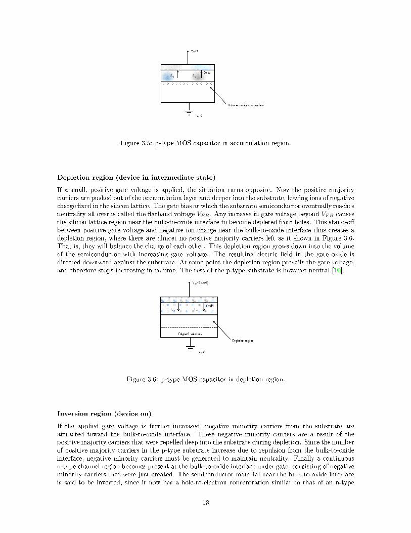
Figure 3.5: p-type MOS capacitor in accumulation region.
Depletion region (device in intermediate state)
If a small, positive gate voltage is applied, the situation turns opposite. Now the positive majoritycarriers are pushed out of the accumulation layer and deeper into the substrate, leaving ions of negativecharge xed in the silicon lattice. The gate bias at which the substrate semiconductor eventually reachesneutrality all over is called the atband voltage VFB . Any increase in gate voltage beyond VFB causesthe silicon lattice region near the bulk-to-oxide interface to become depleted from holes. This stand-obetween positive gate voltage and negative ion charge near the bulk-to-oxide interface thus creates adepletion region, where there are almost no positive majority carriers left as it shown in Figure 3.6.That is, they will balance the charge of each other. This depletion region grows down into the volumeof the semiconductor with increasing gate voltage. The resulting electric eld in the gate oxide isdirected downward against the substrate. At some point the depletion region prevails the gate voltage,and therefore stops increasing in volume. The rest of the p-type substrate is however neutral [10].
Figure 3.6: p-type MOS capacitor in depletion region.
Inversion region (device on)
If the applied gate voltage is further increased, negative minority carriers from the substrate areattracted toward the bulk-to-oxide interface. These negative minority carriers are a result of thepositive majority carriers that were repelled deep into the substrate during depletion. Since the numberof positive majority carriers in the p-type substrate increase due to repulsion from the bulk-to-oxideinterface, negative minority carriers must be generated to maintain neutrality. Finally a continuousn-type channel region becomes present at the bulk-to-oxide interface under gate, consisting of negativeminority carriers that were just created. The semiconductor material near the bulk-to-oxide interfaceis said to be inverted, since it now has a hole-to-electron concentration similar to that of an n-type
13

material. The device is at present thus in inversion region as shown in Figure 3.7. The depletedarea below the channel is still present irrespective of the conducting channel, but it does not increase.Instead, the increase in gate voltage is balanced by the increase in attracted negative minority carriers.The gate voltage at which this channel is created is called the threshold voltage VTH as mentioned insection 2.2. The actual threshold voltage is determined by the doping prole of the substrate. Theresulting electric eld is still directed downward against the substrate. It is common to divide thisregion into the two sub-regions weak inversion and strong inversion, which refer to the regions beforeand after Vth respectively. Hence the threshold voltage indicates the point at which strong inversion isreached.By adding n-type drain and source diusions on each side of the MOS capacitor structure, thecharge concentration at the bulk-to-oxide interface described above determines the condition betweenthese two diusions. When the device is o, the p-type region between the two diusions acts as abarrier since it is of opposite polarity. But when the channel is present, the charge concentration atthe bulk-to-oxide interface is on the other hand of the same polarity as that of the diusions. Hencethere is a direct path between drain and source where current may ow, since these minority carriersare mobile [10, 12].
Figure 3.7: p-type MOS capacitor in inversion region.
3.2.2 MOSFET parasitic capacitances
The parasitic capacitances of the MOSFET make up an important part of the total parasitic ca-pacitance of a specic design in addition to the interconnect delays. Analysis of MOSFET parasiticcapacitances is also an often-used method for characterizing a specic MOSFET technology. Thisis done by measuring the MOSFET equivalent capacitance, and from this vital information can beextracted. Among the MOSFET device and process parameters which can be found from CV mea-surements are gate oxide thickness tox and threshold voltage VTH . Capacitances associated with theMOSFET is typically classied into two major groups: oxide-related capacitances and junction capac-itances. The former comes as a consequence of the gate oxide acting as a dielectric between variouselectrodes of the MOSFET, and will be discussed in section 3.2.3. While the latter is a result of thedepletion region formed between the p-n junctions within the semiconductor material, acting as adielectric between the diusions and bulk. Junction capacitances will not be studied as part of thisthesis [14].
3.2.3 The MOS capacitor
A simplistic drawing of a silicon-based MOS Capacitor is shown in Figure 3.8. It consists of dopedsilicon as the substrate, a gate electrode made of polycrystalline silicon, and silicon dioxide (symbolSiO2) to separate gate from the substrate. The MOS capacitor actually consists of two dierentcapacitors. These are the gate capacitance per unit area C ′ox and the channel junction capacitanceCjc. The dielectric of C
′ox is the always existing gate oxide, while the dielectric of Cjc is the depleted
region created in the semiconductor during depletion. We can also dene,
14

C ′ox =εSiO2
tOX(3.1)
where εSiO2 is the permittivity of silicon dioxide and tox is the oxide thickness[15].By assuming a unit sized MOS capacitor, C ′OX is shared between various electrodes according to
the mode of operation:
Cgg: is the total capacitance of a MOS capacitor seen from the gate,
Cgb: is the capacitance between gate and body (Substrate).
Figure 3.8: Equivalent circuit for the capacitances represented by the MOS Capacitor.
3.2.4 MOSFET Oxide-related capacitances and COX extraction methodology
The MOSFET oxide-related capacitances arise mainly due to a decomposition of the MOS capacitortotal gate capacitance Cgg. We expect that a capacitance exists between every two of the four terminalsof a MOSFET as shown in Figure 3.9. The value of each of these capacitances depend on the the regionof operation for the MOSFET as we discussed in the section 3.2.1 for the MOS capacitor [5].
Figure 3.9: MOS capacitances.
Consider the terminal connections of n-channel MOSFET shown in Figure 3.9, a bias is appliedto the gate terminal. Depending upon the gate bias there are dierent regions of operation in C-Vcurve that are accumulation, depletion and inversion as described in details for the MOS capacitor
15

in section 3.2.1.So, in accumulation region of operation the gate to source bias is negative because ofthe holes from the substrate are attracted under the gate region as described above.Therefore, thereare three types of capacitances are involved that are capacitance between gate electrode and substrate(Cgb), capacitance between gate and drain terminals (Cgd) and capacitance between gate and sourceterminals (Cgs). In case that, VGS is positive but less than VTH for some terminal biases, the surfaceunder the gate is depleted because the holes under the gate are displaced and leave negative immobileions that contribute to negative. In this region of operation the capacitance between the gate andthe source/drain is simply overlap capacitance while the capacitance between the gate and substrateis the oxide capacitance in series with depletion capacitance of the formed of depletion region. TheMOSFET operated in this region is said to be in weak inversion or the sub threshold region. Finally,when VGS is suciently positive and is larger than VTH then a large number of electrons are attractedunder the age and the surface is said to be inverted. In integrated circuits the capacitor based onMOSFETs are designed in this region of operation. As a result, from the Figure 3.10 which shows thetotal gate capacitance Cgg versus the gate voltage VG we can assume that COX is extracted from theinversion part of this plot [16]. Also, we can dene C ′OX by deviding COX by the aspect ratio W/L,
C ′OX =COXWL
(3.2)
Figure 3.10: Cgg vs. VG - NMOS transistor COX extraction methodology.
3.2.5 Simulation and results
In this section, simulated gate capacitance cgg vs. gate voltage VG for W/L = 500nm/500nm insaturation (| VDS |= 1.2V ) for NMOS and PMOS of 65nm, 90nm bulk CMOS technologies are pre-sented in Figure 3.11. Alsο, from the schematic of the circuit in Figure 3.34 and following the extractmethodology mentioned above, we can see a summary of the results for the simulated PDKs in theTable 1.
Parameter Simulated (PDK 90nm) Simulated (PDK 65nm) Unit
COX (NMOS) / C ′OX (NMOS) 3.07/12.3 3.37/13.5 fF / fF/µm2
COX (PMOS) / C ′OX (PMOS) 2.93/11.7 3.14/12.6 fF / fF/µm2
Table 1: COX , C′OX simulated values for (a) n-type and (b) p-type MOSFETs of 65nm, 90nm bulk
CMOS process.
16

a) b)
Figure 3.11: Simulated gate capacitance cgg vs. gate voltage VG (W/L = 500nm/500nm) in saturation(| VDS |= 1.2V ) for (a) n-type and (b) p-type MOSFETs of 65nm, 90nm bulk CMOS process.
3.3 Slope factor n and technology current I0 extraction
3.3.1 Slope factor n denition
One more parameter for the characterization of MOS transistors is the slope factor or weak inversionslope n. The ideal slope factor is equal to one, the bulk MOS transistor, however, is characterizedby a slope factor a few percent to tens of percent higher than one with nominal values from 1.2 to1.7 depending on the bulk CMOS process. The reason for the deviation from the ideal slope factor inthe bulk transistor is that a change in the gate voltage is not only accompanied by a change in theinversion charge but also by a change in the bulk charge [6]. The amount of substrate factor n appearsto aect the current ow through MOSFET in all operating areas. Using n we try to approximatethe eect of the substrate on the electric eld that develops between the gate and the channel. Thesubstrate coecient is dened as shown below,
n ≡ ∂VG∂VP
= 1 +γ
2√VP + φ
(3.3)
where, φ is the approximation of the surface potential, γ is the is the body eect factor and VP is thepinch o voltage which corresponds to the value of the channel potential Vch for which the inversioncharge becomes zero in a non-equilibrium situation. The pincho voltage mainly depends on gatepotential VG and an eective approximation could be,
VP ∼=VG − VTO
n, (3.4)
where VTO is the threshold voltage at VS = 0 [17, 18].
3.3.2 Technology current I0 denition
A key design parameter in analog CMOS design done in submicron CMOS technology is the MOSFETinversion coecient IC (Inversion Factor). A design methodology that is based on the universal shapeof the transconductance eciency gm
IDvs. IC curve is very common and we will analyze it further in
section 3.4. IC is ID, the DC drain current of the MOS device, normalized by the shape factor W/Lwhich is also known as the MOSFET aspect ratio and a xed process technology current I0 [7],
iC =ID
I0(WL ), (3.5)
where
I0(W
L) = ISPEC , (3.6)
17

ISPEC is the normalization factor for the current, which is named specic current. We also know that
I0 = 2nU2TµC
′OX . (3.7)
When W = L, from 3.7,I0 = ISPEC (3.8)
.
3.3.3 Slope factor n and technology current I0 extraction methodology
Both, the specic current I0 and slope factor n need to be calculated. This can be done in var-ious ways. We will demonstrate the approach which exploits the characteristics of the normalizedtransconductance-to-current ratio gmUT
ID. We know that when W = L, specic current ISPEC is equal
to the technology current I0. We also know that, in saturation, there is a direct relation between thenormalized tranconductance-to-current ratio and the drain current,
gmUTID
=1√
14 + ID
ISPEC+ 1
2
, (3.9)
setting IDISPEC
= 1,
1√14 + ID
ISPEC+ 1
2
= 0.618,
So,
I0 = 0.618((gmUTID
)|max. (3.10)
Finally, slope factor n is can extracted from the maximum gmUT
IDvs. ID plateau in weak inversion
according to,
n =1(
gmUT
ID|max
) (3.11)
Figure 3.12 demonstrates normalized transconductance-to-current ratio gmUT
IDvs. drain current ID
(W/L = 1), with the x-axis in logarithmic scale in order to show how specic current ISPEC andslope factor n are extracted.
Figure 3.12: gmUT
IDvs. ID(W/L = 1) - NMOS transistor n, I0 extraction methodology.
18

3.3.4 Simulation and results
In this section, Figure 3.13 shows the simulated normalized transconductance-to-current ratio gmUT
IDvs. drain current ID (W/L = 500nm/500nm) in saturation (| VDS |= 1.2V ) for NMOS and PMOSof 65nm, 90nm bulk CMOS technologies. Also, from the schematic of the circuit in Figure 3.35and following the extract methodology described above, we can see a summary of the results for thesimulated PDKs in the Table 2.
Parameter Simulated (PDK 90nm) Simulated (PDK 65nm) Unit
nn (NMOS) 1.24 1.25 −np (PMOS) 1.22 1.24 −I0,n (NMOS) 630 390.25 nAI0,p (PMOS) 330 346 nA
Table 2: n, I0 simulated values for (a) n-type and (b) p-type MOSFETs of 65nm, 90nm bulk CMOSprocess.
a) b)
Figure 3.13: Simulated normalized transconductance-to-current ratio gmUT
IDvs. dran current ID
(W/L = 500nm/500nm) in saturation (| VDS |= 1.2V ) for (a) n-type and (b) p-type MOSFETsof 65nm, 90nm bulk CMOS process.
Both technologies show similar trend and weak inversion plot prediction. In the case of NMOSdevices a slight dierence is noticed in moderate inversion whereas in the case of PMOS, the weakinversion slope is almost identical in all cases.
3.4 Carrier mobility µ and transconductance parameter Kp
3.4.1 Carrier mobility µ denition
One of the most important parameters for all semiconductor devices is the mobility of the carrierowing inside the channel. Their mobility, also known as their ability to move through the crystal,will dene the electrical performances of the device. The mobility is consequently a paramount pa-rameter, and its good knowledge is of prime importance to rst understand the physics underlying theconduction mechanisms inside semiconductor devices and second to be able to model and simulate asingle transistor and in turn more complex circuits. Carrier mobility µ, in MOSFET transistors is afactor which refers to the mobility of electrons and holes in the channel between drain and source ter-minals. The eective mobility as a function of electric eld, substrate doping, and temperature is used
19

to determine the various mobility components (surface roughness, phonon, and coulombic scatteringlimited mobility components. Therefore, the channel mobility µ can be calculated from [22, 23]:
1
µ=
1
µC+
1
µPH+
1
µSR, (3.12)
where µC,µPH,µSR are the mobility components mentioned above.
3.4.2 Transconductance parameter Kp denition
The process transconductance Parameter KP is a constant that depends on the process technologyused to fabricate an integrated circuit. Therefore, all the transistors on a given substrate will typicallyhave the same value of this parameter [1]. The transistor's transconductance parameter KP is obtainedby multiplying mobility µ by the oxide capacitance C ′OX ,
KP = µC ′OX . (3.13)
3.4.3 Transconductance parameter Kp and carrier mobility µ extraction methodology
In order to extract transconductance parameter Kp in saturation, we can use the following sequenceof equations:
ID =β
2n[VG − VTO − nVS ]2 (3.14)
and by applying the derivative of VG over√ID the result is:
∂√ID
∂VG=
√β
2n. (3.15)
Furthermore,
β = µC ′OXW
L(3.16)
and from 3.13, 3.16, solving for KP , the initial equation becomes,
KP = (∂√ID
∂VG)22n
L
W. (3.17)
Finally, we can easily derive mobility µ from the equation 3.13 as follows,
µ =KP
C ′OX. (3.18)
20

3.4.4 Simulation and results
In this section, Figure 3.14, shows simulated transconductance parameter Kp vs. channel length Lin saturation (| VDS |= 1.2V ) for NMOS and PMOS of 65nm, 90nm bulk CMOS technologies. Theschematic of the circuit used to derive these results is depicted in Figure 3.36 and the summary of theresults are also found in the Table 3.
Parameter Simulated (PDK 90nm) Simulated (PDK 65nm) Unit
KP,n (NMOS) 306 252 µAV 2
KP,p (PMOS) 103 102 µAV 2
µn (NMOS) 249 187 cmV s
µp (PMOS) 88 81 cmV s
Table 3: KP ,µ simulated values for (a) n-type and (b) p-type MOSFETs of 65nm, 90nm bulk CMOSprocess.
a) b)
Figure 3.14: Simulated transconductance parameter Kp vs. channel length L (W = 500nm) in satu-ration (| VDS |= 1.2V ) for (a) n-type and (b) p-type MOSFETs of 65nm, 90nm bulk CMOS process.
For the n-type MOSFETs, the 90nm PDK predicts higher Kp values versus channel length L,when compared to the 65nm PDK. The p-type devices show the opposite behavior towards higherchannel lengths. Therefore mentioned dierences can be partially attributed to the dierent Cox valuespredicted from the the tow dierent pdk 's. It has to be mentioned than in all cases, as expected, theKp values are approximately ∼ 3 times higher for n-type MOS devises when compared to those of thePMOS counter parts.
3.5 Transconductance eciency gmID
and transit frequency fT extraction
3.5.1 MOS Transconductance gm denition
A MOSFET operating in saturation produces a current in response to its gate-source overdrive voltage,which is is dened as the voltage between transistor gate and source VGS in excess of the thresholdvoltage VTH where VTH is dened as the minimum voltage required between gate and source to turnthe transistor on as it is referred above. So it would be useful to dene a gure of merit that indicateshow well a device converts a voltage to a current. More specically, since in processing signals, we'reinterested in the changes in voltages and currents, we dene the gure of merit (FoM) as the changein the drain current divided by the change in the gate-source voltage. This is called transconductanceand usually dened in the saturation region, denoted by gm,
21

gm =∂ID∂VGS
|VDSconst.∼= (3.19)
KPW
L(VGS − VTH). (3.20)
Therefore, gm sets the sensitivity of the device, for a high gm, a small change in VGS results in a largechange in ID. The SI unit, the Siemens, with the symbol, S, 1 Siemens = 1 ampere per volt replacedthe old unit of conductance, having the same denition, the (ohm spelled backwards), symbol,M. Inanalog design, we sometimes say a MOSFET operates as a transconductor to indicate that it convertsa voltage change to a current change. So, gm in the saturation region is equal to [5],
gm ∼= KPW
LVOV , (3.21)
from the following approximate equation for the drain current
ID =KP
2
W
L(VGS − VTH)2, (3.22)
we can dene again gm as,
gm ∼=√
2KP (W
L)|ID| ∼= (3.23)
2IDVOV
. (3.24)
a) b) c)
Figure 3.15: Approximate MOS transconductance as a function of overdrive and drain current.
We can easily obsverve that, gm increases with the overdrive if W/L is constant, whereas 3.24implies that gm decreases with the overdrive if ID is constant.
3.5.2 Transit frequency fT denition
Transit frequency fT is dened as the frequency at which the extrapolated small-signal current gainof the transistor in CS conguration falls to unity. fT is a widely used metric for characterizing thehigh-frequency behavior of a MOSFET because many performances, such as the gain and the minimumnoise factor, are directly linked to fT . A good approximation of fT is given by [26],
fT =gm
2πCgg, (3.25)
where Cgg is the total gate capacitance. Both gm and Cgg, are bias dependent, so fT is bias dependenttoo. So, we can express fT as a function of inversion factor and channel length as follows,
22

fT =µUT
2πL2eff
(√
1 + 4IC − 1). (3.26)
Therefore, from 3.26 we can easily conclude that, assuming a constant mobility, fT increases linearlywith IC in weak inversion before increasing with
√IC in strong inversion and also for a given IC , fT
decreases as 1/L2 with increasing channel length for all regions of operation.
3.5.3 Transconductance eciency gmID
extraction as a Figure of Merit (FoM)
The transconductance eciency gmID
FoM is one of the most important performance metrics for analogcircuit design. It is a measure of how much transconductance is produced for a given bias currentand is a function of IC . The transconductance eciency (or its inverse) appears in many expressionsrelated to the power optimization of analog circuits. In the normalized form, we have already used itin section 3.3.3 in order to extract slope factor n and technology current I0[26]. We can easily extractthe transconductance eciency if we simply divide the equation 3.19 with the drain current. We plottransconductance eciency relative to the inversion coecient IC , which is dened by the equation3.5. The shape of the transconductance eciency curve is universal for MOS operation as it shownin Figure 3.16 and is channel length and process independent until velocity saturation eects reducetransconductance eciency. These characteristics provide important information to the designer, andthey also constitute particularly dicult benchmark tests for the accuracy and adequacy of compactMOS models.
Figure 3.16: NMOS transistor transconductance eciency gmID
(in log-log scale) typical representata-tion.
3.5.4 Transconductance eciency multiplied by transit frequency gmfTID
extraction as aFigure of Merit (FoM)
Both gmID
and fT are very important FoMs of analog/RF design. The former characterizes the dcperformance of a device while the latter characterizes its high-frequency performance. Nevertheless,exists a fundamental tradeo between the two. Aiming for low-power operation by targeting a highgmID
at small values of IC invariably means compromising in speed (bandwidth). This is where theFoM dened as the product of the two formerly dened metrics comes into the picture. Combiningtwo quantities that have their maxima on the opposite ends of the IC axis, the gmfT
IDFoM serves as
design guide to locate the optimum IC . Figure 3.17 shows a behavior that makes it useful for locatingthe optimum IC . This maximum is peak lies at the higher end of the MI region for the contemporaryCMOS technologies and moves deeper into the MI region with decreasing channel lengths [26].
23

Figure 3.17: NMOS transistor transconductance eciency multiplied by transit frequency gmfTID
(inlog-log scale) typical representatation.
3.5.5 Simulation and results
In this section, three dierent types of transconductance eciency gures are presented. At rst, Figure3.18 presents the simulated transit frequency fT vs. inversion coecient IC (W/L = 500nm/500nm)from weak to strong inversion in saturation (| VDS |= 1.2V ) for (a) n-type and (b) p-type MOSFETs of65nm, 90nm bulk CMOS process. Figure 3.19 shows the simulated transconductance-to-current-ratiogmID
vs. inversion coecient IC (W/L = 500nm/500nm) from weak to strong inversion in saturation(| VDS |= 1.2V ) for (a) n-type and (b) p-type MOSFETs of 65nm, 90nm bulk CMOS process. In Figure3.21, the simulated transconductance eciency multiplied by transit frequency gmfT
IDvs. inversion
coecient IC (W/L = 500nm/500nm) from weak to strong inversion in saturation (| VDS |= 1.2V ) for(a) n-type and (b) p-type MOSFETs of 65nm, 90nm bulk CMOS process, is also presented. Finally,Figure 3.20 and Figure 3.20 show the transconductance eciency gm
IDvs. inversion coecient IC
(W/L = 500nm/500nm) from weak to strong inversion in saturation as parametric sweep for dierentL characteristics (W/L = 500nm/500nm) for (a), (c) n-type and (b), (d) p-type MOSFETs for both90nm and 65nm bulk CMOS technologies. The schematic of the circuit used to derive these results isdepicted in Figure 3.37.
a) b)
Figure 3.18: Simulated transit frequency fT vs. inversion coecient IC (W/L = 500nm/500nm) fromweak to strong inversion in saturation (| VDS |= 1.2V ) for (a) n-type and (b) p-type MOSFETs of65nm, 90nm bulk CMOS process.
24

a) b)
Figure 3.19: Simulated transconductance-to-current-ratio gmID
vs. inversion coecient IC (W/L =500nm/500nm) from weak to strong inversion in saturation (| VDS |= 1.2V ) for (a) n-type and (b)p-type MOSFETs of 65nm, 90nm bulk CMOS process.
a) b)
c) d)
Figure 3.20: Simulated transconductance-to-current-ratio gmID
vs. inversion coecient IC (W/L =500nm/500nm) from weak to strong inversion in saturation (| VDS |= 1.2V ) (parametric sweep fordierent L) characteristics (W/L = 500nm/500nm) for (a), (c) n-type and (b), (d) p-type MOSFETsof 65nm, bulk CMOS process.
25

a) b)
Figure 3.21: Simulated transconductance-to-current-ratio multiplied by transit frequency gmfTID
vs.inversion coecient IC (W/L = 500nm/500nm) from weak to strong inversion in saturation (| VDS |=1.2V ) for (a) n-type and (b) p-type MOSFETs of 65nm, 90nm bulk CMOS process.
Transconductance to current ratio in all cases follow the expected behavior. For both n and p-type MOSFETs, the two dierent PDKs show identical results. The simulated transient frequencypresents slightly increased value in the case of the n-type MOSFETs of the 90nm PDK. Therefore,transconductance-to-current-ratio multiplied by transit frequency gmfT
IDpresent an increased value
towards SI for the case of the n-type MOSFETs. It can be noticed that both PDKs predict similarbehavior vs.. inversion coecient (IC) for the case of p-type MOSFETs.
3.6 Early Voltage Ua extraction
3.6.1 Output conductance gds in saturation and early voltage denitions
In the design of CMOS analog circuits, the Early voltage (or the output conductance) of a transistorin saturation is a fundamental parameter since it aects, for example, the accuracy of current mirrorsand the gain of voltage ampliers. In the circuit-design-oriented approach, the simplest model of theoutput conductance assumes it to be proportional to the drain current and inversely proportional tothe Early voltage VA as given below,
gds =∂ID∂VD
=IDVA
. (3.27)
VA is a constant parameter in rst-order models. However, a constant Early voltage is inadequate tomodel the output conductance for the simulation of analog circuits. An improved model of the Earlyvoltage considers it to be proportional to the channel length and independent of both current leveland drain voltage,
Ua =VAL. (3.28)
In this case, the output conductance is simply,
gds =IDUaL
. (3.29)
Even though this model of the output conductance is not accurate, it provides a simple expressionto quickly evaluate how the transistor output conductance is aected by the drain current and thechannel length [28]. Approximation 3.29 will be extensively used throughout this thesis.
3.6.2 Early voltage Ua extraction methodology
Figure 3.21, illustrates MOS drainsource conductance calculation using the early voltage. A tangentline is drawn touching the ID versus VDS curve at the bias point (we express the MOS bias point interms of the inversion coecient, which is near the onset of strong inversion), and this line intersects
26

the VDS axis at the early voltage. The drainsource conductance, gds, is the slope of the tangent linegiven by the drain bias current, ID, divided by the sum of the early voltage, VA, and drainsource biasvoltage, VDS . Frequently, as throughout this thesis, VDS is included in VA as shown in equation 3.27,where gds is not a constant value for the process, but depends upon the channel length, inversion level,and VDS [7].
Figure 3.22: ID vs. VDS(W/L = 1)- NMOS transistor Ua extraction methodology.
3.6.3 Simulation and results
In this section, Figure 3.23, shows simulated early voltage Ua vs. channel length L (W = 500nm)in saturation (| VDS |= 1.2V ) for NMOS and PMOS of 65nm, 90nm bulk CMOS technologies. Theschematic of the circuit used to derive these results is depicted in Figure 3.38 and the summary of theresults are also found in the Table 4.
Parameter Simulated (PDK 90nm) Simulated (PDK 65nm) Unit
VA,n (NMOS) /Ua,n (NMOS) 4.028/8.057 5.18/10.37 mV / Vµm
VA,p (PMOS) /Ua,p (PMOS) 4.024/8.049 6.27/12.53 mV / Vµm
Table 4: Ua simulated values for (a) n-type and (b) p-type MOSFETs of 65nm, 90nm bulk CMOSprocess.
27

a) b)
Figure 3.23: Simulated early voltage Ua vs. channel length L (W/L = 500nm/500nm) in saturation(| VDS |= 1.2V ) for (a) n-type and (b) p-type MOSFETs of 65nm, 90nm bulk CMOS process.
Early voltage Ua is increased towards shorter channel lengths values in all cases. For both n- andp-type MOSFETs, the 90nm 65nm PDK predicts slightly increased values.
3.7 Intrinsic gain AV extraction
3.7.1 Intrinsic gain AV denition and extraction methodology
Maximum gain of a single MOSFET transistor is called intrinsic gain, and is equal to [5],
AV = gmr0, (3.30)
where gm is the transconductance as dened above, and r0 is the output resistance of transistor, whichwe can easily dene as,
r0 =1
gds. (3.31)
So, from the equations 3.19, 3.27 the intrinsic gain of a MOSFET is dened as the ratio,
AV =gmgds
, (3.32)
dividing both gds and gm by drain current and due to the equation 3.29, we conclude that,
AV =
gmIDgdsID
= UaLgmID
. (3.33)
Therefore, as we have already extract early voltage and transconductance, we can use the equation3.33 to extract intrinsic gain as well. Finally, as we can easily observe, intrinsic gain AV is directlyproportional to the channel length of transistors. In ampliers, one can increase channel length inorder to get higher output resistance and gain as well. But, it will also increase parasitic capacitanceof transistor, which will limit the bandwidth of amplier. Channel length of transistors become smallerin modern CMOS technologies, and makes achieving high gain in an amplier very challenging. Inorder to achieve high gain, there are many techniques we can follow. In the following sections, we willhave a brief look to dierent topologies of transconductance ampliers, and their features.
3.7.2 Simulation and results
In this section, Figure 3.24, shows simulated intrinsic gain AV = gmgds
vs. inversion coecient IC(W/L = 500nm/500nm) from weak to strong inversion in saturation (| VDS |= 1.2V ) for NMOS andPMOS of 65nm, 90nm bulk CMOS technologies. The schematic of the circuit used to derive theseresults is depicted in Figure 3.38. For the given PDKs, the intrinsic gain is shown as a function of theinversion factor. Obviously, longer L provides larger gain. The key point here is to notice that when
28

transistor operates in the center of moderate inversion, the gain value almost approaches its maximum,and thus it may often be an optimal design choice.
a) b)
Figure 3.24: Simulated intrinsic gain AV = gmgds
vs. inversion coecient IC (W/L = 500nm/500nm)
from weak to strong inversion in saturation (| VDS |= 1.2V ) for (a) n-type and (b) p-type MOSFETsof 65nm, 90nm bulk CMOS process.
For the given PDKs, the intrinsic gain is shown as a function of the inversion factor. Obviously,longer L provides larger gain. The key point here is to notice that when transistor operates in thecentre of moderate inversion, the gain value almost approaches its maximum, and thus it may often bean optimal design choice. In all cases, the predicted intrinsic gain AV is improved in the 65nm PDK.For both n- and p-type transistors, the intrinsic gain values is relatively close for PDKs.
3.8 Flicker or 1/f noise extraction
3.8.1 Noise in MOSFETs
Noise limits the minimum signal level that a circuit can process with acceptable quality. Today, interms of analog design we are constantly dealing with the problem of noise because it trades with powerdessipation, speed and linearity. In this section, we are going to describe the phenomenon of noiseand specically icker noise and its eect on analog circuits. Noise is generated in all semiconductordevices and is perceived as spontaneous random uctuations in current or in voltage [5]. Followinga general description of noise characteristics in the frequency and time domains, we can say that inMOSFETs there are several noise mechanisms coming from the channel of the device, related to localrandom uctuations of the carrier velocity or the carrier density and they are observed over variousfrequency ranges [30]. More specically, we can dene four types of noise sources: Thermal noise, lowfrequency noise (LFN) or 1/f noise, generation-recombination noise (RTS) and Shot noise. Therefore,the total noise is a superinduction of all noise sources. It should also be mentioned that in frequencydomain noise can be described by the Power Spectral Density (PSD) which shows how much power asignal carries at each frequency and is expressed in V 2/Hz or Watt/Hz [31].
3.8.2 Flicker or 1/f noise denition and extraction methodology
Flicker noise is a low-frequency noise and is probably the most important, and most misunderstood,noise source in CMOS circuit design. Flicker noise is also known as 1/f noise pronounced one overf because its PSD, as we shall see, is inversely proportional to frequency [4]. The interface betweenthe gate oxide and the silicon substrate in a MOSFET entails an interesting phenomenon, since thesilicon crystal reaches an end at this interface, many dangling bonds appear, giving rise to extraenergy states. As a result, charge carriers move at the interface, some are randomly trapped and laterreleased by such energy states, introducing icker noise in the drain current. In addition to trapping,several other mechanisms are believed to generate icker noise [5]. The average power of icker noisecannot be predicted easily, depending on the of the oxide-silicon interface, icker noise may assumeconsiderably dierent values and as such varies from one CMOS technology to another. The icker
29

noise is more easily modeled as a voltage source in series with the gate and, in the saturation region,is given by
SV G,FLICKER =KF
C2OXWLfAF
, (3.34)
where KF is the icker noise factor having units of C2/cm2 , and AF is the frequency exponent, whichhas been added to consider the deviation from the ideal 1/f slope. KF typical values ranging from10−33 to 10−29 C2/cm2 [7].
In order to understand better how we extract icker noise from total noise diagram, in Figure 3.24the expected pattern of the drain-referred noise current PSD is depicted.
Figure 3.25: Typical drain-referred noise current PSD of a MOSFET.
Thermal noise has no dependence on frequency and so is at a while low icker noise, comes with apower spectra density inverse proportional to the frequency and is dominant in frequencies lower thanthe corner frequency (fc), where thermal noise and icker noise have equal PSDs [32, 33]. Flicker noisecan be represented as drain current noise source (output referred noise) SID, or gate voltage noisesources (input referred noise) SV G as shown in Figure 3.26.
a) b)
Figure 3.26: MOS noise model showing (a) drain-referred noise current and (b) gate-referred noisevoltage sources along with a gate noise current source.
Output noise is measured as in this work and input noise is calculated. The expressions used forthe PSD conversion between drain-referred and gate-referred noise sources are,
SID = SV Ggm2(A/√Hz) (3.35)
30

and
SV G =SIDg2m
(V/√Hz), (3.36)
where gm is the gate transconductance in Siemens.As standard for noise sources, the noise sources are characterized using the power spectral density
(PSD) or noise power in a 1Hz bandwidth.
3.8.3 Simulation and results
In this section, Figure 3.27, shows the simulated drain-referred noise noise SID vs. frequency (W/L =500nm/500nm) from weak to strong inversion in saturation (| VDS |= 1.2V ) for (a) n-type and (b)p-type MOSFETs for both 90nm and 65nm bulk CMOS technologies. Also, Figure 3.28 presents thesimulated gate- referred noise voltage source noise SV G vs. frequency (W/L = 500nm/500nm) fromweak to strong inversion in saturation (| VDS |= 1.2V ) for (a) n-type and (b) p-type MOSFETs of65nm, 90nm bulk CMOS process. The schematic of the circuit used to derive these results is depictedin Figure 3.39.
a) b)
Figure 3.27: Simulated drain-referred noise SID vs. inversion coecient in saturation (| VDS |= 1.2V ),for (a) n-type and (b) p-type MOSFETs, of 65nm and 90nm bulk CMOS process.
a) b)
Figure 3.28: Simulated gate-referred noise SV G vs. inversion coecient in saturation (| VDS |= 1.2V ),for (a) n-type and (b) p-type MOSFETs, of 65nm and 90nm bulk CMOS process.
Output noise SID, follow the expected trend versus inversion coecient. For both technologiesmarginally dierences can be observed versus the inversion coecient. Output noise is minimum inweak inversion and increasing to reach its maximum value towards strong inversion. In the case ofPMOS devices 90nm PDK predicts bigger LFN values when compared to the 65nm PDK. This can bepartially attributed to the minor dierence of normalized transconductance eciency.
31

3.9 Current and voltage MOSFET mismatch σ( δIDID
), σ(δVG) extraction
3.9.1 Mismatch denition
Mismatch is an eect that arises in IC fabrication and is a limiting factor of the accuracy and reliabilityof many analog and digital integrated circuits. Due to mismatch two equally designed transistorsdisplay dierent electrical behavior. The main reason for the dierences is the non-uniformity ofprocess parameters across the wafer. Mismatch aects electrical parameters of the transistor, whichin turn dier between two identically devices. Consequently the operating point and other circuitcharacteristics dier from their desired values [34]. Mismatch is the result of either systematic orstochastic (random) eects. Systematic eects are originated by either uncontrollable variation duringthe fabrication of the integrated circuit or by poor layout. At the origin of systematic mismatch canbe equipment-induced non-uniformities such as temperature gradients and photo-mask size dierencesacross the wafer. Systematic eects are important for large distances and can be combated usingappropriate layout techniques. Random mismatch refers to local variation in parameters such asdoping concentration, oxide thickness, polysilicon granularity, edge irregularity, etc. The rst threeuctuations are called areal uctuations because they scale with device area while the last one is calledperipheral uctuation because it scales with device perimeter. Random mismatch dominates oversystematic mismatch for small distances and is generally assumed to display a Gaussian distributioncharacterized by its standard deviation. Stochastic mismatch requires a model to orient the IC designerregarding sizing and biasing strategies [7, 35].
3.9.2 Current and voltage MOSFET mismatch σ( δIDID ), σ(δVG) denition and extractionmethodology
In order to dene current and voltage mismatch we examine two basic MOSFET topologies, a currentmirror and a dierential pair shown in Figure 3.28.
a) b)
Figure 3.29: Two basic MOSFET topologies: (a) a current mirror and (b) a dierential pair.
Theoretically, assuming that VT0 and β are uncorrelated, the square root of the normalized varianceof the drain current of saturated transistors having the same gate and source voltages as in the currentmirror of Figure 3.29(a) is given by,
σ(δIDID
) =
√σ2β + (
gmID
σT )2, (3.37)
where σβ resulting from the current-factor dierences between pairs of transistors ∆β (β = µCOXW/L)and is dened as,
σβ =Aβ√WL
, (3.38)
the typical values of Aβ , which do not change signicantly with technology-node scaling [36], rangefrom 1 μm to 3 μm. Also, the threshold voltage dierences ∆VTO modeled in the same way, thus,
σT =AT√WL
. (3.39)
32

The square root of the variance of the gate-voltage mismatch of two saturated transistors having thesame drain current and the same source voltage as in the dierential pair of Figure 3.29(b) is given by,
σ(δVG) =
√σ2T + (
gmID
σβ)2. (3.40)
For a current mirror, it can be seen from equation 3.37 that biasing the transistor in weak inversion(IC 1, and thus with the maximum gm
IDas shown in section 3.5.3 in Figure 3.16) results in the largest
current mismatch, whereas the minimum current mismatch, is obtained with the transistors operatingdeep in strong inversion [28]. On the other hand, for a dierential pair, for example, operation of thetransistors in weak inversion results in the minimum mismatch between the gate voltages, as shown inFigure 3.30(a)(b).
a) b)
Figure 3.30: NMOS transistor (a) current mismatch σ( δIDID ) and (b) voltage mismatch σ(δVG) vs.inversion coecient IC typical representation.
It should be noted that, in general, the design for best matching of a current mirror or a dierentialpair is more complicated than in the analysis above. In the design problem we must compare solutionscorresponding to transistors with dierent geometries and biases [28]. Mismatch can be simulated inseveral dierent ways. The goal of mismatch simulation is to obtain the standard deviation of circuitproperties caused by the stochastic nature of transistor model parameters. In this thesis, in orderto extract the current and voltage mismatch of the two basic MOSFET topologies shown in Figure3.29, we used simulation based on Monte-Carlo analysis, which is simple, precise and widely used.Several circuits with randomly chosen parameters according to the probability density function of thesimulated parameter are generated and simulated. The most frequently used distribution is Gaussianwhich was also used here but the method is appropriate for any kind of distribution [34]. So, for thisthesis using a special simulator tool (Cadence Virtuoso IC 6.15-ADEXL), we extracted the standarddeviation of the parameters we wanted for various IC values as we will see below.
3.9.3 Simulation and results
In this section, Figure 3.31, shows the simulated current mismatch σ( δIDID ) vs. inversion coecient IC(W/L = 500nm/500nm) from weak to strong inversion in saturation (| VDS |= 1.2V ) for (a) n-typeand (b) p-type MOSFETs for both 90nm and 65nm bulk CMOS technologies. In Figure 3.32, thesimulated voltage mismatch σ(δVG) vs. inversion coecient IC (W/L = 500nm/500nm) from weak tostrong inversion in saturation (| VDS |= 1.2V ) for (a) n-type and (b) p-type MOSFETs of 65nm, 90nmbulk CMOS process, is also presented. The schematics of the circuits used to derive these results aredepicted in Figures 3.40, 3.41.
33

a) b)
Figure 3.31: Simulated current mismatch σ( δIDID ) vs. inversion coecient IC (W/L = 500nm/500nm)from weak to strong inversion in saturation (| VDS |= 1.2V ) for (a) n-type and (b) p-type MOSFETsof 65nm, 90nm bulk CMOS process.
a) b)
Figure 3.32: Simulated voltage mismatch σ(δVG) vs. inversion coecient IC (W/L = 500nm/500nm)from weak to strong inversion in saturation (| VDS |= 1.2V ) for (a) n-type and (b) p-type MOSFETsof 65nm, 90nm bulk CMOS process.
Current mismatch is following the expected gmID
trend in all cases. Specically, drain current mis-match is expected to be maximum towards weak inversion. In the case of voltage mismatch the expectedbehavior is predicted, minimum values towards weak inversion for both n- and p-type transistors. The65nm PDK predicts improved matching in all cases.
34

3.10 Comparative results of the technology parameters
The Table 5 shows in detail the results of the extraction of the key design parameters of the twotechnologies 65nm and 90nm and their percentage change.
ParameterSimulated (PDK
90nm)Simulated (PDK
65nm)
Dierence betweenthe two
technologies (%)Unit
COX (NMOS) /C ′OX (NMOS)
3.07/12.3 3.37/13.5 +9.8 %fF /fF/µm2
COX (PMOS) /C ′OX (PMOS)
2.93/11.7 3.14/12.6 +7.2%fF /fF/µm2
nn (NMOS) 1.24 1.25 +0.8 % −np (PMOS) 1.22 1.24 +1.6 % −I0,n (NMOS) 630 390.25 -38 % nAI0,p (PMOS) 330 346 +4.8 % nA
KP,n (NMOS) 306 252 +17.6 % µAV 2
KP,p (PMOS) 103 102 -0.98 % µAV 2
µn (NMOS) 249 187 -24.9 % cmV S
µp (PMOS) 88 81 -7.9 % cmV S
VA,n (NMOS)/Ua,n (NMOS)
4.028/8.057 5.18/10.37 +28.7 % mV / Vµm
VA,p (PMOS)/Ua,p (PMOS)
4.024/8.049 6.27/12.53 +55.7 % mV / Vµm
Table 5: Basic design parameter extraction of of 65nm, 90nm bulk CMOS process and their percentagechange.
35

3.11 Cadence simulation schematics
All the schematic simulations (Cadence Virtuoso IC 6.15) used to extract the parameters analyzedabove are presented below.
a) b)
Figure 3.33: Transfer and output IDS − VGS , IDS − VDS schematic for (a) n-type and (b) p-typeMOSFETs.
a) b)
Figure 3.34: Oxide capacitance COX schematic for (a) n-type and (b) p-type MOSFETs.
a) b)
Figure 3.35: Slope factor n and technology current I0 schematic for (a) n-type and (b) p-type MOS-FETs.
36

Figure 3.36: Carrier mobility µ and transconductance parameter Kp schematic for n-type and p-typeMOSFETs [37].
Figure 3.37: Transconductance eciency gmID
and transit frequency fT schematic for n-type and p-typeMOSFETs [37].
37

Figure 3.38: Early Voltage Ua, intrinsic gain AV schematic for n-type and p-type MOSFETs [37].
a) b)
Figure 3.39: Flicker noise SID schematic for (a) n-type and (b) p-type MOSFETs.
a) b)
Figure 3.40: Current mismatch σ( δIDID ) schematic for (a) n-type and (b) p-type MOSFETs.
38

a) b)
Figure 3.41: Voltage mismatch σ(δVG) schematic for (a) n-type and (b) p-type MOSFETs.
39

4 Operational Transconductance Ampliers (OTAs)
Industry is continuously researching techniques to reduce power requirements, while increasing speed,to meet the demands of today's low (battery) powered wireless systems. The operational transcon-ductance amplier (OTA) is a fundamental building block in analog (mixed-signal) design and itsperformance characteristics are the foundation of system level characteristics. Improving the per-formance of the fundamental amplier structure, while avoiding costly silicon area and static powerincreases, is critical to improving system performance.
In this section of this thesis, we discuss general design ideas and techniques for a supply voltage of1.2V simple and fully dierential folded cascode OTA design and biasing in two dierent bulk CMOSprocesses of 65nm and 90nm. As we have already extract and verify the values of the most importantparameters of the two technologies in the previous section, the goal here is to exploit these results asmuch possible and use them in order to design properly these two circuits. After this process, using aprepared set of testbenches, circuits performances are veried by simulation in Cadence Virtuoso IC6.15 as in section 3 and as a result we can extract usefull conclusions for the two discussed technologies.
4.1 Basic theoretical Analysis of OTAs
The operational transconductance ampliers (OTAs) are ampliers whose dierential input voltageproduces an output current. Its ideal behavior is characterized by a high impedance input stage andhigh impedance output stage, as shown in Figure 4.1.
a) b)
Figure 4.1: a) Ideal OTA representation b) Small-signal equivalent circuit [39].
The ideal transfer function of this device is its transconductance, denoted by gm. The mainstructure of OTAs contains two stages. The rst one is a dierential input amplier, which producescurrent uctuations as a response to each input voltage (V+ and V−). The second stage is composedby current mirrors that mix this uctuations into an output current and also suppress the DC biascurrent. MOS technology is widely used in OTAs design due to its lower power consumption, itsdierential input innite impedance (even in open loop circuits) and the possibility of achieving verylow transconductances (in order of uS, nS and beyond) [38]. The transconductance response of thedierential input pair is not a linear function of its dierential input voltage. This is caused by theequations that describe the MOS transistors and their region of operation [40]. Since weak inversionregion is dominated by exponential relationships and strong inversion region by square-law formulas,moderate inversion is mostly recommended in OTA design since it oers the best trade-o betweenthe design parameters [41].
4.1.1 Basic analog structures
Structured analog design is based on the idea that an analog cell can be divided into basic analogstructures. A basic analog structure is a small analog building block consisting of one or more transis-tors. We can describe it by a set of design parameters that aect circuit performance. From this pointof view, the design procedure becomes the same for both simple and more complicated circuits. Thissection is focused on the basic analog structures used, in order to examine the circuit partitioning inthe section 4.1.2. A basic analog structure is described as a set of one or more transistors connectedin a specic way to realize voltage-to-current conversion, current-to-voltage conversion, or both. Sucha structure requires current or voltage bias, which is again realized by another basic analog structure.
40

Several basic analog structures connected together represent a more complex analog structure that isoften called an analog cell. In the Table below are shown the basic analog structures that are moreoften used in order to build an analog cell. It is crucial to note that a basic analog structure is notany combination of transistors [42].
Analog structure name Schematic Basic description
Common source
Common source (sourceconnected to the DC voltagesupply, the input at the gate,and the output at the drainterminal) structure, converts
voltage to current.
Common drain
Common drain (drain connectedto the DC voltage supply, theinput at the gate, and the
output at the source terminal)structure, converts voltage tocurrent and its the simplest
voltage follower.
Common gate
Common gate (gate connectedto the DC voltage supply, theinput at the gate, and the
output at the drain terminal)structure, converts voltage tocurrent and it has small input
impedance.
Diode-connectedtransistor
Diode-connected (gate anddrain connected together)
structure, converts voltage tocurrent.
Cascode
Cascode structure, is used involtage to current conversion, incommon source and gate stage
and it has high outputimpedance.
Folded cascode
Folded cascode structure, isused to convert voltage to
current and as a cascode stagevariant also.
Dierential pairDierential pair structure,
converts the dierential inputvoltage to current.
41

Cascoded dierential pair
Cascoded dierential pairstructure, converts the
dierential input voltage tocurrent and also used asdierential pair variant.
Folded cascodedierential pair
Folded cascoded dierential pairstructure, converts the
dierential input voltage tocurrent and also used as
dierential pair variant similarto simple cascoded dierential
pair.
Current mirror
Current mirror structure, copiescurrent through one active
device by controlling the currentin another active device of acircuit, keeping the output
current constant regardless ofloading and its also used forcurrent multiplication or
division [44].
Cascode current mirror
Cascode current mirrorstructure, copies current
precisely, it is used for currentmultiplication or division and ithas also high output impedance.
Table 6: Basic analog structures library [42].
Finally, we should note that except for the nite number of dierent basic analog structures, thereis also a nite number of transistor design situations. So, we could say that a basic analog structurerepresents a special case of transistor-level design, where each transistor works in the given environmentand only a few transistor design parameters are exist.
4.1.2 Circuit partitioning and behavioral model of an analog amplier
Usually, operational transconductance ampliers and operational ampliers designs implemented as asingle-ended or a fully-dierential topologies. The operational transconductance ampliers, realized assingle-stage ampliers which are classied as:
simple OTA,
telescopic OTA, and
folded cascode OTA.
Two-stage operational ampliers consist of an OTA in the rst stage followed by a common source, acommon drain or a cascode as illustrated in the same gure. Each stage of the analog amplier includesa transconductance (gm) structure that converts the input voltage to the output current, followed by a
42

load structure that converts the output current to the output voltage. The transconductance structureneeds a current bias, because any cascoded structure requires a voltage bias. Therefore, all basic analogstructures can be classied in the following way [42, 43]:
transconductance structures: common source, common drain, cascode, dierential pair andits cascoded variants,
load structures: simple and cascode current mirrors,
and bias structures: simple and cascode current mirrors, diode-connected transistor.
So, we can easily conclude that all transconductance structures have the same set of design parametersthat aect the circuit performances, which we will analyze in the section 4.1.3. This helps the derivationof the basic specications and simplies the design procedure of the circuits that we are going toanalyze.
When we refer to the behavioral model of an amplier, we assume tha there is a simplest gm-cellwhich includes the current bias structure and also provides the requires transconductance and theoutput current. This gm-cell followed by a load gives the simplest behavioral model of an analogamplier This model is useful, to do our system-level simulations for the derivation of the amplier'sspecications and it depends on the system and the application complexity. Two examples of behavioralmodels of an analog amplier which we will use with minor variations and in our simulations are shownin Figure 4.2.
a) b)
Figure 4.2: Behavioral model of an analog amplier with a) single-ended and b) fully-dierentialoutputs [42].
4.1.3 Denitions of the basic design parameters
Several common characterization methods are used to classify the functionality of OTA structures.These performance measurement techniques will be used to analyze designed structures via theoreticalcalculation and simulation with the procedures presented in the following chapters. A list of themeasured characteristics is provided below:
Gain- A0 [dB]
Gain Bandwidth product GBW [rad/s]
Phase Margin- PM [°]
Power consumption- P [W ]
Common-mode input range- CMR [V ]
Output-voltage swing- VOUT [V ]
Slew Rate- SR [V/s]
43

Noise [nV/√HZ ]
Oset- [mV ]
Open-loop gain (usually referred to as A0 [dB] ) is the gain of the amplier without the feedbackloop being closed, hence the name open-loop. This gain is at from dc to what is referred to asthe dominant pole. From there it falls o at 6dB/octave or 20dB/decade. (An octave is a doublingin frequency and a decade is x10 in frequency). This is referred to as a single-pole response. It willcontinue to fall at this rate until it hits another pole in the response. This 2nd pole will double therate at which the open-loop gain falls, that is, to 12dB/octave or 40dB/decade. If the open-loop gainhas dropped below 0dB (unity gain) before it hits the 2nd pole, the amplier will be unconditionalstable at any gain.
Figure 4.3: Open-Loop Gain (Bode Plot-single pole response).
The open-loop gain of each transconductance amplier stage is dened as a product of the equivalenttransconductance of the transconductance structure and the equivalent resistance seen at the output[42],
A0 = gmROUT (4.1)
The open-loop gain can change due to output voltage levels and loading. There is also some dependencyon temperature. In general, these eects are of a very minor degree and can, in most cases, be ignored[45].
Gain Bandwidth product for an amplier is the product of the amplier's bandwidth and the gainat which the bandwidth is measured [46]. The open-loop gain falls at 6 dB/octave. This means thatif we double the frequency, the gain falls to half of what it was. In other words, if the frequency ishalved, the open-loop gain will double, as shown in Figure 4.4. This gives rise to what is known as thegain bandwidth Product. If we multiply the open-loop gain by the frequency the product is always aconstant. The caveat for this is that we have to be in the part of the curve that is falling at 6 dB/octave.This gives us a convenient gure of merit with which to determine if a particular amplier is usablein a particular application [45]. The gain bandwidth product of a transconductance amplier stage isdened as the quotient of the the equivalent transconductance of the transconductance structure andthe equivalent maximal output capacitance of load structure [42],
GBW =gm
2πCL. (4.2)
Phase Margin is the amount of phase shift that is left until you hit 180 measured at the unity
gain point [45]. Just as the amplitude response does not stay at and then change instantaneously,
44

the phase will also change gradually, starting as much as a decade back from the corner frequency. Inorder to dene properly the connection between these three rst parameters it is mandatory to analyzeand explain the frequency response of an amplier. The poles and zeros in the transfer function can beeasily determined analyzing the gain path, i.e. the signal path from the amplier input to the amplieroutput, and using the following guidelines [5]:
pole- corresponds to an equivalent resistance in parallel with an equivalent capacitance seen ateach node in the gain path,
zero- corresponds to an equivalent resistance in series with an equivalent capacitance in the gainpath,
positive zero- appears due to a possible feedback path in the gain path (for example as in thecase of Miller capacitances),
doublet pole-zero- appears as a consequence of two possible gain paths (for example as in thecase of single-ended topology).
So, now we can dene three important terms in order to understand the relation between open-loopgain, gain bandwidth product and phase margin:
bandwidth frequency - corresponds to the dominant pole frequency fdp in the open loop transferfunction,
gain bandwidth frequency fGBW - corresponds to the product of the DC gain and the bandwidthfrequency of the open loop transfer function,
fGBW = A0fdp. (4.3)
Therefore, we could say that phase margin is given by the dierence between the phase shift at thegain bandwidth frequency and the phase shift of -180°,
PM = 180 − ϕ(fGBW ) (4.4)
or the sum of the intristic capacitancies∑C in all nodes in the signal gain path,
PM = 180 − arctan(fGBWfdp
)−∑
arctan(fGBWfndp
). (4.5)
Figure 4.4: Bode plot which illustrates of dominant, non-dominant pole, gain bandwidth product andphase margin extraction for an amplier.
45

The rst three design parameters we could say that are used in order to check the stability of allfeedback loops of an amplier. The amplier in negative feedback is unconditionally stable if it behavesas a system of the rst order, that is if there exists only one pole in its transfer function. However,there usually exist several nodes (poles) in the gain path, and thus the stability is ensured only if thephase shift of any feedback loop is bigger than -135°[42].
Power consumption or static power dissipation (PSTATIC) is the product of the sum of the currentsowing through the current sources or sinks with the power supply voltages and is given by [47],
PSTATIC = (VDD=VSS)∑
IBIAS . (4.6)
If the power consumption of the circuit is low and then it is suitable for low power applications.
Common-mode input range is dened as the range of voltage (VMAXIN , VMIN
IN ) for which the inputdierential pair will remain in saturation [48]. This range is determined by the amplier structure,transistor sizes, and bias current. The maximal and minimal common-mode DC level at the input, aredened,
VMAXIN , VMIN
IN = Vsup − VGS − VDSAT, (4.7)
as the dierence of the the saturation voltage of bias structure and the saturation voltage and the VGSvoltage headroom of transconductance structure from the supply voltage of the amplier. An exampleis shown in the Figure 4.5. From this equation, it can be observed that VMAX
IN , VMININ depend on
saturation voltages. Therefore inversion factor is the main parameter used to dene the CMR of anOTA.
Figure 4.5: The input common-mode headroom extraction example.
Output-voltage swing also denoted as output swing, (VMAXOUT , VMIN
OUT ) corresponds to the amplitudeof the output or the dierential output signal for which the transistors of the output stage do not moveinto the (transistor) linear operating region and remains to saturation [42]. This is a spec on how muchvoltage we can expect from the output. If using reduced supply voltages this spec for overhead willremain constant but if we shrink the supply voltage, we need to maximize the output dynamic range.What is typically done to increase the dynamic range of an amplier is to change the conguration ofthe output stage. The maximal and minimal output-voltage swing level, are dened,
VMAXOUT , VMIN
OUT = Vsup −∑
VDSAT (4.8)
as the dierence of the saturation voltage of load structure (and, in some cases, of transconductancestructure) from the supply voltage of the amplier. Figure 4.6 demonstrates how these two extremevoltages constitute the limits of the amplier linear operation. Beyond these limits and up to satura-tion, the voltage transfer characteristic of the amplier is nonlinear. The transfer characteristic shownin this Figure illustrates the OTA linear region, dening the output voltage headroom VOUT .
46

Figure 4.6: Transfer characteristic illustrates an OTA linear region.
Slew Rate of an amplier is the maximum rate of change of voltage at its output. It is expressed inV/s (or, more probably, V/µs). Ampliers may have dierent slew rates during positive and negativegoing transitions, due to circuit design. he speed of the amplier corresponds to the time required forthe signal at the output to establish its nal value or within an acceptable error. It depends on thecapacitive load, the parasitic capacitances in the nodes in the gain path, as well as on the currentsavailable to charge or discharge these capacitances. Therefore, it can be characterized by the slew rate[42]. Slew rate is dened as the ratio of the maximal available large signal current and the equivalentcapacitance seen at the output,
SR =∂OUT∂t
=IOUTCL
. (4.9)
Figure 4.7: Slew Rate extraction example.
Noise contribution is modeled as an equivalent voltage source at the transistor gate equal to its inputreferred noise voltage spectral density and It consists of the thermal noise component and the ickernoise component as already analyzed in section 3.8. The amplier noise is expressed as the equivalentinput referred noise voltage spectral density and is dened as,
47

V 2n,eq = V 2
n,eq − (gm,mirrgm
)∑
V 2n,eq (4.10)
the dierence between the noise contribution of all transistors except cascodes and the ratio of thetransconductances of transconductance and load structure [7, 42].
Oset is practically, a nonzero output voltage (oset) that will be present and is due to random andsystematic errors and is called oset due to the fact that ideally, if both inputs of the amplier aregrounded, the output voltage should be zero [4, 49]. We could say that, oset is presented due torandom and systematic errors,
Random Oset is due to mismatches in the input stage as a result of fabrication including(but not limited to): threshold voltage dierences and geometric dierences. Random errors canbe estimated via Monte Carlo simulations as we will see in the following analysis of our OTAtopologies.
Systematic oset is inherent to the design. Systematic errors can be the result of non-symmetries in the OTA design, creating voltage and current mismatches. The systematic osetcan be determined via simulation and will be evident in the DC sweep simulation as the osetfrom the zero-zero intercept where the input voltage and output voltage should both equal zero.
For each pair of matched transistors in the circuit, the gate voltage mismatch contribution is modeledas an equivalent voltage source in the transistor gate equal to its gate voltage mismatch standarddeviation. It is important to note that, the dierential pair usually represents the input stage ofthe circuit and converts the small input signal into a current and also the cascode transistors do notcontribute to the input voltage mismatch and as a result we have to simply compute the standarddeviation of the dierential pair. The amplier oset is expressed as the equivalent input referredoset, calculated as,
V 2os = V 2
m,eq − (gm,mirrgm
)∑
V 2m,eq (4.11)
the dierence between the voltage mismatch contribution of all transistors except cascodes and theratio of the transconductances of transconductance and load structure [7, 42]. The statistical dispersionis inversely proportional to the area of the device as derived from the mismatch analysis of section 3.9.Therefore, in order to achieve a given matching precision, one has to design large enough components,obviously, the designer faces an important trade-o between precision and circuit area when using onlymatching properties. But there are also many other techniques that allow to increase the precision ofpoor circuit elements. Instead of focusing on building high-precision devices, we can build low-precisioncomponents and try to optimize their imperfections later on based on the application used on. Thereare a lot of techniques, each one having its specic application elds. We are going to analyze a simpletrade o technique in the next section of this thesis [37].
48

4.2 Simple OTA design
4.2.1 Theoretical design and operation
A simple, one stage, Operational Transconductance Amplier (OTA) conguration is shown in Figure4.8.
Figure 4.8: Simple one stage Operational Transconductance Amplier (OTA) [37].
The OTA employs a PMOS input dierential pair and two current mirrors, one PMOS and oneNMOS. The dierential input pair is comprised of transistors M1, M2. The dierential pair is biasedby the PMOS current mirror M5, M6. The NMOS current mirror M3, M4 reect currents generatedin the dierential pair to the output shell. The simple OTA shown above uses a dierential pairin conjunction with two current mirrors to convert an input voltage into an output current. Fora common mode input voltage, the currents are constant and will be: Id1 = id2 = IBIAS/2, andIOUT = 0. A dierential input signal will generate an output current proportional to the applieddierential voltage based on the transconductance of the dierential pair. However, the simple OTA isonly capable of producing an output current with a maximum amplitude equal to the bias current inthe output shell. For this reason, the conventional OTA is a referenced as a class A structure capableof producing maximum signal currents equal to that of the bias current applied. Slew rate (SR) isdirectly proportional to the maximum output current and is dened as the maximum rate of changeof the output voltage. For a single stage amplier, the slew rate is the output current divided by thetotal load capacitance. This simple OTA topology will possible suer from the fact that high speedrequires large bias currents which translates to large static power dissipation so as these requirementsare dicult to achieve with this topology, we will also propose and analyze a Fully Dierential FoldedCascode structure with Local Common Mode Feedback (LCMFB) circuit, presented in section 4.3,in which we can meet better these requirements [48, 50]. These circuits are simulated for the samespecications but with the appropriate sizing in Cadence Virtuoso IC 6.15 environment for both 65nmand 90nm PDKs. Therefore, we could extract useful conclusions about the use and functionality ofthese two technologies and their suitability for specic applications, and we can better understand howthe theoretical approach of these circuits responds to real simulation conditions and how the resultingtradeos can be treated with appropriate techniques in order to optimize the circuits and achievebetter performance. The schematic used in order to simulate this topology is shown in Figure 4.44.
49

4.2.2 Specications and sizing
The circuit is designed to meet the following specications, which will be veried by simulation forboth 65nm and 90nm technologies.
Parameter Specications Unit
Technology 65, 90 nmSupply Voltage +/− 0.6 VOpen-loop gain > 25 dB
GBW 150 MHZ
Slew Rate 100 Vµs
Load capacitance 100 fF
Table 7: Simple OTA parameters design specications [37].
The next step is to size step by step this simple OTA, in order to do this calculations we use thecalculated parameters of the section 3. They are demonstrated for both technologies in the Table 8.Also, the basic physical constants used, are shown in Table 9. All the calculations of the parametersthat used in this section of the thesis are calculated in Matlab as shown in Appendix section A.1 andthey are explained below.
Technology Parameters Value 90nm PDK Value 65nm PDK Unit
nn(NMOS)/np(PMOS) 1.24/1.22 1.25/1.24 -
KP,n(NMOS)/KP,p(PMOS) 306/102.9 252/102 µAV 2
Ua,n(NMOS)/Ua,p(PMOS) 8.057/8.049 10.37/12.53 Vµm
Table 8: Basic technology parameters.
Physical constants Value Unit
k (Boltzman's constant) 1.3810−23 JK
q (Coulomb's constant) 1.60210−19 CTK (Temperature) 300 K
Table 9: Physical constants.
Using the inversion coecient permits design freely in all regions of MOS operation, includingmoderate inversion. Moderate inversion [51], a transitional region spanning nearly two decades ofdrain current between weak and strong inversion, has become increasingly important in modern design.This is because it oers a compromise of high transconductance (high transconductance eciency),low drainsource saturation voltage, minimal velocity saturation degradation of transconductance, andmoderate bandwidth necessary for power-ecient, low-voltage design. For all these reasons, we have
50
tried to size our topology in the limits of moderate inversion. So, predictions and measurements ofMOS performance will be given later in this section, with considerable emphasis on the moderateinversion region [7].
In order to size our topology properly, the circuit of the Figure 4.8 is partitioned into the followingbasic analog structures:
Bias PMOS current mirror,
input PMOS dierential pair and
active load NMOS current mirror.
We will rstly demonstrate the sizing methodology for the 90nm PDK and then we will show morebriey the sizing of the 65nm PDK as we follow exactly the same procedure [37].
Bias current mirror
In order to compute I0 = IBIAS current we took into account the specied slew rate and the loadcapacitance and from the equation 4.9 we have,
IBIAS = I0 = SRCL =⇒ IBIAS = 10µA. (4.12)
We also choose L5 = 2Lmin = 180nm = L6(it is proposed not to use transistor lengths smaller than2Lmin) and IC,5 = IC,6 = 1 and from the equation 2.1 we can size the current mirror M5 −M6 asfollows,
IC,5 =I0
2npU2TKP,p
W5
L5
=⇒ (4.13)
W5 =I0L5
2npU2TKP,pIC,5
= 10.7µm = W6. (4.14)
We know that,
UT =kTKq
= 25.9mV. (4.15)
Input dierential pair
From the equations, 4.2, 4.9 we know that GBW = gm2πcL
and SR = IBIAS
CLso we have that,
GBW
SR=
gm,2
2πcLIBIAS
CL
(4.16)
and IBIAS = 2Id,2 so,
gm,2Id,2
=4πGBW
SR= 18.84V −1. (4.17)
Therefore, using the following equation and several dierent methods such as linear interpolation as itshown in Appendix section A.1 we can compute IC,2 = IC,1,
gm,2Id,2
=1
npUT
1
12 +
√IC,2 + 1
4
=⇒ IC,2 = IC,1 h 1.15. (4.18)
In the next step, we can dene the ratio W2
L2modifying the equation 4.13 as follows,
W2
L2=
Id,22npU2
TKP,pIC,2= 25.9. (4.19)
Finally, in order to size the dierential pair M1−M2 rstly we have to convert the specied open-loopgain from dB to V
V so,
51

AV = 102520 = 17.78
V
V. (4.20)
So, as we can easily compute gm,2 =gm,2
Id,2Id,2 = 94.17µS and from the equation 4.1 we can also compute
ROUT,2,
ROUT,2 =AVgm,2
= 188.84KΩ (4.21)
and from the equation 3.30,
gds,2 =2
ROUT= 10.6µS. (4.22)
Consequently, using a transformation of the equation 3.33 and knowing that W2
L2= 25.9 we compute
W2 and L2 as follows,
gds,2 =Id,2
L2Ua,p⇒ L2 =
Id,2gds,2Ua,p
= 58.6nm = L1 (4.23)
and
W2 =W2
L2L2 = 1.5µm = W1. (4.24)
Here it is important to note that besides the theoretical approximations in the next section we willanalyze the fact as we want to achieve the appropriate gm in the input dierential pair in real designconditions we increase widths and lengths of the transistors in the same way in order to maintain theW2
L2ratio constant and achieve the desired value of gm. So, we nally conclude to the quadruple of W2,
L2,
L2 = 236.4nm = L1
and
W2 = 0.6µm = W1.
Active load current mirror
Here, in order to minimize the noise contribution we have that,
gm,4Id,4
gm,2Id,2
h 0.5gm,2Id,2
= 9.4V −1 (4.25)
So, following exactly the same methodology as in the input dierential pair and from the equation4.18 we can compute IC,3 = IC,4,
IC,3 = IC,4 = 7.65,
which means in the upper limits of moderate inversion as we as we wished.Then, as we know that Id,4 = 5µA and from the equation 4.19 we can compute the W4
L4ratio,
W4
L4= 1.28.
Solving in the same sequence as above the equations, 4.21, 4.22 we have that,
gm,4 = 47.08µS,
ROUT,4 = 377.6KΩ
and nally
52

gds,4 = 5.2µS.
Therefore, using the equation 4.23 and knowing that W4
L4= 1.28 we compute W4 and L4,
L4 = 117nm = L3
and
W4 = 150nm = W3.
For the same reasons we explained above we keep the quotient W4
L4constant and double the transistor
lengths and widths, so we have,
L4 = 234.3nm = L3
and
W4 = 0.3µm = W3.
We also have to demonstrate in brief the 65nm PDK but we will we simply record the results as itfollows exactly the same procedure.Bias current mirror
Taking into consideration the equtaions 4.12, 4.13 and 4.14 and the fact that L5 = 2Lmin = 130nm =L6 and IC,5 = IC,6 = 1 we can easily extract,
I0 = IBIAS = 10µA
and
W5 = W6 = 7.68µm.
Input dierential pair
In addition, using the equations 4.17, 4.18, 4.19, 4.21, 4.22, 4.23 and using the same methodology weconclude that,
gm,2Id,2
= 18.84V −1,
IC,2 = IC,1 h 1.08,
W2
L2= 27.3,
gm,2 = 94.3µS,
ROUT,2 = 188.5KΩ,
gds,2 = 10.6µS,
L2 = 37.6nm = L1
and
W2 = 1.02µm = W1.
However, for comparison reasons we use the same technique as in 90nm PDK and we quadrupleW2,L2,so,
53

L2 = 150nm = L1
and
W2 = 4.1µm = W1.
Active load current mirror
Since the goal remains to reduce the eect of noise and duo to the equation 4.25 we have that,
gm,4Id,4
= 9.42V −1,
IC,3 = IC,4 = 7.5,
W4
L4= 1.58,
gm,4 = 4.7µS,
ROUT,4 = 377.03KΩ
gds,4 = 5.3µS,
L4 = 90.08nm = L3
and
W4 = 143nm = W3.
As we want to follow the same methodology here so that the comparison between the two technologiescan be precise, we also double here W4,L4, so,
L4 = 181.7nm = L3
and
W4 = 0.287µm = W3.
Sometimes the design specications can be dicult to achieve because they may demand incom-mensurate values of transistor design variables [42]. There are several optimization strategies that wecan use, although it is possible that the can not provide satisfactory results, so we have to nd thebalance between which design specications it is more importnt to respect and the design specicationthat are of secondary importance. So it's very easy to understand that the optimization method wemight have to do has to do with the kind of application we have to deal with and also it is a verycomplicated and time-consuming procedure. As the perpose of this thesis is to create two generalpurpose topologies in order to understand better and compare the two given PDKs, we use a verygeneral optimization method which is not provide a general insight into the solution of the problembut it may provide better circuit-level performances. So we are trying to tune the transistor sizes andmore specically as very good metrics of operation of OTAs is the gain performance and the currentmatching (as it creates osets), we double the width and the length of OTA's transistors but for dif-ferent reason each one. As OTA's gain maximized by operating input pair devices at low inversioncoecients in weak or moderate inversion for high gm
Idand gm, so we want increase the channel length
of the input pair device without changing the WL ratio as we already have the inversion coecient that
we want. We have also already see that current matching is inversly proportional to the area of thedevice as we can easily suppose from the mismatch analysis of section 3.9, so we have to increase Bias
54

transistors as well in order to achieve the circuit currents tha we want [7]. All this attempt will havea signicant cost in the circuit area for both PDKs but it is an easy way to understand the betterand design more appropriate circuits in the future. Therefore in the table below are demonstrated thepre-optimized and the optimized versions of simple OTA's transistors aspect ratios.
Transistors W/L ratio-90nmPDK pre-opt
W/L ratio-90nmPDK opt
W/L ratio-65nmPDK pre-opt
W/L ratio-65nmPDK opt
M5 −M6 10.7µm/180nm 21.4µm/360nm 7.7µm/130nm 15.4µm/260nmM1 −M2 6µm/234.6nm 12µm/470nm 4.1µm/150nm 8.2µm/300nmM3 −M4 0.3µm/234.3nm 0.6µm/469nm 0.29µm/181.7nm 0.57µm/363.5nm
Table 10: Aspect ratios for simple OTA transistors for both 90nm and 65nm PDKs.
Finally, if we consider as the non-ideal metric the product of the width and the length of thetransistors, then we can draw two very basic conclusions before running our simulations. So, if weassume that A is the transistor area for the 90nm technology and A is the area for the 65nm technologyand also Aopt and ¯Aopt the optimized versions respectively then we have the following results.
For 90nm PDK,
A1−2 = 2(L1W1) = 2.8µm2, (4.26)
A3−4 = 2(L3W3) = 0.14µm2, (4.27)
A5−6 = 2(L5W5) = 3.9µm2, (4.28)
A = A1−2 +A3−4 +A5−6 = 6.8µm2. (4.29)
Also, from the above equations 4.26, 4.27, 4.28, 4.29 after optimization we have that,
A1−2−opt = 11.4µm2,
A3−4−opt = 0.56µm2,
A5−6−opt = 15.4µm2,
Aopt = 27.4µm2.
So, can easily observe that after the optimization we have an increase 302.94% in the total transistorarea which a an important increase and we have to examine if it is value for the results that produce.
For 65nm PDK respectively from the above equations 4.26, 4.27, 4.28, 4.29 we have that,
¯A1−2 = 1.23µm2,
¯A3−4 = 0.1µm2,
¯A5−6 = 1.9µm2,
55

A = 3.34µm2.
and as we follow the same procedure after the optimization we have,
¯A1−2−opt = 4.9µm2,
¯A3−4−opt = 0.41µm2,
¯A5−6−opt = 7.9µm2,
¯Aopt = 13.3µm2.
Therefore, we can observe that after the optimization procedure we have an approximately ≈ 300%increase like in 90nm PDK which is reasonable as we we applied exactly the same technique. Finally,it is important to note that before every simulation performed there is a fact that we have remarkablysmaller transistor area in 65nm PDK sizing for this topology with a dierence with a variety of about51.4%.
4.2.3 Results and Analysis
AC Analysis
Open-loop gain-Gain Bandwidth-Phase Margin
The open loop gain, the gain bandwidth and the phase margin were calculated and veried via simu-lation to provide a reference for simulation validity for both 90nm and 65nm PDKs in the same way.The theoretical circuit simulation test conguration that was used is shown in Figure 4.9 and theschematic of the circuit used to derive these results is depicted in Figure 4.47(a). Also, the Figure4.10 is showing the gain and phase response vs. frequency on pre-optimized and optimized versions forboth 90nm and 65nm, bulk CMOS technologies and in Figure 4.11 we can see the comparative resultsof simple OTA gain and phase response vs. frequency on optimized versions for 65nm vs. 90nm bulkCMOS technologies. Finally, the summary of the results are found and in the table below.
Parameter Simulation-90nm PDKpre-opt
Simulation-90nm PDK
opt
Simulation-65nm PDKpre-opt
Simulation-65nm PDK
opt
Unit
Open-loopgain
25.2 25.77 27.5 31 dB
GBW 142 150 116 131 MHZ
Phase margin 89.2 84.3 90 85.92 °
Table 11: AC analysis results for both 90nm and 65nm PDKs.
In order to derive the above results we used the theoretical analysis as dened in section 4.1 andfrom the equations 4.1, 4.2, 4.5 we can specify for this simple OTA structure,
A0 = gm1,2ROUT , (4.30)
GBW =gm1,2
2πCL, (4.31)
56

PM = PM = 180 − arctan(fGBWfdp
)−∑
arctan(fGBWfndp
). (4.32)
Figure 4.9: AC analysis test circuit conguration [37].
a) b)
c) d)
Figure 4.10: Simulated simple OTA Gain/Phase response vs. frequency on pre-optimized and opti-mized versions for (a), (b) 90nm and (c), (d) 65nm, bulk CMOS process.
57

Figure 4.11: Comparative results of simple OTA Gain/Phase response vs. frequency on optimizedversions for 65nm vs. 90nm bulk CMOS technologies. Solid lines: Foundry PDK 65nm, Dashed lines:Foundry PDK 90nm.
We rstly observe that results indicate modest improvements in the open loop gain, gain bandwidthand the phase margin as a result of the optimization in both technologies. We notice that we are veryclose to the specication's values oered in both technologies. Also, as we know that stability requiresa phase shift in the feedback signal less than 180 for open loop gain values larger than 0dB [4],from the results of phase margin we understand that our circuit is suciently stable, nevertheless asour phase margin values are more than 60, our system is slightly under-damped, and the transientresponse will indicate increased slew rate at the cost of rise and fall peaking. In terms of gain, whichis a criterion we are particularly interested in, we see a slightly better response in 65nm PDK and ifwe take into account the fact that the transistor's area is much smaller and the minor dierences inthe other values then we can easily conclude that in this particular analysis 65nm technology has alittle better results.
Transient analysis
Slew rate
The slew rate was calculated and veried via simulation to provide a reference for simulation validityfor both 90nm and 65nm PDKs in the same way. The theoretical circuit simulation test congurationthat was used is shown in Figure 4.12 and the schematic of the circuit used to derive these results isdepicted in Figure 4.50(a). Also, the Figure 4.13 is showing transient response on pre-optimized andoptimized versions for both 90nm and 65nm, bulk CMOS technologies and in Figure 4.14 we can seethe comparative results of simple OTA transient response on optimized versions for 65nm vs. 90nmbulk CMOS technologies. Finally, the summary of the results are found and in the table below.
Parameter Simulation-90nm PDKpre-opt
Simulation-90nm PDK
opt
Simulation-65nm PDKpre-opt
Simulation-65nm PDK
opt
Unit
Slew rate +76.1/− 104 +65.1/− 90 +67.3/− 93 +66.1/− 85.37 Vµs
Table 12: Transient analysis results for both 90nm and 65nm PDKs.
58

In order to derive the above results we used the theoretical analysis as dened in section 4.1 andfrom the equation 4.9, we can specify for this simple OTA structure,
SR =IBIASCL
. (4.33)
Figure 4.12: Transient analysis test circuit conguration [37].
a) b)
c) d)
Figure 4.13: Simulated simple OTA slew rate on pre-optimized and optimized versions for (a), (b)90nm and (c), (d) 65nm, bulk CMOS process.
59

Figure 4.14: Comparative results of simple OTA slew rate on optimized versions for 65nm vs. 90nmbulk CMOS technologies. Solid lines: Foundry PDK 65nm, Dashed lines: Foundry PDK 90nm.
Firstly, we can see that we almost meet with the given specication for both technologies. Moreover,we could also observe that after the implementation of the optimized structures we have slightly worseresults in this parameter. Finally, as in AC analysis we conclude that as the results in optimizedversion are similar, we may prefer 65nm PDK as it has lower area cost.
DC Analysis
Input common-mode range (CMR)
The input common-mode range was calculated and veried via simulation to provide a reference forsimulation validity for both 90nm and 65nm PDKs in the same way. The theoretical circuit simulationtest conguration that was used is shown in Figure 4.15 and the schematic of the circuit used to derivethese results is depicted in Figure 4.48(a). Also, the Figure 4.16 is showing common-mode input rangevs. power supply voltage on pre-optimized and optimized versions for both 90nm and 65nm, bulkCMOS technologies and in Figure 4.17 we can see the comparative results of simple OTA common-mode input range vs. power supply voltage on optimized versions for 65nm vs. 90nm bulk CMOStechnologies. Finally, the summary of the results are found and in the table below.
Parameter Simulation-90nm PDKpre-opt
Simulation-90nm PDK
opt
Simulation-65nm PDKpre-opt
Simulation-65nm PDK
opt
Unit
Inputcommon
mode range
+ 0.219
/− 0.119
+ 0.240
/− 0.155
+ 0, 084
/− 0.214
+ 0.108
/− 0.219
V
Table 13: Input common mode range analysis results for both 90nm and 65nm PDKs.
In order to derive the above results we used the theoretical analysis as dened in section 4.1, and wetransform the equation 4.7, for our topology. The maximum common-mode input voltage for our simpleOTA shown in Figure 4.8 corresponds to the input voltage where the drainsource voltage, VDS,1, ofthe M1 and M2 input pair devices is equal to their drainsource saturation voltage, VDsat,1. An input
60

voltage above this causes VDS,1 to drop below VDSsat,1 where M1 and M2 enter the ohmic, linear, ortriode region causing their device transconductances and drainsource resistances to begin collapsing.As a result, operation above the maximum common-mode input voltage causes a deterioration of OTAperformance [7]. The maximum common-mode input voltage is given by,
V +INCMR = VDD + VGS,2 − VGS,5 − VDsat,2. (4.34)
The minimum common-mode input voltage for the simple OTA shown in Figure 4.8 corresponds tothe input voltage where the drainsource voltage, VDS,3, of the M3, input pair current source is equalto its drainsource saturation voltage, VDsat,3. An input voltage below this causes VDS,3 to drop belowVDsat,3 where M3 enters the ohmic, linear, or triode region. This causes a collapse in its drainsourceresistance and drain current that supplies the M1 and M2 input pair [7]. As a result, operation belowthe minimum common-mode input voltage causes a deterioration of OTA performance. The minimumcommon-mode input voltage is given by,
V −INCMR = VSS + VGS,2 + VDsat,3. (4.35)
Figure 4.15: Input common mode range analysis test circuit conguration [37].
a) b)
c) d)
Figure 4.16: Simulated simple OTA common-mode input range vs. power supply voltage on pre-optimized and optimized versions for (a), (b) 90nm and (c), (d) 65nm, bulk CMOS process.
61

Figure 4.17: Comparative results of simple OTA common-mode input range vs. power supply voltageon optimized versions for 65nm vs. 90nm bulk CMOS technologies. Solid lines: Foundry PDK 65nm,Dashed lines: Foundry PDK 90nm.
In this simulation it is easily deduced that the dierences both after the optimizations and betweenthe two technologies are quite small. The exception is the 65nm pre-optimized case where neverthelesswe have the smallest transistor area.
Output voltage range
The output range was calculated and veried via simulation to provide a reference for simulationvalidity for both 90nm and 65nm PDKs in the same way. The theoretical circuit simulation testconguration that was used is shown in Figure 4.18 and the schematic of the circuit used to derivethese results is depicted in Figure 4.49(a). Also, the Figure 4.19 is showing output voltage rangevs. input voltage on pre-optimized and optimized versions for both 90nm and 65nm, bulk CMOStechnologies and in Figure 4.20 we can see the comparative results of simple OTA output voltagerange vs. input voltage on optimized versions for 65nm vs. 90nm bulk CMOS technologies. Finally,the summary of the results are found and in the table below.
Parameter Simulation-90nm PDKpre-opt
Simulation-90nm PDK
opt
Simulation-65nm PDKpre-opt
Simulation-65nm PDK
opt
Unit
Output range + 0.242
/− 0.142
+ 0.217
/− 0.190
+ 0.231
/− 0.195
+ 0.254
/− 0.235
V
Table 14: Output range analysis results for both 90nm and 65nm PDKs.
In order to derive the above results we used the theoretical analysis as dened in section 4.1, and wetransform the equation 4.8, for our topology. The maximum output voltage for the simple OTA shownin Figure 4.8 corresponds to the output voltage where the drainsource voltage, VDS,1 , of outputdevice M1 is equal to its drainsource saturation voltage, VDsat,1. An output voltage above this causesVDS,1 to drop below VDsat,1 where M1 enters the ohmic, linear, or triode region causing a collapse in
62

its drainsource resistance. This results in a collapse of OTA output resistance and voltage gain [7].The maximum output voltage is given by,
V +OUT = VDD − VDsat,5 − VDsat,1. (4.36)
The minimum output voltage for the simple OTA shown in Figure 4.8 corresponds to the output voltagewhere the drainsource voltage, VDS,4, of output device M4 is equal to its drainsource saturationvoltage, VDsat,4. An output voltage below this causes VDS,4 to drop below VDsat,4 where M4 entersthe ohmic, linear, or triode region causing a collapse in its drainsource resistance. This results in acollapse of OTA output resistance and voltage gain, just like operation above V +
OUT [7]. The minimumoutput voltage is given by,
V −OUT = VSS + VDsat,4. (4.37)
Figure 4.18: Output range analysis test circuit conguration [37].
a) b)
c) d)
Figure 4.19: Simulated simple OTA output voltage range vs. input voltage on pre-optimized andoptimized versions for (a), (b) 90nm and (c), (d) 65nm, bulk CMOS process.
63

Figure 4.20: Comparative results of simple OTA output voltage range vs. input voltage on optimizedversions for 65nm vs. 90nm bulk CMOS technologies. Solid lines: Foundry PDK 65nm, Dashed lines:Foundry PDK 90nm.
One easy observation here is the fact that in both technologies and in both cases for which weran the simulations the dierencies are minor, nevertheless a remarkable output voltage headroom isobserved.
Static power dissipation
As we have already referred in section 4.1, the static power dissipation is the product of the sum ofthe currents owing through the current sources or sinks with the power supply voltages, in our casewe have the current sources and supply voltages for both 90nm and 65nm PDKs and as a result thecircuit's power consumption in both cases is given by the equation 4.6 as follows,
PSTATIC = (VDD−VSS)2IBIAS = 1.2V 210µA = 24µW. (4.38)
Parameter Simulation-90nm,65nm
PDKs
Unit
Static powerdessipation
24 µW
Table 15: Power consumption analysis results for both 90nm and 65nm PDKs.
Therefore, the power comsumption in this circuit is low enough for a lot of applications. This is animportant metric as in the majority of applications high gain, high bandwidth or speed, high accuracy,and low power consumption are desired.
Basic operating points and current matching
In order to examine the theoretical results, analyze OTA performance in detail and especially thecurrent matching in this structure, we print the basic operating points as they are shown below,
64

Figure 4.21: Basic operating points and current matching of simple one stage OTA of 90nm PDK.
Figure 4.22: Basic operating points and current matching of simple one stage OTA of 65nm PDK.
One simple observation is the following: while there is a fairly good convergence of the idealtheoretical values, marginally improved results can be noticed in the 65nm technology. However, thereis a slight divergence on the device current matching which, as already mentioned in section 4.1, createssome issues in circuit operation such as systematic osets. We could also easily observe that after theoptimization technique is used in both technologies, the current mismatch is decreased enough andthat is happening due to the fact that matching is inversely proportional to the area of the device,as derived from the mismatch analysis of section 3.9. Therefore, in order to achieve a given matchingprecision, we have to design large enough components. In this case, an important trade-o betweenprecision and circuit area is raised.
4.3 Fully Dierential Folded Cascode OTA (FDFC OTA)
4.3.1 Theoretical Design and operation
Fully dierential circuits are widely used due to their large available signal swing, and superior supplyand substrate interference immunity. A fully dierential architecture of folded cascode OTA is alsoselected as it suppresses the even harmonics which are dominant in single ended OTA structure andalso because of its higher common mode rejection ratio (CMRR) and improved dynamic range. So,we need them to be able to reject the common mode disturbances. However, the disadvantage of thistopology is that an extra circuit will be required to stabilize in order to set the value of the common-mode output voltage which is usually around midway between the power-supply voltages to allowmaximum signal swing. It is called the common-mode feedback (CMFB) circuit which it obviouslytakes additional current [28, 59, 60].
65

In this section we will design and simulate the fully dierential folded cascode OTA and an idealCMFB circuit, which are shown in Figure 4.23 and Figure 4.24 .
Figure 4.23: Fully Dierential Folded Cascode (FDFC) OTA structure [37].
Figure 4.24: Block diagram of Common mode feedback circuit [37].
The architecture and operation of the fully dierential OTA is similar to that of its single endedwith the following construction exceptions. The dierential amplier of the above gure is composedof a PMOS M1, M2 dierential pair where the common terminal of the source is polarized by a PMOSMB1 transistor, its purpose is to determine as independently as possible the polarization currents ofthe two input transistors from the common input current levels. Also the dierential pair has an activeload from cascode current mirrors of dierential output. More specically, the active load of the PMOSdierential pair consists of the NMOS cascode current mirrors M3, M4,M5, M6. The current mirrorsare polarized by external voltage sources VBIAS1, VBIAS2, VBIAS3 and VCMFB . Finally, the externalvoltage source VBIAS3 polarizes the MB1 transistor which polarizes the dierential input pair.
In the Common Mode Feedback Circuits, the common mode output voltage is stabilized by sensingthe common mode output voltage and using negative feedback to adjust the common mode voltageto the desired value. The Figure 4.23 shows the block diagram of the ideal common mode feed-back circuit (CMFB) required for the fully dierential OTA structure. The Common-Mode Feed-Back (CMFB), shown here, performs three operation: it senses the common-mode output signal
66

VOUT,CM = (VOUT+ + VOUT−)/2, then compares is it with the reference voltage VREF,CM and gen-erates a control voltage VCMFB . The VREF,CM voltage is usually chosen as (VDD − VSS)/2, which isin the middle of the supply voltage range, in order to achieve the maximal output swing. Finally thecontrol voltage VCMFB drives the dierential amplier in such a way that the common-mode outputsignal is corrected, but the dierential output signal is not aected. Therefore, the dierential outputsignal is independent of the common-mode output signal. Nevertheless, the common-mode outputsignal can be sensitive to the dierential output signal if a circuit that detects VOUT,CM or the CMFBamplier is not linear.
These circuits are simulated for the same specications but with the appropriate sizing in CadenceVirtuoso IC 6.15 environment for both 65nm and 90nm PDKs as is already mentioned in section 4.2.The schematic used in order to simulate these circuits are shown in Figure 4.45 and Figure 4.46.
4.3.2 Specications and sizing
The circuit is designed to meet the following specications, which will be veried by simulation forboth 65nm and 90nm technologies.
Parameter Specications Unit
Technology 65, 90 nmSupply Voltage +/− 0.6 VOpen-loop gain > 50 dB
GBW 150 MHZ
Slew Rate 100 Vµs
Load capacitance 100 fF
Table 16: FDFC OTA parameters design specications [37].
The next step is to size step by step this FDFC OTA, in order to do this calculations we use thecalculated parameters of the section 3. They are demonstrated for both technologies in the Table 8 andalso the basic physical constants used, are shon in Table 9 in the previous section. All the calculationsof the parameters that used in this section of the thesis are calculated in Matlab as shown in Appendixsection A.1 and they are explained below.
For the reasons discussed in detail in the preceding section, moderate inversion is used here as well.In order to size our topology properly, the circuit of the Figure 4.22 is partitioned into the followingbasic analog structures:
A PMOS biasing transistor,
a PMOS input dierential pair,
two PMOS cascode load current mirrors,
and two NMOS folded load current mirrors.
We will rstly demonstrate the sizing methodology for the 90nm PDK and then we will show morebriey the sizing of the 65nm PDK as we follow exactly the same procedure exactly in the same wayas in the previous section [37].
67

Bias currents-Dierential pair
In order to compute these currents we took into account the specied slew rate, the power consumptionand the load capacitance and from the equation 4.9 we have,
IBIAS = I0 = SRCL =⇒ IBIAS = 10µA. (4.39)
Also we can easy dene Id,1 as,
Id,1 =IBIAS
2= 5µA,
also solving the equation 4.2 we have that,
gm,1 = 2πCLGBW = 94.25µS (4.40)
and
gm,1Id,1
= 18.84V −1. (4.41)
Therefore, using the following equation and several dierent methods such as linear interpolation as itshown in Appendix section A.1 we can compute IC,1 = IC,2,
gm,1Id,1
=1
npUT
1
2np +√IC,2 + 1
4
=⇒ IC,1 = IC,2 h 1.15, (4.42)
in the next step, we can dene the ratio W1
L1modifying the current equation and we use the equation
4.19, as we have already seen in previous section,
W1
L1=
Id,1IC,12npU2
T kP,p= 25.9. (4.43)
Folded cascoded current mirrors
Now, the 8 transistors of the folded cascode stage will be sized. We choose an inversion factor in thecenter of moderate inversion for the transistorsM9, M10, M7, M8 M5, M6, as we have already referredin the previous section we want to maintain small saturation voltages and keep the area consumptionreasonable. On the other hand, we choose a bigger inversion factor but in the upper limits of moderateinversion, for the transistors M3, M4, as we want to minimize the noise contribution. So, from theequation 4.43 and the fact that Id,5 = Id,7 = Id,9 = IBIAS
2 = 5µA we have that,
IC,5 = IC,6 = 1 =⇒ W5
L5= 9.8,
IC,7 = IC,8 = 1 =⇒ W7
L7= 29.8,
IC,9 = IC,10 = 1 =⇒ W9
L9= 29.8,
and as we now that Id,3 = Id,1 + IBIAS
2 = 10µA then,
IC,3 = IC,4 = 10 =⇒ W3
L3= 1.97.
The output resistance ROUT is the parallel equivalent of the output resistance of the PMOS cascodemirrors RUP and the output resistance of the NMOS cascode mirrors RDOWN [1],
ROUT = RUPnRDOWN , (4.44)
So as we know that r0 = 1gds
,
68

RUP = gm,7r0,7r0,9 =⇒ RUP =gm,7
gds,7gds,9(4.45)
and
RDOWN = gm,5r0,5(r0,3nr0,2) =⇒ RDOWN =
gm,5gds,5(gds,1 + gds,3)
. (4.46)
Combining the above equations we can now nd the ROUT after converting the specied open-loopgain from dB to V
V ,
AV = 105020 = 316.22
V
V(4.47)
and
ROUT =AVgm,1
= 3.35MΩ. (4.48)
Since we ignore the conductivity of the dierential pair due to the fact that we want the dierential pairlength to be small in order to achieve the highest possible W
L ratio, nn h np respected the conditionsmentioned, we can calculate the following,
IC,5 = IC,7 =⇒ gm,5 h gm,7 h1
npUT
id,7
12 +
√14 + IC,7
= 97.9µS. (4.49)
As we can choose gds,5 = gds,7 and gds,3 = gds,9 in order to balance the conductances and as we knowthat ua,p is almost equal to ua,n and from the following equations,
gds,3 =Id,3
Ua,nL3, (4.50)
gds,5 =Id,5
Ua,pL5, (4.51)
gds,7 =Id,7
Ua,nL7, (4.52)
gds,9 =Id,9
Ua,pL9(4.53)
and Id,5 = Id,7, Id,3 = 2Id,9 we can assume that L5 = L7, L3 = 2L9 and RUP = RDOWN = 2ROUT =6.7MΩ, we can also compute the following,
RUP =gm,7Id,7Id,9
Ua,pL7Ua,pL9
=⇒ L7L9 =Id,7Id,9RUPgm,7U2
a,p
= 0.0264µm2 (4.54)
and
L7 = L9 =√L7L9 = 162.5nm = L8 = L10. (4.55)
Following the same procedure for the other two current mirrors and from the equation 4.54 we havethat,
L3L5 =RDOWNId,3Id,5
gm,5U2a,n
= 0.0527µm2 (4.56)
and
L3 =√
2L3L5 = 325nm = L4. (4.57)
69

Now, we can compute the width of all current mirrors transistors from the equations below,
IC,3 =Id,3
2nnU2TKp,n
W3
L3
=⇒W3 =Id,3L3
IC,32nnU2TKP,n
= 640.3nm = W4, (4.58)
IC,5 =Id,5
2nnU2TKp,n
W5
L5
=⇒W5 =Id,5L5
IC,52nnU2TKP,n
= 1.6µm = W6, (4.59)
IC,7 =Id,7
2npU2TKp,p
W7
L7
=⇒W7 =Id,7L7
IC,72npU2TKP,p
= 4.84µm = W8, (4.60)
and
IC,9 =Id,9
2npU2TKp,p
W9
L9
=⇒W9 =Id,9L9
IC,92npU2TKP,p
= 4.84µm = W10. (4.61)
Dierential pair nalization-Current source
In order to determine the dierential`s pair size we choose a small L1 = 200nm = L2, so we can nowcompute W1,
W1 = L1W1
L1= 5.18µm = W2. (4.62)
Transistors MB1 and M9, M10 usually need to be matched to avoid the current mismatch, so as weknow that IC,9 = IC,B1 and Id,1 = IBIAS
2 then,
WB1
LB1=
2W9
L9(4.63)
So,
LB1 = L9 = 162.5nm (4.64)
and
WB1 = 2W9 = 9.68µm. (4.65)
Sizing of other design bias transistors-sizing of the ideal CMFB transistor
Besides the theoretical calculation we have seen so far, here we have to size some extra transistorsin the Cadence simulation. In order to size M20, M21 PMOS transistors we choose IC,20 = IC,21 = 1,in moderate inversion as the other PMOS bias transistor and also L20 = L21 = 162.5nm. As we knowthat Id,20 = Id,21 = 5µA, we can nd W20and W21 from the following equation,
IC,20 =Id,20
2npU2TKP,p
W20
L20
=⇒W20 = 4.84µm = W21. (4.66)
So we have to size also the M11 transistor of the ideal CMFB circuit in the Cadence simulation. Inorder to sizeM11 NMOS transistor we choose IC,11 = IC,3 = 10, in strong inversion as the other NMOStransistor of the current mirror and also L11 = L3 = 325nm. As we know that Id,11 = Idc = 5µA, wecan nd W11 from the following equation,
IC,11 =Id,11
2nnU2TKP,n
W11
L11
=⇒W11 = 320nm. (4.67)
We also have to demonstrate in brief the 65nm PDK but we will we simply record the results as itfollows exactly the same procedure.
70
Bias currents-Dierential pair
Following the same procedure as in 90nm PDK and from the equations 4.39, 4.40, 4.41, 4.42, 4.43, wehave that,
IBIAS = I0 = 10µA,
gm,1 = 94.24µS,
gm,1Id,1
= 18.84V −1,
IC,1 = 1.08,
and
W1
L1= 27.4.
Folded cascoded current mirrors
For the reasons analyzed in detail in the 90nm PDK sizing procedure, knowing that Id,5 = Id,7 =Id,9 = IBIAS
2 = 5µA and from the equation 4.43 we have that,
IC,5 = IC,6 = 1 =⇒ W5
L5= 11.9,
IC,7 = IC,8 = 1 =⇒ W7
L7= 29.6,
IC,9 = IC,10 = 1 =⇒ W9
L9= 29.6,
and as we now that Id,3 = Id,1 + IBIAS
2 = 10µA then,
IC,3 = IC,4 = 10 =⇒ W3
L3= 2.4.
After that, if we analyze the output resistance ROUT in the same way as in 90nm technology andconvert the specied open-loop gain from dB to V
V using the equation 4.47 we conlude that,
AV = 316.22V
V,
ROUT = 3.35MΩ
and
gm,5 = gm,7 = 96.4µS.
Here, we as we have a slight dierentiation in the relation of NMOS and PMOS early voltages Ua,p =1.2Ua,n and L5 = 1.2L7,L3 = 2.4L9 converting the equations 4.54, 4.56 we have that ,
L7L9 = 0.011µm2
and
L7 = L9 = 105nm = L8 = L10.
Also,
71

L3L5 = 0.033µm2,
L3 = 2.4L9 = 2.4L7 =2.4
1.2L5 = 2L5,
L3 =√
2(L3L5) = 254nm = L4,
and
L5 =L3
2= 127nm = L6.
Therefore, we can compute the width of all current mirrors transistors from the equations 4.58, 4.59,4.60, 4.61 as follows,
W3 =Id,3L3
IC,32nnU2TKP,n
= 604nm = W4,
W5 =Id,5L5
IC,52nnU2TKP,n
= 1.5µm = W6,
W7 =Id,7L7
IC,72npU2TKP,p
= 3.1µm = W8,
and
W9 =Id,9L9
IC,92npU2TKP,p
= 3.1µm = W10.
Dierential pair nalization-Current source
In order to determine the dierential`s pair size we choose a small L1 = 150nm = L2, so from theequation 4.62, we can now compute W1,
W1 = 4.1µm = W2
Transistors MB1 and M9, M10 usually need to be matched to avoid the current mismatch as we havealready referred, so as we know that IC,9 = IC,B1 and Id,1 = IBIAS
2 and from the equations 4.63, 4.64,4.65 then,
WB1
LB1=
2W9
L9
So,
LB1 = L9 = 105nm
and
WB1 = 2W9 = 6.2µm.
Sizing of other design bias transistors-sizing of the ideal CMFB transistor
As we have already explained in 90nm PDK sizing procedure except for the theoretical calculationwe have seen so far, here we have to size some extra transi stors in the Cadence simulation. In orderto size M20, M21 PMOS transistors we choose IC,20 = IC,21 = 1, in moderate inversion as the otherPMOS bias transistor and also L20 = L21 = 105nm. As we know that Id,20 = Id,21 = 5µA, we cannd W20and W21 from the equation 4.66,
W20 = 3.1µm = W21.
72

Moreover, we have to size also theM11 transistor of the ideal CMFB circuit in the Cadence simulation.In order to size M11 NMOS transistor we choose IC,11 = IC,3 = 10, in strong inversion as the otherNMOS transistor of the current mirror and also L11 = L3 = 254nm. As we know that Id,11 = Idc =5µA, we can nd W11 from the equation 4.67,
W11 = 302nm.
For the reasons described in detail in the previous section, we follow an universal design optimizationand choose to double the width and length of the input dierential pair transistors M1, M2 and alsothe width and the length of the NMOS current mirror M3, M4.
Transistors W/L ratio-90nmPDK pre-opt
W/L ratio-90nmPDK opt
W/L ratio-65nmPDK pre-opt
W/L ratio-65nmPDK opt
MB1 9.68µm/162.5nm 9.68µm/162.5nm 6.2µm/125nm 6.2µm/125nmM1 −M2 5.18µm/200nm 10.4µm/400nm 4.1µm/150nm 8.2µm/300nmM9 −M10 4.84µm/162.5nm 4.84µm/162.5nm 3.1µm/105nm 3.1µm/105nmM7 −M8 4.84µm/162.5nm 4.84µm/162.5nm 3.1µm/105nm 3.1µm/105nmM5 −M6 1.6µm/162.5nm 1.6µm/162.5nm 1.5µm/127nm 1.5µm/127nmM3 −M4 640.3nm/325nm 1.2µm/650nm 604nm/254nm 1.2µm/508nm
Table 17: Aspect ratios for FDFC OTA transistors for both 90nm and 65nm PDKs.
Finally, as in the previous section if we consider as the non-ideal metric the product of the widthand the length of the transistors, then we can draw two very basic conclusions before running oursimulations. So, if we assume that A is the transistor area for the 90nm technology and A is the areafor the 65nm technology and also Aopt and ¯Aopt the optimized versions respectively then we have thefollowing results.
For 90nm PDK,
AB1 = LB1WB1 = 1.57µm2, (4.68)
A1−2 = 2(L1W1) = 2.072µm2, (4.69)
A3−4 = 2(L3W3) = 0.41µm2, (4.70)
A5−6 = 2(L5W5) = 0.52µm2, (4.71)
A7−8 = 2(L7W8) = 1.57µm2, (4.72)
A9−10 = 2(L9W9) = 1.57µm2, (4.73)
A = AB1 +A1−2 +A3−4 +A5−6 +A7−8 +A9−10 = 7.73µm2. (4.74)
Also, from the above equations 4.69, 4.70, 4.71,4.72, 4.73, 4.74 after optimization we have that,
AB1−opt = 1.57µm2,
73

A1−2−opt = 8.28µm2,
A3−4−opt = 1.66µm2,
A5−6−opt = 0.52µm2,
A7−8−opt = 1.57µm2,
A9−10−opt = 1.57µm2,
Aopt = 15.1µm2.
So, can easily observe that after the optimization we have an increase 95.34% in the total transistorarea which a an important increase and we have to examine if it is value for the results that produce.
For 65nm PDK respectively from the above equations 4.69, 4.70, 4.71, 4.72, 4.73, 4.74 we havethat,
¯AB1 = 0.65µm2,
¯A1−2 = 1.23µm2,
¯A3−4 = 0.31µm2,
¯A5−6 = 0.38µm2,
¯A7−8 = 0.65µm2,
¯A9−10 = 0.65µm2,
A = 3.89µm2.
and as we follow the same procedure after the optimization we have,
¯AB1−opt = 0.65µm2,
¯A1−2−opt = 4.92µm2,
¯A3−4−opt = 1.22µm2,
¯A5−6−opt = 0.38µm2,
¯A7−8−opt = 0.65µm2,
¯A9−10−opt = 0.65µm2,
¯Aopt = 8.5µm2.
74

Therefore, we can observe that after the optimization procedure we have an approximately ≈ 118%increase like in 90nm PDK which is reasonable as we we applied exactly the same technique. Finally,it is important to note that before every simulation performed there is a fact that we have remarkablysmaller transistor area in 65nm PDK sizing for this topology with a dierence with a variety of about77.64%.
4.3.3 Results and Analysis
AC Analysis
Open-loop gain-Gain Bandwidth-Phase Margin
The open loop gain, the gain bandwidth and the phase margin were calculated and veried via simu-lation to provide a reference for simulation validity for both 90nm and 65nm PDKs in the same way.The theoretical circuit simulation test conguration that was used is shown in Figure 4.25 and theschematic of the circuit used to derive these results is depicted in Figure 4.47(b). Also, the Figure4.26 is showing the gain and phase response vs. frequency on pre-optimized and optimized versions forboth 90nm and 65nm, bulk CMOS technologies and in Figure 4.27 we can see the comparative resultsof FDFC OTA gain and phase response vs. frequency on optimized versions for 65nm vs. 90nm bulkCMOS technologies. Finally, the summary of the results are found and in the table below.
Parameter Simulation-90nm PDKpre-opt
Simulation-90nm PDK
opt
Simulation-65nm PDKpre-opt
Simulation-65nm PDK
opt
Unit
Open-loopgain
43.88 45.33 44.74 47.11 dB
GBW 166 183 131 142 MHZ
Phase margin 86.66 83.42 87.73 85.57 °
Table 18: AC analysis results for both 90nm and 65nm PDKs.
In order to derive the above results we used the theoretical analysis as dened in section 4.1 andfrom the equations 4.1, 4.2, 4.5 we can specify for this FDFC OTA structure,
A0 = gm1,2ROUT , (4.75)
where we know from the equations 4.44, 4.45, 4.46 that ROUT = RUPfRDOWN
GBW =gm1,2
2πCL, (4.76)
PM = PM = 180 − arctan(fGBWfdp
)−∑
arctan(fGBWfndp
). (4.77)
75

Figure 4.25: AC analysis test circuit conguration [37].
a) b)
c) d)
Figure 4.26: Simulated fully dierential folded cascode OTA Gain/Phase response vs. frequency onpre-optimized and optimized versions for (a), (b) 90nm and (c), (d) 65nm, bulk CMOS process.
Figure 4.27: Comparative results of fully dierential folded cascode OTA Gain/Phase response vs.frequency on optimized versions for 65nm vs. 90nm bulk CMOS technologies. Solid lines: FoundryPDK 65nm, Dashed lines: Foundry PDK 90nm.
We rstly observe that results indicate mediocre improvements in the open loop gain, gain band-width and the phase margin as a result of the optimization in both technologies. In terms of gain,which is a criterion we are particularly interested in, we see a slightly better response in 65nm PDKand if we take into account the fact that the transistor's area is much smaller and the minor dierenciesin the other values then we can easily conclude that in this particular analysis 65nm technology hasa little better results. Finally, is should be mentioned that this topology has better response than insimple OTA topology.
76

Transient analysis
Slew rate
The slew rate was calculated and veried via simulation to provide a reference for simulation validityfor both 90nm and 65nm PDKs in the same way. The theoretical circuit simulation test congurationthat was used is shown in Figure 4.28 and the schematic of the circuit used to derive these results isdepicted in Figure 4.50(b). Also, the Figure 4.29 is showing transient response on pre-optimized andoptimized versions for both 90nm and 65nm, bulk CMOS technologies and in Figure 4.30 we can seethe comparative results of FDFC OTA transient response on optimized versions for 65nm vs. 90nmbulk CMOS technologies. Finally, the summary of the results are found and in the table below.
Parameter Simulation-90nm PDKpre-opt
Simulation-90nm PDK
opt
Simulation-65nm PDKpre-opt
Simulation-65nm PDK
opt
Unit
Slew rate +100/− 99 +100/− 97 +74.95/−97.48 +80.3/− 97.73 Vµs
Table 19: Transient analysis results for both 90nm and 65nm PDKs.
In order to derive the above results we used the theoretical analysis as dened in section 4.1 andfrom the equation 4.9, we can specify for this FDFC OTA structure,
SR =IBIASCL
. (4.78)
Figure 4.28: Transient analysis test circuit conguration [37].
77

a) b)
c) d)
Figure 4.29: Simulated fully dierential folded cascode OTA slew rate on pre-optimized and optimizedversions for (a), (b) 90nm and (c), (d) 65nm, bulk CMOS process.
Figure 4.30: Comparative results of fully dierential folded cascode OTA slew rate on optimizedversions for 65nm vs. 90nm bulk CMOS technologies. Solid lines: Foundry PDK 65nm, Dashed lines:Foundry PDK 90nm.
We can easily observe that we almost meet up the given specication for both technologies. Also,we could observe that after the implementation of the optimized structures we have slightly worseresults in 90nm PDK and slightly better results in 65nm PDK. Finally, as in AC analysis we concludethat as the results in optimized version are similar, we may prefer 65nm PDK as it has lower area costbesides the fact tha 90nm PDK has slightly better response. Finally, is should be mentioned that thistopology has better response that in simple OTA topology.
DC Analysis
Input common-mode range (CMR)
The input common-mode range was calculated and veried via simulation to provide a reference forsimulation validity for both 90nm and 65nm PDKs in the same way. The theoretical circuit simulation
78

test conguration that was used is shown in Figure 4.31 and the schematic of the circuit used to derivethese results is depicted in Figure 4.48(b). Also, the Figure 4.32 is showing common-mode input rangevs. power supply voltage on pre-optimized and optimized versions for both 90nm and 65nm, bulkCMOS technologies and in Figure 4.33 we can see the comparative results of FDFC OTA common-mode input range vs. power supply voltage on optimized versions for 65nm vs. 90nm bulk CMOStechnologies. Finally, the summary of the results are found and in the table below.
Parameter Simulation-90nm PDKpre-opt
Simulation-90nm PDK
opt
Simulation-65nm PDKpre-opt
Simulation-65nm PDK
opt
Unit
Inputcommon
mode range
+ 0.092
/− 0.337
+ 0.129
/− 0.343
+ 0.167
/− 0.357
+ 0.184
/− 0.345
V
Table 20: Input common mode range analysis results for both 90nm and 65nm PDKs.
In order to derive the above results we used the theoretical analysis as dened in section 4.1, andwe transform the equation 4.7, for our topology. The maximum common-mode input voltage for theFDFC OTAs shown in Figure 4.23, like the maximum input voltage for the simple OTAs, correspondsto the input voltage where the drainsource voltage of the M1 and M2 input pair devices is equal totheir drainsource saturation voltage [7]. The maximum common-mode input voltage is then given by
V +INCMR = VDD − VDsat,B11 − VGS,1. (4.79)
The minimum common-mode input voltage for the FDFC OTA shown in Figure 4.23, like the minimuminput voltage for the simple OTA, corresponds to the input voltage where the drainsource voltageof the input pair current source is equal to its drainsource saturation voltage [7]. The minimumcommon-mode input voltage is then given by
V −INCMR = VSS + VDsat,3 + VDsat,1 − VGS,1. (4.80)
Figure 4.31: Input common mode range analysis test circuit conguration [37].
79

a) b)
c) d)
Figure 4.32: Simulated fully dierential folded cascode OTA common-mode input range vs. powersupply voltage on pre-optimized and optimized versions for (a), (b) 90nm and (c), (d) 65nm, bulkCMOS process.
Figure 4.33: Comparative results of fully dierential folded cascode OTA common-mode input rangevs. power supply voltage on optimized versions for 65nm vs. 90nm bulk CMOS technologies. Solidlines: Foundry PDK 65nm, Dashed lines: Foundry PDK 90nm.
We rstly observe that results indicate mediocre improvements in the common-mode input rangeas a result of the optimization in both technologies. We could also see a slightly better response in65nm PDK and if we take into account the fact that the transistor's area is much smaller in 65nmPDK then we can easily conclude that in this particular analysis 65nm technology has a little betterresults. Finally, is should be mentioned that this topology has better response that in simple OTAtopology and it is possibly inuenced by the CMFB circuit.
Output voltage range
The output range was calculated and veried via simulation to provide a reference for simulationvalidity for both 90nm and 65nm PDKs in the same way. The theoretical circuit simulation test
80

conguration that was used is shown in Figure 4.34 and the schematic of the circuit used to derivethese results is depicted in Figure 4.49(b). Also, the Figure 4.35 is showing output voltage rangevs. input voltage on pre-optimized and optimized versions for both 90nm and 65nm, bulk CMOStechnologies and in Figure 4.36 we can see the comparative results of FDFC OTA output voltagerange vs. input voltage on optimized versions for 65nm vs. 90nm bulk CMOS technologies. Finally,the summary of the results are found and in the table below.
Parameter Simulation-90nm PDKpre-opt
Simulation-90nm PDK
opt
Simulation-65nm PDKpre-opt
Simulation-65nm PDK
opt
Unit
Output range + 0.325
/− 0.316
+ 0.297
/− 0.289
+ 0.187
/− 0.178
+ 0.172
/− 0.162
V
Table 21: Output range analysis results for both 90nm and 65nm PDKs.
In order to derive the above results we used the theoretical analysis as dened in section 4.1, andwe transform the equation 4.8, for our topology. The maximum output voltage for the cascoded OTAsshown in Figure 4.23, like the maximum output voltage for the simple OTAs, corresponds to theoutput voltage where the drainsource voltage of the positive-side output device is at its drainsourcesaturation value [7]. The maximum OTA output voltage is then given by
V +OUT = VDD − VDsat,7 − VDsat,9. (4.81)
The minimum output voltage for the cascoded OTAs shown in Figure 5.2, like the minimum outputvoltage for the simple OTAs, corresponds to the output voltage where the drainsource voltage of thenegative-side output device is at its drainsource saturation value [7]. The minimum output voltageis then given by,
V −OUT = VSS + VDsat,4 + VDsat,6. (4.82)
Figure 4.34: Output range analysis test circuit conguration [37].
81

a) b)
c) d)
Figure 4.35: Simulated fully dierential folded cascode OTA output voltage range vs. input voltageon pre-optimized and optimized versions for (a), (b) 90nm and (c), (d) 65nm, bulk CMOS process.
Figure 4.36: Comparative results of fully dierential folded cascode OTA output voltage range vs. inputvoltagee on optimized versions for 65nm vs. 90nm bulk CMOS technologies. Solid lines: Foundry PDK65nm, Dashed lines: Foundry PDK 90nm.
An observation here is the fact that in both technologies and in both cases for which we ran thesimulations the dierencies after the optimization are minor, slightly better response in 90nm PDK isnoticed. However, a remarkable output voltage headroom is observed in both PDKs. Finally, is shouldbe mentioned that this topology has better response that in simple OTA topology and it is possiblyinuenced by the CMFB circuit.
Static power dissipation
As we have already referred in section 4.1, the static power dissipation is the product of the sum ofthe currents owing through the current sources or sinks with the power supply voltages, in our casewe have the current sources and supply voltages for both 90nm and 65nm PDKs and as a result thecircuit's power comsumption in both cases is given by the equation 4.6 as follows,
82

PSTATIC = (VDD−VSS)(IBIAS + 2Id,1) = 1.2V (10 + 10)µA = 24µW. (4.83)
Parameter Simulation-90nm,65nm
PDKs
Unit
Static powerdessipation
24 µW
Table 22: Power comsumption analysis results for both 90nm and 65nm PDKs.
Results indicate equal static power dissipation for single ended and fully dierential architectures,the power comsumption in this circuit is low enough for a lot of applications and as it has overallbetter performance from simple OTA structure, this parameter is even more important.
Basic operating points and current matching
In order to examine the theoretical results and to analyze FDFC OTA performance in detail, we printthe basic operating points as they are shown below,
Figure 4.37: Basic operating points and current matching of simple one FDFC OTA of 90nm PDK.
83

Figure 4.38: Basic operating points and current matching of simple one stage FDFC OTA of 65nmPDK.
It is important to note here that due to the structure of topology in both technologies we observethat there is no remarkable current mismatch in pair devices, however it exists some deviation inthe other values of the circuit, nevertheless are greatly improved after the optimization technique isimplemented.
Noise simulation
The total input noise was calculated and veried via simulation to provide a reference for simulationvalidity for both 90nm and 65nm PDKs in the same way. The theoretical circuit simulation testconguration that was used is shown in Figure 4.39 and the schematic of the circuit used to derivethese results is depicted in Figure 4.51. Also, the Figure 4.40 is showing voltage noise (rms)/ Powerspectral density (PSD) vs. frequency on pre-optimized and optimized versions in both bulk CMOStechnologies and in Figure 4.41 we can see the comparative results of FDFC OTA OTA voltage noise(rms)/ Power spectral density (PSD) vs. frequency on optimized versions for both 90nm and 65nmtechnologies. Finally, the summary of the results are found and in the table below.
Parameter Simulation-90nm PDKpre-opt
Simulation-90nm PDK
opt
Simulation-65nm PDKpre-opt
Simulation-65nm PDK
opt
Unit
Total inputnoise (rms)
0.544 0.418 0.464 0.374 mV
Table 23: Noise analysis results for both 90nm and 65nm PDKs.
In order to derive the above results we used the theoretical analysis as dened in section 4.1, andwe transform the equation 4.10, for our topology,
V 2n = 2V 2
n,1,2 + 2(gm,3,4gm1,2
)V 2n,3,4 + 2(
gm,9,10gm1,2
)V 2n,9,10. (4.84)
84

Figure 4.39: Noise analysis test circuit conguration [37].
a) b)
c) d)
Figure 4.40: Simulated fully dierential folded cascode OTA voltage noise (rms)/ Input noise voltagedensity vs. frequency on pre-optimized and optimized versions for (a), (b) 90nm and (c), (d) 65nm,bulk CMOS process.
85

Figure 4.41: Comparative results of fully dierential folded cascode OTA voltage noise (rms)/ Inputnoise voltage density vs. frequency on optimized versions for 65nm vs. 90nm bulk CMOS technologies.Solid lines: Foundry PDK 65nm, Dashed lines: Foundry PDK 90nm.
We could observe that optimized values are better for both PDKs, nevertheless 65nm PDK hasbetter response. Also, input noise results plots show a decrease in noise as a result of the addition ofcommon mode feedback circuit.
Input oset voltage
The input oset voltage was calculated and veried via simulation to provide a reference for simulationvalidity for both 90nm and 65nm PDKs in the same way. The theoretical circuit simulation testconguration that was used is shown in Figure 4.42 and the schematic of the circuit used to derivethese results is depicted in Figure 4.52, the most frequently used distribution is Gaussian which wasalso used here but the method is appropriate for any kind of distribution [34], so, for this thesis weused a special simulator tool (Cadence Virtuoso IC 6.15-ADEXL) in order to extract our results. Also,the Figure 4.43 FDFC OTA input oset voltage distribution on pre-optimized and optimized versionsfor 90nm and 65nm, bulk CMOS process. Finally, the summary of the results are found and in thetable below.
86

Parameter Simulation-90nmPDK pre-opt
Simulation-90nm PDK
opt
Simulation-65nm PDKpre-opt
Simulation-65nm PDK
opt
Unit
Mean value (μ)
0.264 0.027 0.083 0.204 mV
Standarddeviation (σv)
13.79 8.37 12.77 7.35 mV
Maximumvalue (3σv)
41.37 25.11 38.31 22.05 mV
Table 24: Noise analysis results for both 90nm and 65nm PDKs.
In order to derive the above results we used the theoretical analysis as dened in section 4.1, andwe transform the equation 4.11, for our topology,
V 2o = σ(δVG,1,2) + 2(
gm,3,4gm1,2
)σ(δVG,3,4) + 2(gm,9,10gm1,2
)σ(δVG,9,10). (4.85)
Figure 4.42: Input oset voltage analysis test circuit conguration [37].
87

a) b)
c) d)
Figure 4.43: Simulated fully dierential folded cascode OTA input oset voltage distribution on pre-optimized and optimized versions for (a), (b) 90nm and (c), (d) 65nm, bulk CMOS process.
We could see that the optimization is very important for both PDKs for this parameter also, 65nmPDK has slightly better performance and overall results indicate a reduction in the oset voltage whichis supposed due to the CMFB circuit.
88

4.4 Comparative results of the technology parameters
The Table 5 and the Table 6 show in detail the results of the implementation of the dierent OTAparameters for the simple and the FDFC OTAs of the two technologies 65nm and 90nm respectively.
Parameter Simulation-90nm PDKpre-opt
Simulation-90nm PDK
opt
Simulation-65nm PDKpre-opt
Simulation-65nm PDK
opt
Unit
Open-loopgain
25.2 25.77 27.5 31.05 dB
GBW 142 150 116 131 MHZ
PhaseMargin
89.2 84.33 90.01 85.92 °
Slew Rate + 76.1/
− 104
+ 65.1/
− 90
+ 67.3/
− 93
+ 66.1/
− 85.37
V
µs
Input CMR + 0.219/
− 0.119
+ 0.240/
− 0.155
+ 0.084/
− 0.214
+ 0.108/
− 0.219
V
Output range + 0.242/
− 0.142
+ 0.217/
− 0.190
+ 0.231/
− 0.195
+ 0.254/
− 0.235
V
Powerdessipation
24 24 24 24 µW
Table 25: Simple OTA design parameters.
89

Parameter Simulation-90nm PDKpre-opt
Simulation-90nm PDK
opt
Simulation-65nm PDKpre-opt
Simulation-65nm PDK
opt
Unit
Open-loopgain
43.88 45.33 44.74 47.11 dB
GBW
166
183
131
142 MHZ
Phase margin 86.66 83.42 87.73 85.57 °
Slew rate + 100/
− 99
+ 100/
− 97
+ 74.95/
− 97.48
+ 80.3/
− 97.73
V
µs
Input CMR + 0.092/
− 0.337
+ 0.129/
− 0.343
+ 0.167/
− 0.357
+ 0.184/
− 0.345
V
Output range + 0.325/
− 0.316
+ 0.297/
− 0.289
+ 0.187/
− 0.178
+ 0.172/
− 0.162
V
Total inputnoise (rms)
0.544 0.418 0.464 0.394 mV
mean value(μ) (oset)
0.264 0.027 0.083 0.204 mV
Powerdessipation
24 24 24 24 µW
Table 26: FDFC OTA design parameters.
90
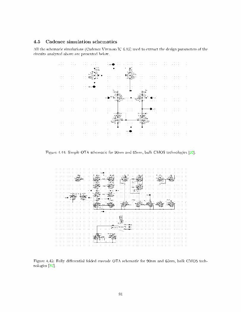
4.5 Cadence simulation schematics
All the schematic simulations (Cadence Virtuoso IC 6.15) used to extract the design parameters of thecircuits analyzed above are presented below.
Figure 4.44: Simple OTA schematic for 90nm and 65nm, bulk CMOS technologies [37].
Figure 4.45: Fully dierential folded coscode OTA schematic for 90nm and 65nm, bulk CMOS tech-nologies [37].
91

Figure 4.46: Ideal Common Mode Feedback Circuit (CMFB) schematic for 90nm and 65nm, bulkCMOS technologies [37].
a) b)
Figure 4.47: AC analysis schematics of (a) simple OTA and (b) fully dierential folded coscode OTAfor 90nm and 65nm, bulk CMOS technologies [37].
a) b)
Figure 4.48: Input CMR schematics of (a) simple OTA and (b) fully dierential folded coscode OTAfor 90nm and 65nm, bulk CMOS technologies [37].
92

a) b)
Figure 4.49: Output voltage range schematics of (a) simple OTA and (b) fully dierential foldedcoscode OTA for 90nm and 65nm, bulk CMOS technologies [37].
a) b)
Figure 4.50: Transient analysis schematics of (a) simple OTA and (b) fully dierential folded coscodeOTA for 90nm and 65nm, bulk CMOS technologies [37].
Figure 4.51: Noise analysis schematic of fully dierential folded coscode OTA for 90nm and 65nm,bulk CMOS technologies [37].
93

Figure 4.52: Input oset voltage schematic of fully dierential folded coscode OTA for 90nm and 65nm,bulk CMOS technologies [37].
94

A Appendix
A.1 Matlab codes
The simple OTA was sized step-by-step, for our convenience we have used matlab code in order tocalculate the basic equations in the proposed order as in the theoretical section above, for both 65nm,90nm bulk cmos technologies.
%%%%% THESIS SIMPLE OTA SIZING -90nm -25dB %%%%%%
clc ;
clear all;
close all;
%%%% Physical constants
k=1.38*10^( -23); % Boltzmann constant
q=1.602*10^( -19); % Coulomb 's constant
Tc=27; % Temperature (C)
Tk =273.15+ Tc; % Temperature (K)
%%%% Normalization quantities
Ut=(k*Tk)/q; % Thermal voltage
%%%% Specifications
sr =100*10^6; % Slew Rate
cl =100*10^( -15); % Load Capacitance
GBW =150*10^6; % Gain Bandwith
AV0 =25; % Open -loop gain given >25db
%%%% Technology parameters
nn =1.24; % Technology Parameter n (slope factor) for nmos
transistor
np =1.22; % Technology Parameter n (slope factor) for pmos
transistor
Kpn =306*10^( -6); % Normalized trasconductance Kpn for nmos
transistor
Kpp =102.9*10^( -6); % Normalized trasconductance Kpp for pmos
transistor
Uan =8.057*10^6; % Early Voltage for nmos transistor
Uap =8.049*10^6; % Early Voltage for pmos transistor
Lmin =90*10^( -9); % Technology L minimum value
%%%% OTA sizing
% Bias (Pmos)
IF5=1; % Moderate inversion
IF4=IF5;
L5=2* Lmin; % Increase the speed (bigger Ft)
95

L6=L5;
IBias=sr*cl;
Io=IBias;
W5=(Io*L5)/(2*np*(Ut^2)*Kpp*IF5); % Solved for w5 the equation IF=
IDsat /(2*n*ut^2*Kp*(W5/L5) as IF5 we assume 1--> WI and IDsat=Io=
IBias
W6=W5;
% Differential pair (Pmos)
gm2overid2 =4*((pi*GBW)/sr); %% gm2/id2 *2=2*pi*GBW/sr
% we create these 2 methods in order to take a very good aproximate
value
% of IF2 in a range of values of IF2
% flag =0;
% IF2 =0.001;
% gm2overid2 =0;
% while flag ~=1;
% gm2overid2 =(1/( np*Ut))*(1/(0.5+ sqrt(IF2 +0.25)));
% if gm2overid2 ==18.84;
% flag =1;
% end
% IF2 =0.001+0.001;
% end
% IF2;
% IF2 =0.0001:0.0001:1;
% gm2overid2 =(1/( np*Ut))*(1/(0.5+ sqrt(IF2 +0.25)));
% plot(IF2 ,gm2overid2);
% IF2 =0.913;
% gm2overid2 =(1/( np*Ut))*(1/(0.5+ sqrt(IF2 +0.25)));
%
% IF2_TABLE =[0.1 0.2 0.3 0.4 0.5 0.6 0.7 0.8 0.9 1 3 5 7 9 11 20 40 60
80 100]
% for i=1:20
% gm2overid2(i)=(1/(np*Ut))*(1/(0.5+ sqrt(IF2_TABLE(i)+0.25)))
% end
% range_values =(0.1:0.1:100);
% IF2=interp1q(IF2_TABLE (9),gm2overid2 (9),range_values)
% IF2
% The best approximation methot in order to find the IF2 is to use
Linear
% interpolation
% IF2_TABLE =[0.0001 0.001 0.01 0.1 0.2 0.3 0.4 0.5 0.6 0.7 0.8 0.9 1
1.1 1.2 1.3 1.4 1.5 2 2.5 3 3.5 4 4.5 5 7 9 11 20 40 60 80 100 120
140]
% for i=1:35
% gm2overid2(i)=(1/(np*Ut))*(1/(0.5+ sqrt(IF2_TABLE(i)+0.25)))
% end
96

%
%
% IF2 =1.1
%
% for i=1.1:0.001:1.2
% gm2overid2_aprox =18.6027+(i -1.1) *((19.0758 -18.6027) /(1.2 -1.1))
% if gm2overid2_aprox ==18.84
% IF2
% end
% IF2=IF2 +0.001
% end
% plot (IF2_TABLE ,gm2overid2 ,'-o',IF2 ,gm2overid2_aprox);
% title ('gm2/id2 plot to IF2 ');
% xlabel ('IF2 [-]');
% ylabel ('gm2/id2 [1/V]');
% legend ('gm2/id2 =(1/( np*Ut))*(1/(0.5+ sqrt(IF2 +0.25)))','location ','
southwest ');
% set (gca ,'XScale ','log ')
% hold on;
% grid on;
IF2 =1.15;
gm2overid2 =(1/(np*Ut))*(1/(0.5+ sqrt(IF2 +0.25)));
Id2=Io/2;
W2overL2=Id2/(IF2 *2*np*(Ut^2)*Kpp); % We compute W2overL2 from this
equation where we put as IDsat=I0/2 and IF2 with above value 0.931
AV =10^( AV0 /20); % To convert dB the open -loop gain parameter given
>25db in specifications ,approximate this in order to achieve the
correct W2 & L2
% Ispec2 =2*n*(Ut^2)*Kpp*W2overL2; % It is computed by the expression
IF2=Id2/Ispec
% Id2=IF2*Ispec2; % It is computed by the expression IF2=Id2/Ispec
gm2=gm2overid2*Id2;
Rout2=AV/gm2; % It is computed by AV0=gm2*Rout
gds2 =2/ Rout2; % Given
L2=Id2/(gds2*Uap); % It is computed by gds=IDsat /(2* Uap)
L2=L2*4; % In order to achive gm in op 's cadence
L1=L2;
W2=W2overL2*L2;
W1=W2;
% L=AV/( gm2overid2*Uap) % This computes the L od all the differential
pair
% Active Load (nmos)
% The best approximation methot in order to find the IF4 is to use
Linear
% interpolation
% IF4_TABLE =[0.0001 0.001 0.01 0.1 0.2 0.3 0.4 0.5 0.6 0.7 0.8 0.9 1
1.1 1.2 1.3 1.4 1.5 2 2.5 3 3.5 4 4.5 5 5.5 6 6.5 7 7.5 8 9 11 20
40 60 80 100 120 140]
97

% for i=1:40
% gm4overid4(i)=(1/(nn*Ut))*(1/(0.5+ sqrt(IF4_TABLE(i)+0.25)))
% end
%
%
% IF4 =7.5
%
% for i=7.5:0.001:8
% gm4overid4_aprox =9.2491+(i -7.5) *((9.4981 -9.2491) /(8 -7.5))
% if gm4overid4_aprox ==9.42
% IF4
% end
% IF4=IF4 +0.001
% end
% plot (IF4_TABLE ,gm4overid4 ,'-o',IF4 ,gm4overid4_aprox);
% title ('gm4/id4 plot to IF4 ');
% xlabel ('IF4 [-]');
% ylabel ('gm4/id4 [1/V]');
% legend ('gm4/id4 =(1/( nn*Ut))*(1/(0.5+ sqrt(IF4 +0.25)))','location ','
southwest ');
% set (gca ,'XScale ','log ')
% hold on;
% grid on;
IF4 =7.65;
Id4=Id2;
% gm4overid4 =(1/( nn*Ut))*(1/(0.5+ sqrt(IF4 +0.25)));
gm4overid4 =0.5* gm2overid2; % In order to minimize the noise
contribution
W4overL4=Id4/(IF4 *2*nn*(Ut^2)*Kpn); % we compute W2overL2 from this
equation where we put as IDsat=I0/2 and IF4 with above value 7.5
% Ispec4 =2*n*(Ut^2)*Kpn*W4overL4; % It is computed by the expression
IF4=Id4/Ispec
% Id4=IF4*Ispec4; % It is computed by the expression IF4=Id4/Ispec
gm4=gm4overid4*Id4;
Rout4=AV/gm4; % It is computed by AV0=gm4*Rout
gds4 =2/ Rout4; % Given
L4=Id4/(gds4*Uan); % It is computed by gds4=IDsat /(2* Uan)
L4=L4*2; % In order to achive gm in op's cadence
L3=L4;
W4=W4overL4*L4;
W3=W4;
% We compute the area of each pair of transistors
A1_2 =2*(L1*W1);
A3_4 =2*(L4*W4);
A5_6 =2*(L5*W5);
% We compute the total OTA Area
A=A1_2+A3_4+A5_6;
98

% % First optimization to reduce the total area
% We change the widths and the lengths of "big" devices (Pmos)
% W1_new =480*(10^( -9));
% W2_new=W1_new;
% W4_new =360*(10^( -9));
% W3_new=W4_new;
% W5_new =9.48*(10^( -6));
% W6_new=W5_new;
% L1_new =75*(10^( -9));
% L2_new=L1_new;
% L4_new =180*(10^( -9));
% L3_new=L4_new;
% L5_new =130*(10^( -9));
% L6_new=L5_new;
%
%
%
% % We re -compute the area of each pair of transistors
%
% A1_2_new =2*( L1_new*W1_new);
% A3_4_new =2*( L4_new*W4_new);
% A5_6_new =2*( L5_new*W5_new);
%
%
% % We re -compute the total OTA Area
%
% A_new=A1_2_new+A3_4_new+A5_6_new;
%
% Second optimization to increase the open loop gain & also to reduce
the
% mismatch
% For the open -loop gain
W1_new_1 =2*W1;
L1_new_1 =2*L1;
W2_new_1=W1_new_1;
L2_new_1=L1_new_1;
W3_new_1 =2*W3;
L3_new_1 =2*L3;
W4_new_1=W3_new_1;
L4_new_1=L3_new_1;
% For the mismatch
W5_new_1 =2*W5;
L5_new_1 =2*L5;
W6_new_1=W5_new_1;
99

L6_new_1=L5_new_1;
% We re -compute the area of each pair of transistors
A1_2_new_1 =2*( L1_new_1*W1_new_1);
A3_4_new_1 =2*( L3_new_1*W3_new_1);
A5_6_new_1 =2*( L5_new_1*W5_new_1);
% We re -compute the total OTA Area
A_new_1=A1_2_new_1+A3_4_new_1+A5_6_new_1;
%%%%% THESIS SIMPLE OTA SIZING -90nm -25dB %%%%%%
clc ;
clear all;
close all;
%%%% Physical constants
k=1.38*10^( -23); % Boltzmann constant
q=1.602*10^( -19); % Coulomb 's constant
Tc=27; % Temperature (C)
Tk =273.15+ Tc; % Temperature (K)
%%%% Normalization quantities
Ut=(k*Tk)/q; % Thermal voltage
%%%% Specifications
sr =100*10^6; % Slew Rate
cl =100*10^( -15); % Load Capacitance
GBW =150*10^6; % Gain Bandwith
AV0 =25; % Open -loop gain given >25db
%%%% Technology parameters
nn =1.24; % Technology Parameter n (slope factor) for nmos
transistor
np =1.22; % Technology Parameter n (slope factor) for pmos
transistor
Kpn =306*10^( -6); % Normalized trasconductance Kpn for nmos
transistor
Kpp =102.9*10^( -6); % Normalized trasconductance Kpp for pmos
transistor
Uan =8.057*10^6; % Early Voltage for nmos transistor
Uap =8.049*10^6; % Early Voltage for pmos transistor
Lmin =90*10^( -9); % Technology L minimum value
%%%% OTA sizing
100

% Bias (Pmos)
IF5=1; % Moderate inversion
IF4=IF5;
L5=2* Lmin; % Increase the speed (bigger Ft)
L6=L5;
IBias=sr*cl;
Io=IBias;
W5=(Io*L5)/(2*np*(Ut^2)*Kpp*IF5); % Solved for w5 the equation IF=
IDsat /(2*n*ut^2*Kp*(W5/L5) as IF5 we assume 1--> WI and IDsat=Io=
IBias
W6=W5;
% Differential pair (Pmos)
gm2overid2 =4*((pi*GBW)/sr); %% gm2/id2 *2=2*pi*GBW/sr
% we create these 2 methods in order to take a very good aproximate
value
% of IF2 in a range of values of IF2
% flag =0;
% IF2 =0.001;
% gm2overid2 =0;
% while flag ~=1;
% gm2overid2 =(1/( np*Ut))*(1/(0.5+ sqrt(IF2 +0.25)));
% if gm2overid2 ==18.84;
% flag =1;
% end
% IF2 =0.001+0.001;
% end
% IF2;
% IF2 =0.0001:0.0001:1;
% gm2overid2 =(1/( np*Ut))*(1/(0.5+ sqrt(IF2 +0.25)));
% plot(IF2 ,gm2overid2);
% IF2 =0.913;
% gm2overid2 =(1/( np*Ut))*(1/(0.5+ sqrt(IF2 +0.25)));
%
% IF2_TABLE =[0.1 0.2 0.3 0.4 0.5 0.6 0.7 0.8 0.9 1 3 5 7 9 11 20 40 60
80 100]
% for i=1:20
% gm2overid2(i)=(1/(np*Ut))*(1/(0.5+ sqrt(IF2_TABLE(i)+0.25)))
% end
% range_values =(0.1:0.1:100);
% IF2=interp1q(IF2_TABLE (9),gm2overid2 (9),range_values)
% IF2
% The best approximation methot in order to find the IF2 is to use
Linear
% interpolation
% IF2_TABLE =[0.0001 0.001 0.01 0.1 0.2 0.3 0.4 0.5 0.6 0.7 0.8 0.9 1
101

1.1 1.2 1.3 1.4 1.5 2 2.5 3 3.5 4 4.5 5 7 9 11 20 40 60 80 100 120
140]
% for i=1:35
% gm2overid2(i)=(1/(np*Ut))*(1/(0.5+ sqrt(IF2_TABLE(i)+0.25)))
% end
%
%
% IF2 =1.1
%
% for i=1.1:0.001:1.2
% gm2overid2_aprox =18.6027+(i -1.1) *((19.0758 -18.6027) /(1.2 -1.1))
% if gm2overid2_aprox ==18.84
% IF2
% end
% IF2=IF2 +0.001
% end
% plot (IF2_TABLE ,gm2overid2 ,'-o',IF2 ,gm2overid2_aprox);
% title ('gm2/id2 plot to IF2 ');
% xlabel ('IF2 [-]');
% ylabel ('gm2/id2 [1/V]');
% legend ('gm2/id2 =(1/( np*Ut))*(1/(0.5+ sqrt(IF2 +0.25)))','location ','
southwest ');
% set (gca ,'XScale ','log ')
% hold on;
% grid on;
IF2 =1.15;
gm2overid2 =(1/(np*Ut))*(1/(0.5+ sqrt(IF2 +0.25)));
Id2=Io/2;
W2overL2=Id2/(IF2 *2*np*(Ut^2)*Kpp); % We compute W2overL2 from this
equation where we put as IDsat=I0/2 and IF2 with above value 0.931
AV =10^( AV0 /20); % To convert dB the open -loop gain parameter given
>25db in specifications ,approximate this in order to achieve the
correct W2 & L2
% Ispec2 =2*n*(Ut^2)*Kpp*W2overL2; % It is computed by the expression
IF2=Id2/Ispec
% Id2=IF2*Ispec2; % It is computed by the expression IF2=Id2/Ispec
gm2=gm2overid2*Id2;
Rout2=AV/gm2; % It is computed by AV0=gm2*Rout
gds2 =2/ Rout2; % Given
L2=Id2/(gds2*Uap); % It is computed by gds=IDsat /(2* Uap)
L2=L2*4; % In order to achive gm in op 's cadence
L1=L2;
W2=W2overL2*L2;
W1=W2;
% L=AV/( gm2overid2*Uap) % This computes the L od all the differential
pair
% Active Load (nmos)
% The best approximation methot in order to find the IF4 is to use
Linear
102

% interpolation
% IF4_TABLE =[0.0001 0.001 0.01 0.1 0.2 0.3 0.4 0.5 0.6 0.7 0.8 0.9 1
1.1 1.2 1.3 1.4 1.5 2 2.5 3 3.5 4 4.5 5 5.5 6 6.5 7 7.5 8 9 11 20
40 60 80 100 120 140]
% for i=1:40
% gm4overid4(i)=(1/(nn*Ut))*(1/(0.5+ sqrt(IF4_TABLE(i)+0.25)))
% end
%
%
% IF4 =7.5
%
% for i=7.5:0.001:8
% gm4overid4_aprox =9.2491+(i -7.5) *((9.4981 -9.2491) /(8 -7.5))
% if gm4overid4_aprox ==9.42
% IF4
% end
% IF4=IF4 +0.001
% end
% plot (IF4_TABLE ,gm4overid4 ,'-o',IF4 ,gm4overid4_aprox);
% title ('gm4/id4 plot to IF4 ');
% xlabel ('IF4 [-]');
% ylabel ('gm4/id4 [1/V]');
% legend ('gm4/id4 =(1/( nn*Ut))*(1/(0.5+ sqrt(IF4 +0.25)))','location ','
southwest ');
% set (gca ,'XScale ','log ')
% hold on;
% grid on;
IF4 =7.65;
Id4=Id2;
% gm4overid4 =(1/( nn*Ut))*(1/(0.5+ sqrt(IF4 +0.25)));
gm4overid4 =0.5* gm2overid2; % In order to minimize the noise
contribution
W4overL4=Id4/(IF4 *2*nn*(Ut^2)*Kpn); % we compute W2overL2 from this
equation where we put as IDsat=I0/2 and IF4 with above value 7.5
% Ispec4 =2*n*(Ut^2)*Kpn*W4overL4; % It is computed by the expression
IF4=Id4/Ispec
% Id4=IF4*Ispec4; % It is computed by the expression IF4=Id4/Ispec
gm4=gm4overid4*Id4;
Rout4=AV/gm4; % It is computed by AV0=gm4*Rout
gds4 =2/ Rout4; % Given
L4=Id4/(gds4*Uan); % It is computed by gds4=IDsat /(2* Uan)
L4=L4*2; % In order to achive gm in op's cadence
L3=L4;
W4=W4overL4*L4;
W3=W4;
% We compute the area of each pair of transistors
A1_2 =2*(L1*W1);
A3_4 =2*(L4*W4);
A5_6 =2*(L5*W5);
103

% We compute the total OTA Area
A=A1_2+A3_4+A5_6;
% % First optimization to reduce the total area
% We change the widths and the lengths of "big" devices (Pmos)
% W1_new =480*(10^( -9));
% W2_new=W1_new;
% W4_new =360*(10^( -9));
% W3_new=W4_new;
% W5_new =9.48*(10^( -6));
% W6_new=W5_new;
% L1_new =75*(10^( -9));
% L2_new=L1_new;
% L4_new =180*(10^( -9));
% L3_new=L4_new;
% L5_new =130*(10^( -9));
% L6_new=L5_new;
%
%
%
% % We re -compute the area of each pair of transistors
%
% A1_2_new =2*( L1_new*W1_new);
% A3_4_new =2*( L4_new*W4_new);
% A5_6_new =2*( L5_new*W5_new);
%
%
% % We re -compute the total OTA Area
%
% A_new=A1_2_new+A3_4_new+A5_6_new;
%
% Second optimization to increase the open loop gain & also to reduce
the
% mismatch
% For the open -loop gain
W1_new_1 =2*W1;
L1_new_1 =2*L1;
W2_new_1=W1_new_1;
L2_new_1=L1_new_1;
W3_new_1 =2*W3;
L3_new_1 =2*L3;
W4_new_1=W3_new_1;
L4_new_1=L3_new_1;
104

% For the mismatch
W5_new_1 =2*W5;
L5_new_1 =2*L5;
W6_new_1=W5_new_1;
L6_new_1=L5_new_1;
% We re -compute the area of each pair of transistors
A1_2_new_1 =2*( L1_new_1*W1_new_1);
A3_4_new_1 =2*( L3_new_1*W3_new_1);
A5_6_new_1 =2*( L5_new_1*W5_new_1);
% We re -compute the total OTA Area
A_new_1=A1_2_new_1+A3_4_new_1+A5_6_new_1;
Here there are demonstrated the Matlab Figures of gmId vs. IC used in order to compute IC,2and IC,4in simple OTA in both 90nm and 65nm PDKs,
a) b)
c) d)
Figure A.1: Simulated transconductance-to-current-ratio gmID
vs. inversion coecient IC used to com-pute IC,2 and IC,4 for (a), (c) 90nm and (b), (d) 65nm, bulk CMOS process.
In the same way, we have used the following matlab codes in order to size the fully dierentialfolded cascode (FDFC) OTA also,
105

%%%% THESIS FULLY DIFFERENTIAL FOLDED CASCODE OTA SIZING -90nm -50dB
%%%%
clc ;
clear all;
close all;
%%%% Physical constants
k=1.38*10^( -23);
q=1.602*10^( -19);
Tc=27;
Tk =273.15+ Tc;
%%%% Normalization quantities
Ut=(k*Tk)/q;
%%%% Specifications of the circuit
GBW =150*(10^6); % Gain Bandwith
sr =100*(10^6); % Slew Rate
cl =100*(10^( -15)); % Load Capacitance
nn =1.24; % Technology Parameter nn (nmos transistors)
np =1.22; % Technology Parameter np (pmos transistors)
Kpp =102.9*10^( -6); % Normalized trasconductance Kpp for pmos
transistor
Kpn =306*10^( -6); % Normalized trasconductance Kpn for nmos
transistor
Uap =8.049*10^6; % Early Voltage for pmos transistor
Uan =8.057*10^6; % Early Voltage for nmos transistor
%%%% Sizing of OTA
%%%% Bias current -Differential pair
% Calculation of currents I0 and I1 and also we determine the
transconductance ,the inversion factor ,and the W1/L1 ratio of the
differential pair
% Calculate the Bias currents I0 and I1 in order to achieve the
specified slew rate
I0=sr*cl;
I1=I0/2;
gm1=2*pi*cl*GBW; % We calculate the transconductance gm1
Id1=I0/2;
gm1overid1=gm1/Id1; % We can calculate the gm1 over id1 value so we
can find with linear interpolation method the IF1 value
% The best approximation method in order to find the IF1 is to use
Linear
% interpolation
106

% IF1_TABLE =[0.0001 0.001 0.01 0.1 0.2 0.3 0.4 0.5 0.6 0.7 0.8 0.9
0.95 1 1.1 1.2 1.3 1.4 1.5 2 3 5 7 9 11 20 40 60 80 100]
% for i=1:30
% gm1overid1(i)=(1/(np*Ut))*(1/(0.5+ sqrt(IF1_TABLE(i)+0.25)))
% end
%
% IF1 =1.1
%
% for i=1.1:0.001:1.2
% gm1overid1_aprox =18.6027+(i -1.1) *((19.0758 -18.6027) /(1.2 -1.1))
% if gm1overid1_aprox ==18.8496
% IF1
% end
% IF1=IF1 +0.001
% end
% plot (IF1_TABLE ,gm1overid1 ,'-o',IF1 ,gm1overid1_aprox);
% title ('gm1/id1 plot to IF1 ');
% xlabel ('IF1 (-) ');
% ylabel ('gm1/id1 (1/V)');
% legend ('gm1/id1 =(1/( np*Ut))*(1/(0.5+ sqrt(IF1 +0.25)))','location ','
southwest ');
% set (gca ,'XScale ','log ')
% hold on;
% grid on;
IF1 =1.15;
% gm1overid1 =(1/( np*Ut))*(1/(0.5+ sqrt(IF1 +0.25))) % best approximation
of IF1 is 1.15
W1overL1=Id1/(IF1 *2*np*(Ut^2)*Kpp); % We compute the W1/L1 ratio
%%%% Folded cascoded current mirrors
% We calculate the W/L of the 8 transistor composing the folded
cascode stage
% We choose moderate inversion for transistors m5-m6,m7-m8 ,m9 -m10 to
keep the saturation voltage small and also to have small area
consumption
% We choose strong inversion for transistors m3-m4 to reduce noise
contribution
IF9=1;
IF7=1;
IF5=1;
IF10=IF9;
IF8=IF7;
IF6=IF5;
Id9=I1;
Id7=I1;
Id5=I1;
% Same current mirror
107

Id10=Id9;
Id8=Id7;
Id6=Id5;
W9overL9=Id9/(IF9 *2*np*(Ut^2)*Kpp); % Pmos current mirror
W7overL7=Id7/(IF7 *2*np*(Ut^2)*Kpp); % Pmos current mirror
W5overL5=Id5/(IF5 *2*nn*(Ut^2)*Kpn); % Nmos current mirror
% Same W/L ratio in the same current mirrors
W10overL10=W9overL9;
W8overL8=W7overL7;
W6overL6=W5overL5;
% We choose strong inversion for these transistors
IF3 =10;
IF4=IF3;
I2=(I0/2)+I1;
Id3=I2;
% Same current mirror
Id4=Id3;
W3overL3=Id3/(IF3 *2*nn*(Ut^2)*Kpn); % Nmos current mirror
% same W/L ratio in the same current mirrors
W4overL4=W3overL3;
% Here we calculate the output resistance
A0=50; % Open -loop gain >50 dB
AV =10^(A0/20);
Rout=AV/gm1;
% Negleting the conductance of the differential pair we compute the
gm5=gm7
gm5 =(1/(np*Ut))*(Id5 /(0.5+ sqrt(IF5 +0.25)));
gm7=gm5;
% As we can choose gds5=gds7 ,gds3=gds9 ,Id3 =2*Id9 ,Id5=Id7 ,L7=L9,L5=2*L3
and Uan almost equal to Uap we can compute the following
Rup=2* Rout;
Rdown=Rup;
L7multL9 =(Rup*Id7*Id9)/(gm7*(Uap^2)); % We solve the equation of Rup
L3multL5 =(Rdown*Id3*Id5)/(gm5*(Uan^2)); % We solve the equation of
Rdown
L7=sqrt(L7multL9);
L9=L7;;
L3=sqrt (2* L3multL5); % We know that L3=2*L9 and L5=L7
108

L5=L3/2;
% They are the same transistors
L10=L9;
L8=L7;
L6=L5;
L4=L3;
% We can calculate the width of all cascode transistors
W9=(Id9*L9)/(2*np*(Ut^2)*Kpp*IF9); % solved for W9 the equation IF=
IDsat /(2*np*ut^2* Kpp*(W9/L9)
W7=(Id7*L7)/(2*np*(Ut^2)*Kpp*IF7); % solved for W7 the equation IF=
IDsat /(2*np*ut^2* Kpp*(W7/L7)
W5=(Id5*L5)/(2*nn*(Ut^2)*Kpn*IF5); % solved for W5 the equation IF=
IDsat /(2*nn*ut^2* Kpn*(W5/L5)
W3=(Id3*L3)/(2*nn*(Ut^2)*Kpn*IF3); % solved for W3 the equation IF=
IDsat /(2*nn*ut^2* Kpp*(W3/L3)
% They are the same transistors
W10=W9;
W8=W7;
W6=W5;
W4=W3;
%%%% Find the length and the width of the differential pair and
current source
% We choose a small L1=200nm
L1 =200*10^( -9);
W1=L1*W1overL1;
W2=W1;
L2=L1;
% To determine LB1 and WB1 we know that IF9=IFB1 and I1=I0/2 and if we
do
% the maths we end up to this
WB1=2*W9;
LB1=L9;
%%%% Design verification & Performance simulation (sizing of
transistors m20 ,m21)
IF20 =1; % we choose moderate inversion as in the other pmos
transistors
IF21=IF20;
L20=LB1; % We choose a L~=162.5 nm as in the other bias Pmos transistor
L21=L20;
Id20=I1; % Id20=I1 =5*10^( -6)
109

Id21=Id20;
W20=(Id20*L20)/(2*np*(Ut^2)*Kpp*IF20);
W21=W20;
% Sizing of the transistor m11 of the cmfb
L11=L3;
IF11=IF3;
Id11=I1; % Id11=I1 =5*10^( -6)
W11=(Id11*L11)/(2*nn*(Ut^2)*Kpn*IF11);
%%%% We compute the area of whole circuit
% We compute the area of each mirror
A3_4 =2*(L3*W3);
A5_6 =2*(L5*W5);
A7_8 =2*(L7*W7);
A9_10 =2*(L9*W9);
% We compute the total cascode area
A=A3_4+A5_6+A7_8+A9_10;
% We compute the area of the bias transistor
A_B1=(LB1*WB1);
% We compute the area of the input differential pair
A1_2 =2*(L1*W1);
% We compute the total FC_OTA area
A_Total=A_B1+A1_2+A3_4+A5_6+A7_8+A9_10;
% Optimazation to achieve Av=50 dB
% In order to optimize we double the size of transistors m3 ,m4 ,m11 ,m1,
m2
L1_new =2*L1;
L2_new =2*L2;
W1_new =2*W1;
W2_new =2*W2;
L3_new =2*L3;
L4_new =2*L4;
W3_new =2*W3;
W4_new =2*W4;
L11_new =2*L11;
W11_new =2*W11;
% We re -compute the area of whole circuit
AB1_new =(LB1*WB1);
A1_2_new =2*( L1_new*W1_new);
110

A3_4_new =2*( L3_new*W3_new);
A5_6_new =2*(L5*W5);
A7_8_new =2*(L7*W7);
A9_10_new =2*(L9*W9);
A_new=A3_4_new+A5_6_new+A7_8_new+A9_10_new+A1_2_new+AB1_new;
%%%% THESIS FULLY DIFFERENTIAL FOLDED CASCODE OTA SIZING -65nm -50dB
%%%%
clc ;
clear all;
close all;
%%%% Physical constants
k=1.38*10^( -23);
q=1.602*10^( -19);
Tc=27;
Tk =273.15+ Tc;
%%%% Normalization quantities
Ut=(k*Tk)/q;
%%%% Specifications of the circuit
GBW =150*(10^6); % Gain Bandwith
sr =100*(10^6); % Slew Rate
cl =100*(10^( -15)); % Load Capacitance
nn =1.25; % Technology Parameter nn (nmos transistors)
np =1.24; % Technology Parameter np (pmos transistors)
Kpp =102*10^( -6); % Normalized trasconductance Kpp for pmos
transistor
Kpn =252*10^( -6); % Normalized trasconductance Kpn for nmos
transistor
Uap =12.53*10^6; % Early Voltage for pmos transistor
Uan =10.37*10^6; % Early Voltage for nmos transistor
%%%% Sizing of OTA
%%%% Bias current -Differential pair
% Calculation of currents I0 and I1 and also we determine the
transconductance ,the inversion factor ,and the W1/L1 ratio of the
differential pair
% Calculate the Bias currents I0 and I1 in order to achieve the
specified slew rate
I0=sr*cl;
I1=I0/2;
gm1=2*pi*cl*GBW; % We calculate the transconductance gm1
111

Id1=I0/2;
gm1overid1=gm1/Id1; % We can calculate the gm1 over id1 value so we
can find with linear interpolation method the IF1 value
% The best approximation method in order to find the IF1 is to use
Linear
% interpolation
% IF1_TABLE =[0.0001 0.001 0.01 0.1 0.2 0.3 0.4 0.5 0.6 0.7 0.8 0.85
0.9 0.95 1.05 1.1 1.15 1.2 1.25 1.3 1.35 1.4 1.45 1.5 2 3 5 7 9 11
20 40 60 80 100]
% for i=1:35
% gm1overid1(i)=(1/(np*Ut))*(1/(0.5+ sqrt(IF1_TABLE(i)+0.25)))
% end
%
% IF1 =1.05
%
% for i=1.05:0.001:1.1
% gm1overid1_aprox =18.7681+(i -1.05) *((19.0166 -18.7681) /(1.1 -1.05))
% if gm1overid1_aprox ==18.8496
% IF1
% end
% IF1=IF1 +0.001
% end
% plot (IF1_TABLE ,gm1overid1 ,'-o',IF1 ,gm1overid1_aprox);
% title ('gm1/id1 plot to IF1 ');
% xlabel ('IF1 (-) ');
% ylabel ('gm1/id1 (1/V)');
% legend ('gm1/id1 =(1/( np*Ut))*(1/(0.5+ sqrt(IF1 +0.25)))','location ','
southwest ');
% set (gca ,'XScale ','log ')
% hold on;
% grid on;
IF1 =1.08;
% gm1overid1 =(1/( np*Ut))*(1/(0.5+ sqrt(IF1 +0.25))) % best approximation
of IF1 is 1.08
W1overL1=Id1/(IF1 *2*np*(Ut^2)*Kpp); % we compute the W1/L1 ratio
%%%% Folded cascoded current mirrors
% We calculate the W/L of the 8 transistor composing the folded
cascode stage
% We choose moderate inversion for transistors m5-m6,m7-m8 ,m9 -m10 to
keep the saturation voltage small and also to have small area
consumption
% We choose strong inversion for transistors m3-m4 to reduce noise
contribution
IF9=1;
IF7=1;
IF5=1;
112

IF10=IF9;
IF8=IF7;
IF6=IF5;
Id9=I1;
Id7=I1;
Id5=I1;
% Same current mirror
Id10=Id9;
Id8=Id7;
Id6=Id5;
W9overL9=Id9/(IF9 *2*np*(Ut^2)*Kpp); % Pmos current mirror
W7overL7=Id7/(IF7 *2*np*(Ut^2)*Kpp); % Pmos current mirror
W5overL5=Id5/(IF5 *2*nn*(Ut^2)*Kpn); % Nmos current mirror
% Same W/L ratio in the same current mirrors
W10overL10=W9overL9;
W8overL8=W7overL7;
W6overL6=W5overL5;
% We choose strong inversion for these transistors
IF3 =10;
IF4=IF3;
I2=(I0/2)+I1;
Id3=I2;
% Same current mirror
Id4=Id3;
W3overL3=Id3/(IF3 *2*nn*(Ut^2)*Kpn); % Nmos current mirror
% same W/L ratio in the same current mirrors
W4overL4=W3overL3;
% Here we calculate the output resistance
A0=50; % Open -loop gain >50 dB
AV =10^(A0/20);
Rout=AV/gm1;
% Negleting the conductance of the differential pair we compute the
gm5=gm7
gm5 =(1/(np*Ut))*(Id5 /(0.5+ sqrt(IF5 +0.25)));
gm7=gm5;
% As we can choose gds5=gds7 ,gds3=gds9 ,Id3 =2*Id9 ,Id5=Id7 ,L7=L9,L5=2*L3
and Uan almost equal to Uap we can compute the following
Rup=2* Rout;
113

Rdown=Rup;
L7multL9 =(Rup*Id7*Id9)/(gm7*(Uap^2)); % we solve the equation of Rup
L3multL5 =(Rdown*Id3*Id5)/(gm5*(Uan^2)); % we solve the equation of
Rdown
L7=sqrt(L7multL9);
L9=L7;
L3=sqrt (2* L3multL5); % we know that L3 =2.4*L9 and L5 =1.2*L7 so , L3=2*
L5
L5=L3/2;
% They are the same transistors
L10=L9;
L8=L7;
L6=L5;
L4=L3;
% We can calculate the width of all cascode transistors
W9=(Id9*L9)/(2*np*(Ut^2)*Kpp*IF9); % solved for W9 the equation IF=
IDsat /(2*np*ut^2* Kpp*(W9/L9)
W7=(Id7*L7)/(2*np*(Ut^2)*Kpp*IF7); % solved for W7 the equation IF=
IDsat /(2*np*ut^2* Kpp*(W7/L7)
W5=(Id5*L5)/(2*nn*(Ut^2)*Kpn*IF5); % solved for W5 the equation IF=
IDsat /(2*nn*ut^2* Kpn*(W5/L5)
W3=(Id3*L3)/(2*nn*(Ut^2)*Kpn*IF3); % solved for W3 the equation IF=
IDsat /(2*nn*ut^2* Kpp*(W3/L3)
% They are the same transistors
W10=W9;
W8=W7;
W6=W5;
W4=W3;
%%%% Find the length and the width of the differential pair and
current source
% We choose a small L1=150nm
L1 =150*10^( -9);
W1=L1*W1overL1;
W2=W1;
L2=L1;
% To determine LB1 and WB1 we know that IF9=IFB1 and I1=I0/2 and if we
do
% the maths we end up to this
WB1=2*W9;
LB1=L9;
114
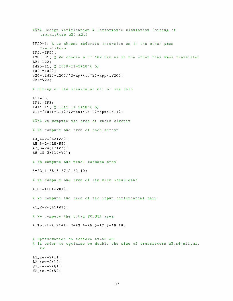
%%%% Design verification & Performance simulation (sizing of
transistors m20 ,m21)
IF20 =1; % we choose moderate inversion as in the other pmos
transistors
IF21=IF20;
L20=LB1; % We choose a L~=162.5 nm as in the other bias Pmos transistor
L21=L20;
Id20=I1; % Id20=I1 =5*10^( -6)
Id21=Id20;
W20=(Id20*L20)/(2*np*(Ut^2)*Kpp*IF20);
W21=W20;
% Sizing of the transistor m11 of the cmfb
L11=L3;
IF11=IF3;
Id11=I1; % Id11=I1 =5*10^( -6)
W11=(Id11*L11)/(2*nn*(Ut^2)*Kpn*IF11);
%%%% We compute the area of whole circuit
% We compute the area of each mirror
A3_4 =2*(L3*W3);
A5_6 =2*(L5*W5);
A7_8 =2*(L7*W7);
A9_10 =2*(L9*W9);
% We compute the total cascode area
A=A3_4+A5_6+A7_8+A9_10;
% We compute the area of the bias transistor
A_B1=(LB1*WB1);
% We compute the area of the input differential pair
A1_2 =2*(L1*W1);
% We compute the total FC_OTA area
A_Total=A_B1+A1_2+A3_4+A5_6+A7_8+A9_10;
% Optimazation to achieve Av=50 dB
% In order to optimize we double the size of transistors m3 ,m4 ,m11 ,m1,
m2
L1_new =2*L1;
L2_new =2*L2;
W1_new =2*W1;
W2_new =2*W2;
115

L3_new =2*L3;
L4_new =2*L4;
W3_new =2*W3;
W4_new =2*W4;
L11_new =2*L11;
W11_new =2*W11;
% We re -compute the area of whole circuit
AB1_new =(LB1*WB1);
A1_2_new =2*( L1_new*W1_new);
A3_4_new =2*( L3_new*W3_new);
A5_6_new =2*(L5*W5);
A7_8_new =2*(L7*W7);
A9_10_new =2*(L9*W9);
A_new=A3_4_new+A5_6_new+A7_8_new+A9_10_new+A1_2_new+AB1_new;
Here there are demonstrated the Matlab Figures of gmId vs. IC used in order to compute IC,1 in FDFCOTA in both 90nm and 65nm PDKs,
a) b)
Figure A.2: Simulated transconductance-to-current-ratio gmID
vs. inversion coecient IC used to com-pute IC,1 for (a) 90nm and (b) 65nm, bulk CMOS process.
116

References
[1] Adel S. Sedra and Kenneth C. Smith, Microelectronics Circuits, Oxford 2009.
[2] Bakshi, U. A. Godse, A. P., Electronic Circuits, Technical Publications 2007.
[3] Christophe Lécuyer, Making Silicon Valley: Innovation and the Growth of High Tech, 1930-1970,MIT Press 2006.
[4] R. Jacob Baker, CMOS Circuit Design, Layout, and Simulation, IEEE Press Series on Microelec-tronic Systems 2010.
[5] Behzad Razavi, Design of Analog Intergrated Circuits, Boston McGraw-Hill 2001.
[6] Carlos Galup-Montoro, Márcio Cherem Schneider, MOSFET modeling for circuit analysis anddesign, World Scientic Publishing Co. Pte. Ltd., 2007.
[7] David M. Binkley, Tradeos and Optimization in Analog CMOS Design, John Wiley 2008.
[8] Dalton Colombo, Christian Fayomi, Frederic Nabki, Luiz F. Ferreira, Gilson Wirth, and SergioBampi A Design Methodology Using the Inversion Coecient for Low-Voltage Low-Power CMOSVoltage References, Journal of Integrated Circuits and Systems, August 2011.
[9] Colin C. McAndrew and Paul A. Layman, MOSFET eective channel length, threshold volt-age, and series resistance determination by robust optimization, IEEE Trans. Electron Devices,October 1992.
[10] E. H. Nicollian & J. R. Brews., MOS, (Metal Oxide Semiconductor) Physics and Technology, JohnWiley & Sons, 1982.
[11] Anne-Johan Annema, Bram Nauta, Ronald van Langevelde & Hans Tuinhout, Analog Circuitsin Ultra-Deep-Submicron CMOS, IEEE JSSC, January 2005.
[12] Sung-Mo Kang & Yusuf Leblebici, CMOS Digital Integrated Circuits: Analysis and Design,McGraw-Hill 2003.
[13] G. Ghibaudo, S. Bruyere, T. Devoivre, DeSalvo & E. Vincent, Improved method for the oxidethickness extraction in MOS structures with ultrathin gate dielectrics, IEEE ICMTS, March 1999.
[14] David A. Johns & Ken Martin, Analog Integrated Circuit Design, John Wiley & Sons Inc. 1997.
[15] E. Vincent, G. Ghibaudo, G. Morin & C. Papadas, On The Oxide Thickness Extraction InDeep-Submicron Technologies, IEEE ICMTS, 1997.
[16] Matthias Bucher, Wladek Grabinski,EKV MOS Transistor Modelling & RF Application, pp. 20,1999.
[17] A. Bazigos, M. Bucher, J. Assenmacher, S. Decker, W. Grabinski, Y. Papananos, An AdjustedConstant-Current Method to Determine Saturated and Linear Mode Threshold Voltage of MOS-FETs , IEEE Trans. Electron Devices, vol. 58, nr. 11, pp. 3751-3758, Nov. 2011.
[18] MOSFET modeling & BSIM3 user's guide, chapter 3, threshold voltage model, pp. 68-71.
[19] Wladyslaw Grabinski, Matthias Bucher, François Krummenacher, The EKV Model ParameterExtraction Based on its IC-CAP USERC Implementation, pp.11.
[20] Havard Lund, IV and CV characterization of 90nm CMOS transistors, Master of Science in Elec-tronics, Norwegian University of Science and Technology Department of Electronics and Telecom-munications, June 2006.
[21] Gaubert, Philippe & Teramoto, Akinobu, Carrier Mobility in Field-Eect Transistors, 2017.
117

[22] F. Stern, Calculated Temperature Dependence of Mobility in Silicon Inversion Layers, PhysicalReview Letters, vol. 44, no. 22, pp. 14691472, 1980.
[23] A.M. Sonnet, R.V. Galatage, P.K. Hurley, E. Pelucchi, K. Thomas, A. Gocalinska, J. Huang, N.Goel, G. Bersuker, W.P. Kirk, C.L. Hinkle, E.M. Vogel, Remote phonon and surface roughnesslimited universal electron mobility of In0.53, Ga0.47 as surface channel MOSFETs, Microelec-tronic Engineering, vol 88, nr. 10, pp. 1083-1086, July 2011.
[24] Loukas Chevas, Aristeidis Nikolaou, Matthias Bucher, Nikos Makris, Alexia Papadopoulou, Apos-tolos Zografos, Giulio Borghello, Henri D. Koch, Federico Faccio, Investigation of Scaling andTemperature Eects in Total Ionizing Dose (TID) Experiments in 65 nm CMOS, 25th Interna-tional Conference (MIXDES), pp. 313-318, june 2018.
[25] C. Enz, F. Chicco, A. Pezzotta, "Nanoscale MOSFET Modeling, Part 1: The simplied EKV modelfor the design of low-power analog circuits", IEEE Solid-State Circuits Magazine, pp. 26-35, Aug.2017.
[26] C. Enz, F. Chicco, A. Pezzotta, "Nanoscale MOSFET Modeling, Part 2: Using the InversionCoecient as the Primary Design Parameter, IEEE Solid-State Circuits Magazine, pp. 73-81,Nov. 2017.
[27] D.M.Binkley, B.J.Blalock, J.M.Rochelle, Optimizing Drain Current, Inversion Level, and Chan-nel Length in Analog CMOS Design, Analog Integrated Circuits and Signal Processing, vol.47,pp. 137-163, May 2006.
[28] Márcio Cherem Schneider, Carlos Galup-Montoro, CMOS Analog Design Using All-Region MOS-FET Modeling, Cambridge University Press, 2010.
[29] Ka Nang Leung and P. K. T. Mok, "Analysis of multistage amplier-frequency compensation",IEEE Transactions on Circuits and Systems I: Fundamental Theory and Applications, vol. 48, no.9, pp. 1041-1056, Sept. 2001.
[30] Christian C.Enz and Eric A. Vittoz, Charge-based MOS Transistor Modeling. The EKV model forlow-power and RF IC design, Jonh Wiley 2006.
[31] H.P. Hsu, Theory and Problems of Signals and Systems, McGraw-Hill 1995.
[32] E.G. Ioannidis, C.A. Dimitriadis, S. Haendler, R.A. Bianchi, J.Jomaah, G. Ghibaudo, Improvedanalysis and modeling of low-frequency noise in nanoscale MOSFETs, Solid State Electronics,vol. 76, pp. 54-59, 2012.
[33] N. Mavredakis, P. Habas, A. Acovic, R. Meyer and M. Bucher, Variability of Low FrequencyNoise in Moderated-Sized MOSFETs-A Model for the Area-and Gate Voltage-Dependence, IEEENoise and Fluctuations (ICNF), International Conference, 2015.
[34] Cijan Gregor & Tuma Tadej, Modeling and simulation of MOS transistor mismatch, 2007.
[35] Alan Hastings, The Art of Analog Layout, Prentice Hall, Upper Saddle River, NJ, 2001.
[36] P. R. Kinget, Device mismatch: an analog design perspective, Proceedings of IEEE ISCAS, pp.12451248, 2007.
[37] IDESA-Implementation of widespread ICDEsign Skills in advanced deep submicron technologiesat European Academia, Course "Advanced Analog Implementation Flow".
[38] Roberto Pereira-Arroyo, Frank Nicaragua-Guzman, Alfonso Chacon-Rodrguez, Design of anOperational Transconductance Amplier applying multiobjective optimization, Proceedings of theArgentine-Uruguay School of Micro-Nanoelectronics, Technology and Applications, 2010.
118

[39] S. Bracho, Amp.operacionales/transconductancia, 2005. [Online]. Available:http://www.teisa.unican.es/teisa/classes/docencia/bracho/1685/AmpOp.pdf.
[40] Y. Tsividis,Mixed Analog-Digital VLSI Devices and Technology, Colombia University, USA: WorldScientic Publishing, 2002.
[41] M. Baru, Analog design methodologies when every nanoampere counts, in CMOS ET WorkshopVancouver, 2009.
[42] Danica Stefanovic, Maher Kayal, Structured Analog CMOS Design, Springer 2008.
[43] P. Allen, D. Holberg, CMOS Analog Circuit Design, Oxford University Press, second edition,January 2002.
[44] Paul R. Gray, Paul J. Hurst, Stephen H. Lewis, Robert G. Meyer, Analysis and Design of AnalogIntegrated Circuits, New York: Wiley, 2001.
[45] Hank Zumbahlen, Linear Circuit Design Handbook, Analog Devices Newnes/Elsevier, 2008.
[46] Cox James, Fundamentals of linear electronics: integrated and discrete, Delmar Thompson Learn-ing, 2002.
[47] M. Holmes, J. Ramirez-Angulo, and R.G. Carvajal, New Architectures of Class AB CMOS andBICMOS Operational Ampliers with Local Common Mode Feedback, Proceedings of the 2002Midwest Symposium on Circuits and Systems, Tulsa, Oklahoma, August 2002.
[48] Michael Leigh Holmes, "Application of Local Common Mode Feedback Techniques to EnhanceSlew Rate and Gain-Bandwidth of CMOS Operational Ampliers", Master of Science in ElectricalEngineering, New Mexico State University, December 2002.
[49] D. Johns and K. Martin, Analog Integrated Circuit Design, New York: John Wiley & Sons, 1 sted., 1997.
[50] J. Ramirez-Angulo and M. Holmes, A Simple Technique to Signicantly Enhance Slew Rate andBandwidth of One-Stage CMOS Operational Ampliers, Proceedings of the 2002 InternationalSymposium on Circuits and Systems, Phoenix, Arizona, May 2002.
[51] Y. Tsividis, Moderate inversion in MOS devices, Solid-State Electronics, vol. 25, pp. 10991104,Nov. 1982.
[52] M. del Mar Hershenson, S. P. Boyd, T. H. Lee, Optimal design of a CMOS op-amp via geometricprogramming, IEEE Transactions on Computer-Aided Design of Integrated Circuits and Systems,pp. :1-21, January 2001.
[53] A. Shameli and P. Heydari, A novel power optimization technique for ultra-low power RFICs,Proceedings of the 2006 International Symposium on Low Power Electronic Design (ISLPED),pp. 274279, Oct. 2006.
[54] D. M. Binkley, M. Bucher, and D. Kazazis, Modern analog CMOS design from weak through stronginversion, Proceedings of the European Conference on Circuit Theory and Design (ECCTD), pp.I-8I-13, Krakow, Aug. 2003.
[55] M. Neag, R. Oneµ, I. Kovács and P. M rtari, "Comparative Analysis of Simulation-Based Meth-ods for Deriving the Phase- and Gain-Margins of Feedback Circuits With Op-Amps", in IEEETransactions on Circuits and Systems I: Regular Papers, vol. 62, no. 3, pp. 625-634, March 2015.
[56] Akbari, M., Hashemipour, O., and Javid, A., An ultra-low voltage, ultra-low power fully recyclingfolded cascode amplier, Electrical Engineering (ICEE), 22nd Iranian Conference pp. 514518,2014.
119

[57] Akbari Meysam, Hashemipour Omid, Design and analysis of folded cascode OTAs using Gm/Idmethodology based on icker noise reduction, Analog Integrated Circuits and Signal Processing,vol.83, pp. 343-352, 2015.
[58] Wen-Yaw Chung, Chung-Cheng Chuang, Ying- Hui Zheng and Ying-Hsiang Wang, A new lowpower low voltage OTA for ECG Readout Circuit Design, Journal of Medical and BiologicalEngineering, vol. 26, No. 4, pp. 195-202, 2006.
[59] Marie Joyce Cabebe, Charlee Dave Gallego, John Richard Hizon and Louis Alarcon, DesignTradeos in a 0.5V 65nm CMOS Folded Cascode OTA, IEEE TENCON, 2013.
[60] Saleha Bano, Ghous Bakhsh Narejo, S.M. Usman Ali Shah, Low Power Fully Dierential FoldedCascode OTA with CMFB Circuit, Journal of Multidisciplinary Engineering Science and Tech-nology (JMEST), Vol. 4, Issue 7, July 2017.
[61] Daoud H. and Bennour S. and Bensalem S. and Loulou Mourad, Low power SC CMFB foldedcascode OTA optimization, Information Technologies and Electronics Laboratory National Engi-neering School of Sfax, B.P.W, Sfax, Tunisia, pp. 570-573, 2008.
[62] Apirak Suadet and Varakon Kasemsuwan, A Current-Mode Common-Mode Feedback Circuit(CMFB) with rail to rail operation, Frequenz, Vol. 65, pp. 4 -54, 2011.
120