
TECHNICAL SPECIFICATION MODEL: ET013TT1
27
ET013TT1 1 Version: 1.0 TECHNICAL SPECIFICATION MODEL: ET013TT1 The content of this information is subject to be changed without notice. Please contact E Ink or its agent for further information. Customer’s Confirmation Customer Date By E Ink’s Confirmation P-511-755(V:1)
Transcript of TECHNICAL SPECIFICATION MODEL: ET013TT1

ET013TT1
1
Version: 1.0
TECHNICAL SPECIFICATION
MODEL: ET013TT1
The content of this information is subject to be changed without notice.
Please contact E Ink or its agent for further information.
Customer’s Confirmation
Customer
Date
By
E Ink’s Confirmation
P-511-755(V:1)

ET013TT1
2
Revision HistoryRev. Issued Date Revised Contents1.0 2016.08.18 New
P-511-755(V:1)
ET013TT1
3
TECHNICAL SPECIFICATION
CONTENTS
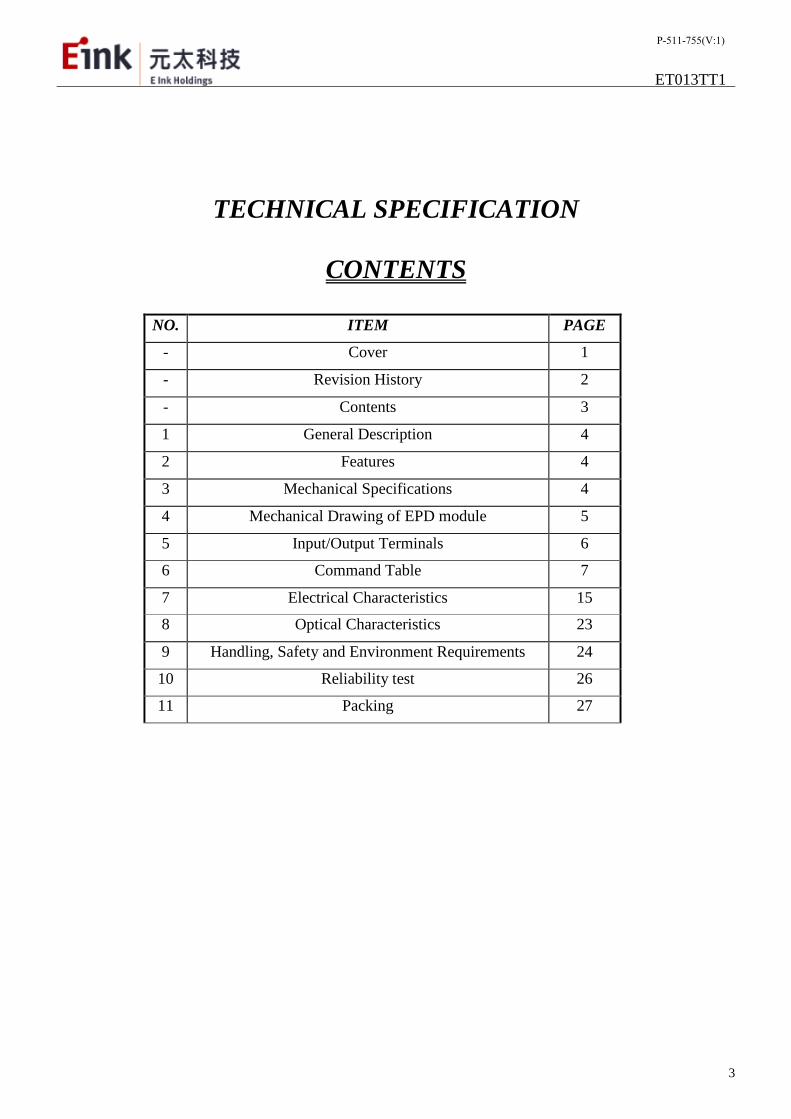
NO. ITEM PAGE
- Cover 1
- Revision History 2
- Contents 3
1 General Description 4
2 Features 4
3 Mechanical Specifications 4
4 Mechanical Drawing of EPD module 5
5 Input/Output Terminals 6
6 Command Table 7
7 Electrical Characteristics 15
8 Optical Characteristics 23
9 Handling, Safety and Environment Requirements 24
10 Reliability test 26
11 Packing 27
P-511-755(V:1)

ET013TT1
4
1. General Description
The 1.3 inch EPD is a reflective electrophoretic E Ink technology display module based on
active matrix TFT and plastic substrate. It has 1.3 inch active area with 256 x 256 pixels, the display is
capable to display images at black and white (1 bit only) depending on the display controller and the
associated waveform file it used.
2. Features
High contrast reflective /electrophoretic technology.
256 x 256 display
High reflectance
Ultra wide viewing angle
Pure reflective mode
Bi-stable
Commercial temperature range
Plastic substrate.
3. Mechanical Specifications
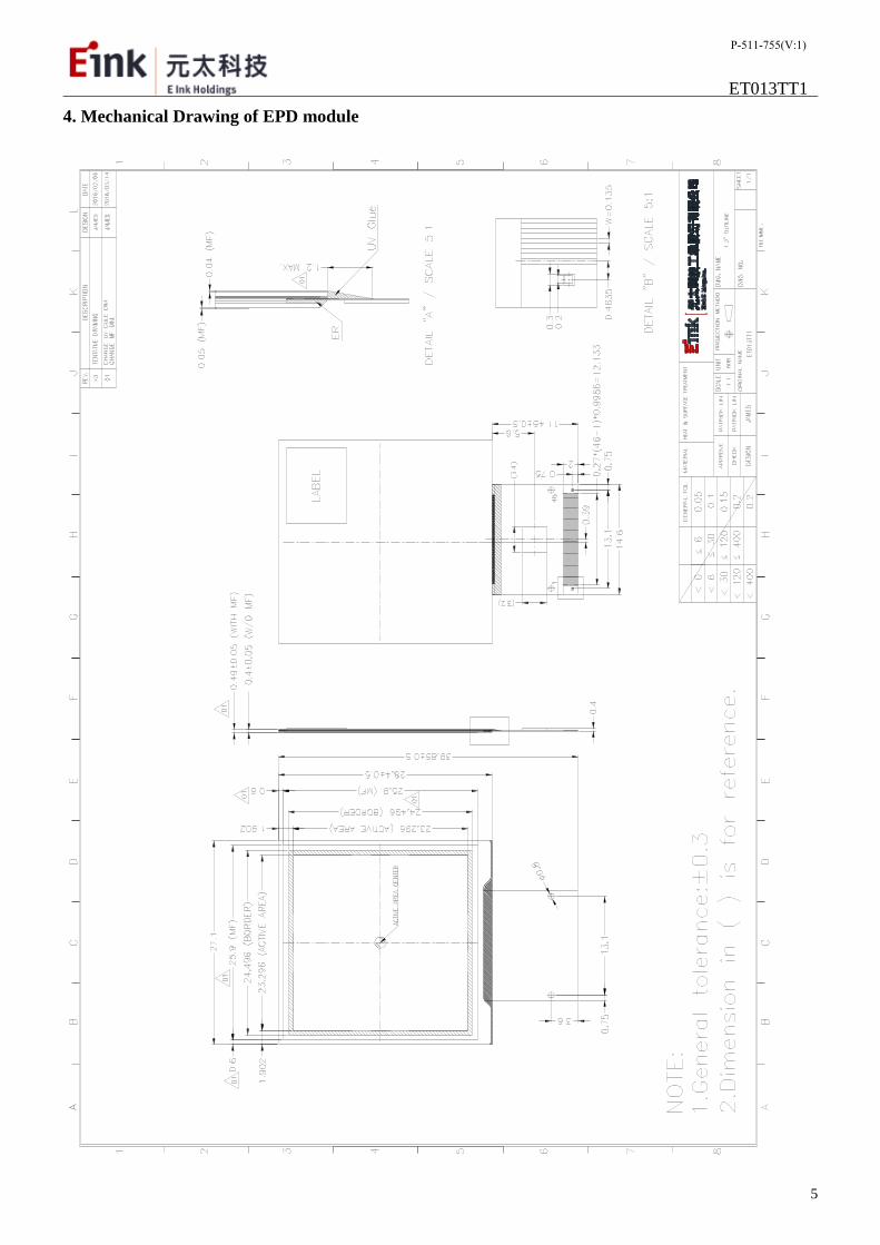
Parameter Specifications Unit RemarkScreen Size 1.3 Inch
Display Resolution 256 (H) × 256 (V) PixelActive Area 23.296 (H) × 23.296 (V) mmPixel Pitch 0.091 (H) × 0.091 (V) mm
Pixel Configuration SquareOutline Dimension 27.1(H) × 28.4 (V) × 0.4 (D) mm
Weight 0.4+0.04 gw/o masking
film
P-511-755(V:1)
ET013TT1
5
4. Mechanical Drawing of EPD module
P-511-755(V:1)

ET013TT1
6
5. Input / Output Terminals
I: Input O: Output P: Power C: Charge pump
Pin # Signal I/O Description Remark
1 VCOM_P I Common Connection
2 VCOM_IC O VCOM output
3 VCC P Analog power (2.3V ~ 3.6V)
4 VDD P Digital power (2.3V ~ 3.6V)
5 GND P Ground
6 VGH P Positive power supply for gate driver
7 VGL P Negative power supply for gate driver
8 VDH P Positive power supply for source driver
9 VDL P Negative power supply for source driver
10 CSB I SPI chip select (low active)
11 BUSY O Internal operation busy flag (1 : Driver is busy)
12 SCL I SPI serial clock
13 SDI I SPI serial data input
I2C Mode : Serial data input/output (10K pull-up R)14 SDO O SPI serial data output (floating in idle state)
15 RESETB I Global reset pin (low active)
16 TEST2 -- Test pin, keeps open
17 OEI I Gate output enable pin
18 VDHR P Positive source driver voltage (low voltage)
19 VCL P Negative power supply for VCOM low voltage level
20 C8N C Capacitor 9 connection pin for booster 3 circuit (VCL)
21 C8P C Capacitor 9 connection pin for booster 3 circuit (VCL)
22 C7N C Capacitor 8 connection pin for booster 2 circuit (VGL/VDL)
23 C7P C Capacitor 8 connection pin for booster 2 circuit (VGL/VDL)
24 C6N C Capacitor 7 connection pin for booster 2 circuit (VGL/VDL)
25 C6P C Capacitor 7 connection pin for booster 2 circuit (VGL/VDL)
26 C5N C Capacitor 6 connection pin for booster 1 circuit (VGH/VDH)
27 C5P C Capacitor 6 connection pin for booster 1 circuit (VGH/VDH)
28 C4N C Capacitor 5 connection pin for booster 1 circuit (VGH/VDH)
29 C4P C Capacitor 5 connection pin for booster 1 circuit (VGH/VDH)
30 C3N C Capacitor 4 connection pin for booster 1 circuit (VGH/VDH)
31 C3P C Capacitor 4 connection pin for booster 1 circuit (VGH/VDH)
P-511-755(V:1)

ET013TT1
7
32 C2N C Capacitor 3 connection pin for booster 1 circuit (VGH/VDH)
33 C2P C Capacitor 3 connection pin for booster 1 circuit (VGH/VDH)
34 C1N C Capacitor 2 connection pin for booster 1 circuit (VGH/VDH)
35 C1P C Capacitor 2 connection pin for booster 1 circuit (VGH/VDH)
36 GND P Ground
37 VPP C Capacitor 1 connection pin for booster 1 circuit (VGH/VDH)
38 VCOM_IC O VCOM output
39 VCC P Analog power (2.3V ~ 3.6V)
40 VDD P Digital power (2.3V ~ 3.6V)
41 GND P Ground
42 VGH P Positive power supply for gate driver
43 VGL P Negative power supply for gate driver
44 VDH P Positive power supply for source driver
45 VDL P Negative power supply for source driver
46 VCOM_P I Common Connection
P-511-755(V:1)

ET013TT1
8
6. Command Table
# Command Index A0 R/W D7 D6 D5 D4 D3 D2 D1 D0 Default1. Index -- 0 W 0 0 0 0 IDX3 IDX2 IDX1 IDX0 00H
2. Read Device ID -- 0 R BUSY 0 0 0 0 ID2 ID1 ID0 00H
3. Pump Status 00H 1 R LVDS VCPOK 0 0 0 0 0 0 00H
4. Channel Setting 01H 1 R/WC[7:0] FFH
C[15:8] FFH
C[23:16] FFH
5. Pump Setting (1) 04H 1 R/W DIS_VH 0 CPDISM[1:0] CPS[1:0] CPM[1:0] 0FH
6. Pump Setting (2) 05H 1 R/W 0 0 0 0 VCON EN_VCL EN_VN EN_VH 00H
7. OSC & Power setting 07H 1 R/W 0 OSCM[1:0] OSCON 0 CPEXT 0 0 40H
8. Thermal Sensor Setting 08H 1 R/W 0 0 0 0 0 LVDEN BGON TSON 00H
9. PWM Width Select 09H 1 R/W P[7:0] 00H
10. Write Gate/Source Data(49-byte command) 0AH
1 W O0[1:0] O1[1:0] O2[1:0] O3[1:0] 00H
1 W : : : : 00H
1 W O188[1:0] O189[1:0] O190[1:0] O191[1:0] 00H
11. Read Sensor Register 0FH 1 R 0 T[6:0] 00H
P-511-755(V:1)
ET013TT1
9
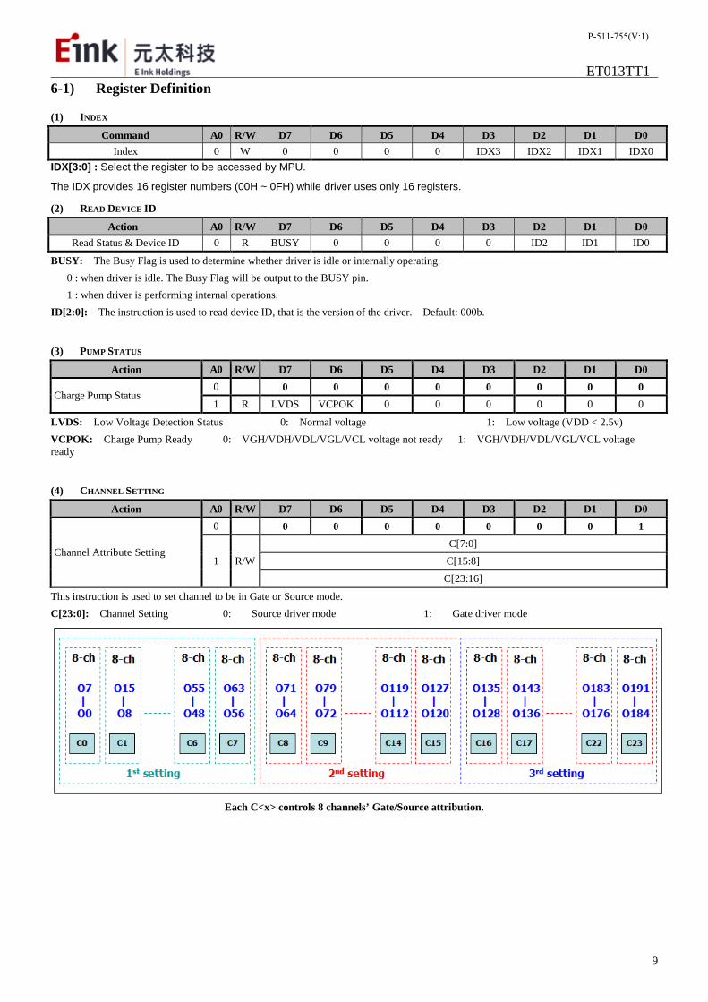
6-1) Register Definition
(1) INDEX
Command A0 R/W D7 D6 D5 D4 D3 D2 D1 D0
Index 0 W 0 0 0 0 IDX3 IDX2 IDX1 IDX0
IDX[3:0] : Select the register to be accessed by MPU.
The IDX provides 16 register numbers (00H ~ 0FH) while driver uses only 16 registers.
(2) READ DEVICE ID
Action A0 R/W D7 D6 D5 D4 D3 D2 D1 D0
Read Status & Device ID 0 R BUSY 0 0 0 0 ID2 ID1 ID0
BUSY: The Busy Flag is used to determine whether driver is idle or internally operating.
0 : when driver is idle. The Busy Flag will be output to the BUSY pin.
1 : when driver is performing internal operations.
ID[2:0]: The instruction is used to read device ID, that is the version of the driver. Default: 000b.
(3) PUMP STATUS
Action A0 R/W D7 D6 D5 D4 D3 D2 D1 D0
Charge Pump Status0 0 0 0 0 0 0 0 0
1 R LVDS VCPOK 0 0 0 0 0 0
LVDS: Low Voltage Detection Status 0: Normal voltage 1: Low voltage (VDD < 2.5v)
VCPOK: Charge Pump Ready 0: VGH/VDH/VDL/VGL/VCL voltage not ready 1: VGH/VDH/VDL/VGL/VCL voltageready
(4) CHANNEL SETTING
Action A0 R/W D7 D6 D5 D4 D3 D2 D1 D0
Channel Attribute Setting
0 0 0 0 0 0 0 0 1
1 R/W
C[7:0]
C[15:8]
C[23:16]
This instruction is used to set channel to be in Gate or Source mode.
C[23:0]: Channel Setting 0: Source driver mode 1: Gate driver mode
Each C<x> controls 8 channels’ Gate/Source attribution.
P-511-755(V:1)
ET013TT1
10
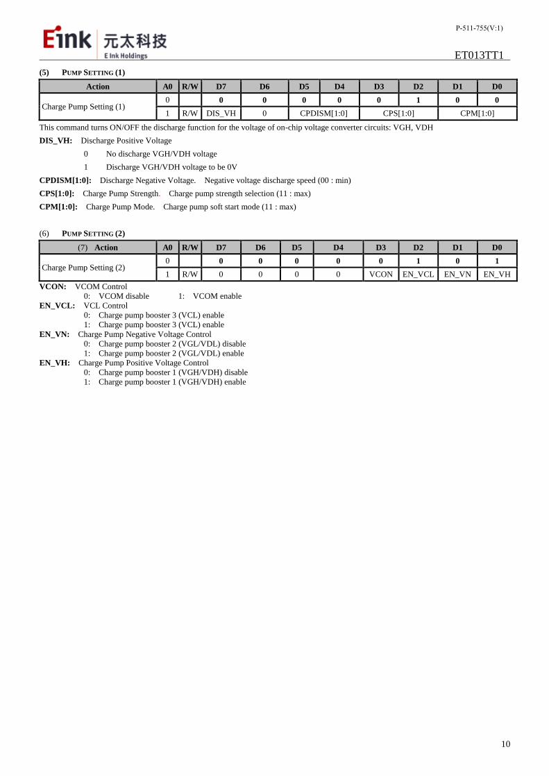
(5) PUMP SETTING (1)
Action A0 R/W D7 D6 D5 D4 D3 D2 D1 D0
Charge Pump Setting (1)0 0 0 0 0 0 1 0 0
1 R/W DIS_VH 0 CPDISM[1:0] CPS[1:0] CPM[1:0]
This command turns ON/OFF the discharge function for the voltage of on-chip voltage converter circuits: VGH, VDH
DIS_VH: Discharge Positive Voltage
0 No discharge VGH/VDH voltage
1 Discharge VGH/VDH voltage to be 0V
CPDISM[1:0]: Discharge Negative Voltage. Negative voltage discharge speed (00 : min)
CPS[1:0]: Charge Pump Strength. Charge pump strength selection (11 : max)
CPM[1:0]: Charge Pump Mode. Charge pump soft start mode (11 : max)
(6) PUMP SETTING (2)
(7) Action A0 R/W D7 D6 D5 D4 D3 D2 D1 D0
Charge Pump Setting (2)0 0 0 0 0 0 1 0 1
1 R/W 0 0 0 0 VCON EN_VCL EN_VN EN_VH
VCON: VCOM Control0: VCOM disable 1: VCOM enable
EN_VCL: VCL Control0: Charge pump booster 3 (VCL) enable1: Charge pump booster 3 (VCL) enable
EN_VN: Charge Pump Negative Voltage Control0: Charge pump booster 2 (VGL/VDL) disable1: Charge pump booster 2 (VGL/VDL) enable
EN_VH: Charge Pump Positive Voltage Control0: Charge pump booster 1 (VGH/VDH) disable1: Charge pump booster 1 (VGH/VDH) enable
P-511-755(V:1)

ET013TT1
11
(7) OSC & POWER SETTING
Action A0 R/W D7 D6 D5 D4 D3 D2 D1 D0
System Clock Rate Setting0 0 0 0 0 0 1 1 1
1 R/W 0 OSCM[1:0] OSCON 0 CPEXT 0 0
OSCM[1:0]: System Clock Rate Selection
00b: 250K Hz 01b: 500K Hz 10b: 1M Hz 11b: 2M Hz
OSCON: OSC Clock Enable 0: System clock disable 1: System clock enable
CPEXT: External Power Voltage
0: Internal charge pump as power (VGH/VDH/VDL/VGL/VCL) source
1: External power voltage as power source
(8) THERMAL SENSOR SETTING
Action A0 R/W D7 D6 D5 D4 D3 D2 D1 D0
Thermal Sensor Setting0 0 0 0 0 1 0 0 0
1 R/W 0 0 0 0 0 LVDEN BGON TSON
LVDEN : This register is used to enable LVDS.
0 : LVDS Disable 1 : LVDS Enable
BGON : This register determines the band-gap circuit to be ON or OFF.
0 / 1 : the band-gap circuit is turn OFF / ON.
TSON : This register determines the temperature sensor to be ON or OFF.
0 / 1 : the temperature sensor is turn OFF / ON.
P-511-755(V:1)
ET013TT1
12
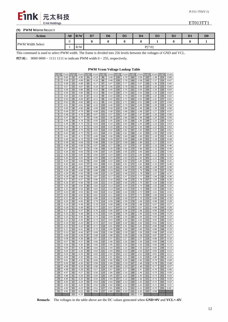
(9) PWM WIDTH SELECT
Action A0 R/W D7 D6 D5 D4 D3 D2 D1 D0
PWM Width Select0 0 0 0 0 1 0 0 1
1 R/W P[7:0]
This command is used to select PWM width. The frame is divided into 256 levels between the voltages of GND and VCL.
P[7:0] : 0000 0000 ~ 1111 1111 to indicate PWM width 0 ~ 255, respectively.
PWM Vcom Voltage Lookup TableP[7:0] Vcom P[7:0] Vcom P[7:0] Vcom P[7:0] Vcom P[7:0] Vcom P[7:0] Vcom P[7:0] Vcom P[7:0] Vcom
0 -5.60 32 -4.90 64 -4.19 96 -3.49 128 -2.79 160 -2.09 192 -1.38 224 -0.680 -5.59 32 -4.89 64 -4.18 96 -3.48 128 -2.78 160 -2.08 192 -1.37 224 -0.671 -5.58 33 -4.88 65 -4.17 97 -3.47 129 -2.77 160 -2.07 193 -1.36 225 -0.661 -5.57 33 -4.87 65 -4.16 97 -3.46 129 -2.76 161 -2.06 193 -1.35 225 -0.652 -5.56 33 -4.86 66 -4.15 98 -3.45 130 -2.75 161 -2.05 194 -1.34 226 -0.642 -5.55 34 -4.85 66 -4.14 98 -3.44 130 -2.74 162 -2.04 194 -1.33 226 -0.632 -5.54 34 -4.84 67 -4.13 99 -3.43 130 -2.73 162 -2.03 195 -1.32 226 -0.623 -5.53 35 -4.83 67 -4.12 99 -3.42 131 -2.72 163 -2.02 195 -1.31 227 -0.613 -5.52 35 -4.82 68 -4.11 99 -3.41 131 -2.71 163 -2.01 196 -1.30 227 -0.604 -5.51 36 -4.81 68 -4.10 100 -3.40 132 -2.70 164 -2.00 196 -1.29 228 -0.594 -5.50 36 -4.80 68 -4.09 100 -3.39 132 -2.69 164 -1.99 196 -1.28 228 -0.585 -5.49 37 -4.79 69 -4.08 101 -3.38 133 -2.68 165 -1.98 197 -1.27 229 -0.575 -5.48 37 -4.78 69 -4.07 101 -3.37 133 -2.67 165 -1.97 197 -1.26 229 -0.566 -5.47 38 -4.77 70 -4.06 102 -3.36 134 -2.66 165 -1.96 198 -1.25 230 -0.556 -5.46 38 -4.76 70 -4.05 102 -3.35 134 -2.65 166 -1.95 198 -1.24 230 -0.547 -5.45 38 -4.75 71 -4.04 103 -3.34 135 -2.64 166 -1.94 199 -1.23 231 -0.537 -5.44 39 -4.74 71 -4.03 103 -3.33 135 -2.63 167 -1.93 199 -1.22 231 -0.527 -5.43 39 -4.73 72 -4.02 104 -3.32 135 -2.62 167 -1.92 200 -1.21 232 -0.518 -5.42 40 -4.72 72 -4.01 104 -3.31 136 -2.61 168 -1.91 200 -1.20 232 -0.508 -5.41 40 -4.71 73 -4.00 104 -3.30 136 -2.60 168 -1.90 201 -1.19 232 -0.499 -5.40 41 -4.70 73 -3.99 105 -3.29 137 -2.59 169 -1.89 201 -1.18 233 -0.489 -5.39 41 -4.69 73 -3.98 105 -3.28 137 -2.58 169 -1.88 201 -1.17 233 -0.47
10 -5.38 42 -4.68 74 -3.97 106 -3.27 138 -2.57 170 -1.87 202 -1.16 234 -0.4610 -5.37 42 -4.67 74 -3.96 106 -3.26 138 -2.56 170 -1.86 202 -1.15 234 -0.4511 -5.36 43 -4.66 75 -3.95 107 -3.25 139 -2.55 170 -1.85 203 -1.14 235 -0.4411 -5.35 43 -4.65 75 -3.94 107 -3.24 139 -2.54 171 -1.84 203 -1.13 235 -0.4312 -5.34 43 -4.64 76 -3.93 108 -3.23 140 -2.53 171 -1.83 204 -1.12 236 -0.4212 -5.33 44 -4.63 76 -3.92 108 -3.22 140 -2.52 172 -1.82 204 -1.11 236 -0.4112 -5.32 44 -4.62 77 -3.91 109 -3.21 140 -2.51 172 -1.81 205 -1.10 237 -0.4013 -5.31 45 -4.61 77 -3.90 109 -3.20 141 -2.50 173 -1.80 205 -1.09 237 -0.3913 -5.30 45 -4.60 78 -3.89 109 -3.19 141 -2.49 173 -1.79 206 -1.08 237 -0.3814 -5.29 46 -4.59 78 -3.88 110 -3.18 142 -2.48 174 -1.78 206 -1.07 238 -0.3714 -5.28 46 -4.58 79 -3.87 110 -3.17 142 -2.47 174 -1.77 206 -1.06 238 -0.3615 -5.27 47 -4.57 79 -3.86 111 -3.16 143 -2.46 175 -1.76 207 -1.05 239 -0.3515 -5.26 47 -4.56 79 -3.85 111 -3.15 143 -2.45 175 -1.75 207 -1.04 239 -0.3416 -5.25 48 -4.55 80 -3.84 112 -3.14 144 -2.44 175 -1.74 208 -1.03 240 -0.3316 -5.24 48 -4.54 80 -3.83 112 -3.13 144 -2.43 176 -1.73 208 -1.02 240 -0.3217 -5.23 48 -4.53 81 -3.82 113 -3.12 145 -2.42 176 -1.72 209 -1.01 241 -0.3117 -5.22 49 -4.52 81 -3.81 113 -3.11 145 -2.41 177 -1.71 209 -1.00 241 -0.3017 -5.21 49 -4.51 82 -3.80 114 -3.10 145 -2.40 177 -1.70 210 -0.99 242 -0.2918 -5.20 50 -4.50 82 -3.79 114 -3.09 146 -2.39 178 -1.69 210 -0.98 242 -0.2818 -5.19 50 -4.49 83 -3.78 114 -3.08 146 -2.38 178 -1.68 211 -0.97 242 -0.2719 -5.18 51 -4.48 83 -3.77 115 -3.07 147 -2.37 179 -1.67 211 -0.96 243 -0.2619 -5.17 51 -4.47 84 -3.76 115 -3.06 147 -2.36 179 -1.66 211 -0.95 243 -0.2520 -5.16 52 -4.46 84 -3.75 116 -3.05 148 -2.35 180 -1.65 212 -0.94 244 -0.2420 -5.15 52 -4.45 84 -3.74 116 -3.04 148 -2.34 180 -1.64 212 -0.93 244 -0.2321 -5.14 53 -4.44 85 -3.73 117 -3.03 149 -2.33 181 -1.63 213 -0.92 245 -0.2221 -5.13 53 -4.43 85 -3.72 117 -3.02 149 -2.32 181 -1.62 213 -0.91 245 -0.2122 -5.12 53 -4.42 86 -3.71 118 -3.01 150 -2.31 181 -1.61 214 -0.90 246 -0.2022 -5.11 54 -4.41 86 -3.70 118 -3.00 150 -2.30 182 -1.60 214 -0.89 246 -0.1922 -5.10 54 -4.40 87 -3.69 119 -2.99 150 -2.29 182 -1.59 215 -0.88 247 -0.1823 -5.09 55 -4.39 87 -3.68 119 -2.98 151 -2.28 183 -1.58 215 -0.87 247 -0.1723 -5.08 55 -4.38 88 -3.67 119 -2.97 151 -2.27 183 -1.57 216 -0.86 247 -0.1624 -5.07 56 -4.37 88 -3.66 120 -2.96 152 -2.26 184 -1.56 216 -0.85 248 -0.1524 -5.06 56 -4.36 89 -3.65 120 -2.95 152 -2.25 184 -1.55 216 -0.84 248 -0.1425 -5.05 57 -4.35 89 -3.64 121 -2.94 153 -2.24 185 -1.54 217 -0.83 249 -0.1325 -5.04 57 -4.34 89 -3.63 121 -2.93 153 -2.23 185 -1.53 217 -0.82 249 -0.1226 -5.03 58 -4.33 90 -3.62 122 -2.92 154 -2.22 186 -1.52 218 -0.81 250 -0.1126 -5.02 58 -4.32 90 -3.61 122 -2.91 154 -2.21 186 -1.51 218 -0.80 250 -0.1027 -5.01 58 -4.31 91 -3.60 123 -2.90 155 -2.20 186 -1.50 219 -0.79 251 -0.0927 -5.00 59 -4.30 91 -3.59 123 -2.89 155 -2.19 187 -1.49 219 -0.78 251 -0.0828 -4.99 59 -4.29 92 -3.58 124 -2.88 155 -2.18 187 -1.48 220 -0.77 252 -0.0728 -4.98 60 -4.28 92 -3.57 124 -2.87 156 -2.17 188 -1.47 220 -0.76 252 -0.0628 -4.97 60 -4.27 93 -3.56 124 -2.86 156 -2.16 188 -1.46 221 -0.75 252 -0.0529 -4.96 61 -4.26 93 -3.55 125 -2.85 157 -2.15 189 -1.45 221 -0.74 253 -0.0429 -4.95 61 -4.25 94 -3.54 125 -2.84 157 -2.14 189 -1.44 221 -0.73 253 -0.0330 -4.94 62 -4.24 94 -3.53 126 -2.83 158 -2.13 190 -1.43 222 -0.72 254 -0.0230 -4.93 62 -4.23 94 -3.52 126 -2.82 158 -2.12 190 -1.42 222 -0.71 254 -0.0131 -4.92 63 -4.22 95 -3.51 127 -2.81 159 -2.11 191 -1.41 223 -0.70 255 0.0031 -4.91 63 -4.21 95 -3.50 127 -2.80 159 -2.10 191 -1.40 223 -0.69
63 -4.20 191 -1.39
Remark: The voltages in the table above are the DC values generated when GND=0V and VCL=–6V.
P-511-755(V:1)

ET013TT1
13
P-511-755(V:1)
ET013TT1
14
(10) WRITE GATE/SOURCE DATA (49-BYTE COMMAND)
Action A0 R/W D7 D6 D5 D4 D3 D2 D1 D0
Write Gate/Source Data(49-byte command)
0 0 0 0 0 1 0 1 0
1 W O0[1:0] O1[1:0] O2[1:0] O3[1:0]
1 W : : : :
1 W O188[1:0] O189[1:0] O190[1:0] O191[1:0]
The command is used to write the display data to the 384-bit register stage. Each two bits of the register stage decides the input of the DriverChannel. When EPD is displaying, it is needed to write data continuously.
Gate/Source Channels
1st written byte 2nd written byte … 48th written byte
4-channel 4-channel … 4-channel
O0 O1 O2 O3 O4 O5 O6 O7 … O188 O189 O190 O191
D[7:6] D[5:4] D[3:2] D[1:0] D[7:6] D[5:4] D[3:2] D[1:0] … D[7:6] D[5:4] D[3:2] D[1:0]
Gate/Source Data Definition
D[7:6], D[5:4], D[3:2], D[1:0]
00 01 10 11
Source Mode (C=0) 0 0 VDL VDH
Gate Mode (C=1) VGL VGH VGL VGH
(11) READ SENSOR REGISTER
Action A0 R/W D7 D6 D5 D4 D3 D2 D1 D0
Read Sensor Register0 0 0 0 0 1 1 1 1
1 R 0 T[6:0]
T[6:0] : Temperature Range selection. -20~+70 oC
T[4:0] Temp. Range ( oC) T[4:0] Temp. Range ( oC) T[4:0] Temp. Range ( oC)
000 0000 0 ~ 2 001 0000 32 ~ 34 010 0000 64 ~ 66
000 0001 2 ~ 4 001 0001 34 ~ 36 010 0001 66 ~ 68
000 0010 4 ~ 6 001 0010 36 ~ 38 010 0010 68 ~ 70
000 0011 6 ~ 8 001 0011 38 ~ 40 --
000 0100 8 ~ 10 001 0100 40 ~ 42 --
000 0101 10 ~ 12 001 0101 42 ~ 44 --
000 0110 12 ~ 14 001 0110 44 ~ 46 111 0110 -20 ~ -18
000 0111 14 ~ 16 001 0111 46 ~ 48 111 0111 -18 ~ -16
000 1000 16 ~ 18 001 1000 48 ~ 50 111 1000 -16 ~ -14
000 1001 18 ~ 20 001 1001 50 ~ 52 111 1001 -14 ~ -12
000 1010 20 ~ 22 001 1010 52 ~ 54 111 1010 -12 ~ -10
000 1011 22 ~ 24 001 1011 54 ~ 56 111 1011 -10 ~ -8
000 1100 24 ~ 26 001 1100 56 ~ 58 111 1100 -8 ~ -6
000 1101 26 ~ 28 001 1101 58 ~ 60 111 1101 -6 ~ -4
000 1110 28 ~ 30 001 1110 60 ~ 62 111 1110 -4 ~ -2
000 1111 30 ~ 32 001 1111 62 ~ 64 111 1111 -2 ~ 0
P-511-755(V:1)

ET013TT1
15
7. Electrical Characteristics
7-1) Absolute maximum rating
Signal Parameter Condition Rating Unit
VDD Supply voltage range -0.3 to 6 V
VIN Input voltage range -0.3 to VDD + 0.3 V
TOPR Operating temperature range 0 to 50 oC
TSTR Storage temperature range -25 to 70 oC
Note: Absolute Maximum Ratings are stress ratings. Stresses higher than those listed above may cause permanent damage tothe device. Functional operation of the device at these or any other conditions above those indicated in the operation sectionsof this specification is not implied. Exposure to absolute maximum rating conditions for extended periods may affect devicereliability.
7-2) DC characteristics
(VDD = 2.3 to 3.6V, Ta = 25oC)
Item Symbol Condition Min. Typ. Max. Unit
Operating VoltageVDD 2.3 3.3 3.6 V
VCC 2.3 3.3 3.6 V
Input voltageHigh VIH 0.8xVDD
VLow VIL 0.2xVDD
Output voltageHigh VOH IOH = 0.5mA 0.8xVDD
VLow VOL IOL = -0.5mA 0.2xVDD
I/O pad Input leakage current IIL VIN = VDD or Vss 1 uA
EPD driver ONResistance
RON Ta = 25oC 50K R
Oscillator frequency Fosc fOSC Ta = 25oC -10% 2M +10% Hz
Voltage converterOutput voltage
VDH2.3≦VCC <2.5V
2.5≦VCC ≦3.6V13~14
1414 V
Voltage converterOutput voltage
VGH VCC=2.3~3.6V 19 19 V
Voltage converterOutput voltage
VDL2.3≦VCC <2.5V
2.5≦VCC ≦3.6V-14
-13~-14-14
V
Voltage converterOutput voltage
VGL VCC=2.3~3.6V -19 -19 V
Voltage converterOutput voltage
Vcom -2xVCC 0 V
Panel Power P 27.8 57.3 mW
- The Maximum power consumption is measured with following pattern transition: from pattern of repeated 1 consecutive black scan
lines followed by 1 consecutive white scan line to that of repeated white scan lines followed by 1 consecutive black scan lines. (Note
7-1)
- The Typical power consumption is measured with following pattern transition: from horizontal black and white pattern to vertical
black and white pattern. (Note 7-2)
- The listed electrical/optical characteristics are only guaranteed under the controller & waveform provided by E Ink
- Vcom is recommended to be set in the range of assigned value ± 0.1V.
P-511-755(V:1)

ET013TT1
16
Note7-1:
The maximum power consumption
Note7-2:
The Typical power consumption
P-511-755(V:1)

ET013TT1
17
7-3) AC characteristics
Serial Bus Timing Characteristics (for Serial MCU)
Symbol Parameter Conditions Min Typ Max UnittCYS Serial 50 nS
tWHS SCLK 25 nS
tWLS SCLK 25 nS
tDSS Data 12 nS
tDHS Data 12 nS
tCSS CSB 12 nS
tCHS CSB 20 nS
P-511-755(V:1)

ET013TT1
18
(1)For typical Read/Write data command
Example:
Command: Read Device ID
P-511-755(V:1)

ET013TT1
19
Command: Thermal Sensor Setting
(2) For Channel setting and Write data command
P-511-755(V:1)
ET013TT1
20
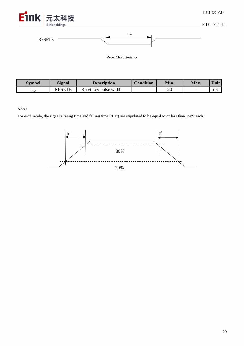
RST
tRW
Reset Characteristics
Symbol Signal Description Condition Min. Max. UnittRW RESETB Reset low pulse width 20 – uS
Note:
For each mode, the signal’s rising time and falling time (tf, tr) are stipulated to be equal to or less than 15nS each.
20%
80%
tf
15nS
tr
15nS
RESETB
P-511-755(V:1)

ET013TT1
21
7-5) Power ON / Power OFF Sequence
Power ON Sequence
Power OFF Sequence
P-511-755(V:1)

ET013TT1
22
7-6) Reference Circuit
P-511-755(V:1)
ET013TT1
23
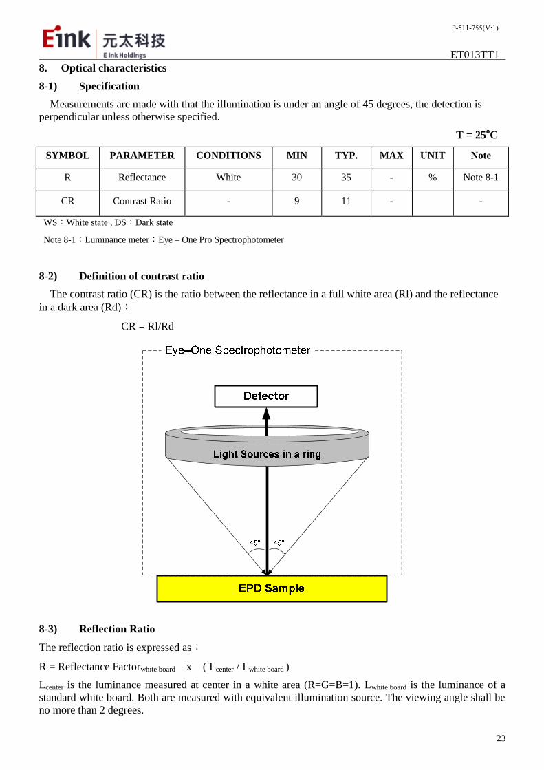
8. Optical characteristics
8-1) Specification
Measurements are made with that the illumination is under an angle of 45 degrees, the detection isperpendicular unless otherwise specified.
T = 25oC
SYMBOL PARAMETER CONDITIONS MIN TYP. MAX UNIT Note
R Reflectance White 30 35 - % Note 8-1
CR Contrast Ratio - 9 11 - -
WS:White state , DS:Dark state
Note 8-1:Luminance meter:Eye – One Pro Spectrophotometer
8-2) Definition of contrast ratio
The contrast ratio (CR) is the ratio between the reflectance in a full white area (Rl) and the reflectancein a dark area (Rd):
CR = Rl/Rd
8-3) Reflection Ratio
The reflection ratio is expressed as:
R = Reflectance Factorwhite board x ( Lcenter / Lwhite board )
Lcenter is the luminance measured at center in a white area (R=G=B=1). Lwhite board is the luminance of astandard white board. Both are measured with equivalent illumination source. The viewing angle shall beno more than 2 degrees.
P-511-755(V:1)
ET013TT1
24
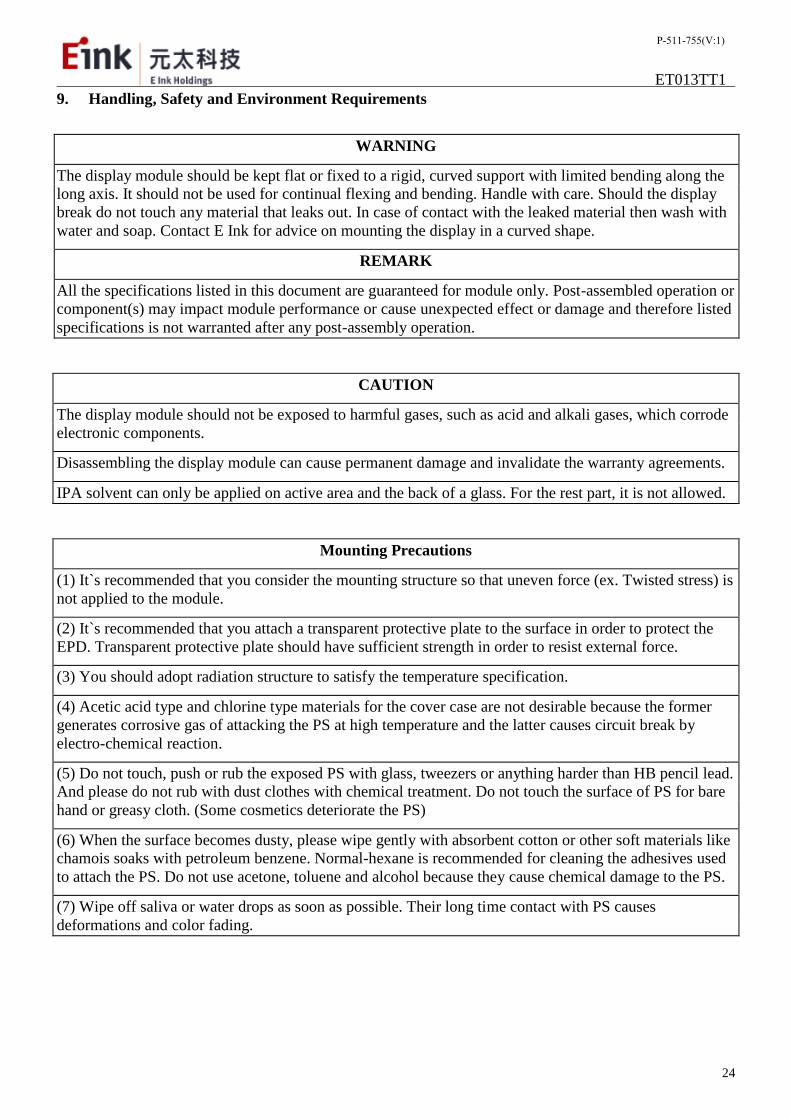
9. Handling, Safety and Environment Requirements
WARNING
The display module should be kept flat or fixed to a rigid, curved support with limited bending along thelong axis. It should not be used for continual flexing and bending. Handle with care. Should the displaybreak do not touch any material that leaks out. In case of contact with the leaked material then wash withwater and soap. Contact E Ink for advice on mounting the display in a curved shape.
REMARK
All the specifications listed in this document are guaranteed for module only. Post-assembled operation orcomponent(s) may impact module performance or cause unexpected effect or damage and therefore listedspecifications is not warranted after any post-assembly operation.
CAUTION
The display module should not be exposed to harmful gases, such as acid and alkali gases, which corrodeelectronic components.
Disassembling the display module can cause permanent damage and invalidate the warranty agreements.
IPA solvent can only be applied on active area and the back of a glass. For the rest part, it is not allowed.
Mounting Precautions
(1) It`s recommended that you consider the mounting structure so that uneven force (ex. Twisted stress) isnot applied to the module.
(2) It`s recommended that you attach a transparent protective plate to the surface in order to protect theEPD. Transparent protective plate should have sufficient strength in order to resist external force.
(3) You should adopt radiation structure to satisfy the temperature specification.
(4) Acetic acid type and chlorine type materials for the cover case are not desirable because the formergenerates corrosive gas of attacking the PS at high temperature and the latter causes circuit break byelectro-chemical reaction.
(5) Do not touch, push or rub the exposed PS with glass, tweezers or anything harder than HB pencil lead.And please do not rub with dust clothes with chemical treatment. Do not touch the surface of PS for barehand or greasy cloth. (Some cosmetics deteriorate the PS)
(6) When the surface becomes dusty, please wipe gently with absorbent cotton or other soft materials likechamois soaks with petroleum benzene. Normal-hexane is recommended for cleaning the adhesives usedto attach the PS. Do not use acetone, toluene and alcohol because they cause chemical damage to the PS.
(7) Wipe off saliva or water drops as soon as possible. Their long time contact with PS causesdeformations and color fading.
P-511-755(V:1)
ET013TT1
25
Data sheet status
Product specification This data sheet contains final product specifications.
Limiting values
Limiting values given are in accordance with the Absolute Maximum Rating System (IEC 134). Stressabove one or more of the limiting values may cause permanent damage to the device. These are stressratings only and operation of the device at these or at any other conditions above those given in theCharacteristics sections of the specification is not implied. Exposure to limiting values for extendedperiods may affect device reliability.
Application information
Where application information is given, it is advisory and does not form part of the specification.
P-511-755(V:1)
ET013TT1
26
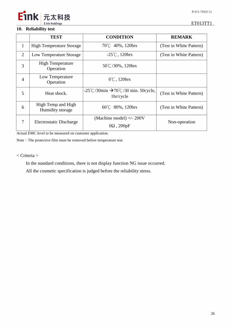
10. Reliability test
TEST CONDITION REMARK
1 High Temperature Storage 70℃ 40%, 120hrs (Test in White Pattern)
2 Low Temperature Storage -25℃, 120hrs (Test in White Pattern)
3High Temperature
Operation50℃/30%, 120hrs
4Low Temperature
Operation0℃, 120hrs
5 Heat shock.-25℃/30min70℃/30 min. 50cycle,
1hr/cycle(Test in White Pattern)
6High Temp and High
Humidity storage60℃ 80%, 120hrs (Test in White Pattern)
7 Electrostatic Discharge(Machine model) +/- 200V
0Ω , 200pFNon-operation
Actual EMC level to be measured on customer application.
Note:The protective film must be removed before temperature test.
< Criteria >
In the standard conditions, there is not display function NG issue occurred.
All the cosmetic specification is judged before the reliability stress.
P-511-755(V:1)
ET013TT1
27
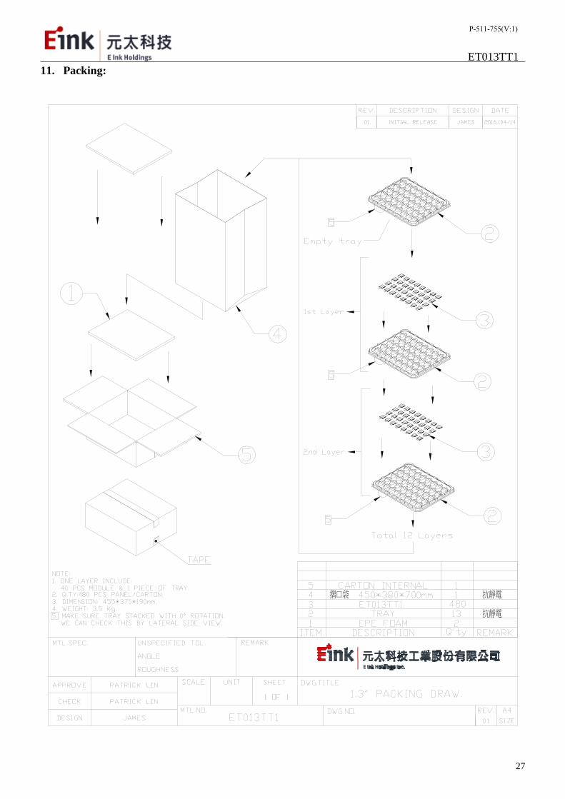
11. Packing:
P-511-755(V:1)


