TECHNICAL bulletin - Acson International 2013... · · 2013-05-03technical bulletin applicable...
7
TECHNICAL BULLETIN APPLICABLE MODEL M(5)WM-J TECHNICAL BULLETIN NO. TB008M13 DATE 17.04.2013 SUPERCEDED BULLETIN NO. - EFFECTIVE DATE - © McQuay International 1 [SUBJECT] WALL MOUNTED: MAIN CONTROL MODULE (PRINTED CIRCUIT BOARD, PCB) - NEW [DETAILS OF CHANGE] Introducing new wall mounted unit main control module design (printed circuit board, PCB), Switch Mode Power Supply (SMPS) type (J II) to replace existing Transformer type (J I). With J II PCB, it is now able to connect wired handset (such as SLM3, SLM 8 & Netware 3) on the indoor unit. The differences between J I and J II PCB are as follow: J I PCB (EXISTING) J II PCB (NEW) Outlook Type Transformer SMPS Others 1. Not compatible with wired handset 2. Not compatible with networking solution (NIM) 1. Compatible with wired handset 2. Compatible with networking solution (NIM03 only) 3. Lighter in weight 4. Lower power consumption during standby mode
Transcript of TECHNICAL bulletin - Acson International 2013... · · 2013-05-03technical bulletin applicable...

TECHNICAL BULLETIN APPLICABLE MODEL
M(5)WM-J TECHNICAL BULLETIN NO. TB008M13
DATE 17.04.2013
SUPERCEDED BULLETIN NO. -
EFFECTIVE DATE -
© McQuay International 1
[SUBJECT] WALL MOUNTED: MAIN CONTROL MODULE (PRINTED CIRCUIT BOARD, PCB) - NEW
[DETAILS OF CHANGE]
Introducing new wall mounted unit main control module design (printed circuit board, PCB), Switch Mode Power Supply (SMPS) type (J II) to replace existing Transformer type (J I). With J II PCB, it is now able to connect wired handset (such as SLM3, SLM 8 & Netware 3) on the indoor unit. The differences between J I and J II PCB are as follow:
J I PCB (EXISTING) J II PCB (NEW)
Ou
tloo
k
Type
Transformer SMPS
Oth
ers
1. Not compatible with wired handset 2. Not compatible with networking solution
(NIM)
1. Compatible with wired handset 2. Compatible with networking solution
(NIM03 only) 3. Lighter in weight 4. Lower power consumption during standby
mode
TECHNICAL BULLETIN APPLICABLE MODEL
M(5)WM-J TECHNICAL BULLETIN NO. TB008M13
DATE 17.04.2013
SUPERCEDED BULLETIN NO. -
EFFECTIVE DATE -
© McQuay International 2
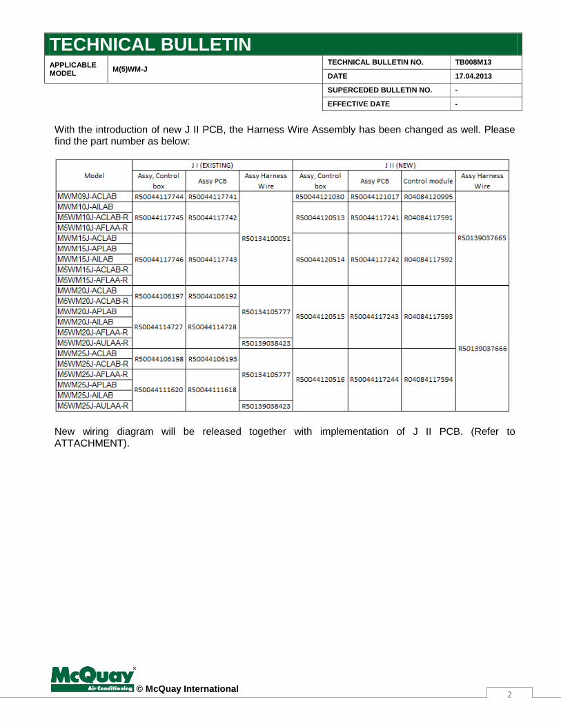
With the introduction of new J II PCB, the Harness Wire Assembly has been changed as well. Please find the part number as below:
New wiring diagram will be released together with implementation of J II PCB. (Refer to ATTACHMENT).

TECHNICAL BULLETIN APPLICABLE MODEL
M(5)WM-J TECHNICAL BULLETIN NO. TB008M13
DATE 17.04.2013
SUPERCEDED BULLETIN NO. -
EFFECTIVE DATE -
© McQuay International 3
[IMPLEMENTATION]
No MODEL STARTING BATCH
1 MWM09J-ACLAB
205615XX
2 MWM15J-ACLAB
3 MWM20J-ACLAB
4 MWM25J-ACLAB
5 M5WM10J-ACLAB-R
6 M5WM15J-ACLAB-R
7 M5WM20J-ACLAB-R
8 M5WM25J-ACLAB-R
9 M5WM20J-AULAA-R
10 M5WM25J-AULAA-R
11 M5WM10J-AFLAA-R
12 M5WM15J-AFLAA-R
13 M5WM20J-AFLAA-R
14 M5WM25J-AFLAA-R
15 MWM15J-APLAB
16 MWM20J-APLAB
17 MWM25J-APLAB
18 MWM10J-AILAB
19 MWM15J-AILAB 20 MWM20J-AILAB 21 MWM25J-AILAB

TECHNICAL BULLETIN APPLICABLE MODEL
M(5)WM-J TECHNICAL BULLETIN NO. TB008M13
DATE 17.04.2013
SUPERCEDED BULLETIN NO. -
EFFECTIVE DATE -
© McQuay International 4
[REMARK] The new J II PCB cannot be used to directly replace existing J I PCB. When J I PCB is to be replaced by J II PCB, the Assembly Harness Wire needs to be changed as well. Working instruction of replacing J I PCB with J II PCB are as follow:
Procedure:
1. Dismantle the indoor wires. 2. Unfasten the terminal block screw. 3. Change to new Assy. Harness Wire and fasten the terminal block screw. 4. Change to J II PCB and plug in the wires to J II PCB.
ganpwk
Text Box
Assy. Harness Wire
TECHNICAL BULLETIN APPLICABLE MODEL
M(5)WM-J TECHNICAL BULLETIN NO. TB008M13
DATE 17.04.2013
SUPERCEDED BULLETIN NO. -
EFFECTIVE DATE -
© McQuay International 5
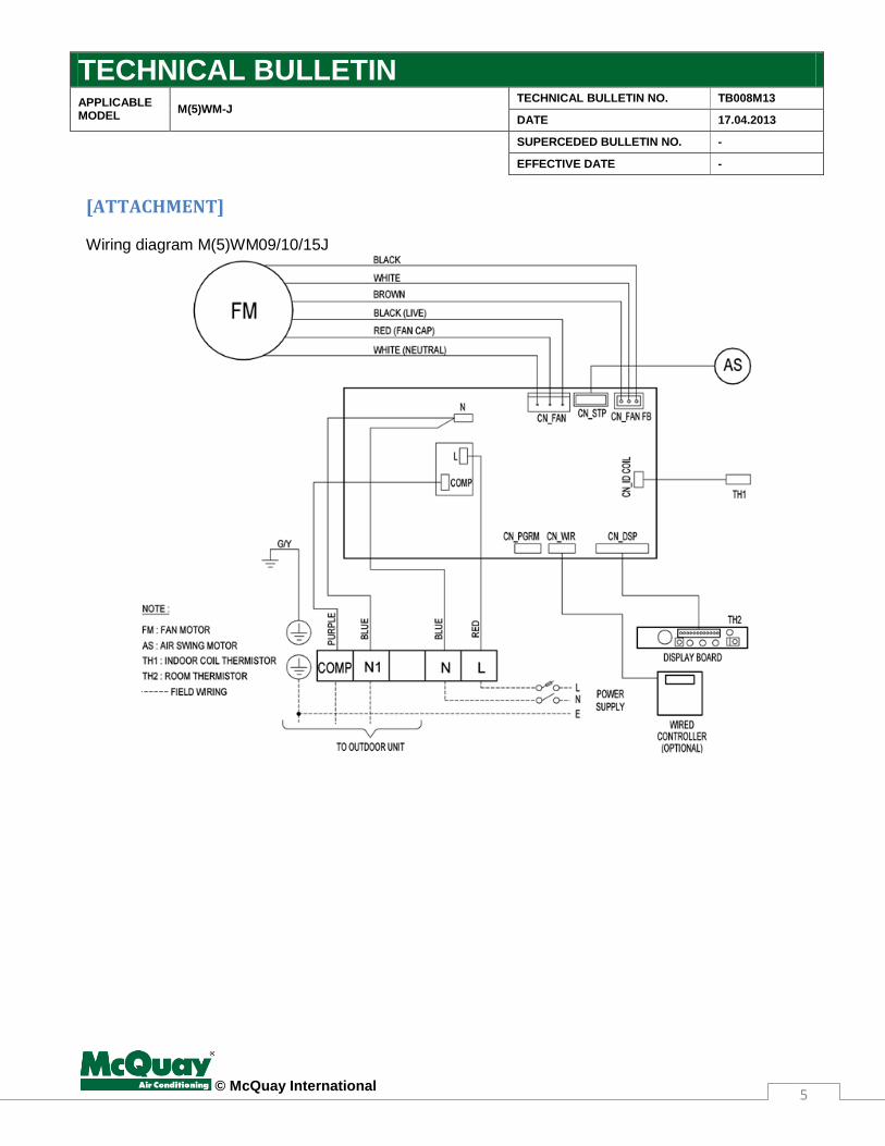
[ATTACHMENT] Wiring diagram M(5)WM09/10/15J

TECHNICAL BULLETIN APPLICABLE MODEL
M(5)WM-J TECHNICAL BULLETIN NO. TB008M13
DATE 17.04.2013
SUPERCEDED BULLETIN NO. -
EFFECTIVE DATE -
© McQuay International 6
Wiring diagram M(5)WM20/25J
TECHNICAL BULLETIN APPLICABLE MODEL
M(5)WM-J TECHNICAL BULLETIN NO. TB008M13
DATE 17.04.2013
SUPERCEDED BULLETIN NO. -
EFFECTIVE DATE -
© McQuay International 7
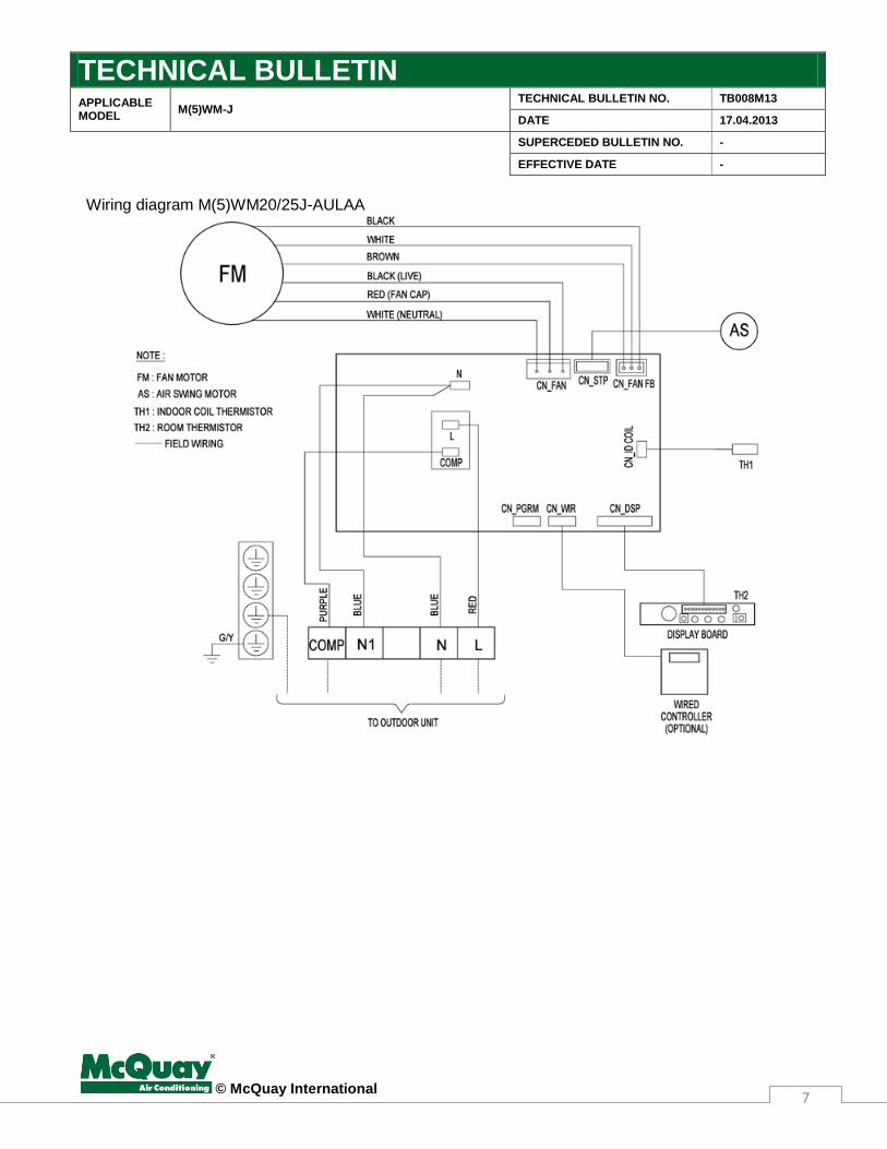
Wiring diagram M(5)WM20/25J-AULAA