
Technical Benefits and Difficulties B. Carlson July 31, 2007.
21
Technical Benefits and Difficulties B. Carlson N atio n al R esearch C ouncil C anada C o n se il n atio n a l d e rech erches C anada July 31, 2007
-
Upload
ethan-kelly -
Category
Documents
-
view
213 -
download
0
Transcript of Technical Benefits and Difficulties B. Carlson July 31, 2007.
Technical Benefits and DifficultiesB. Carlson
N ational R esearch C ounci lC anada
C onsei l national de recherchesC anada July 31, 2007
B. Carlson, 2007-Jul 31 Technical benefits and difficulties 2
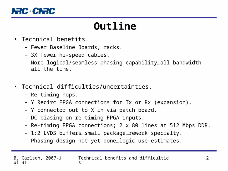
Outline• Technical benefits.
– Fewer Baseline Boards, racks.
– 3X fewer hi-speed cables.
– More logical/seamless phasing capability…all bandwidth all the time.
• Technical difficulties/uncertainties.– Re-timing hops.
– Y Recirc FPGA connections for Tx or Rx (expansion).
– Y connector out to X in via patch board.
– DC biasing on re-timing FPGA inputs.
– Re-timing FPGA connections; 2 x 80 lines at 512 Mbps DDR.
– 1:2 LVDS buffers…small package…rework specialty.
– Phasing design not yet done…logic use estimates.
B. Carlson, 2007-Jul 31 Technical benefits and difficulties 3
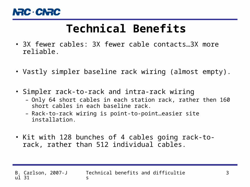
Technical Benefits• 3X fewer cables: 3X fewer cable contacts…3X more reliable.
• Vastly simpler baseline rack wiring (almost empty).
• Simpler rack-to-rack and intra-rack wiring– Only 64 short cables in each station rack, rather then 160 short cables
in each baseline rack.– Rack-to-rack wiring is point-to-point…easier site installation.
• Kit with 128 bunches of 4 cables going rack-to-rack, rather than 512 individual cables.
B. Carlson, 2007-Jul 31 Technical benefits and difficulties 4
B. Carlson, 2007-Jul 31 Technical benefits and difficulties 5
Technical Benefits
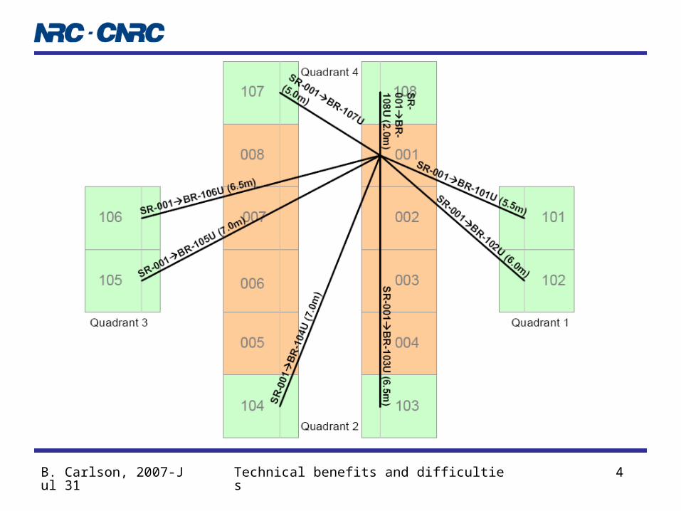
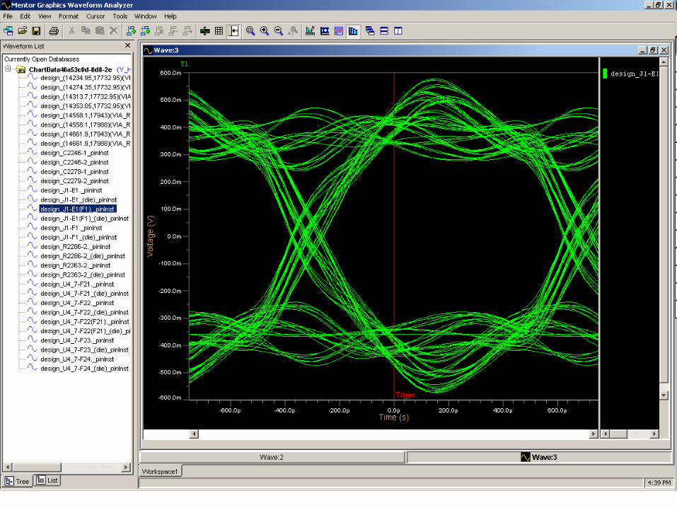
• Maximum cable length is now 7 m…better eye at the receiving end.
• Station Board outputs have to drive only 1 m of cable. X-bar board drives long cable with high-voltage PECL drivers.
• Reduces the number of baseline racks from 16 to 8…more room in correlator room for other equipment/expansion.
• Reduces the number of Baseline Boards from 160 to 128…more reliable system.
B. Carlson, 2007-Jul 31 Technical benefits and difficulties 6
Technical Benefits
• More logically consistent and dynamically available phasing…several options for getting data to VLBI recording equipment.– VLBI recording equipment can sit in racks beside baseline racks…or
elsewhere, depending on interface.
– Connect all streams into Station Board(s) that, via VSI-H output, goes to VLBI recorder (or iBob board to 10 GigE) (previous talk for details).
B. Carlson, 2007-Jul 31 Technical benefits and difficulties 7
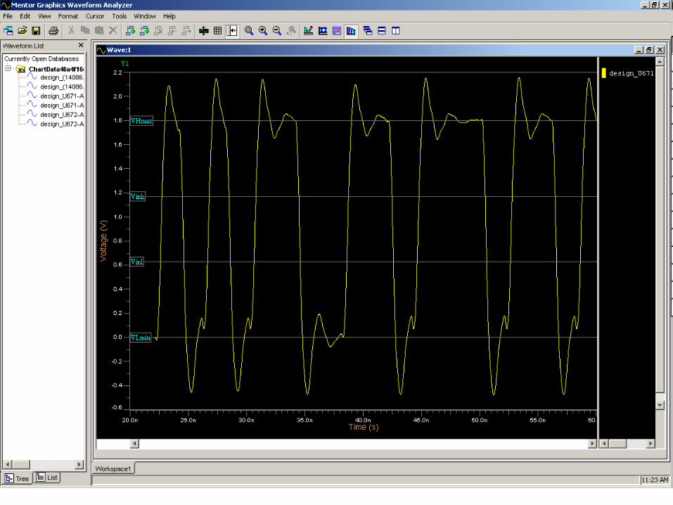
Technical diff/uncertainties
• Starting at the Station Board, there are 5 “hops”/re-timings of the signal before it gets to the last Recirc FPGA on the 2nd Baseline Board.– Low-level worry this might be a problem…you never know!
– FPGA PLLs perform very well…currently testing 3 hops under worse conditions (longer cables between hops) than in the new scheme.
– FPGA PLLs set for low bandwidth, max jitter rejection. 128 MHz clock jitter accumulation low compared to 1 Gbps anyway.
– Backup plan:• Provide external clock input to each Station and Baseline Board via blind-mate
SMA connector at the rear of the board.
• If clock jitter becomes a problem when the whole system is together, could reasonably easily add external clock network by adding SMA bulkheads, splitter, amplifier…take more work to make it fault-tolerant redundant (that’s why we dropped doing this in the first place).
B. Carlson, 2007-Jul 31 Technical benefits and difficulties 8
• The Y Recirc FPGAs have 1 Gbps Tx and Rx pins tied together on the outer layer of the PCB to allow for expansion:– Normally operate as a transmitter…so the Rx pins to Hi-z receiver in
the FPGA are a stub (~1”, including PCB, FPGA ~350 psec RT)– When operated as a receiver (expansion), the Tx pins to Hi-z
transmitter in the FPGA are a stub (~0.5”, including PCB, FPGA ~175 psec RT)
– Could be signal integrity problem (round-trip is ~350 psec).– Signal integrity on routed board with IS_analyzer...– If a problem, 1 board will work anyway; could cut traces to make 2
boards work…replace Tx/Rx connections with 0201 resistor pads in next proto round if necessary. Install resistors to use receivers for expansion.
Technical diff/uncertainties
B. Carlson, 2007-Jul 31 Technical benefits and difficulties 9
B. Carlson, 2007-Jul 31 Technical benefits and difficulties 10

B. Carlson, 2007-Jul 31 Technical benefits and difficulties 11
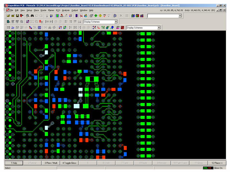
• Y connector out to X in (next board) via patch board.– Plugs into the Y connector and the X connector of the next board.
– Routes 1 Gbps LVDS signals from Y Recirc FPGAs to next board’s re-timing FPGAs max ~19” FR-4 + 2 connectors.
– Use “HyperTransport” output, ~1.6X the output voltage swing (1.2 V differential). Compatible with LVDS on the input.
– Worst case, replace with cable (~8X cost), or better PCB material (?? cost). Use largest traces possible. Use equalization on patch board?
– 28 layers, 14 routing, 14 GND, 128 diff pairs, ~10 diff pairs per layer…should be ok.
– Y7 output routed to X0 input…reorganize with the re-timing FPGA X-bar switch.
Technical diff/uncertainties

B. Carlson, 2007-Jul 31 Technical benefits and difficulties 12
Y out
X in
Y out
X inCables in
fromstationrack
unus
ed
~1.25” wide
B. Carlson, 2007-Jul 31 Technical benefits and difficulties 13
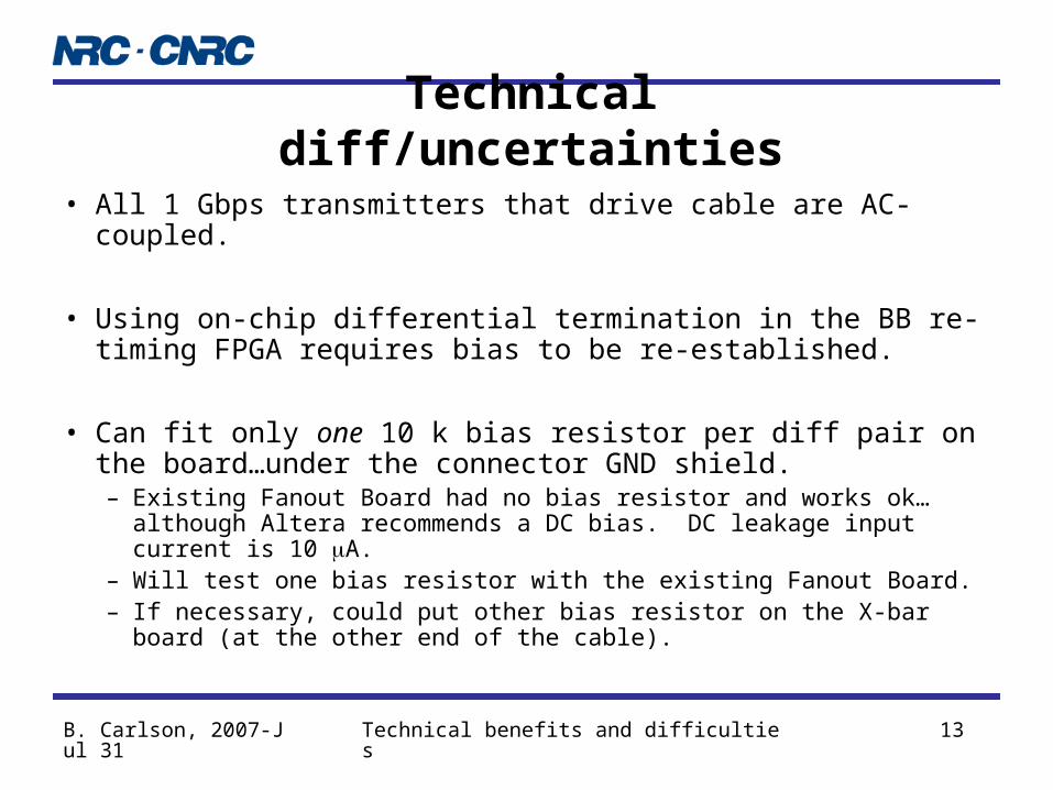
• All 1 Gbps transmitters that drive cable are AC-coupled.
• Using on-chip differential termination in the BB re-timing FPGA requires bias to be re-established.
• Can fit only one 10 k bias resistor per diff pair on the board…under the connector GND shield.– Existing Fanout Board had no bias resistor and works ok…although
Altera recommends a DC bias. DC leakage input current is 10 A.– Will test one bias resistor with the existing Fanout Board.– If necessary, could put other bias resistor on the X-bar board (at the
other end of the cable).
Technical diff/uncertainties
B. Carlson, 2007-Jul 31 Technical benefits and difficulties 14
B. Carlson, 2007-Jul 31 Technical benefits and difficulties 15
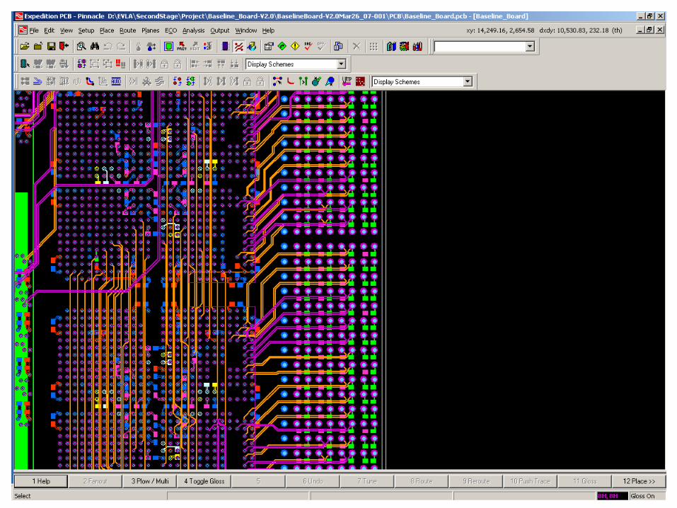
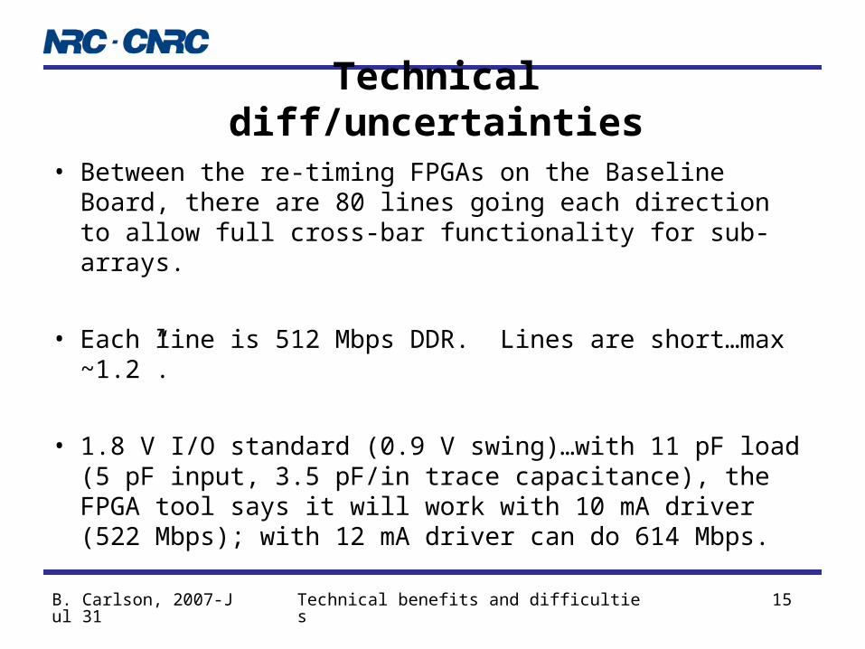
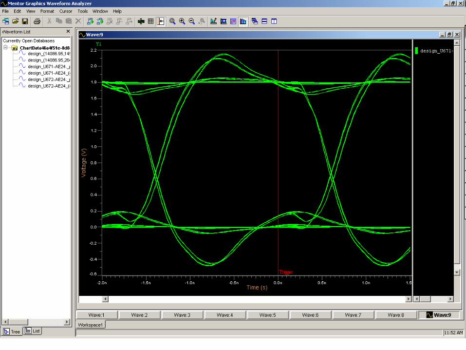
• Between the re-timing FPGAs on the Baseline Board, there are 80 lines going each direction to allow full cross-bar functionality for sub-arrays.
• Each line is 512 Mbps DDR. Lines are short…max ~1.2”.
• 1.8 V I/O standard (0.9 V swing)…with 11 pF load (5 pF input, 3.5 pF/in trace capacitance), the FPGA tool says it will work with 10 mA driver (522 Mbps); with 12 mA driver can do 614 Mbps.
Technical diff/uncertainties
B. Carlson, 2007-Jul 31 Technical benefits and difficulties 16
B. Carlson, 2007-Jul 31 Technical benefits and difficulties 17
B. Carlson, 2007-Jul 31 Technical benefits and difficulties 18
• 1:2 LVDS fanout buffers after the re-timing FPGAs are in 2 mm x 2 mm package.
• Re-work requires special techniques…use the BGA rework machine, but not the pickup nozzle.
• Requires some additional learning…need to operate the BGA reflow head in manual mode…needs investigation/training.
Technical diff/uncertainties
B. Carlson, 2007-Jul 31 Technical benefits and difficulties 19
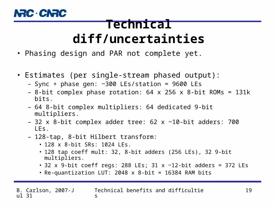
• Phasing design and PAR not complete yet.
• Estimates (per single-stream phased output):– Sync + phase gen: ~300 LEs/station = 9600 LEs– 8-bit complex phase rotation: 64 x 256 x 8-bit ROMs = 131k bits.– 64 8-bit complex multipliers: 64 dedicated 9-bit multipliers.– 32 x 8-bit complex adder tree: 62 x ~10-bit adders: 700 LEs.– 128-tap, 8-bit Hilbert transform:
• 128 x 8-bit SRs: 1024 LEs.• 128 tap coeff mult: 32, 8-bit adders (256 LEs), 32 9-bit multipliers.• 32 x 9-bit coeff regs: 288 LEs; 31 x ~12-bit adders = 372 LEs• Re-quantization LUT: 2048 x 8-bit = 16384 RAM bits
Technical diff/uncertainties

B. Carlson, 2007-Jul 31 Technical benefits and difficulties 20
• Single-stream phasing estimates (1 phased output):– 12,224 LEs, 96 x 9-bit multipliers, 200k RAM bits.
• The re-timing/Xbar requires 12k LEs, 0 RAM, 0 multipliers.
• The EP2S60 chip has ~48 k LEs, 288 9-bit multipliers, 2.5 Mbits RAM.
• With only one phased output per chip, use ~50% LEs, 33% of the multipliers, and 8% of the RAM.– Seems like each S60 chip might do 2 phased outputs…therefore 4
sub-arrays/sub-band. Or, S30 for 2 sub-arrays per sub-band??
Technical diff/uncertainties
B. Carlson, 2007-Jul 31 Technical benefits and difficulties 21
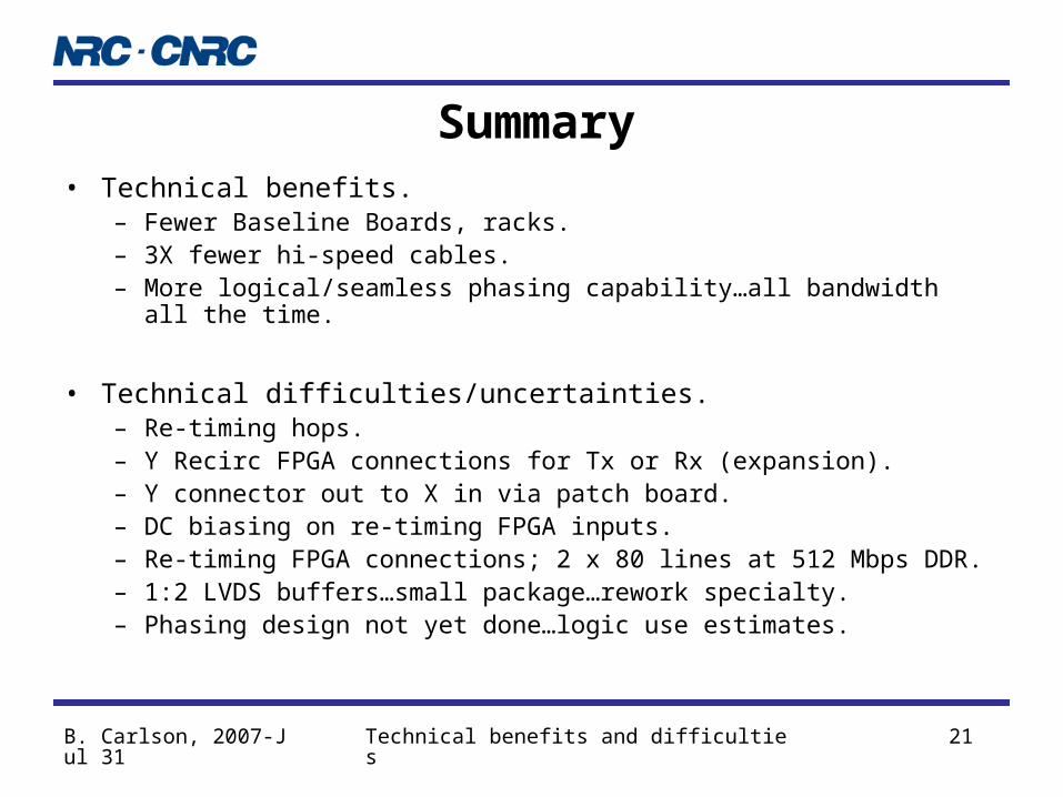
Summary• Technical benefits.
– Fewer Baseline Boards, racks.– 3X fewer hi-speed cables.– More logical/seamless phasing capability…all bandwidth all the time.
• Technical difficulties/uncertainties.– Re-timing hops.– Y Recirc FPGA connections for Tx or Rx (expansion).– Y connector out to X in via patch board.– DC biasing on re-timing FPGA inputs.– Re-timing FPGA connections; 2 x 80 lines at 512 Mbps DDR.– 1:2 LVDS buffers…small package…rework specialty.– Phasing design not yet done…logic use estimates.