team2 PT2009X firstdraft - University of Texas at San...
40
PT2009X Team #2 Submitted by: Emiliano Morales Rebecca Conner Christopher Montanez Mario Espinoza Submitted to: August Allo University of Texas at San Antonio Department of Electrical and Computer Engineering 1 UTSA Circle, San Antonio, TX. 78249
Transcript of team2 PT2009X firstdraft - University of Texas at San...

PT2009X Team #2
Submitted by:
Emiliano Morales
Rebecca Conner
Christopher Montanez
Mario Espinoza
Submitted to:
August Allo
University of Texas at San Antonio
Department of Electrical and Computer Engineering
1 UTSA Circle, San Antonio, TX. 78249

Date:
Contents
1.0 Executive Summary ........................................................................................................................ 5
2.0 Introduction ..................................................................................................................................... 5
3.0 Need for Design ............................................................................................................................... 5
4.0 Literature and patent search results ............................................................................................. 6
5.0 Marketing Analysis and Market Strategy .................................................................................... 6
5.1 Market Analysis Summary ........................................................................................................ 6
5.2 Market Segmentation ................................................................................................................. 7
6.0 Engineering Design Constraints .................................................................................................... 7
6.1 Global Design Constraints .......................................................................................................... 7
6.2 Local Design Constraints ............................................................................................................ 8
7.0 User Requirements .......................................................................................................................... 9
7.1 User Requirements ...................................................................................................................... 9
7.2 System Requirements ................................................................................................................. 9
7.3 Interface Requirements ............................................................................................................ 10
8.0 Engineering Codes and Standards .............................................................................................. 10
9.0 Design Concepts ............................................................................................................................ 10
9.1 System 1 ..................................................................................................................................... 11
9.2 System 2 ..................................................................................................................................... 11
9.3 System 3 ..................................................................................................................................... 11
9.4 Pugh Matrix and Results .......................................................................................................... 12
10.0 High Level Block Diagram ........................................................................................................... 13
11.0 Major Components ....................................................................................................................... 13
11.1 Spartan 3-E Starter Board ....................................................................................................... 14
11.2 Muxes ......................................................................................................................................... 14

11.3 LED Strip ................................................................................................................................... 14
12.0 Detailed Design .............................................................................................................................. 15
12.1 Hardware ...................................................................................... Error! Bookmark not defined.
12.2 Software ..................................................................................................................................... 20
12.3 Engineering Analysis and Calculations ................................................................................... 33
13.0 Major Problems ............................................................................................................................ 34
13.1 FPGA Glitches ........................................................................................................................... 34
13.2 Latched Mux Fix ....................................................................................................................... 34
13.3 Other Problems ............................................................................ Error! Bookmark not defined.
14.0 Integration and Implementation .................................................................................................. 35
15.0 Comments and Conclusion ........................................................................................................... 37
16.0 Team Members .............................................................................................................................. 37
16.1 Emiliano Morales ...................................................................................................................... 37
16.2 Rebecca Conner ........................................................................................................................ 38
16.3 Christopher Montanez .............................................................................................................. 38
16.4 Mario Espinoza ......................................................................................................................... 39
17.0 References ...................................................................................................................................... 40

1.0 Executive Summary
We changed the project. We prevailed… TBC
2.0 Introduction
Piano is a common and widely known instrument, yet the market for pianos and
keyboards is not as popular as guitars or other instruments. Video games such as the Guitar
Hero Series, Rockband Series, DJ Hero, and popular learning software such as Guitar Pro
primarily target guitar and drum enthusiasts. The software and game markets for pianos and
keyboards is limited in comparison.
PT2009X, which stands for “Piano Teacher 2009X”, promises to deliver a fun and
effective way to hone an amateur’s keyboarding skills. This is accomplished by using
indicator LED’s that will indicate which notes to be pressed, in conjunction with a graphical
display. The graphical display will also have an indicator as to which note is to be played
next. PT2009X also offers a different and faster method of associating key notation with the
piano keys as opposed to the rote learning of melodies. The user will learn the melody while
getting them familiarized with note reading efficiently rather than learning a melody by
mechanically repeating it. The PT2009X will include learning modules and lessons and
drills. The PT2009X will accomplish its goal only with keyboards that come equipped with
MIDI-OUT ports. The note that result from pressing the keys will be derived via the MIDI-
out port, which will then be used by a FPGA which will determine the performance and
power the graphical display.
3.0 Need for Design
There are three major needs for this design. The first the need is need for a conventional
and entertaining method of improving one’s keyboarding skills. Second, the PT2009X
addresses the need for portability and flexibility which other systems fail to offer. As other
systems fail to address, there will be no computer or computer software necessary to process
performance, all will be accomplished via the FPGA. The financial obligations of a tutor will
be eliminated. Finally, this is a system to buy for keyboards and pianos (equipped with
MIDI-Out ports) that do not have a learning mechanism integrated in them. It eliminates the

need of having to buy an entirely new keyboard that has blinking keys or some other sort of
learning mechanism, the user can implement the PT2009X to the keyboard they already own
and are comfortable with.
4.0 Literature and patent search results
There was one particular article in PDF format found on the internet that was very helpful
at underlining how MIDI works. The article, called "MIDI BASICS", introduced the need for
a universal asynchronous receiver/transmitter (UART) and also clearly described what a
MIDI signal looks like. Another valuable source was a book called "FPGA Prototyping by
VHDL Examples: Xilinx Spartan-3 Version" by Pong P. Chu. This book helped the team
review VHDL programming and was extensively useful for the display and UART
implementation.
There are several patents that employ the use of MIDI to teach piano. The most related to
the PT2009X include: Patent No. US 6751439 B2, Patent No. US 7174510 B2, and Patent
No. US 6211451 B2. The first patent involves the need for a teacher to monitor progress of a
student via a network, which PT2009X eliminates. The second one is about the same
concept, but does not use LED's to indicate which note to be played. Instead, a picture of the
keyboard is displayed through via a monitor. The last one also requires the use of a network
with a supervisory computer to evaluate performance. What is uniquely distinct of PT2009X
from the described patents is that the PT2009X does not require the use of a personal
computer nor computer software programs to operate.
5.0 Marketing Analysis and Market Strategy
5.1 Market Analysis Summary
Through an extensive internet research, only one product similar to the PT2009X exists.
It consists of LED stickers that are adhered to the keys and light up as each key is required to
be pressed. This design lacked a graphical display. PT2009X appeals to anyone who is
willing to perfect their skills since it provides a key element not found in many training
systems, fun. The way PT2009X is set up is somewhat like the notorious Guitar Hero video
game in which the user has to press the keys to progress satisfactorily through the song. The
more keys pressed at the correct timing, the more achievements the user receives. PT2009X

works under the same concept, except it is applied to an actual instrument for the benefit of
learning the real melody. This should attract those who are willing to become better at piano.
5.2 Market Segmentation
The segmentation of the market can be broken down into three major sectors:
1) Book publishers who might be interested in supplementing the PT2009X with
exclusive manuals, lectures, and drills to accompany the system.
2) Music training schools who wish to have a method of personalizing large classes.
This system should be able to target the individual weaknesses of the user.
3) The general consumer who wish to hone their keyboarding skills or explore a new
method of practicing.
6.0 Engineering Design Constraints
6.1 Global Design Constraints
Economic Factors- No
Potential risks on sales will not occur unless another cheap design emerges.
Environmental Factors- Yes
Improper disposal of circuit board and rubber strip could cause environmental
harm.
Sustainability- Yes
The sustainability of our design on the market will depend on the fluctuating
economy.
Manufacturability- No
It can be manufactured locally or globally effectively.
Ethical Consideration- No

The design does not promote anything unethical.
Health and Safety- Yes
Circuit board and rubber disposal may cause minor health issues. The flashing
LEDs could cause health problems to individuals with certain disorders.
Social Ramifications- No
Our product does not raise any social issues.
Political Factors- No
The design will not impact any political sector.
Legal Issues- Yes
It may depend on the copyrights of a musical piece.
6.2 Local Design Constraints
Cost- Yes
As students, our budget to design the project is finite.
Schedule- Yes
As graduating senior students, our design must be finalized by the end of
November 2009.
Manufacturability- No
The design doesn’t require anything more complex than soldering and
programming FPGAs.
Ethical Considerations- No
At this point, there are no apparent ethical issues.
Health and Safety Issues- Yes
Health and safety issues can become an issue during prototyping, particularly lab
injuries related to the amount of soldering needed.
Legal- Yes
Since prototyping of our design include some safety issues a legal constraint may
exist.
7.0 User Requirements
Below is a list of the user and system requirements of the PT2009X. The most prevalent
ones include the requirement of the system to successfully read MIDI signals determine
whether a note has been struck or missed. The most important requirement for the user is that
the user’s keyboard or piano must have a MIDI-Out port, else the system won’t be
operational. The complete list is below:
7.1 User Requirements
The device must be user friendly.
The device must be able to accurately display music notes.
The device must be able to accurately display correct key position on LED strip.
User must have MIDI capable keyboard.
Device must be able to start when user is ready.
User must have the ability to increase or decrease the tempo.
User must have the ability to see their performance.
7.2 System Requirements
The system must be able to display notes to pre-programmed melodies.
The LEDs must light up to indicate correct piano key to be played.
The system must light up LEDs in sync with the music being displayed.
The system must be able to indicate the amount of notes hit and missed.
The system must be able to be mounted onto a keyboard with ease.
The system must be able to receive feedback from the keyboard.

The system must have preprogrammed music.
The system must be able to extract specific bits from MIDI output.
The system must be able to encode the signal to the LED strip.
The system must be capable of lighting up several LEDs simultaneously.
7.3 Interface Requirements
Must be independent of personal computers and computer software.
Must be able to display music on a VGA monitor.
Must be able to light up LEDs when song begins.
Must interface with a MIDI capable piano keyboard.
Must be able to indicate current position in music.
The LED strip must fit comfortably above the keyboard without any obstructions.
8.0 Engineering Codes and Standards
Some of the most relevant engineering codes and standards that pertain to the safety of
the users of the PT2009X are listed below. These standards were acquired from the IEEE
Xplore Digital Library and are followed by a brief description.
1076-2008 Active- IEEE Standard VHDL Language Reference Manual.
1076-2007 Active- IEEE Standard VHDL Analog and Mixed-Signal Extensions.
1076.2-1996 Active- IEEE Standard VHDL Mathematical Packages Reaffirmed 2002
1076.3-1997 Active IEEE Standard VHDL Synthesis Packages.
9.0 Design Concepts
There are three major components that comprise the PT2009X. These include the display,
the LED strip, and the instruction processor. There are several methods to execute a graphical
display. The options were liquid crystal display (LCD) screens, television sets with AV
composite inputs, or monitors with VGA inputs. There also exist many methods to create a
LED strip which will have the LED’s mounted above each piano key. Finally, and most
importantly, there are two different ways to make the whole system operate. The two options
were using an FPGA, which uses VHDL as programming language, or a PIC microcontroller,
which uses Assembly and/or C++ programming languages. Below are the three most feasible

design alternatives using a combination of the different options of the major components
listed above.
9.1 System 1
This system uses an LCD to display the notes that need to be played and the performance
measurement of the user. This system also uses a PIC programmable microcontroller to drive
the LCD, to turn on the LED’s, and to configure the signals coming out of the MIDI-out port.
This system uses wood as the strip material to neatly mount all the LED’s on top of the
keyboard.
9.2 System 2
This second system uses a monitor with a VGA input for displaying the musical notes
and the performance. This will be accomplished by using an FPGA that uses VHDL as the
programming language. The LED strip material will be rubber-type material, which will
prove to be flexible.
9.3 System 3
This third system will use a conventional TV monitor that has AV composite inputs to
display the musical notes and the performance of the user. The display will be driven by a
FPGA and the signal coming out of the MIDI-Out port will be configured by a PIC
microcontroller. The LED strip material will be made of thick and flexible fabric texture.

9.4 Pugh Matrix and Results
Below is the Pugh Matrix table and its corresponding results.
Pugh Matrix
Design Constraint Weight System 1 System 2 System 3
Design must have a reasonable cost. 15 8.5 7 6
Design must be completed on time. 25 6 8.5 7
Design must have a friendly interface. 6 8 8 7
Design must be able to convey instructions via a graphical display. 13 5 8 8.5
The graphical display must be legible and visible. 6 4 8 8
The LED strip must fit comfortably above the keys without any noticeable
obstructions. 10 5 7 5
Design must be able to accurately determine and measure performance
and check whether the keys have been struck accordingly. 6 8 9 8
User must be able to navigate through menus. 5 7 9 9
Design must be able to communicate with the MIDI signal of keyboard. 8 6 9 6
The device must have a tunable tempo to increase or decrease the piece
of melody. 6 6 9 9
Total 100 631.5 812.5 710.5
The clear winner is system two, which uses a monitor for display, an FPGA to run the
system, and rubber as the material for the LED strip. Massive points were awarded by the
second constraint, which is getting the design done on time. As engineering students at
UTSA, the team has received enough exposure to both VHDL and C++, however there was
not enough reference material found for writing code for the display and the UART in C++.
The book, “FPGA Prototyping by VHDL Examples: Xilinx Spartan-3 Version" by Pong P.
Chu had substantial information on UART and graphical displays, hence the team decided to
concentrate on VHDL. The wood strip would have worked well on the design, however the
construction of the strip would consume a lot of time. A monitor proved to be the most
suitable means of display for the design, due primarily to the fact that the book also provided

detailed information on how to display to monitors via VGA ports. The LCD would have
proved to be less legible since the space is limited on LCD screen, and a bigger LCD would
have cost considerably more. Monitors provide more pixels, which would be essential to
provide the user with a much clear picture of the staff and the position of the notes within the
staff.
10.0 High Level Block Diagram
Figure 1 ‐ High level block diagram.
11.0 Major Components
The PT2009X can be broken down into four major sections, the display of the music,
configuring signals from the keyboard, timing and performance measurement, and the

powering of the LED’s. Of these sections, the three major components that make the
PT2009X function are the FPGA, the decoder, and the LED strip.
11.1 Spartan 3-E Starter Board
This is where the Field-Programmable Gate Array (FPGA) resides. The FPGA is the
heart of the PT2009X. It is what deciphers the signal that is coming from the keyboard,
through the use of a universal asynchronous receiver/ transmitter (UART), and it is what will
turn the LED’s on and off. It is also what drives the display and keeps track of the user’s
performance by logging the hits and misses of the notes. The Spartan 3-E development board
has 500k gates and comes with a 32-bit RISC processor. It was chosen because of its superior
ability to manipulate timing over a conventional microcontroller and it was chosen over the
inferior BASYS FPGA board. The price was also a major factor in selecting this board over
the superior Spartan 3E-1600 development board, which was priced at $225.00 minus
applicable handling and taxes.
11.2 Muxes
The system of multiplexers is the gateway from the board to the LED strip. The design
needed a way to use seven bits from the board and to determine which of seventy-six LEDs
to illuminate. There is essentially only one way to implement this, but different methods were
researched, including using a crossbar switch, but the most efficient way to decipher the
information was to use a decoder circuit consisting of multiplexers. The crossbar method
involved complex wiring which would have been difficult to troubleshoot if a mistake were
made or a wire became loose. Not having much experience working with and purchasing
actual digital components, generic multiplexers were chosen to be used to implement the
encoder circuit. The M74HC238, 3 to 8 multiplexer, was used for the first level of the
decoder and the MM74HC4514, 4 to 16 multiplexer, was used for the second level of the
decoder.
11.3 LED Strip

For this project several key aspects were considered when it came to determining the
most feasible implementation of the LED Strip. For the development of this component,
several key aspects came into consideration, which include luminosity, physical dimensions,
wavelength, current and voltage parameters, and limitations of availability and cost. The base
of the strip consists of a vinyl based material which provides flexibility and the ease of
workmanship. Other materials which were considered were wood, fabric texture, and
Plexiglas. Although these materials are manageable, they presented diverse constraints and
aesthetic limitations. The rigidness of the material was also taken into consideration, the
possibility of damaging the instrument could prove catastrophic. Selecting the LEDS
involved a bit more consideration, since the decoders provided current limitations. When it
came to selecting the wavelength of the LED’s, energy conservation was a factor in the
decision, resulting in the following colors; High Efficiency Red and High Efficiency Green,
these colors also are widely available. Other colors that were considered were ultra-violet and
ultra-red. Both involved more energy consumption and were more expensive. To connect the
seventy-six LED’s three segments of ribbon wire was utilized. This provided a manageable
and structured way of connecting the strip to the decoder circuit. The possibility of creating
an additional circuit to route the signals through fewer channels was explored but it elevated
the costs, and involved another sector of design. Implementation and troubleshooting of a
new sector would conflict with the time constraint as well as with the restricted budget.
12.0 Detailed Design
The design relied heavily on programming the FPGA. The hardware components of
the PT2009X include the LED strip, the decoder tree, and the MIDI to FPGA interfacing
circuit. The software design section can be broken down into several modules:
1) UART 2) Note timing, synchronization, and detection 3) Tempo control 4) VGA
synchronization 5) Static graphics 6) Text.
12.1 Hardware
12.1.1 LEDs

Mario was given the task to research the LED interface, which involved researching a
multiplexing design that would convert an seven bit parallel port input coming from the
FPGA to seventy-six possible LED positions. He was also given the task of researching
the parts and key components of such element. Once the components and their respective
electrical characteristics were selected, he was assigned to construct the LED strip, which
involved the craftsmanship of soldering 76 LED’s with dimensional bounds as well as the
color sequence layout restrictions. The LEDs and mounts where added to the platform to
give a more aesthetic and seamless design. Mario was also responsible for the drilling of
76 holes and the installation of a cylindrical base for the each LED as well as their
respective LED apron. The strip was also trimmed to ensure the display of the keyboard
buttons and reduce obstruction, the need to secure the wiring was solved using adhesive
to secure each LED wire.
12.1.2 MIDI to FPGA interface
Emiliano’s sole priority for this design was to receive and decode the MIDI signal
coming out of the piano keyboard and clean the signal of all unnecessary information.
The first step towards this process was connecting the output of the MIDI port to an
oscilloscope and analyzing the signal. According to research conducted, the MIDI DIN
180º connector has 5 pins, two of which are unused. This was decided this way, because
at the time before standardizing MIDI, the 5 pin DIN 180 º connector was cheaper to
produce. The middle pin is ground and the remaining two pins, when connected, form a
closed loop where the signal propagates. When the team connected the output of the
MIDI port to the oscilloscope, no signal was received when pressing the keys of the piano
keyboard. After researching the causes for this, the team stumbled upon the solution on a
website that described a MIDI-to-Microcontroller interface. The interface circuit called
for an opto-isolator. An opto-isolator is basically an LED and a photo-transistor packed
together.

GND_0
0
6N138
2
3
5
6
8
7
MIDI Input
1
2
3
4
5
1N914
12
220270
VCC
To FPGA
Figure 2 ‐ MIDI to FPGA interface UART.
The 6N138 shown in Figure 2 is the opto-isolator circuit. The LED and the photo-
transistor separate the signal to ensure protection. After this configuration was applied,
the signal going into the FPGA was readable.
12.1.3 Decoder Tree
Rebecca’s interest in digital system design made her ideal to design, implement, and
test the decoder circuit. The design required illuminating 76 LEDs based on the output, a
7 bit code, from the board. Given the requirements of the design there was essentially
only one way of implementing this portion of the design, and that is with the use of a
decoder circuit. To decode 7 inputs to 76 outputs, two levels of multiplexers were
needed. As Figure 6 illustrates, the first level consisted of a 3 to 8 multiplexer, taking the
three most significant bits as inputs, Figures 3 and 4 show the pin layout and truth table
for this component. The output of the first level determined which of the 4 to 16
multiplexers, which make up the 2nd level of multiplexers, to enable, the pin layout and
truth table for this component is illustrated in Figure 5. To illuminate all 76 LEDs, 5
multiplexers had to be used for the 2nd level of logic. The LEDs are connected to the
output of 2nd level of multiplexers, which use the remaining 4 lower bits to decipher
which LED to illuminate. Figure 6 illustrates the schematic of the decoder tree.

Figure 3 ‐ 3 to 8 Multiplexor pin diagram.
Figure 4 ‐ 3 to 8 Multiplexor truth table.

Figure 5 ‐ Pin layout and truth table for 4 to 16 multiplexors.

Figure 6 ‐ Multiplexing scheme for to use 7 inputs to control 76 discrete LEDs.
12.2 Software
12.2.1 UART
Emiliano was in charge of receiving the signal from the MIDI out port and decoding
it for use by the FPGA. A universal asynchronous receiver/transmitter (UART) was
needed to decode the signal coming out the piano keyboard. The UART’s function was
constructed from code found in the FPGA Prototyping by VHDL Examples book. Some

modifications were done to the code in order for it to work according to the design’s
need. The preceding image shows the overall block diagram of the code constructed to
decipher the MIDI signal.
Figure 7 ‐ Block diagram of VHDL code to decode MIDI signal.
The goal of the code was to receive the signal from the keyboard and filter all the excess
information (such as status bytes, velocity bytes, etc). A sample signal byte would
generated by the keyboard would look like in figure 8. It consists of a start bit and an end
bit. The information is conveyed in the middle eight bits and this occurs at a rate of
31,250 bits per second. The job of the signal receiver can be broken down into simple
steps. First, it the receiver checks for a ‘0’, or a high signal. Once detected, it starts taking
“ticks” from the baud generator. The ticks occur periodically such that there are 16 ticks
per bit. When the start bit is detected, the tick counter begins and so does the process. The
first time,
only seven
ticks are
counted, if
signal is still
high, then it
restarts the counter. The counter then counts sixteen more times, records the bit in an
array, and restarts the counter. This occurs eight times (equivalent to one byte). The final
time it counts a last sixteen times just to make sure the stop bit is received. If all is okay,
Figure 8 ‐ A sample signal byte generated from the keyboard.

then the stored array is outputted to the next phase, the Buffer state. According to the
author of the code, the buffer helps prevent a signal from being read twice. After a byte
leaves the buffer, it enters the filter stage. In this stage, the “excess” bytes are filtered.
Excess bytes are considered those that are not bytes that indicate the key press, but status
bytes or bytes that describe the velocity at which the key was stroked. Figure 9 shows a
sample of what the signal looks like before it is filtered when the Middle C and C# are
pressed at the same time. This was taken with the use of PICKit2’s UART Tool.
Figure 9 ‐ Sample of unfiltered output when Middle C and C# are pressed in unison.
The most common bytes (in hex) “F8” and “FE” are system bytes that are periodically
flowing from the port, even when nothing is being played. The byte “90” indicates the
message “Note On”. Following that is the byte “3D” in the blue box, this corresponds the
C#. Followed by byte “3B” which is indicative of the velocity it has been hit. One cycle
and the next byte on the blue box is “3C” indicative of the Middle C note and followed
by the green box which indicates the velocity. After several cycles, the notes are

displayed again followed by byte “00”,which is an indication that the note has been
released. The next step after receiving the signal was to write the code to filter it. All the
unnecessary bytes such as the common system bytes, the “Note On” bytes, the “Velocity”
bytes and the “Note Off” bytes needed to be filtered so that false readings would not enter
the main code.
Figure 10 shows the state diagram of the filter code. First, the data incoming the from
the buffer to the filter is checked to determine if it is a status byte. Since all status bytes
have a most significant bit of 1, it becomes easy to determine that anything less than
“1000000” in binary is not a status byte.
YES
NO
Figure 10 ‐ State diagram for MIDI filter code.
The incoming data is then stored into a vector. Next, the state waits for the next incoming
bit. Once the next bit arrives, it is stored into the “next_byte” vector. This vector will be
used for comparison on the next state. If the “next_byte” is equal to zero, that means that

the byte before that is being released and that the process should be ignored and continue.
This will allow for the filter to filter to only output a signal when the byte is followed by
a velocity byte, and not again when it is released.
The Baud Generator unit, the UART Signal Receiver unit, and the Buffer unit were
modified from the code provided on chapter 7 of the FPGA Prototyping by VHDL
Examples book. To make the code a bit more compact, the UART transmit code was
discarded as well as other signal that were tied to constants. The default baud rate was
recalculated. The Filter unit was generated by Emiliano from concepts learned in the
book.
12.2.2 Note Timing and Synchronization
The note timing unit's main purpose, based on an incoming tempo and keyboard midi
output, is to start the game when the first note is played, output the current note which is
to be shown on the screen, select the correct pattern to display on the LED strip, and
update hit and miss counters. An overview of the inputs and outputs of the note timing
unit is displayed in figure 11.
Figure 11 - Overview of the inputs and outputs of the note tracking unit.
The song chosen for this particular project contains notes that were all equally spaced
apart, rhythmically. Because of this fact, the timing problem was simplified by having a
timer that would advance to the next note. This timer is controlled by the 32-bit tempo
vector coming in from the tempo unit.
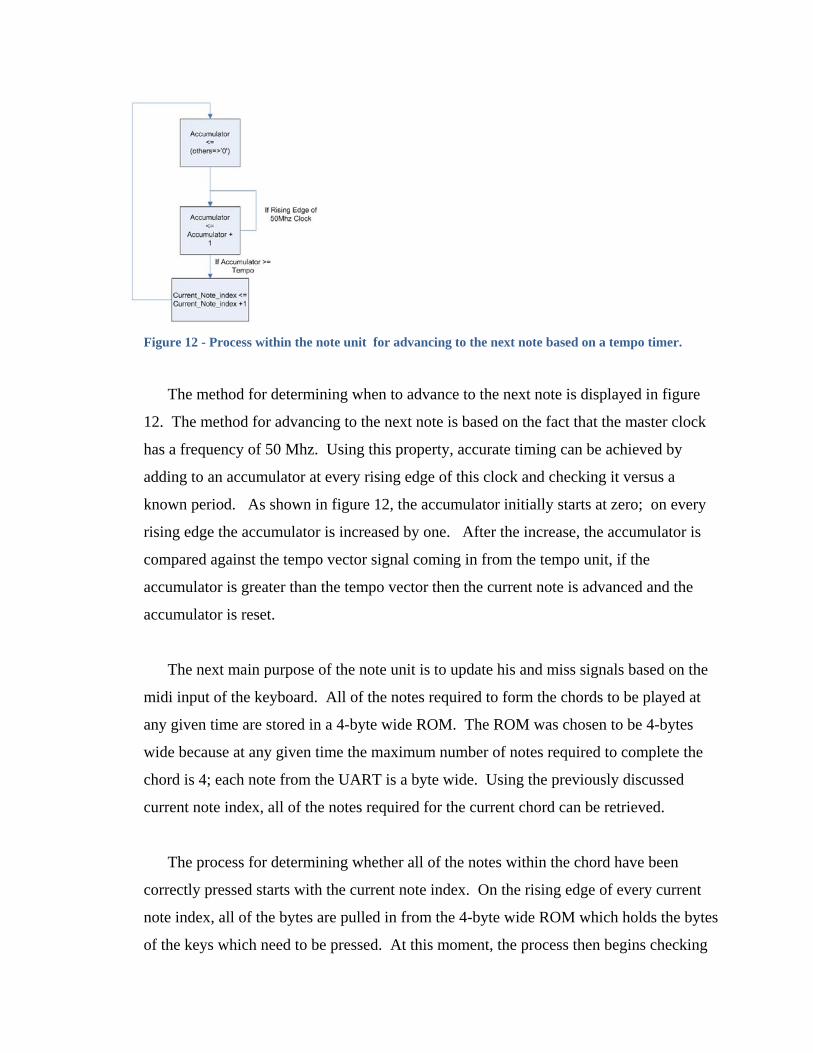
Figure 12 - Process within the note unit for advancing to the next note based on a tempo timer.
The method for determining when to advance to the next note is displayed in figure
12. The method for advancing to the next note is based on the fact that the master clock
has a frequency of 50 Mhz. Using this property, accurate timing can be achieved by
adding to an accumulator at every rising edge of this clock and checking it versus a
known period. As shown in figure 12, the accumulator initially starts at zero; on every
rising edge the accumulator is increased by one. After the increase, the accumulator is
compared against the tempo vector signal coming in from the tempo unit, if the
accumulator is greater than the tempo vector then the current note is advanced and the
accumulator is reset.
The next main purpose of the note unit is to update his and miss signals based on the
midi input of the keyboard. All of the notes required to form the chords to be played at
any given time are stored in a 4-byte wide ROM. The ROM was chosen to be 4-bytes
wide because at any given time the maximum number of notes required to complete the
chord is 4; each note from the UART is a byte wide. Using the previously discussed
current note index, all of the notes required for the current chord can be retrieved.
The process for determining whether all of the notes within the chord have been
correctly pressed starts with the current note index. On the rising edge of every current
note index, all of the bytes are pulled in from the 4-byte wide ROM which holds the bytes
of the keys which need to be pressed. At this moment, the process then begins checking

to see if the current MIDI byte input from the UART is equal to any of the bytes required
for the chord. If the input byte is equal to any of the ROM bytes, a flag is set indicating
that that note has been 'cleared.' In order for the current chord to be considered a success,
all four flags must be set; this would indicate that all of the notes were hit.
At the beginning of the next rising edge of the current note index, the flags are
evaluated. If all of the flags are set, then a signal is output to increment the success
counter. Otherwise, if any of the flags remained low, then that means one or more of the
keys were missed; therefore, a signal to the miss counter would be set high. Finally, all
of the flags are once again cleared so that they are ready to detect whether the next chord
was correctly played.
12.2.3 Tempo Control
The Tempo Unit's purpose is to output a tempo period which is used by the note unit.
The tempo unit has three main inputs and one main output, as displayed in figure 13.
Figure 13 - Overview of the inputs and output of the tempo module.
Tempo values, or period, were stored in ROM as 32 bit unsigned vectors. The tempo
vector output is initially determined by returning a value from the ROM using a default
index. Then, as the user turns the knob either left or right, the index value will be
changed. As the index value is changed, the 32-bit unsigned tempo output vector will
immediately be changed. This vector is then used as an input to the note unit which uses
it as a period for determining when to advance to the next note.
The push button attached to the rotary knob is used as an input to return the index to
the default value; once the index goes to the default value, the tempo vector goes to the

default value. This feature allows the user, at any time during the program to push the
rotary button and have the song play at the original speed.
12.2.4 VGA Synchronization
The VGA synchronization unit is the heart of the display software. This module is
used to generate all of the signals that interact with the VGA display. The inputs and
outputs of the VGA unit are displayed in figure 14. The VGA synchronization unit
creates the image by constantly refreshing a sequence of predetermined horizontal lines.
These horizontal lines are determined by the graphics unit and text unit; these values are
then multiplexed to display the correct layering of the image on the screen.
Figure 14 - An overview of the inputs and outputs of the VGA synchronization module.
The internal oscillator's and amplifiers within the monitor create a sawtooth
waveforms to control both the horizontal and vertical location of the pixel being
displayed on the screen. These sawtooth waveforms are controlled by both the digital
hsync and vsync pulses. The rising and falling edges of the hsync and vsync signals
correspond to the rising and falling edges of the sawtooth waveform. Synchronizing the
hsync and vsync pulses allows for a specific pixel x and pixel y location on the screen at
any given time.
These pixel x and pixel y signals are then passed to the graphics and text modules.
Based on the position these modules will output the correct 3-bit RGB vector to display
the correct color. In addition more circuitry is necessary in order to correctly display the
text and graphics. Specifically a RGB multiplexing circuit was required to display the
desired layering; the multiplexing circuit used is displayed in figure 15.

Figure 15 - RGB Multiplexing circuit.
At any given time, only one 3-bit RGB vector can be output to the monitor. To
accomplish this the a multiplexing circuit was used to select the correct output RGB
vector. It was decided that text should be layered at the front, and graphics should be in
the back. If it was detected that text signals were active, then the 'Text On' signal of the
multiplexing circuit would go high. This enables the current RGB pixel value to come
from that of the Text Module. On the other hand, if the graphics RGB was active, and
the Text RGB was inactive, then the multiplexing circuit would select the graphics RGB.
12.2.5 Static Graphics
The sole purpose of the graphics unit is to output two signals, one specifying that a
graphics value is readily available to the RGB multiplexing circuit, and then also the
RGB value of the current pixel being updated. The graphics module produces an RGB
value from either the static graphic sheet music, or from the animated horizontal bar
scrolling across the screen. A figure displaying the input and output ports of the
graphics unit is displayed in figure 16.
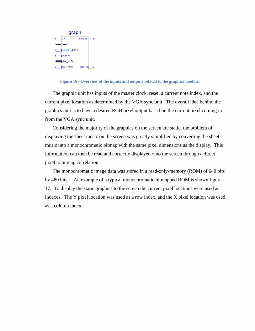
Figure 16 - Overview of the inputs and outputs related to the graphics module.
The graphic unit has inputs of the master clock, reset, a current note index, and the
current pixel location as determined by the VGA sync unit. The overall idea behind the
graphics unit is to have a desired RGB pixel output based on the current pixel coming in
from the VGA sync unit.
Considering the majority of the graphics on the screen are static, the problem of
displaying the sheet music on the screen was greatly simplified by converting the sheet
music into a monochromatic bitmap with the same pixel dimensions as the display. This
information can then be read and correctly displayed onto the screen through a direct
pixel to bitmap correlation.
The monochromatic image data was stored in a read-only-memory (ROM) of 640 bits
by 480 bits. An example of a typical monochromatic bitmapped ROM is shown figure
17. To display the static graphics to the screen the current pixel locations were used as
indexes. The Y pixel location was used as a row index, and the X pixel location was used
as a column index.

Figure 17 - Displaying a typical condensed ROM unit and methods for retrieving an individual
bit to output to the VGA display.
For example, if VGA sync specifies that the current Y pixel location was 0x01 then
the resulting ROM_row would be the following:
ROM_row <=ROM(1) = "0111...1110"
Furthermore, if the VGA sync also specified that the current X pixel was 0x02, then
the resulting ROM_bit would be '1'. These individual bits are the determining factor as to
whether the current pixel on the screen should be on or off.
12.2.6 Text Output
The text unit is the module that coordinates all ASCII text characters displayed on the
screen at any given time. Each ASCII character is treated as a tile read from a character
set, or font, specified by a 7-bit ASCII code. The text unit's main purpose is to output the
current number of notes correctly played, and the number of notes or chords incorrectly
played to the VGA monitor. An overview of the inputs and outputs of this unit are
displayed in figure 18.

Figure 18 - Overview of inputs and outputs of the text module.
The text module takes in inputs of the current pixel x and pixel y locations as
determined by the VGA synchronization unit. This allows the text unit to know the
location of the current pixel being updated on the VGA monitor. Based on the current
pixel the correct bits corresponding to the correct letter can then be determined.
The module also takes in inputs for the hit and miss counters. The digits of the
counters are passed individually as a single digit. In ASCII, any number can be
represented by 0x3N, where N is the desired number. Therefore, the digit can then be
referenced as an ASCII character in the character ROM as constant hexadecimal 3
concatenated with the 4-bit digit coming into the text unit.
12.2.7 Final VHDL Schematic
The final VHDL schematic displaying all of the individual components and modules
connected together is shown in figure 19. All signals outside of the main rectangle are
physical inputs and outputs that the hardware is controlling. These are the physical
connections such as push buttons, a rotary knob, VGA cable, etc. On the other hand,
everything inside of the box is the result within the FPGA produced by the hardware
description language. These are the inner workings of the FPGA, which the user does not
physically have access.

Figure 19 ‐ Final VHDL schematic containing all necessary modules.

12.3 Engineering Analysis and Calculations
12.3.1 LEDs
To ensure that the LEDs would perform adequately calculations regarding the current
flow were necessary. This not only guaranteed proper luminosity but it also eliminated
the possibility of destroying the unit itself. To accomplish this the implementation of a
resistor was needed which was placed in series to the LED in between the decoder output
and the LED, to determine the value of the resistor Ohms Law was used (V=IR). Given
The Voltage source (3v) as well as the current limitations (20mA) of the LED solving for
R was a simple Algebraic manipulation that resulted in R = 150 ohms. Polarity was very
important to ensure proper behavior, since incorrect wiring of the LED’s polarity would
result in no current flow and no light, also the LED would be destroyed. To prevent this
manufactures use indicators. The first indicator; on the red LED the longer wire shows
the anode (+) side and the shorter the Cathode (-). The green LED’s indicator was
different on one side the LED there was a Flat spot, indicating the Cathode implying the
other side is the anode. For the fabrication of the Strip the LED’s were set in parallel, and
because of this layout every LED required to have its own resistor, not only would more
than one LED that shared a common resistor would loss luminosity to a point that no
light would be emitted but it wouldn’t be possible to turn only one LED without turning
the other on. The cathode side of the LEDs were connected on a common ground this
flagged the possibility of EMI and as a precaution measurement to prevent any margin of
error some research in the matter was made, after further investigation it was found that
this phenomena would have minimal effect in the strip with a possible slight affect in
luminosity which is negligible.
12.3.2 VHDL Programming Code
A minor calculation was required to generate a tick counter from the 50MHz clock on
the FPGA board. The tick counter was used to count from 0 to 15 in between each
incoming bit on the UART module. Since the baud rate for a MIDI signal is 31,250 bits
per second, the sampling rate must then be

The mod-counter value needed was then calculated by
13.0 Major Problems
13.1 FPGA Glitches
Several problems occurred while debugging the code. VHDL is a bit different from
the most familiar C and C++ because VHDL is not sequential. The processes all occur
simultaneously, so debugging code would sometimes take hours. One of the glitches
occurred in the filter unit. When the keys were pressed at a slow tempo, the output key
would be flawless, however as the tempo increased, the error increased. The filter was
not filtering the “velocity” and “note off” bytes. After hours of debugging, another state
diagram was formulated and the code was re-written. The problem was the nesting of the
conditional “if statements” and “case statements”. After meticulously re-writing the code,
the filter unit worked flawlessly without any glitches.
13.2 Latched Mux Fix
A problem arose once testing of the decoder circuit began. The design requires
another LED to illuminate when prompted, turning off the previous illuminated LED.
When tested, the decoder circuit kept the previous LED illuminated if the next LED to be
illuminated was connected to another multiplexer, causing 2 LEDs to light up
simultaneously. After researching the specifications of the multiplexers, it was
determined that latching of the multiplexers was causing this problem. When the strobe
(LE) input was high and the inhibit input was low it would enable the multiplexer to
select an output, but when the inhibit input was low and the strobe (LE) input was low the
selection would remain selected until the strobe (LE) input was high again. It was
discovered that regardless of the strobe (LE) input, that if the inhibit were high all outputs
would be set to zero, Figure # displays the truth table for this component. To fix this
problem, we needed the inhibit inputs of the multiplexers to be high when they weren’t
selected. This problem was solved by adding a NOR gate between the levels of
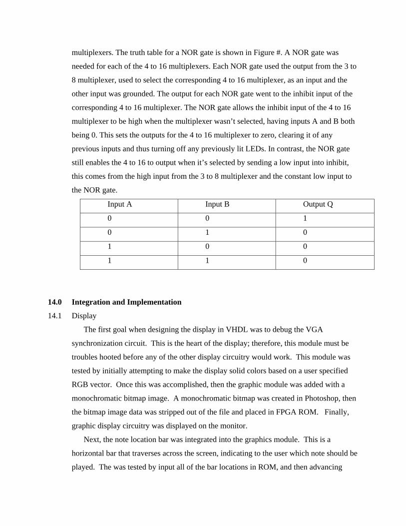
multiplexers. The truth table for a NOR gate is shown in Figure #. A NOR gate was
needed for each of the 4 to 16 multiplexers. Each NOR gate used the output from the 3 to
8 multiplexer, used to select the corresponding 4 to 16 multiplexer, as an input and the
other input was grounded. The output for each NOR gate went to the inhibit input of the
corresponding 4 to 16 multiplexer. The NOR gate allows the inhibit input of the 4 to 16
multiplexer to be high when the multiplexer wasn’t selected, having inputs A and B both
being 0. This sets the outputs for the 4 to 16 multiplexer to zero, clearing it of any
previous inputs and thus turning off any previously lit LEDs. In contrast, the NOR gate
still enables the 4 to 16 to output when it’s selected by sending a low input into inhibit,
this comes from the high input from the 3 to 8 multiplexer and the constant low input to
the NOR gate.
Input A Input B Output Q
0 0 1
0 1 0
1 0 0
1 1 0
14.0 Integration and Implementation
14.1 Display
The first goal when designing the display in VHDL was to debug the VGA
synchronization circuit. This is the heart of the display; therefore, this module must be
troubles hooted before any of the other display circuitry would work. This module was
tested by initially attempting to make the display solid colors based on a user specified
RGB vector. Once this was accomplished, then the graphic module was added with a
monochromatic bitmap image. A monochromatic bitmap was created in Photoshop, then
the bitmap image data was stripped out of the file and placed in FPGA ROM. Finally,
graphic display circuitry was displayed on the monitor.
Next, the note location bar was integrated into the graphics module. This is a
horizontal bar that traverses across the screen, indicating to the user which note should be
played. The was tested by input all of the bar locations in ROM, and then advancing

through the notes using a pushbutton. Initially a pushbutton was used to rule out any
errors from any other modules. Once the module was correctly advancing the bar across
the screen, it was then ready to be integrated with the note timing unit.
14.2 UART
The output of the UART VHDL circuitry was initially tested using the UART tool
provided through the PICkit 2. Once a successful signal was output, a filter was set up to
only display the required note byte and disregarded the other information. This filtered
information was tested by visually representing the desired byte on the discrete LEDs of
the Basys board.
14.3 Timing and Note Detection
The note timing unit was first tested to be able to correctly select the correct note
which should be played at that moment. This was accomplished by setting up an timer
which advanced the notes. This timer was tested by outputting this value to a discrete
LED on the board, thereby allowing a visual representation of the note timer. After this
timer was function properly, the timer was integrated with the graphic display. The note
timer was used to advance an index which was passed to the graphic unit. This signal
replaced the earlier program of advancing the traversing line by pushbutton.
After it was proven on the VGA display that as the note timer was overflowing, the
notes were changing across the screen, it was them time to incorporate the note detection
scheme. Initially, only one value was being detected for the UART MIDI output. This
was done to simplify the problem. In order to test the note detection scheme, the PICkit
UART tool was used as a simulated keyboard input. As the notes were advancing across
the screen, the UART tool was set up to send a constant note, which cleared the
performance flags, thereby indicating that a note was correctly pressed. When a flag was
cleared, this was output to the LEDs on the Spartan Board. This allowed a visual
representation of then digital signals.
Finally, after it was tested that a single note could be correctly detected and counted,
all of the VHDL modules were integrated together. The note detection unit was set up to
detect chords, rather than single notes. This was just a trivial extension of detecting a

single note. Finally, the counters were updated based on whether or not the notes were
hit or missed. This was visually represented on the VGA display.
14.4 LED Strip
The soldering of all of the individual LEDs on the LED strip is a tedious process. All
LEDs were checked for correct voltage polarity. Due to the numerous number of
connections that must be made, all solder joints were meticulously checked for integrity
and continuity. Finally, after verification of the correct polarity for each individual LED,
each LED was individually tested to verify correct operation.
14.5 Decoder Circuitry
The decoder circuitry was initially wired on a breadboard. Then, to test the correct
operation of the circuit, each of the inputs was manually tied to either a digital high or
low. Based on the combination of digital highs and lows set up as inputs, the output was
tested to verify proper functionality. For any given input combination, only one output
should be high and the others should remain low. Each output was tested under different
combinations to verify that this held true.
15.0 Comments and Conclusion
This project provided the team with excellent learning experience. It allowed the team
to gain insight into project planning from the design phase all the way to implementation
and presentation. It also allowed each member to contribute their diverse knowledge and
skills and collaborate that with other members to complete the project.
16.0 Team Members
16.1 Emiliano Morales
Emiliano Morales’ top priority for the construction of the PT2009X was deciphering
the signal from the MIDI-out port so that it could be used by the system to determine
whether a note has been hit or not. This gave him the responsibility of understanding the
concept behind UART and applying this to the project. His achievements include being

able to successfully retrieve signals from the keyboard through the use a the MIDI to
FPGA interface circuit and being able to decipher the signal and retrieve the byte
corresponding to the notes without any false readings. Some of his leadership roles
include the responsibility of overseeing the progress of each member. The members of
the team reported the milestones completed, this allowed for a more efficient task
distributions. He was also the record keeper of the team, by logging all progress and
problems in a managerial notebook. This notebook also kept track of the expenses done
in the project.
16.2 Rebecca Conner
Rebecca worked primarily with the decoder circuit, from design to implementation.
She was responsible for ensuring the proper functionality of the component, so that it
could properly interact with the other components of the design. She built the decoder
circuit and developed a solution to fix the latching problem that arose with the
multiplexers. She rigorously tested the circuit at each stage of development ensuring the
end result to be completely functional and capable of doing what the design intended it
for. Rebecca also assisted in researching and purchasing the strip material, as well as
testing components of the LED strip. She also created and maintained the team’s website
and put together Visio drawings and animations needed for presentations and reports. In
addition, to help ensure the project was done in a timely manner, she assisted the team in
keeping track with deadlines.
16.3 Christopher Montanez
Christopher's primary role in the project consisted of research, design, VHDL
programming, and testing for the VGA display, Timing Units, and Note Detection based
on the output provided by the UART module. His achievements were being able to
successfully design and implement a VHDL design that had the capability to output text
and graphics to a VGA monitor. Also, using VHDL he was able to create modules that
allowed for a variable song tempo, proper detection of multiple notes within a chord, and
updating of counters which were then output as text to the VGA monitor. He also wrote
code which allowed for a scanning display of the LEDs for the LED strip. This allowed
for multiple LEDs appear to be on at the same time. He participated in updating of the
weekly presentations and edited, and wrote sections of the final report.
16.4 Mario Espinoza
Mario’s role in this project consisted in the following areas research, design,
presentation, and construction. In the initial stages he was given the task to research the
alternatives to drive seventy-six LED’s from a seven pin output. He was also in charge of
determining the parts and components for the selected design. The finalized design in the
multiplexing section was performed by Rebecca Conner, his contribution on that matter
consisted in attempting the first circuit design. This consisted of constructing the circuit
and performing tests to determine if its functionality would perform as needed, minor
complications arose and it was given to Rebecca. Then he was assigned the role of
constructing the LED strip. Here, Mario’s soldering skills were utilized to solder 152
points in the LED circuit. The LED strip consisted on selecting the proper dimensions,
material, and performing diverse tasks, like cutting and drilling of seventy-six LED holes.
He also installed LED mounting holders with their corresponding retainers. The strip
required Mario to research design techniques regarding resistor selection, LED
limitations, wire tolerations, and EMI created by the ribbon wire. Mario also contributed
in different parts of the report, and presentations with respect to the status of the project.

17.0 References
Chu, Pong P. FPGA Programming by VHDL Examples. Hoboken: Wiley‐Interscience, 2008.
Digilenent, Inc. VGA Reference Component. 2008 March 28.
Digilent, Inc. Digilent Basys Reference Manual. 18 August 2007.
Digilent, Inc>. Spartan‐3E Starter Kit User's Guide. 9 March 2006.