Takahide Kadoyama Device&Circuit Development Department Micro Systems Network Company Sony...
32
Takahide Kadoyama Device&Circuit Development Department Micro Systems Network Company Sony Corporation A Complete Single-Chip GPS Receiver
-
Upload
annice-porter -
Category
Documents
-
view
217 -
download
0
Transcript of Takahide Kadoyama Device&Circuit Development Department Micro Systems Network Company Sony...
Takahide Kadoyama
Device&Circuit Development DepartmentMicro Systems Network Company
Sony Corporation
A Complete Single-Chip GPS Receiver
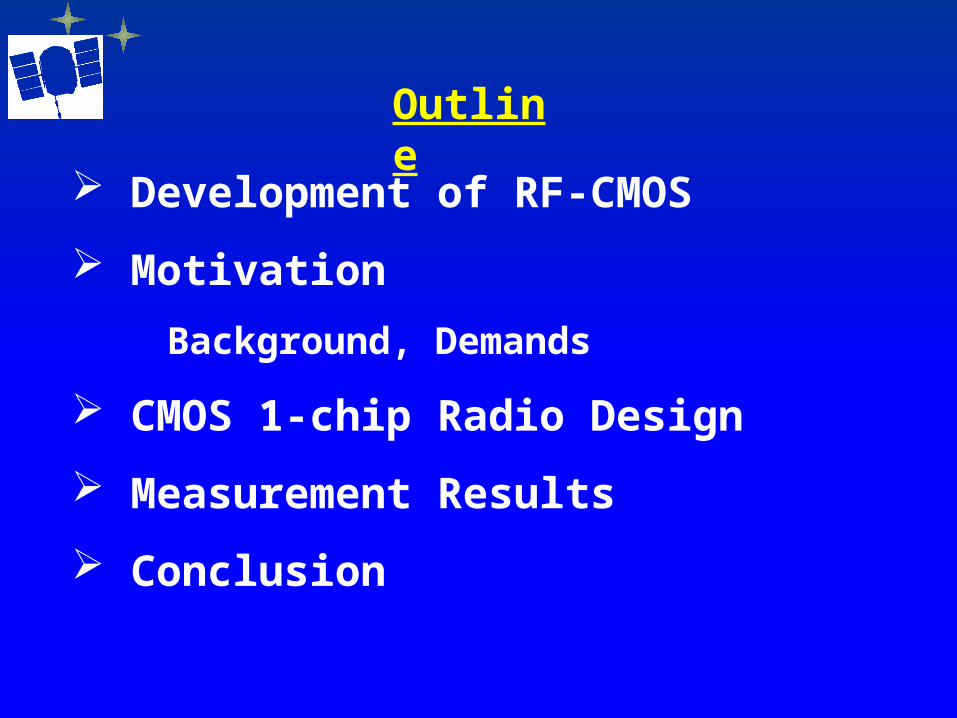
Development of RF-CMOS
Motivation
Background, Demands
CMOS 1-chip Radio Design
Measurement Results
Conclusion
Outline

2000 Bluetooth Radio+BB SoC 0.35 um CMOS CSR Product
2001 IEEE802.11a Radio 0.25 um CMOS Athelos Product
2002 GPS Radio 0.35 um CMOS Valence ISSCC
2003 GPS Radio + BB SoC 0.18 um CMOS Sony VLSI
Development of RF-CMOS Products

Bluetooth on SoC (-85 dBm) :AccomplishedGPS on SoC (-150 dBm) : This Work
Bluetooth vs. GPS Input Sensitivity
-85 dBm
-150 dBm
Thermal Noise
Freq.
Bluetooth
GPS
-110 dBm
Input Power
A digital wireless technology that uses a "spread spectrum" technique to scatter a radio signal across a wide range of frequencies.
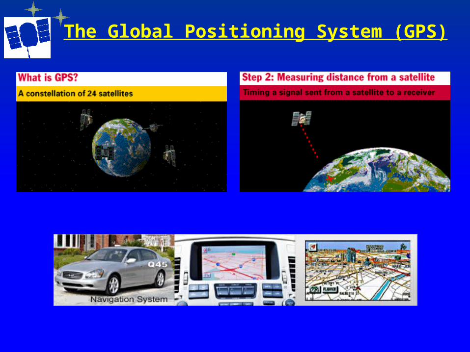
The Global Positioning System (GPS)
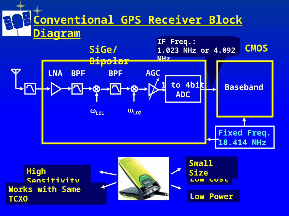
1 to 4bitADC
Baseband
LNA AGCBPF
Conventional GPS Receiver Block Diagram
SiGe/Bipolar CMOS
High Sensitivity
Low Power
Low Cost
Fixed Freq.18.414 MHz
Small Size
Works with Same TCXO
BPF
LO1 LO2
IF Freq.: 1.023 MHz or 4.092 MHz
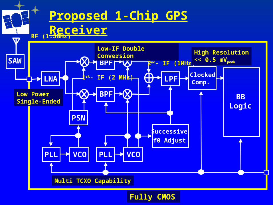
LNA
PSN
VCO
BPF
BPF
VCOPLL PLL
LPFClockedComp.
Successive
f0 Adjust
SAW
Proposed 1-Chip GPS Receiver
RF (1.5GHz)
1st- IF (2 MHz)
2nd- IF (1MHz)
BBLogic
Fully CMOS
High Resolution<< 0.5 mVpeak
Low PowerSingle-Ended
Multi TCXO Capability
Low-IF Double Conversion

2.3 mm
CMOS 1-Chip Receiver
6.3 mm
6.3
mm
0.18 um CMOS + MIM cap. / Deep N-Well 500K Gates / 176 Pads Mask ROM, SRAM, Dual Port SRAMFrequency : BB-74 MHz, RF-1.5 GHz
ROM
RAM
2.0
mm
VCO
LNA/MixIF Stage
Radio

Low Power Consumption
24 mW in Radio
(Valence:27 mW)
57 mW for Fully Functional Chip
(Motorola :200 mW)
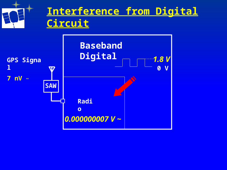
Radio
Baseband Digital
Interference from Digital Circuit
SAW
GPS Signal
7 nV ~
1.8 V0 V
0.000000007 V ~
Radio
Baseband Digital
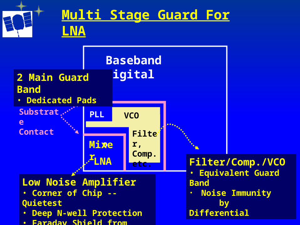
Multi Stage Guard For LNA
Mixer
LNA
Low Noise Amplifier• Corner of Chip -- Quietest• Deep N-well Protection• Faraday Shield from Substrate
PLL
Filter,Comp.etc.
Filter/Comp./VCO• Equivalent Guard Band• Noise Immunity by Differential
VCO
2 Main Guard Band• Dedicated Pads
SubstrateContact

Low Noise Amplifier
VCO IF Stage
Simulated Substrate Noise Propagation
Noise Level
Large
Small
Baseband Digital
NoiseSource(1.5 GHz)
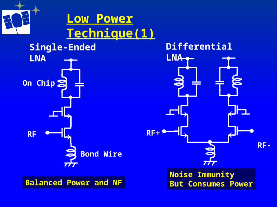
Low Power Technique(1)
Bond Wire
On Chip
Balanced Power and NF
Single-Ended LNA
RF+
RF-
Noise ImmunityBut Consumes Power
Differential LNA
RF
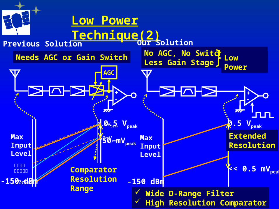
Previous Solution
Low Power Technique(2)
0.5Vpeak
許容最大入力レベル
-150dBm
50mVpeak
0.5 Vpeak
50 mVpeak
-150 dBm
Max InputLevel
Needs AGC or Gain Switch
Comparator Resolution Range
Our Solution
+
0.5 Vpeak
-150 dBm
Max InputLevel
<< 0.5 mVpeak
-
ExtendedResolution
Wide D-Range Filter High Resolution Comparator
No AGC, No SwitchLess Gain Stage
Low Power
+-
AGC
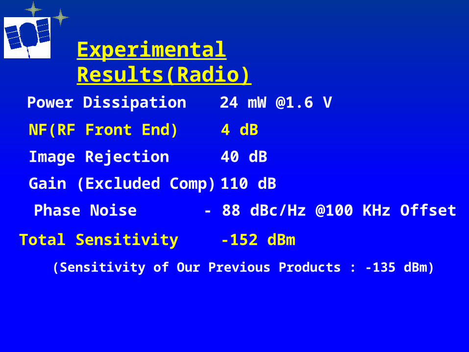
Experimental Results(Radio)
Total Sensitivity -152 dBm
Power Dissipation 24 mW @1.6 V
NF(RF Front End) 4 dB
Image Rejection 40 dB
Gain (Excluded Comp) 110 dB
Phase Noise - 88 dBc/Hz @100 KHz Offset
(Sensitivity of Our Previous Products : -135 dBm)

Video ClipAcquisited Satellites
8 satellites are tracked
Weak Strong
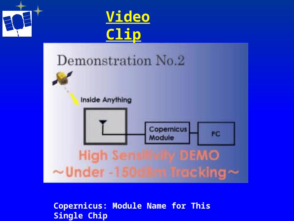
Video Clip
Copernicus: Module Name for This Single Chip

Conclusions
Complete Single-Chip GPS Receiver
Low Power Consumption in Radio : 24 [email protected] V
Substrate Noise Overcome by Multistage Guard
Total Sensitivity of -152 dBm

Appendix
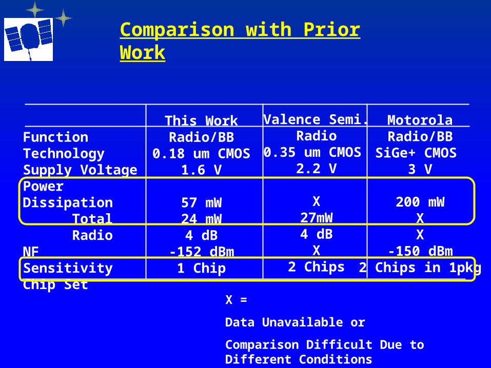
Comparison with Prior Work
MotorolaRadio/BB
SiGe+ CMOS 3 V
200 mWXX
-150 dBm2 Chips in 1pkg
Valence Semi.Radio
0.35 um CMOS 2.2 V
X27mW4 dB
X2 Chips
This WorkRadio/BB
0.18 um CMOS1.6 V
57 mW24 mW4 dB
-152 dBm1 Chip
FunctionTechnologySupply VoltagePower Dissipation
TotalRadio
NFSensitivityChip Set
X =
Data Unavailable or
Comparison Difficult Due to Different Conditions
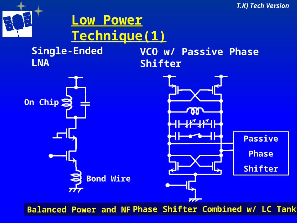
Low Power Technique(1)
Bond Wire
On Chip
Passive
Phase
Shifter
Balanced Power and NF Phase Shifter Combined w/ LC Tank
Single-Ended LNA VCO w/ Passive Phase Shifter
T.K) Tech Version
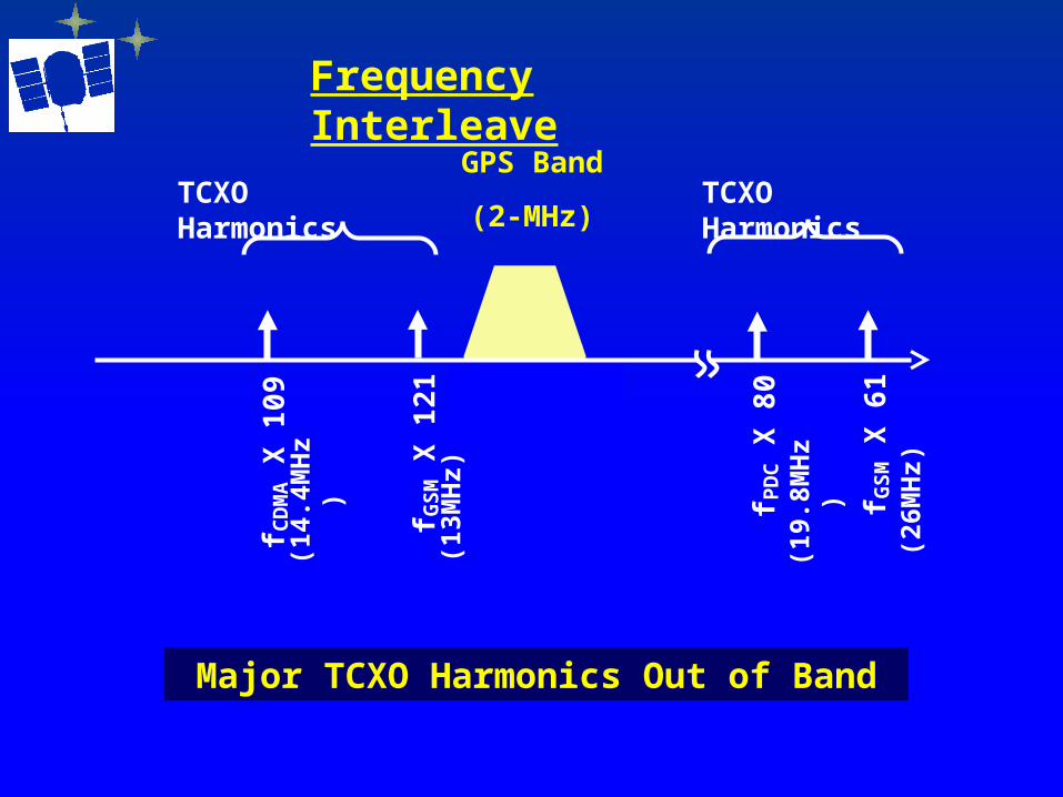
Frequency Interleave
GPS Band
(2-MHz)
f GS
M X
12
1
f CD
MA X
10
9
f GS
M X
61
(26M
Hz)
(13M
Hz)
f PD
C X
80
(14.
4MH
z)
(19.
8MH
z)
TCXO Harmonics TCXO Harmonics
Major TCXO Harmonics Out of Band
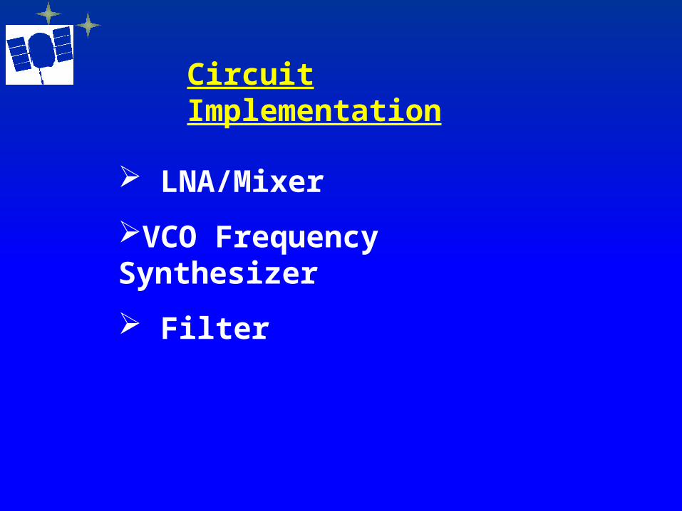
LNA/Mixer
VCO Frequency Synthesizer
Filter
Circuit Implementation
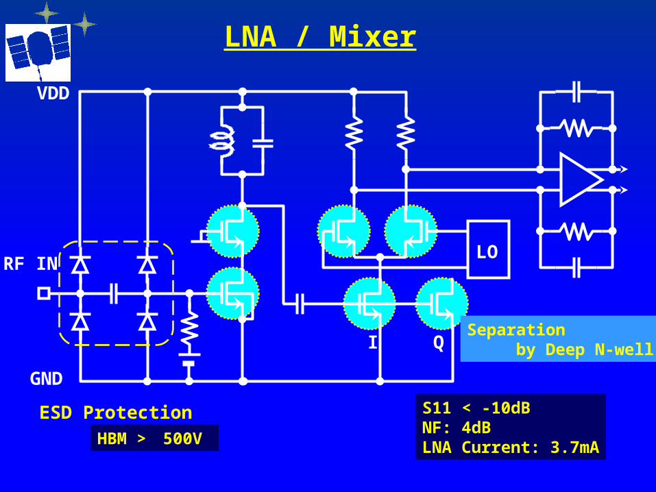
LNA / Mixer
ESD Protection
I Q
LO
S11 < -10dBNF: 4dBLNA Current: 3.7mAHBM > 500V
Separation by Deep N-well
VDD
GND
RF IN
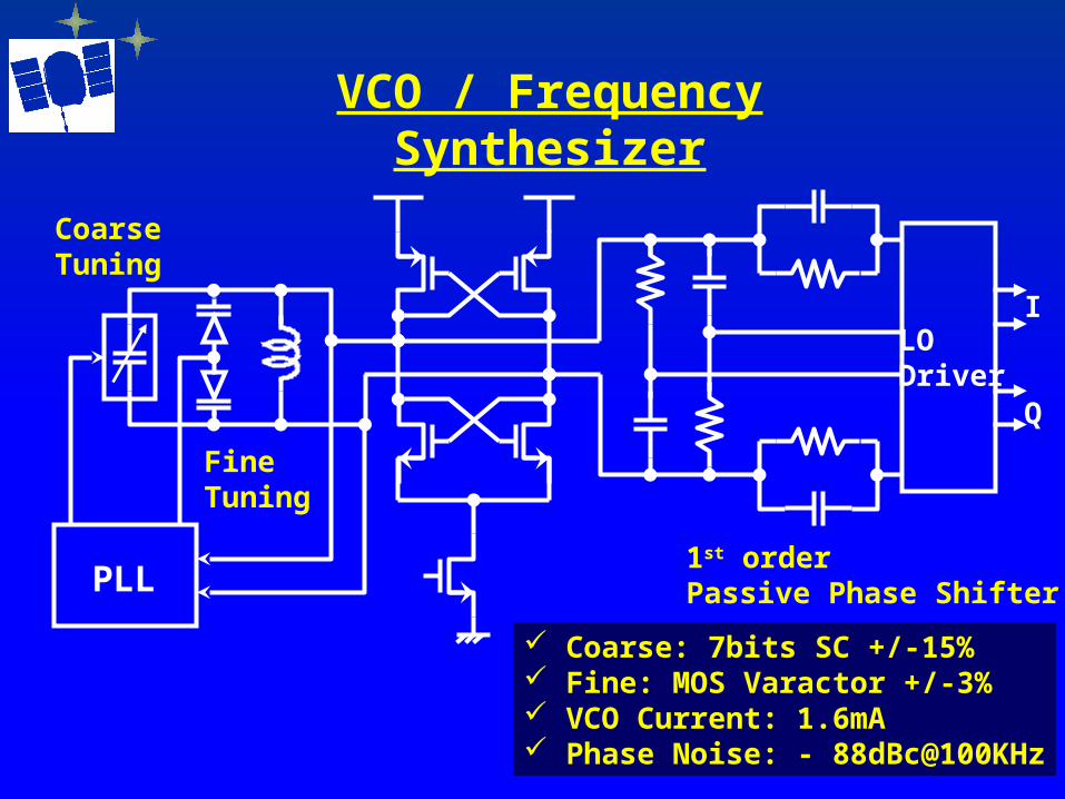
VCO / Frequency Synthesizer
FineTuning
CoarseTuning
1st orderPassive Phase ShifterPLL
LODriver
I
Q
Coarse: 7bits SC +/-15% Fine: MOS Varactor +/-3% VCO Current: 1.6mA Phase Noise: - 88dBc@100KHz
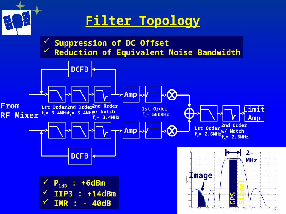
Filter Topology
Suppression of DC Offset Reduction of Equivalent Noise Bandwidth
From RF Mixer
Amp
DCFB
Amp
DCFB
LimitAmp
1st Orderfc= 3.4MHz
2nd Orderfc= 3.4MHz
2nd Orderw/ Notchfc= 3.4MHz
1st Orderfc= 500KHz
1st Orderfc= 2.6MHz
2nd Orderw/ Notchfc= 2.6MHz
P1dB : +6dBm IIP3 : +14dBm IMR : - 40dB G
PS
Sig
nal
Image
2-MHz

IF VCO12MHz
SuccessiveApproximation
Logic
PhaseComparator
Sine WaveGenerator
Clock Generator
4bit Resistor Bank
Replica Filter
Filter Tuning Topology
+-+
-
IF Filter
8R
4R
12R
R0
2R
R
3R
Reference(3MHz)
4
25
27
29
31
33
35
37
39
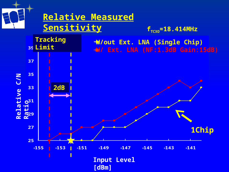
-155 -153 -151 -149 -147 -145 -143 -141
Relative Measured SensitivityR
ela
tiv
e C
/N R
ati
o
fTCXO=18.414MHz
Input Level [dBm]
W/out Ext. LNA (Single Chip) W/ Ext. LNA (NF:1.3dB Gain:15dB)
Tracking Limit
2dB
1Chip

+
-+
-
if1amp
+-+
-
filter_11 filter_12 filter_13
if mixer
OPamp+-+
-+-+
- +-+
-+-+
-OPamp OPamp OPamp OPamp
OPamp
+-+
-OPamp
Mixer out
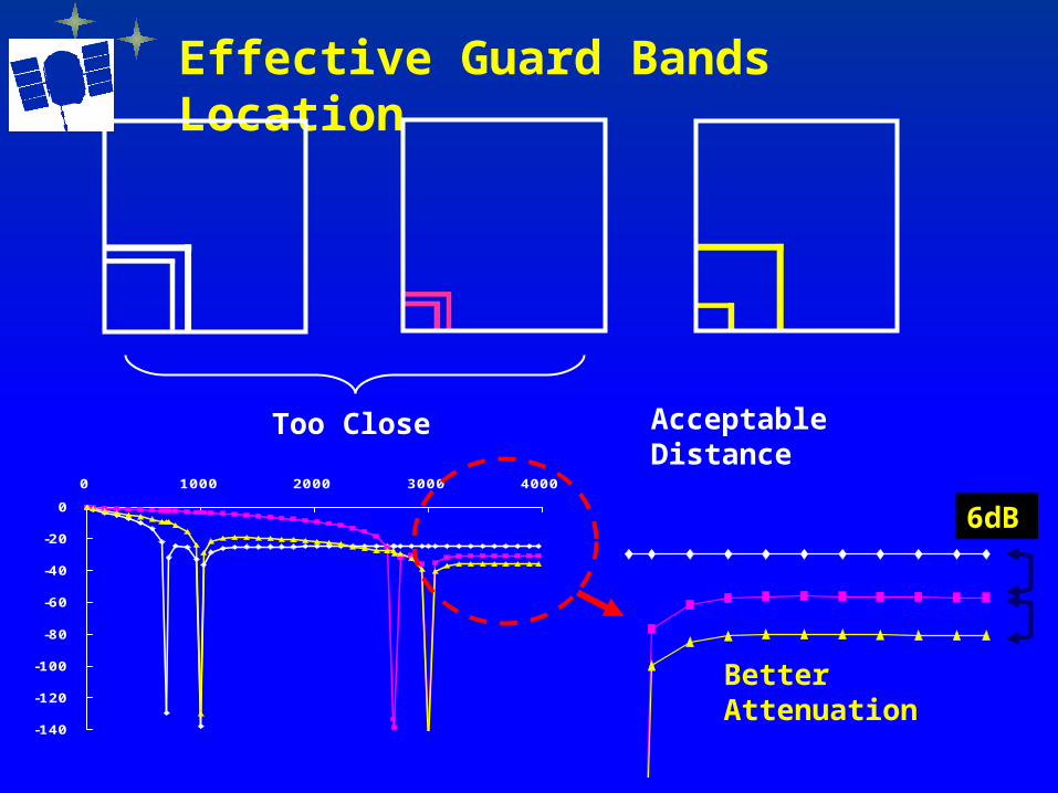
Effective Guard Bands Location
Too Close Acceptable Distance
-140
-120
-100
-80
-60
-40
-20
0
0 1000 2000 3000 4000
Better Attenuation
6dB
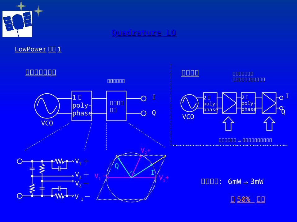
Quadrature LOQuadrature LO
LowPower技術 1
消費電力: 6mW 3mW⇒
約 50% 削減
V1+
V2+V2-
V 1-
ゲイン段必要⇒消費電力が大きくなる
高次フィルタで直交周波数範囲を大きく
2次poly-phase
2次poly-phase
VCO
I
Q
従来技術新規回路を開発
1次poly-phase
I
Q
VCO
ベクトル合成
原理的に直交
V2+
V1+I
Q
V1-
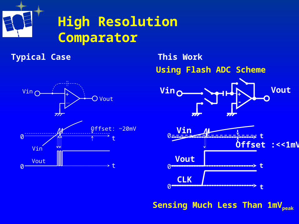
Using Flash ADC Scheme
+Vin Vout
Offset: ~20mV
0
0 t
t
Vin
Vout
Offset :<<1mV0
t
Vin
Vout
CLK
0
0
-+Vin
Vout
Sensing Much Less Than 1mVpeak
High Resolution Comparator
Typical Case This Work
-
t
t


![MULTI CHANNEL AV RECEIVER STR-DH770 - Sony CHANNEL AV RECEIVER STR-DH770 Parts and Controls Receiver ... [18] Connecting 5.1-channel speaker system with front …](https://static.fdocuments.in/doc/165x107/5ab5b3567f8b9a6e1c8d1f5c/multi-channel-av-receiver-str-dh770-sony-channel-av-receiver-str-dh770-parts-and.jpg)