Tackling Electrical Variability in Advanced CMOS Technologies
46
1 Tackling Electrical Variability in Advanced CMOS Technologies Xi-Wei Lin [email protected] IMPACT Webinar, May 15, 2009, UC Berkeley
Transcript of Tackling Electrical Variability in Advanced CMOS Technologies

1
Tackling Electrical Variability
in Advanced CMOS Technologies
Xi-Wei Lin
IMPACT Webinar, May 15, 2009, UC Berkeley

2
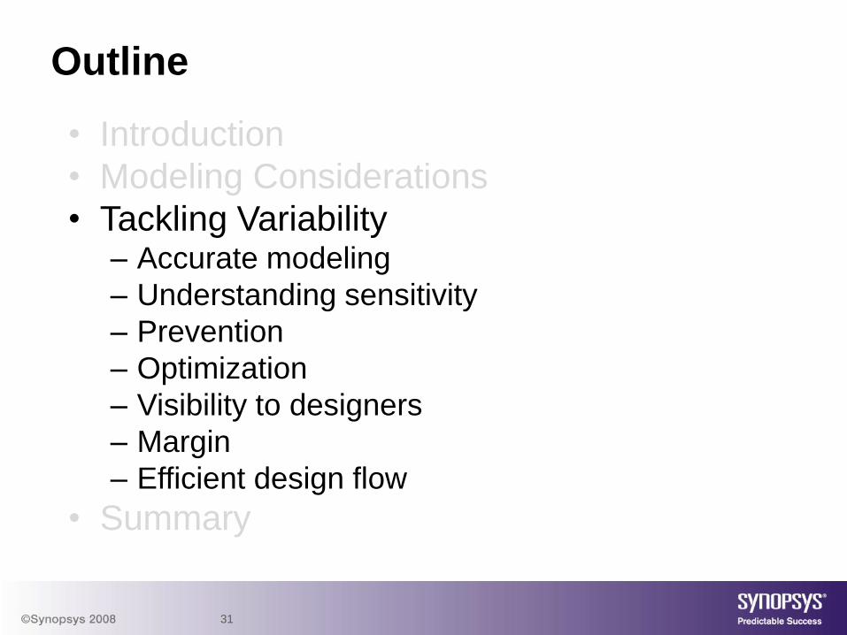
• Introduction
• Modeling Considerations
• Tackling Variability
• Summary
Outline
3
• Introduction
– Proximity effects : litho, stress, Vth
• Modeling Considerations
• Tackling Variability
• Summary
Outline
4
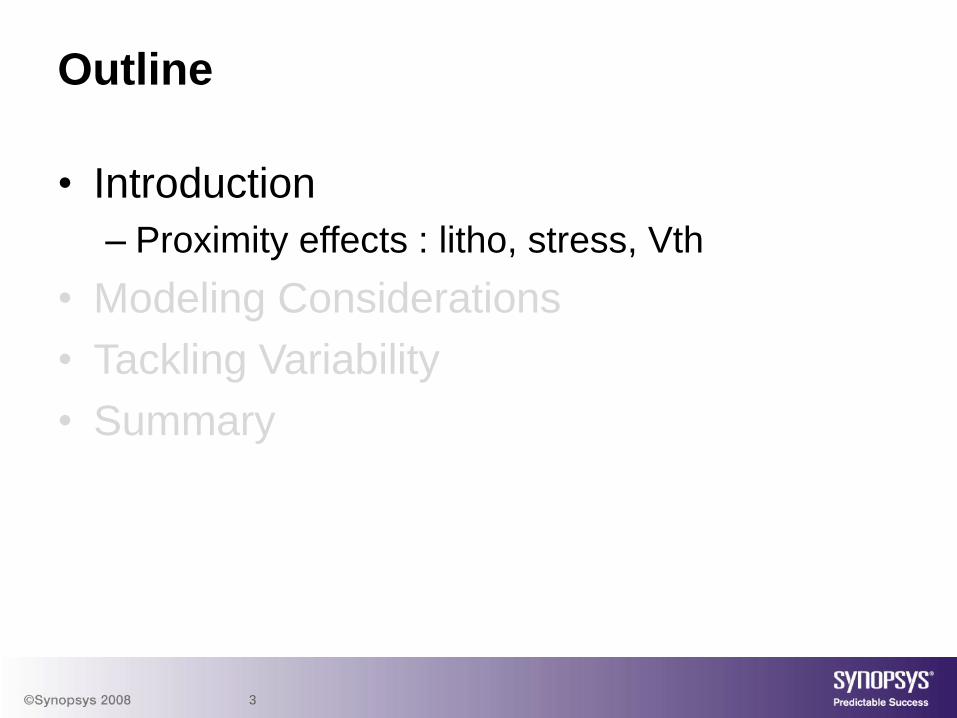
Process and Layout Interactions
• Systematic, layout dependent variations result from process and layout interactions.
• The enabling manufacturing processes are inherently coupled with design.
Design
Layout
Process
Module
Enabling
Design
En
ab
lin
g T
ech
no
log
y
Physical
Design
Strain
Engineering
Others
(deep well, …)
Dummy fill(Diff, Metal, …)
CMPR & C
Variations
Sub-l lithoMask Synthesis
(OPC, PSM, …)
CD / Shape
Variations
Mobility
Variations
Vth, …
Variations
Primary
Effects
5
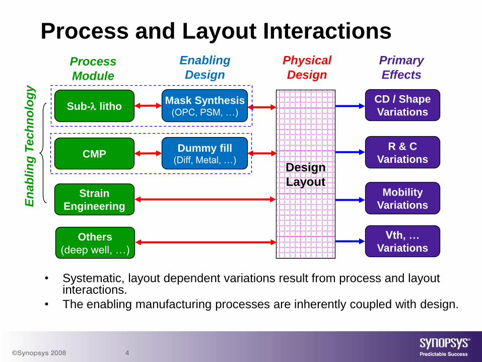
Sources of Layout Proximity Variations
Cap layer
SiGe S/D
Gate Spacer
STI
X
Y
Z
Lithographic Proximity : Poly and Diffusion
Mechanical stress due to STI, SiGe, ESL, SMT, …
Well Proximity (WPE), transient -enhanced diffusion (TED), …

6
Corner Rounding Gets Worse
• Different W’s require jogs in diffusion mask
The jogs have a fixed curvature radius of
~60nm that can not be improved by OPC.
Meanwhile, the poly pitch shrinks by 0.7x with
each technology node
The channel shapes become distorted
acti
ve
po
ly
po
ly
po
ly
STI
• How does it affect transistor performance?
Poly gate shape – distorted channel length
Active layer shape – varied channel width
Max variation at 45nm :
L ~ 5%
W ~ 10%
Overlay error (misalignment) aggravates the
channel distortion.

7
Strain Engineering
• Stress sources:– Stress liner (ESL) : single or dual
– Embedded SiGe (S/D)
– Stress memorization technique
– Strain-Si/SiGe
– Trench contacts
– STI
Horstmann et al. 2005
NMOS
PMOS
NiSi
spacer
NiSi
Tensile stress liner
SiGeSiGe
NiSi
Compressive stress liner
An enabling technology since 90nm
8
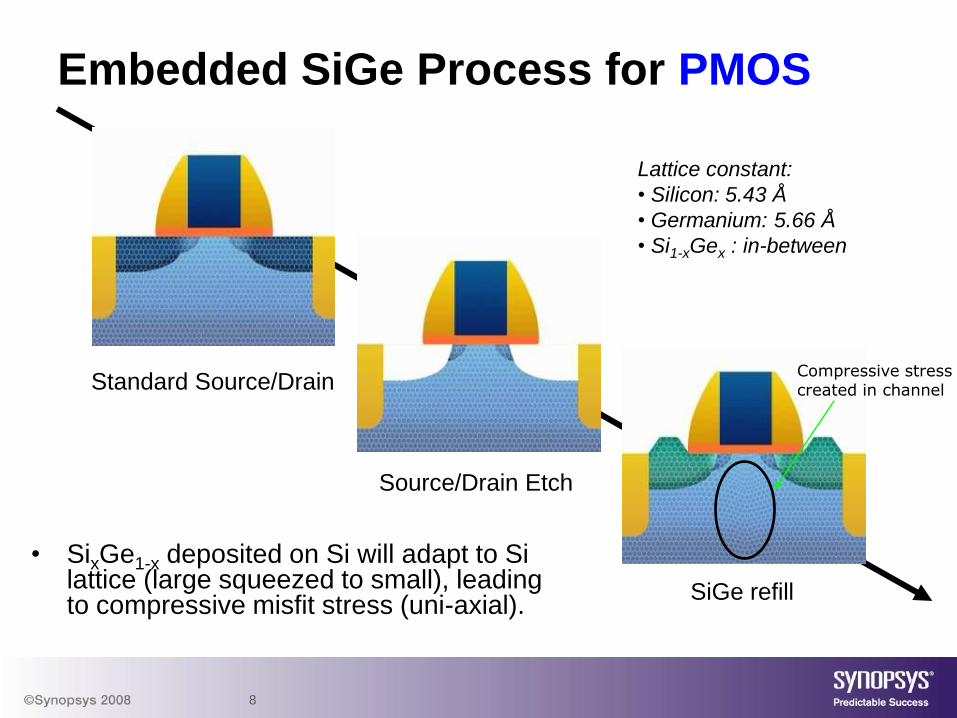
Embedded SiGe Process for PMOS
• SixGe1-x deposited on Si will adapt to Si lattice (large squeezed to small), leading to compressive misfit stress (uni-axial).
Standard Source/Drain
Source/Drain Etch
Compressive stress created in channel
SiGe refill
Lattice constant:
• Silicon: 5.43 Å
• Germanium: 5.66 Å
• Si1-xGex : in-between
9
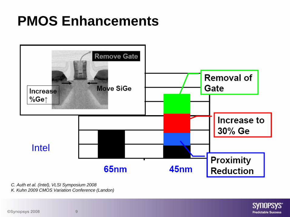
PMOS Enhancements
C. Auth et al. (Intel), VLSI Symposium 2008
K. Kuhn 2009 CMOS Variation Conference (Landon)
Intel
10
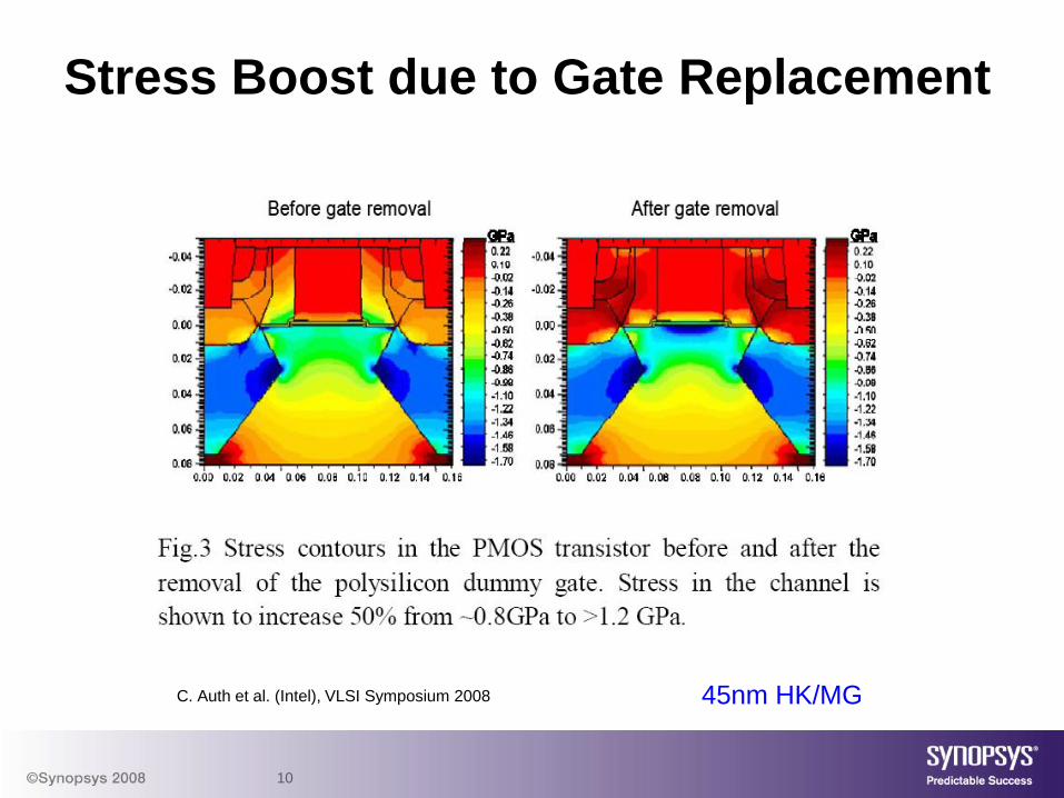
C. Auth et al. (Intel), VLSI Symposium 2008
Stress Boost due to Gate Replacement
45nm HK/MG

11
Contact and Gate Induced Stress
• NMOS Enhancement (45nm HK/MG)
C. Auth et al. (Intel), VLSI Symposium 2008
K. Kuhn 2009 CMOS Variation Conference (Landon)
12
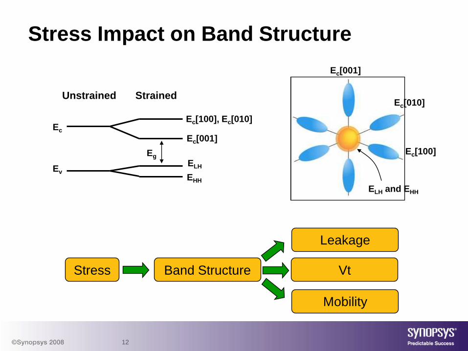
Stress Impact on Band Structure
Ec[100]
Ec[001]
Ec[010]
ELH and EHH
Ec[001]
Ec[100], Ec[010]
ELH
EHH
Ec
Ev
Unstrained Strained
Stress Band Structure
Mobility
Vt
Leakage
Eg

13
Complexity of Stress Effects on Mobility
Electron and hole mobility change per 1 GPa
stress, based on piezoresistance effect
Stress component
Tensile Compressive
nMOS pMOS nMOS pMOS
1 GPa along channel (X)
Longitudinal+30% -70% -30% +70%
1 GPa across channel
(Z), Transverse+20% +70% -20% -70%
1 GPa vertical (Y)
Out of plane-50% +1% +50% -1%
Piezoresistance coefficients are valid under small and moderate stress, where the piezoresistance varies linearly with stress.
1111
Y
XZ
• Direction
• Sense
• Type
Wafer orientation: (100)/<110>
14
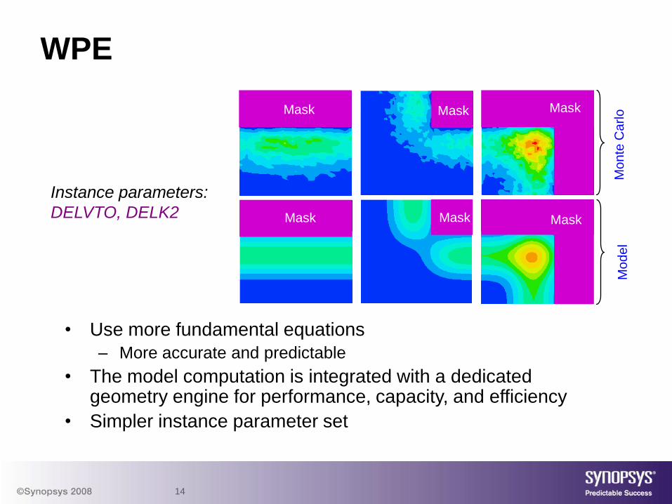
WPE
• Use more fundamental equations
– More accurate and predictable
• The model computation is integrated with a dedicated geometry engine for performance, capacity, and efficiency
• Simpler instance parameter set
Mask Mask Mask
Mask Mask Mask
Mo
nte
Ca
rlo
Mo
de
l
Instance parameters:
DELVTO, DELK2

15
Threshold Variation Due to STI Proximity
S SD D
Vtlin=298mV
Idlin=152uA
Vtlin=350mV (+52mV)
Idlin=130uA (-15%)
a b
ST
I
ST
I
S SD D
Vtlin=298mV
Idlin=152uA
Vtlin=350mV (+52mV)
Idlin=130uA (-15%)
a b
ST
I
ST
I
Nested nMOSFET Isolated nMOSFET
Less TED with B asymmetry due to the
different proximity of STI behind S & D
Maximum TED similar to the
test nMOS with huge S/D area
TED: transient induced diffusion
Victor Moroz and Ignacio Martin-Bragado, MRS 2006 Spring
16
DL
SA
P2P
SDP
WA
H
SDP
jogs
DB
DT
DB
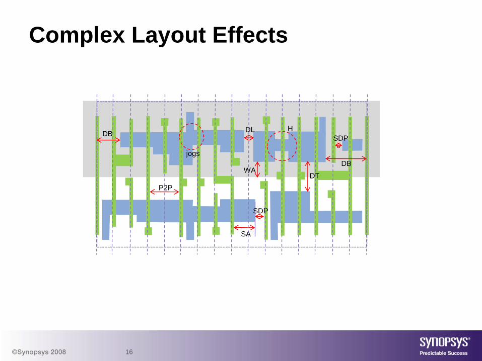
Complex Layout Effects
17
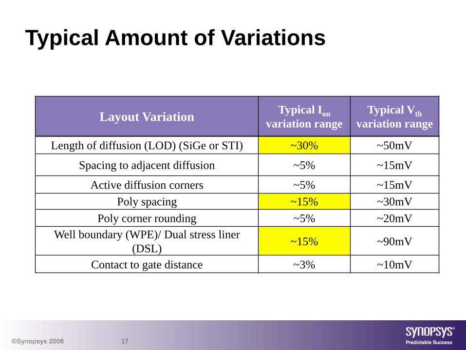
Typical Amount of Variations
Layout VariationTypical Ion
variation range
Typical Vth
variation range
Length of diffusion (LOD) (SiGe or STI) ~30% ~50mV
Spacing to adjacent diffusion ~5% ~15mV
Active diffusion corners ~5% ~15mV
Poly spacing ~15% ~30mV
Poly corner rounding ~5% ~20mV
Well boundary (WPE)/ Dual stress liner
(DSL)~15% ~90mV
Contact to gate distance ~3% ~10mV
18
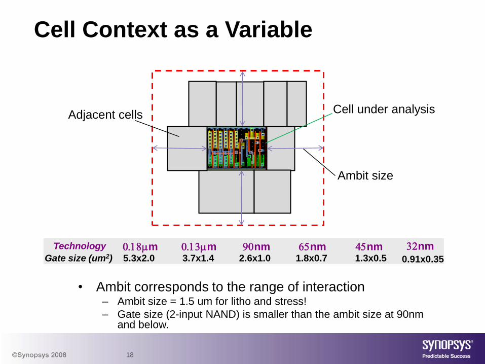
Cell Context as a Variable
• Ambit corresponds to the range of interaction– Ambit size = 1.5 um for litho and stress!
– Gate size (2-input NAND) is smaller than the ambit size at 90nm and below.
Adjacent cells Cell under analysis
Ambit size
3.7x1.4 2.6x1.0 1.8x0.7 1.3x0.55.3x2.0 0.91x0.35Gate size (um2)
32nm0.18m 0.13m 90nm 65nm 45nmTechnology
19
• Introduction
• Modeling Considerations
• Tackling Variability
• Summary
Outline
20
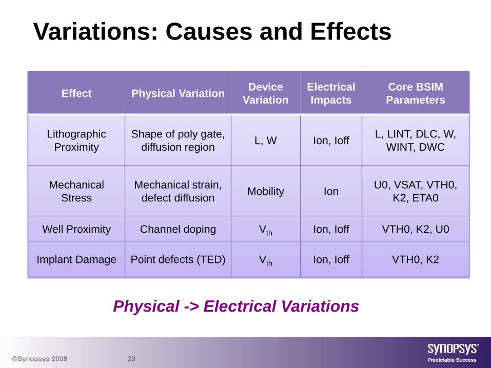
Variations: Causes and Effects
Physical -> Electrical Variations
Effect Physical VariationDevice
Variation
Electrical
Impacts
Core BSIM
Parameters
Lithographic
Proximity
Shape of poly gate,
diffusion regionL, W Ion, Ioff
L, LINT, DLC, W,
WINT, DWC
Mechanical
Stress
Mechanical strain,
defect diffusionMobility Ion
U0, VSAT, VTH0,
K2, ETA0
Well Proximity Channel doping Vth Ion, Ioff VTH0, K2, U0
Implant Damage Point defects (TED) Vth Ion, Ioff VTH0, K2

21
• Empirical Approach
– As good as the test structures
– Critical effects might be overlooked, without
knowing where to look for
• Physics-based
– Better predictability, despite unknowns
– Decoupling of effects
– More efficient usage of test patterns
Modeling Approaches
22
• Increasingly complex proximity effects lead to:– More development effects in LPE and modeling
– Increased runtime during LVS and SPICE simulations
Adapting to Complex Proximity Effects
Co
re m
od
el +
Pro
xim
ity E
ffe
cts
Schematic
Layout
LVS
Annotated Netlist
Simulations
Shared
library
Core
Model
API
d)
Base
runset a)a)
Core
Model L, W
BSIM4.0
BSIM4.6
Exte
nd
ed
layo
ut p
ara
me
ters
Base
runset
LOD
WPE
b)
Core
Model
LOD
WPEb)
Base
runset
LPE
functions
c)
Core
ModelMacro
modelc)
LPE SPICE Modeling
23
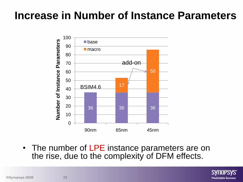
• The number of LPE instance parameters are on the rise, due to the complexity of DFM effects.
Increase in Number of Instance Parameters
36 36 36
17
50
0
10
20
30
40
50
60
70
80
90
100
90nm 65nm 45nm
Nu
mb
er
of
Insta
nce P
ara
mete
rs base
macro
BSIM4.6
add-on
24
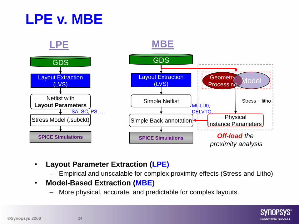
LPE v. MBE
• Layout Parameter Extraction (LPE)
– Empirical and unscalable for complex proximity effects (Stress and Litho)
• Model-Based Extraction (MBE)
– More physical, accurate, and predictable for complex layouts.
GDS
Layout Extraction
(LVS)
Netlist with
Layout Parameters
Stress Model (.subckt)
SPICE Simulations
LPE MBE
GDS
Physical
Instance Parameters
SPICE Simulations
Geometry
ProcessingModel
Layout Extraction
(LVS)
Simple Netlist
Simple Back-annotation
Off-load the
proximity analysis
Stress + lithoMULU0,
DELVTO,
…
SA, SC, PS, …
25
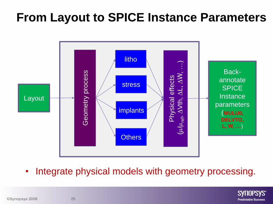
• Integrate physical models with geometry processing.
From Layout to SPICE Instance Parameters
Layout
litho
stress
implants
Others
Geom
etr
y p
rocess
Physic
al effects
(/
ref,
Vth
,
L,
W, …
)
Back-
annotate
SPICE
Instance
parameters
(MULU0,
DELVTO,
L, W, …)

26
Strain Engineering and Modeling
Device
Level
Multi-
Device
Level
Cell
Level
TCAD
TCAD
MBE
Solutions ApplicationsScale
(Physics-based
Compact Model)
(2D/3D FEA)
• Layout dependency
• Process variability control
• Forward looking design rules
• Process optimization
• Device characterization
• Virtual prototyping
• Cell optimization
• Context sensitivity
• Design exploration
(2D/3D FEA)

27
Contour to Electrical Analysis
i
ii
i
dsds WLII ),(
,...),( eqeqds WLI
Litho
Contour
(from Litho Simulator)Weq
Leq
Annotated
Spice
Netlist
Calculates
Equivalent
W & L, etc.
28
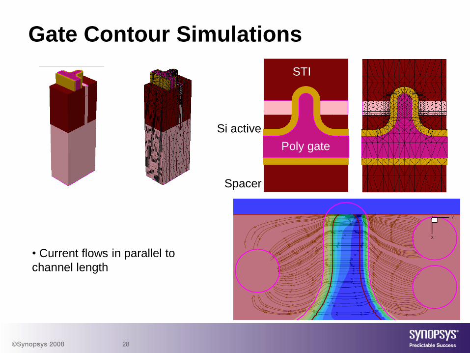
Gate Contour Simulations
Poly gate
Spacer
STI
Si active
• Current flows in parallel to
channel length

29
• Poly flare-out is beneficial
• 10% Ion gain at a fixed Ioff or 3x reduction in Ioff
Non-Rectangular Poly Gate Shape
Threshold voltage
0.00
0.05
0.10
0.15
0.20
0.25
0.30
0.35
-0.02 0 0.02 0.04 0.06 0.08
Vth
[V
]
PY0 [um]
Vtlin
Vtsat
• Average channel
length increasing.
SCE RSCE
DIBL
1.E-10
1.E-09
1.E-08
1.E-07
1.E-06
1.E-05
2.E-05 3.E-05 4.E-05
Ioff
[A
]
Ion [A]
[Rectangle poly]
[Non-rectangular poly]
Ion/Ioff performance
+10%
M. Choi et al. SPIE 09
30
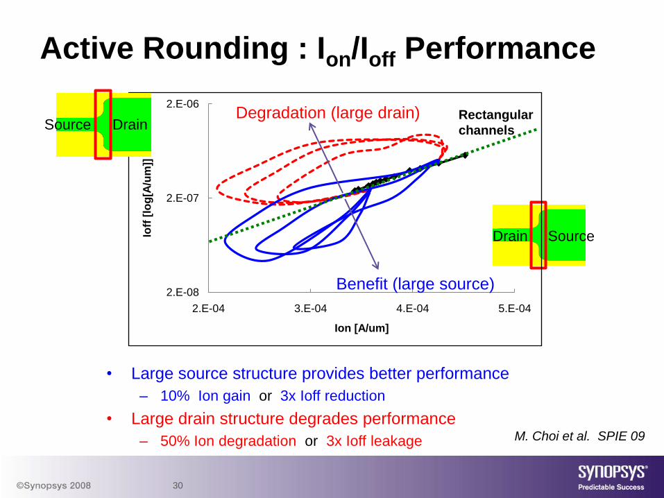
Drain Source
• Large source structure provides better performance
– 10% Ion gain or 3x Ioff reduction
• Large drain structure degrades performance
– 50% Ion degradation or 3x Ioff leakage
Active Rounding : Ion/Ioff Performance
2.E-08
2.E-07
2.E-06
2.E-04 3.E-04 4.E-04 5.E-04
Ioff
[lo
g[A
/um
]]
Ion [A/um]
Rectangular
channels
Degradation (large drain)
Benefit (large source)
Source Drain
M. Choi et al. SPIE 09
31
• Introduction
• Modeling Considerations
• Tackling Variability– Accurate modeling
– Understanding sensitivity
– Prevention
– Optimization
– Visibility to designers
– Margin
– Efficient design flow
• Summary
Outline
32
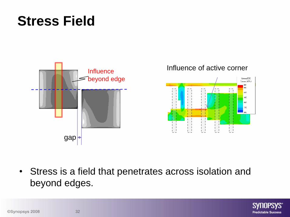
Stress Field
• Stress is a field that penetrates across isolation and
beyond edges.
Influence
beyond edge
Influence of active corner
gap
33
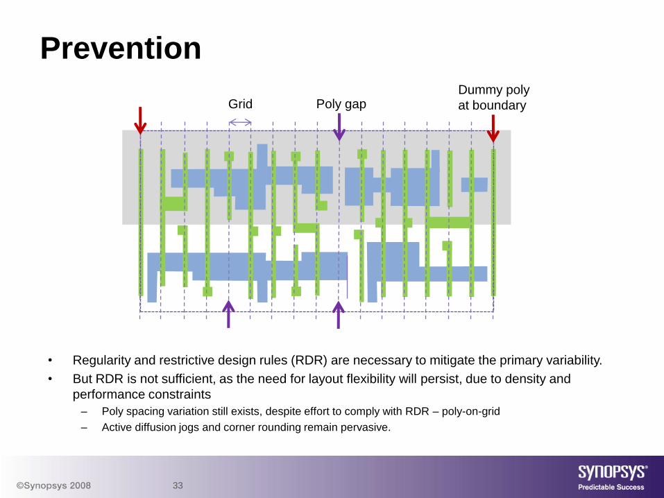
• Regularity and restrictive design rules (RDR) are necessary to mitigate the primary variability.
• But RDR is not sufficient, as the need for layout flexibility will persist, due to density and
performance constraints
– Poly spacing variation still exists, despite effort to comply with RDR – poly-on-grid
– Active diffusion jogs and corner rounding remain pervasive.
Prevention
Poly gapDummy poly
at boundaryGrid
34
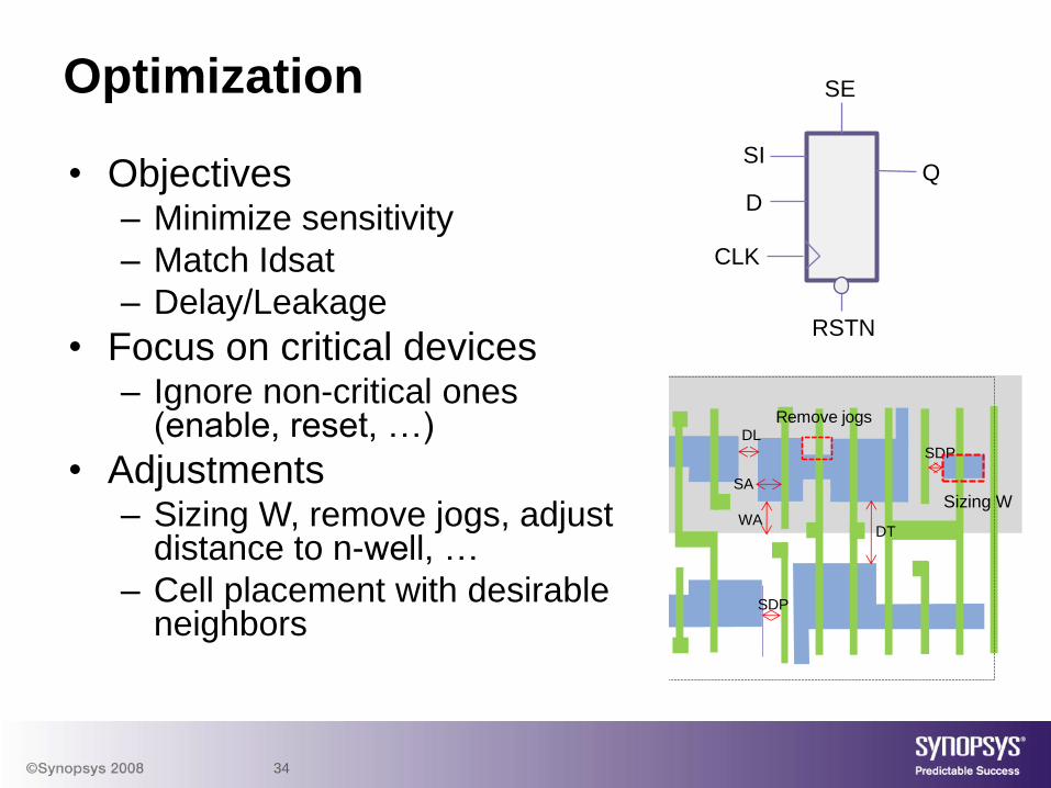
Optimization
• Objectives– Minimize sensitivity
– Match Idsat
– Delay/Leakage
• Focus on critical devices– Ignore non-critical ones
(enable, reset, …)
• Adjustments– Sizing W, remove jogs, adjust
distance to n-well, …
– Cell placement with desirable neighbors
DL
SDP
WA
SDP
DT
Remove jogs
SA
Sizing W
D
CLK
RSTN
SI
SE
Q
35
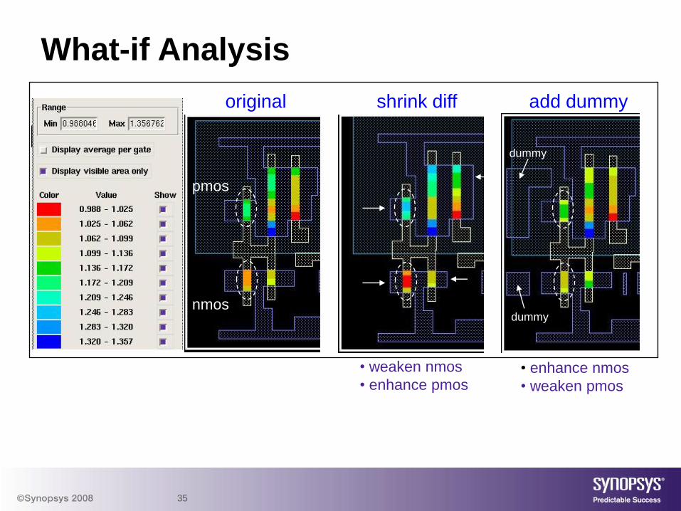
What-if Analysis
original
nmos
pmos
• weaken nmos
• enhance pmos
shrink diff
• enhance nmos
• weaken pmos
dummy
dummy
add dummy
36
Losing Visibility …
• Designers’ questions:– What’s the actual driving strength of transistor M1 ?
– How is M1 different from M2, both having the same W & L?
M1 N_2 N_93 N_9 N_135 pm l=0.032000u w=0.40000u ad=0.048262p pd=1.054000u as=0.028630p ps=0.549000u
nrd=0.534977 nrs=0.233352 ka=0.284000u kb=0.118000u ka1=0.284000u kb1=0.118000u ka2=0.284000u kb2=0.118000u
+ ka3=0.284000u kb3=0.118000u sca=15.009148 scb=0.014816 scc=0.001477 xp=0.244435u
+ xp1=0.230865u xp2=0.174918u xp3=0.191948u xa=0.206750u ka4=0.166915u xb=0.179857u
+ xb1=0.181837u fx=3.862724u fx1=3.855471u fy=0.338502u fy1=0.251403u fy2=0.324598u
+ rs=5.430328u rw=0.634072u *xy(4.047 0.1445)
M2 N_2 N_92 N_9 N_135 pm l=0.032000u w=0.40000u ad=0.042536p pd=1.026000u as=0.028630p ps=0.549000u
nrd=0.533926 nrs=0.233352 ka=0.104000u kb=0.298000u ka1=0.104000u kb1=0.298000u ka2=0.104000u kb2=0.298000u
+ ka3=0.104000u kb3=0.298000u sca=14.969629 scb=0.014816 scc=0.001477 xp=0.140000u
+ xp1=0.140000u xp2=0.140000u xp3=0.140000u xa=0.145771u ka4=0.154446u xb=0.178830u
+ xb1=0.180733u fx=4.010791u fx1=4.004751u fy=0.338502u fy1=0.251403u fy2=0.324598u
+ rs=5.510477u rw=0.634072u *xy(3.867 0.1445)
LPE annotated netlist …

37
From Layout to Electrical …
• Directly relate layout to electrical properties (Ion, Ioff, Vth) for each transistor
in design
MI47 VSS CDN:F67 XI180-NET6:F68 VDD pm l=0.032u w=0.4u ad=0.034174p nrd=0.37971 nrs=0.266667
+ pd=0.678261u ps=0.46u as=0.024p
+ MULU0=1.054 DELVTO=-0.022 $Ion=0.0002595 $Ioff=1.325e-08 $Vtsat=0.069489
Layout MULU0
DELVTO
Instance
Parameters
Ion/Ioff/Vth
Electrical
Properties
MBE
Netlist
Design
38
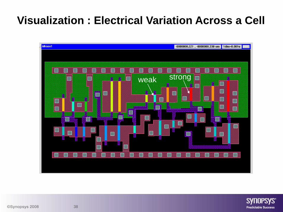
Visualization : Electrical Variation Across a Cell
strongweak
39
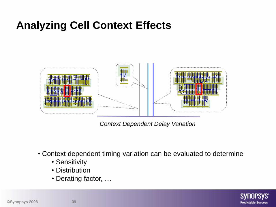
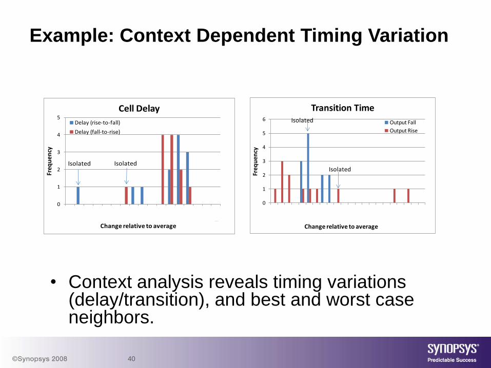
Analyzing Cell Context Effects
• Context dependent timing variation can be evaluated to determine
• Sensitivity
• Distribution
• Derating factor, …
Context Dependent Delay Variation
40
• Context analysis reveals timing variations (delay/transition), and best and worst case neighbors.
Example: Context Dependent Timing Variation
0
1
2
3
4
5
-10
%
-9%
-8%
-7%
-6%
-5%
-4%
-3%
-2%
-1%
0%
1%
2%
3%
4%
5%
Mo
re
Freq
uen
cy
Change relative to average
Cell Delay
Delay (rise-to-fall)
Delay (fall-to-rise)
Isolated Isolated
0
1
2
3
4
5
6
-5%
-4%
-3%
-2%
-1%
0%
1%
2%
3%
4%
5%
6%
7%
8%
9%
10
%1
1%
12
%1
3%
14
%1
5%
Mo
re
Freq
uen
cy
Change relative to average
Transition Time
Output Fall
Output Rise
Isolated
Isolated
41
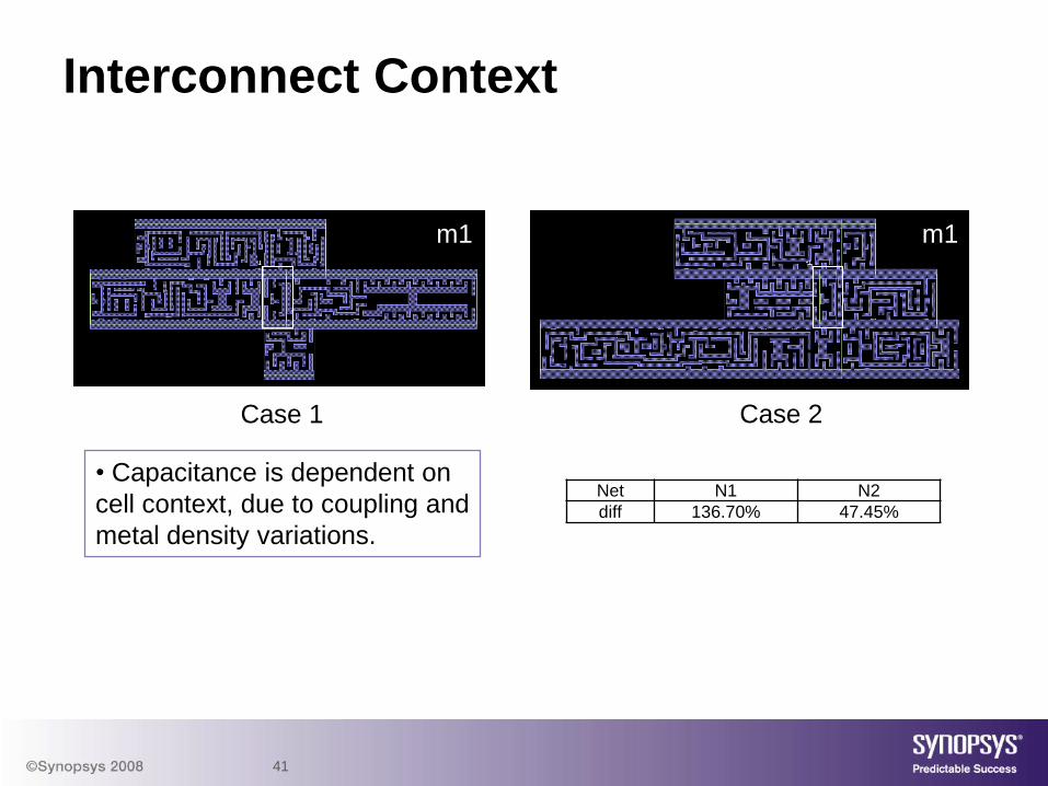
Interconnect Context
Case 2Case 1
• Capacitance is dependent on
cell context, due to coupling and
metal density variations.
Net N1 N2
diff 136.70% 47.45%
m1 m1

42
• Context analysis reveals timing variations, and best and worst case neighbors.
Context Distribution
0
5
10
15
20
25
6.4
5E
-12
6.4
6E
-12
6.4
7E
-12
6.4
9E
-12
6.5
0E
-12
6.5
1E
-12
6.5
2E
-12
6.5
3E
-12
6.5
5E
-12
6.5
6E
-12
6.5
7E
-12
Fre
qu
en
cy
tdelay-fall (s)
0
2
4
6
8
10
12
14
16
18
20
8.7
0E
-12
8.7
3E
-12
8.7
6E
-12
8.7
9E
-12
8.8
2E
-12
8.8
5E
-12
8.8
8E
-12
8.9
1E
-12
8.9
4E
-12
8.9
7E
-12
9.0
0E
-12
Fre
qu
en
cy
tdelay-rise (s)
worstworstbest best
43
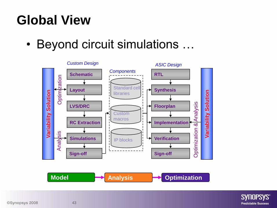
Global View
• Beyond circuit simulations …
Model Analysis Optimization
Standard cell
libraries
Custom
macros
IP blocks
Schematic
Layout
LVS/DRC
Simulations
RC Extraction
Sign-off
RTL
Synthesis
Floorplan
Implementation
Verification
Sign-off
Custom Design ASIC Design
Components
Va
ria
bilit
y S
olu
tio
n
An
aly
sis
Op
tim
iza
tion
Op
tim
iza
tion
& A
na
lysis
Va
ria
bilit
y S
olu
tio
n

44
Open Questions
• Is it possible to standardize the proximity models?
• How to quantify the trade-offs between RDR and design flexibility in actual chips?
• How to take advantage of variability for performance and cost trade-offs?
• How to quickly estimate circuit sensitivity to individual components and their interactions?
• How to perform concurrent optimization to close the design gap between pre and post layout in custom circuits?
• Anything new in FinFET strain engineering?
• …

45
• Layout proximity effects arise from
interactions between design and process
• The stress variability in design surpasses
litho at 45nm and below
• Understanding of the underlying physics is
essential to develop practical solutions to
tackle the electrical variability
• Design methodology and efficiency are
important as well
Summary

46
THANK YOU