Tables of Chebyshev Impedance-Transforming …k5tra.net/tech library/QLP and Lumped LC...
25
Tables of Chebyshev Impedance-Transforming Networks of Low-Pass Filter Form GEORGE L. MATTHAEI, MEMBER, LEEE Summary-Tables of element values are presented for lumped- element Chebyshevimpedance-transforming networks, as are tables giving the Chebyshev passband ripple of each design. These circuits consist of a ladder network formed using series inductances and shunt capacitances; they give a Chebyshevimpedance match between resistor terminations of arbitrary ratio (designs with resistor tenni- nation ratios from 1.5 to 50 are tabulated). The responses of these networks have moderately high attenuation at dc (the amount of attenuation depends on the termination ratio) ; their attenuation then falls to a very low level in the Chebyshev operating band, and then rises steeply above the operating band in a manner typical of low- pass filters. Designs having operating-band fractional bandwidths ranging from 0.2 to 1.0 are given.These impedance-transforming networks can be realized in lumped-element form for low-frequency applications,and in semilumped-element form (such as corrugated waveguide) at microwave frequencies. N GENERAL UMEROUS papers have appeared on the design of quarter-wave step-transformer structures. Among these papers is one by Young, which con- tainstables of designs for quarter-wavetransformers havingChebyshevtransmissioncharacteristics.'Since the accurate calculation of such transformer designs can be very tedious, the existence of extensive tables of step-transformer designs has proved very valuable. Suchtransformersareextremely useful a t microwave frequencies, but for applications involving frequencies much below 1000 \IC, the size of step transformers can become impractically large. Herein tables of element values are presented for a form of lumped-element low-pass filter structure that has impedance-transforming properties similar to those of a step transformer but which can be constructed in very compact form, even at low frequencies. Though it is anticipated that this type of impedance-transforming structure will find greatestapplication at frequencies below the microwave range, it will be seen that the tabulated designs presented here will also be useful as prototypes for the design of semilumped-element im- pedance-transforming networks at microwave frequen- cies. Fig. 1 shows the general formof the impedance-trans- forming structures under consideration. It should be noted that the structure is of the form of a conventional Manuscript received February 12,1964. This research was sup ported by the U. S. Army Electronics Research and Development Laboratory, Ft. Monmouth, X. J., under Contract DA 36-039- Calif. The authoris with The Stanford Research Institute, Menlo Park, Leo You;g, "Tables of cascaded homogeneous quarter-wave transformers, IRE TRANS. ON hlICROWAvE THEORY AND TECH- NIQUE, vol. MTT-7, pp. 233-237; April, 1959. AMC-00084(E). low-passfilter structure. The maindifferencebetween these structures and those of conventional low-pass filters is that conventional low-pass filters have termi- nating resistors of equal (or nearly equal) sizes at each end. In the case of the filters discussed here, the termi- nating resistors may be of radically different size, which means there will be a sizable reflection loss a t zero fre- quency. As a result of this sizable attenuation LA^^ at zero frequency, the transmission characteristics of Chebyshev filters of this type have the form shown in Fig. 2. Sote that there is a band of Chebyshev ripple extending from 0,' to wb', and that above cob' the attenu- ation rises steeply in a manner typical of low-pass filter structures. It should be noted that the attenuation L.4 indicated in Fig. 2 is transducer attenuation expressed in decibels; Le., it is the ratio of the available power of the generator to the power delivered to the load, expressed in db. Xs mentioned above, the designs tabulated herein should prove useful for semilumped-element microwave structures, as well as for lumped-element low-frequency structures. An example of a semilumped-element wave- guide structure is shown in Fig. 3. The structure shown is of thecorrugatedwaveguide filter form's3 in which steps or corrugations in the guideheightare used to simulatetheshuntcapacitorsand series inductors of the structures in Fig. 1. In Fig. 3, where the guide top and bottom walls come close together, the effect is largely like that of a shunt capacitor (as is suggested by the dashed-lined capacitors in the figure). Where the guide top and bottom walls go farapartto form a groove, the effect is predominantly like that of a series inductance (as is suggested by the dashed-line induct- ance in the figure). In this manner, semilumped-element impedance-transforming structures can be designed from the prototype designs given herein. . A structure such as that in Fig. 3 might prove desirable for wave- guide applications, say at L-band or below, where a con- ventional step transformer might be larger than can be accommodated for some given application. Such struc- tures can also find application at higher frequencies for use as structures for coupling to magnetically tunable yttrium-iron-garnet ferrimagnetic resonators. Struc- tures of the form in Fig. 3 have advantages for such ap- IRE, vol. 37, pp. 651-656; June, 1949. S. B. Cohn, "Analysis of a wide-band waveguide filter," PROC. 3 G. L. Matthaei, Leo Young, and E. hl. T. Jones, "Design of Structures,' Stanford Research Inst., Menlo Park, Calif., prepared ?*licronave Filters, Impedance-Matching Networks, and Coupling on SRI Project 3527, Contract DA 36-039 SC-87398, ch. 7; 1963. 939
Transcript of Tables of Chebyshev Impedance-Transforming …k5tra.net/tech library/QLP and Lumped LC...

Tables of Chebyshev Impedance-Transforming Networks of Low-Pass Filter Form
GEORGE L. MATTHAEI, MEMBER, LEEE
Summary-Tables of element values are presented for lumped- element Chebyshev impedance-transforming networks, as are tables giving the Chebyshev passband ripple of each design. These circuits consist of a ladder network formed using series inductances and shunt capacitances; they give a Chebyshev impedance match between resistor terminations of arbitrary ratio (designs with resistor tenni- nation ratios from 1.5 to 50 are tabulated). The responses of these networks have moderately high attenuation at dc (the amount of attenuation depends on the termination ratio) ; their attenuation then falls to a very low level in the Chebyshev operating band, and then rises steeply above the operating band in a manner typical of low- pass filters. Designs having operating-band fractional bandwidths ranging from 0.2 to 1.0 are given. These impedance-transforming networks can be realized in lumped-element form for low-frequency applications, and in semilumped-element form (such as corrugated waveguide) at microwave frequencies.
N GENERAL
UMEROUS papers have appeared on the design of quarter-wave step-transformer structures. Among these papers is one by Young, which con-
tains tables of designs for quarter-wave transformers having Chebyshev transmission characteristics.' Since the accurate calculation of such transformer designs can be very tedious, the existence of extensive tables of step-transformer designs has proved very valuable. Such transformers are extremely useful a t microwave frequencies, but for applications involving frequencies much below 1000 \IC, the size of step transformers can become impractically large.
Herein tables of element values are presented for a form of lumped-element low-pass filter structure that has impedance-transforming properties similar to those of a step transformer but which can be constructed in very compact form, even a t low frequencies. Though it is anticipated that this type of impedance-transforming structure will find greatest application a t frequencies below the microwave range, i t will be seen that the tabulated designs presented here will also be useful as prototypes for the design of semilumped-element im- pedance-transforming networks a t microwave frequen- cies.
Fig. 1 shows the general form of the impedance-trans- forming structures under consideration. It should be noted that the structure is of the form of a conventional
Manuscript received February 12, 1964. This research was s u p ported by the U. S. Army Electronics Research and Development Laboratory, Ft. Monmouth, X . J., under Contract DA 36-039-
Calif. The author is with The Stanford Research Institute, Menlo Park,
Leo You;g, "Tables of cascaded homogeneous quarter-wave transformers, IRE TRANS. ON hlICROWAvE THEORY AND TECH- NIQUE, vol. MTT-7, pp. 233-237; April, 1959.
AMC-00084(E).
low-pass filter structure. The main difference between these structures and those of conventional low-pass filters is that conventional low-pass filters have termi- nating resistors of equal (or nearly equal) sizes a t each end. In the case of the filters discussed here, the termi- nating resistors may be of radically different size, which means there will be a sizable reflection loss a t zero fre- quency. As a result of this sizable attenuation LA^^ a t zero frequency, the transmission characteristics of Chebyshev filters of this type have the form shown in Fig. 2. Sote that there is a band of Chebyshev ripple extending from 0,' to w b ' , and that above cob' the attenu- ation rises steeply in a manner typical of low-pass filter structures. It should be noted that the attenuation L.4
indicated in Fig. 2 is transducer attenuation expressed in decibels; L e . , it is the ratio of the available power of the generator to the power delivered to the load, expressed in db.
Xs mentioned above, the designs tabulated herein should prove useful for semilumped-element microwave structures, as well as for lumped-element low-frequency structures. An example of a semilumped-element wave- guide structure is shown in Fig. 3. The structure shown is of the corrugated waveguide filter form's3 in which steps or corrugations in the guide height are used to simulate the shunt capacitors and series inductors of the structures in Fig. 1. In Fig. 3, where the guide top and bottom walls come close together, the effect is largely like that of a shunt capacitor (as is suggested by the dashed-lined capacitors in the figure). Where the guide top and bottom walls go far apart to form a groove, the effect is predominantly like that of a series inductance (as is suggested by the dashed-line induct- ance in the figure). In this manner, semilumped-element impedance-transforming structures can be designed from the prototype designs given herein. .A structure such as that in Fig. 3 might prove desirable for wave- guide applications, say at L-band or below, where a con- ventional step transformer might be larger than can be accommodated for some given application. Such struc- tures can also find application a t higher frequencies for use as structures for coupling to magnetically tunable yttrium-iron-garnet ferrimagnetic resonators. Struc- tures of the form in Fig. 3 have advantages for such ap-
IRE, vol. 37, pp. 651-656; June, 1949. S. B. Cohn, "Analysis of a wide-band waveguide filter," PROC.
3 G. L. Matthaei, Leo Young, and E. hl. T. Jones, "Design of
Structures,' Stanford Research Inst., Menlo Park, Calif., prepared ?*licronave Filters, Impedance-Matching Networks, and Coupling
on SRI Project 3527, Contract DA 36-039 SC-87398, ch. 7; 1963.
939

940 PROCEEDINGS OF THE IEEE August
, R;+l G;, , RESISTANCE AT END n + l RESISTANCE AT END 0
(a>
G:. l~ ' In t l --- , , ,....+, Rh , CONDUCTANCE AT END n + I
CONDUCTANCE AT END 0
(b) Fig. 1-Definition for normalized prototype element values for im-
pedance-transforming networks of low-pass filter form. (The tabulated element values are normalized SO that go=l and h' = 1. [ S e e Fig. 2 .I)
I I
Fig. 2-Definition of response parameters for low-pass impedance- transforming filters. (The frequency scale for the tabulated proto- type design is normalized so that urn'= 1, as indicated above.)
IUPEDANCE-TRAUSFORUINC CTRVCTYRE
Fig, 3-A corrugated-waveguide structure for matching between guides of different heights.
plications because the inductive section at the low- impedance end of such a structure (forming L4 at the right end in Fig. 3) provides needed room for locating a ferrimagnetic resonator while at the same time giving the impedance transformation required for obtaining tight coupling to the ferrimagnetic r e ~ o n a t o r . ~
PARAMETERS OF THE ATTENUATION CHARACTERISTICS
The frequency scale of the networks tabulated here has been normalized as indicated in Fig. 2 so that the arithmetic mean-operating-band radian frequency,
Wa' + Wb' Wm' = 1
2 (1)
is scaled so that
Wm' = 1.
Herein the frequency variables and element values of the normalized prototype circuits will be primed to indi- cate that they are normalized, and corresponding un- primed quantities will be reserved for the same param- eters scaled to suit specific applications. With the nor- malization in ( 2 ) ,
and w
Wb' = 1 +- '
2 ( 3
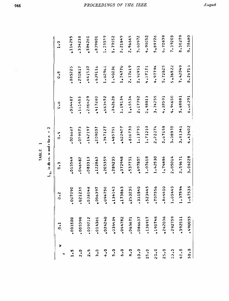
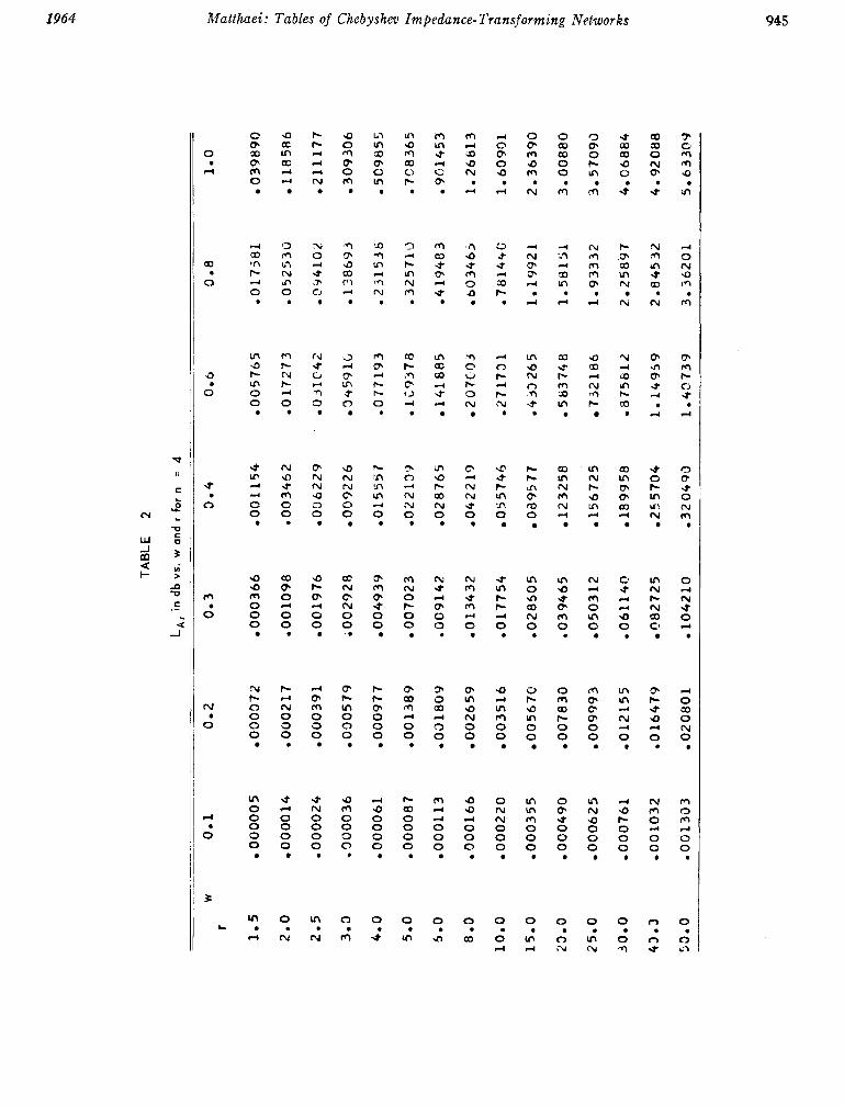
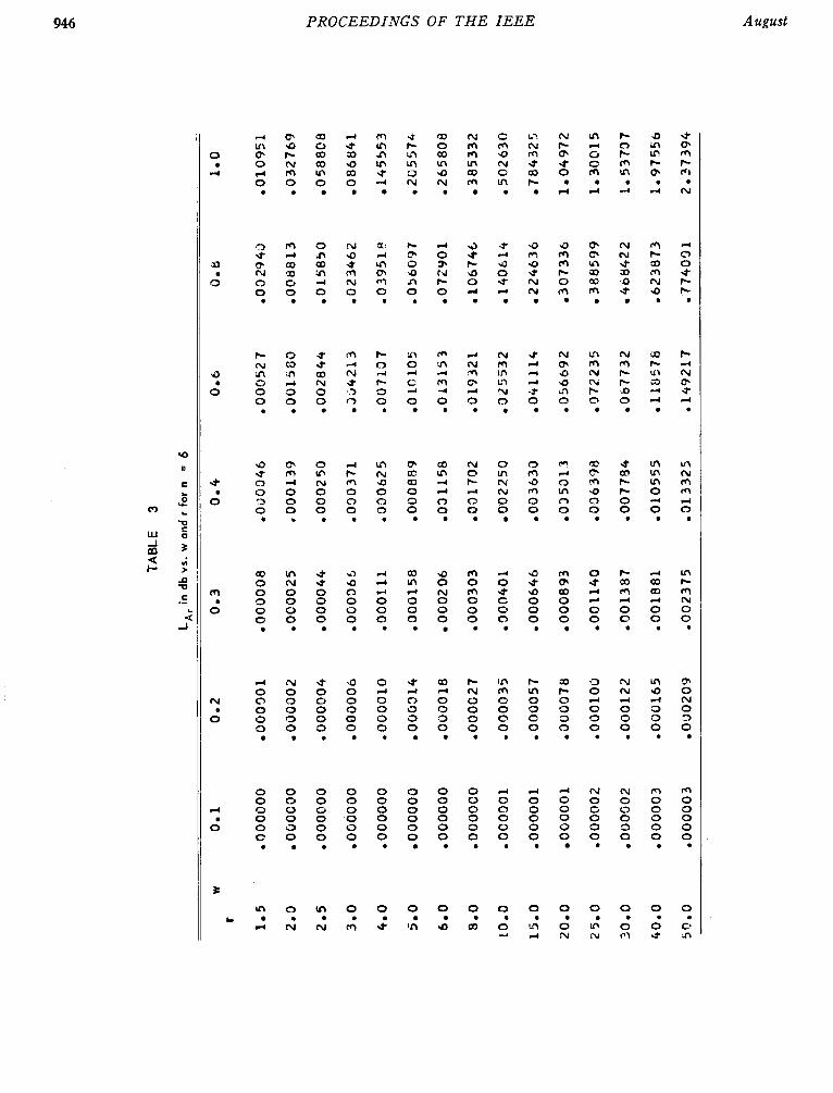
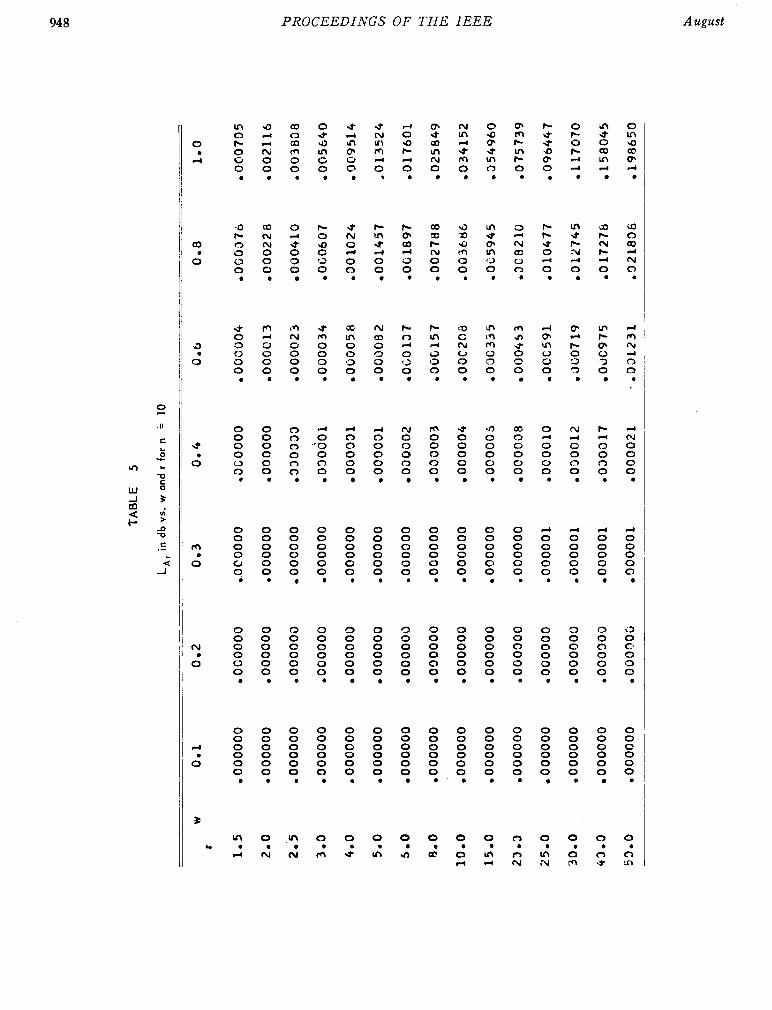
In most impedance-transformer applications, the pa- rameters of the normalized prototype circuit that will be of importance are the impedance or admittance transformation ratio r (see Fig. l ) , the fractional band- width w , and the db passband attenuation ripple Lar (see Fig. 2 ) . After a designer has determined the value of r , the minimum value of w, and the maximum allow- able value of Lar for his application, the next step is to determine the number n of reactive elements required in the circuit in order to meet these specifications. The required value of n can easily be determined with the aid of Tables 1 t o 5 (pp. 944-948). For example, suppose a designer desires an impedance transformer to give an r = 3 impedance ratio over the band from 500 to 1000 Mc with 0.10-db or smaller attenuation ripple ratio in the operating band. The required fractional bandwidth is given by
f b - fa - 2 ( f b -fa) -w=-- 1 (6) f m . f b + f a
4 G. L. Matthaei, et al., "Microwave Filters and Coupling Struc- tures,'' Stanford Research Inst., Menlo Park, Calif., Final Rept., SRI Project 3527, Contract DA 36-039 SC-87398, Sec. 111; February, 1%3.

1964 Xatthaei: Tables of Chebysheo Impedance- Transforming Networks
which for this example gives and
2(1000 - 500)
1000 + 500 - - = 0.667.
This value of fractional bandwidth lies between the w=O.6 and w =0.8 values in Tables 1 to 5 , so the w =0.8 value will be used. This will give an operating bandwidth somewhat larger than is actually required, which is often desirable. However, if this is objection- able, the desired bandwidth can be achieved by inter- polating between the values in Tables 1 to 5 in order to determine the required value of n for w =0.667 and LA? sO.10 db, and then interpolating between numbers in the element-value tables (to be discussed later), to obtain a prototype with w=O.667, r =3, and the given value of n. Reducing the bandwidth from 0.8 to 0.667 would mean that a smaller value of LA? could be achieved for given values of r and n.
Assuming that use of w = 0.8 is satisfactory, we deter- mine the required value of n as follows. From Table 1 (which is for n = 2 reactive elements), for w=O.8 and r = 3, we obtain LA? = 0.639 db, which is too large. From Table 2 (which is for n = 4 reactive elements), for w = 0.8 and r = 3, we obtain LA? = 0.139 db, which is still somewhat too large. Finally, from Table 3 we find that for n= 6, Ldr=0.023 db, which is less than the 0.10 db required. Actually, in this case i t is clear that if the fractional bandwidth were reduced close to the w = 0.667 minimum required value, n = 4 reactive elements would be sufficient to give Ladr < O . 10 db.
Besides the fractional bandwidth w and the operat- ing-band-ripple LA? in Fig. 2, other aspects of the re- sponse of the normalized prototype circuit will at times also be of interest. The attenuation L.tdc a t zero fre- quency is given by
L A d c = 10 log10 - ( r + db 4r
where r is again the impedance or admittance transfor- mation ratio.
In some cases it will be desired to determine the at- tenuation accurately over a range of frequencies, pos- sibly for making use of the strong attenuation band of this type of structure above frequency w2. The attenu- ation characteristic in Fig. 2 can be predicted by map- ping the attenuation characteristic of a conventional Chebyshev low-pass filter (which has an equal-ripple pass band from w”=O to w” =@I”) by use of the map- ping function
J’ & - #0’2
A 01’’ -= (8)
where w“ is the frequency variable for the conventional Chebyshev filter,
A = - Wa‘’
2 (9)
94 1
is the frequency in the response in Fig. 2, which cor- responds to w “ = O for the corresponding conventional Chebyshev low-pass filter characteristic. hfaking use of (8) and (9) and the equations for the attenuation of a conventional Chebyshev low-pass filter (see, for ex- ample, Fig. 2 of Cohn5), we obtain
which applies in the “stop” bands O s w ’ sua‘ and wb’<w’< a. In ( l l ) ,
and n is the number of reactive elements in the im- pedance-transforming filter network. In the operating band w: 5 w‘ 5 Wb‘,
A conventional low-pass Chebyshev response for a fil- ter with n” reactive elements maps into a response of the form in Fig. 2 for a filter having n= 2n” reactive elements. The response in Fig. 2 corresponds to an n = 8 reactive-element design. However, this response could be obtained by mapping the response of a corresponding n” = 4 reactive-element conventional Chebyshev filter design, using the mapping in (8). This is because the mapping function in (8) doubles the degree of the trans- fer function polynomial.
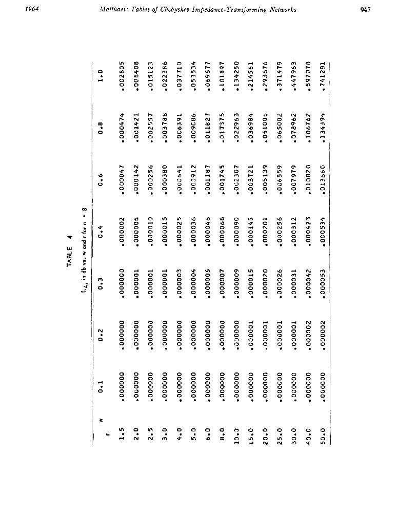
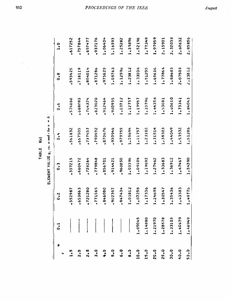
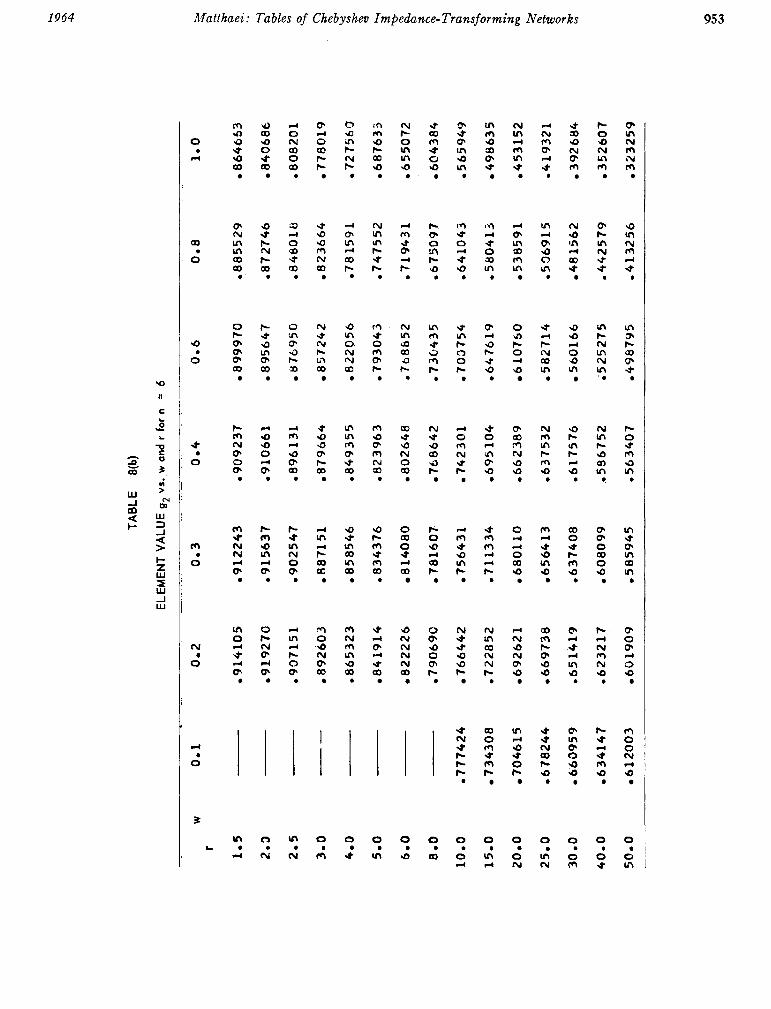
TABLES OF PROTOTYPE ELEMENT VALUES Tables 6 to 10 (pp. 949-963) give element values for
prototype impedance-transforming networks for n = 2, 4, 6 , 8, and 10 reactive elements. After the designer has arrived at values for r , w, and n, the normalized element values can be obtained from the tables. However, since the networks under discussion are antimetric6 (;.e., half of the network is the inverse of the other half), only half of the element values for each network are tabulated, and it is necessary to compute the element values of the second half of the network from those of the first half.
45, pp. 187-196; February, 1957.
and Sons,. Inc., New York, N. Y . , ch. 11 : 1957.
5 S. B. Cohn, “Direct-coupled-resonator filters,” PROC. IRE, vol.
6 E. A. Guillemin, ‘Synthesis of Passive Setworks,” John Wiley

942 PROCEEDINGS OF THE IEEE August
This procedure will now be summarized for each value of n. For n=2 , go= 1, and gl is obtained from Table 6. Then
For n = 4, go = 1 ; and gl and g2 are obtained from Tables 7(a), (b). Then
g3 = g2r, g4 = - 7 and g6 = r. g1 r
For n= 6, go= 1; and gl, g?, and g3 are obtained from Tables 8(a)-(c). Then
g4 = 7 g3
g6 = gzr,
which results in a gradual loss of accuracy as the expan- sion progresses. Thus, values for gl could be obtained with great accuracy, values for g2 with somewhat less accuracy, etc. Tables 6 to 10 include all of the signifi- cant figures that were available in the computer print- out; however, in the case of the values for, say, ele- ments g4 and g5, some of the digits on the right end of each number are doubtless in error. In order to see how serious the errors might be, some responses were com- puted for several designs, including the rather extreme cases of w=O.8, and w = 1.0, having n = 10 and r = 50. The bandwidths were as predicted, and after checking the details of the pass band, the pass band Chebyshev ripples were found to have very nearly the peak values predicted, with a t most two or three units error in the third significant figure and better accuracy in most cases. Thus, though not all of the element values given in Tables 6 to 10 are as accurate as the number of sig- nificant figures shown indicates, the accuracy appears to be more than adequate for typical practical appli- cations.
For n= 8, go= 1; and gl to g4 are obtained from Tables SCALING OF THE NORMALIZED DESIGN 9(a)-(d). Then After a designer has selected a normalized design, the
element values required for his specific application are g6 = g4r, g6 = - j g7 = g21, easily determined by scaling. Let R be the desired resist-
Y ance level of one of the terminations, while R' is the cor- responding resistance of the normalized design. Simi- larly, let wm = (wa+m)/2 be the radian frequency of the
corresponding frequency for the normalized design.
g3
g1 gs = - 9 go = 1.
Y (17) center of the desired operating band, while Wm'= 1 is the
For n = 10, g = 1; and gl to g5 are obtained from Tables Then the scaled element values are computed using lO(a)-(e). Then
g9 = gzr, g1
g10 = - 9 Y
gll = r.
Note that for a design with n reactive elements, there are n+2 element values, go, gl, - . 1 gn, gn+l- Two POS-
sible interpretations of these element values are as indi- cated in Fig. 1. Observe that each of the terminating element values go and gn+l may be either a resistance or a conductance, depending on whether it is next to a shunt capacitance or a series inductance, respectively. This convention is used because it is convenient when applying the principle of duality to the element values. The two interpretations of the element values shown in Fig. 1 actually give the same final circuit for given ter- minations since the circuit shown at (b) could be ob- tained from that shown at (a) by simply turning the circuit a t (a) around and scaling its impedance level.
In carrying out the calculations of the element values in Tables 6 to 10, eight significant figures were carried by the computer. However, the computations were made using a continued-fraction-expansion proCessl6
Rk = Rk' (i) Ck = Ck' ($) R'
where Rk', Ck', and Lk' are for the normalized design and Rk, Ck, and Lk are for the scaled design.
DERIVATION OF THE TABLES The circuit designs given in Tables 6 to 10 were syn-
thesized by first starting with reflection coefficient functions for conventional Chebyshev low-pass filters that have pass bands from w" = 0 to w'' = w1", and have monotonically increasing attenuation above w1". Re- flection coefficient functions for such networks have the form'
problems in network synthesis,n J. Franklin Inst., vol. 249, pp. 189- 7 R. M. Fano, "A note on the solution of certain approximation
205; March, 1950.

1964 Mat thae i : Tables of Chebyshev Impedance- Transforming Networks 943
where 9” = d ’ + j w ’ ‘ is the’complex frequency variable We have not, as yet, discussed how the operating- and the P a k ” and P b k “ give the locations of the zeros band ripple enters into the synthesis problem. It can and poles of the function. Expressions giving the loca- be shown that tions of these poles and zeros for a given circuit com- plexity and Chebyshev ripple amplitude can be found in the literature.’ The poles and zeros of the reflection where coefficient function were then mapped to give the reflec- tion coefficient functions
LA^ 10 loglo (1 + e ) db ( 2 7)
( r - l)?
4r cosh2 [t cosh-l r;)] € = __ (28)
for the desired network. This was accomplished by use of (8) with w” replaced by p”/ j , and w‘ replaced by p ’ / j . The complex mapping function was then (with wl”= 1)
By properly adapting (24) it can be seen that for a given pole location P b k ” = @ , k ” + j W b k ” in the left half of the 9’‘ plane, the corresponding pole locations p b k ’ and a for the p’ plane are given by
~
pbk’, Pbk‘
where
Since ubk” is negative, the argument of the arctangent function is usually negative so that the arctangent is evaluated as between 0 and -a/2 radians. However, since Wbk’’ is sometimes positive and sometimes nega- tive, the argument of the arctangent can go positive in some cases. When the argument is positive, the arctan- gent is evaluated as having a value between -a/2 and -a radians. In this manner, every pole in the I’(p”) reflection coefficient function yields two conjugate poles in the I’(p’) function.
The mapping equations ( 2 5 ) and (26) also apply for mapping the zeros of the I’(p’’) function to give those of the I’(p’) function. The mapping of the zeros is some- what simplified, however, since they lie on the imagi- nary axis in both planes, ;.e., pal;“=jwak“ and Pak’, - P a k ’ = +jwak’.
8 Here p0l ) i s the complex conjugate of p.1’.
is the same E as appears in (11) to (13). Thus, LA^ (and e) are determined by wnt2/.4 (which controls the fractional bandwidth w ) , by r , and by n. Sext , we com- pu te
- 1
sinh-’ ,l/- e
a = (2 9) It - 2
and the parameter n is used in Fano’s’ equations for the pole and zero locations of ( 2 2 ) . By specifying n ” = n / 2 = [number of poles and number of zeros in ( 2 2 ) ] , w1”,
and a , the function in ( 2 2 ) is entirely determined, with the aid of Fano’s results.’
To summarize, the reflection coefficient function I ’ (p” ) , ( 2 2 ) , for a conventional Chebyshev filter is ob- tained from Fano’s paper, using ( 2 7 ) to (29) to fix the value of a to use in Fano’s equations. Sext, the poles and zeros of this function are mapped as discussed in connection with ( 2 5 ) and (26) in order to obtain the reflection coefficient function I’(p’) , ( 2 3 ) , for the desired form of network. This gives I’(p’) in factored form, and its factored polynomials must then be multiplied out so that the numerator and denominator are in unfactored form. Then, using standard methods of network syn- thesis,6 the input impedance function Z(p’) is formed, and the element values g k are obtained by expanding Z(p’) in a continued-fraction expansion.
ACKNOWLEDGMEXT
The mapping in (8) to (10) for use in the synthesis problem described in this paper was suggested to this writer by Prof. H. J. Carlin of the Polytechnic Institute of Brooklyn, N. Y., M. H. Lawton of Stanford Research Institute, Menlo Park, Calif., prepared the IBRl 7090 computer program used in making the calculations for the tables of impedance-matching network designs.
E
TAB
LE
1
LA
, in d
b vs
. w
and
r f
or n
3
2
W
c 1.5
2 -0
2.5
3.0
4.0
5.0
6.0
8.0
10.0
15 0
0
23.0
25.0
3l.
3
4C.O
50.0
-0 . 1
. 00 1800
. 0053
98
-009
712
a014
381
0242
40
0344
34
a044
782
,065
671
a086
637
a 136
917
1907
48
2420
36
-292759
0392
511
a 49
0055
__
_
0.2
. 0070
90
.021
235
-038
143
0563
97
0947
50
134143
1738
63
2532
33
0331
840
a523
445
e737
556
0864
410
1.05445
1 . 37
594
1.67535
0.3
0 15
549
. 0464
82
-083
313
1228
63
2053
59
a289
233
3729
48
a537
751
6978
55
1.07618
1 :425 30
1 74884
2.05014
2.59671
3.08228
0.4
.0266i37
a079
573
0 14
219.
7
2330
37
,347
127
a 48
5751
6224Q 7
ai336733
1.13735
la71
210
2.22374
2.67658
3.38935
3.~
~1
34
1
4.43
402
G -6
a054
487
a161
453
. 2 a64
2 9
417t280
5 63
492
0342
628
1. A9
134
1 65
534
2. G7
792
2 98
813
3.74
255
4.38
531
4. Y4
650
5.88881
6.bt291
0 -8
a065
225
a250
817
a441
537
a 639 1
li.
1.02961
1 . 40
Q3t
1 7
4776
2.37619
2. YZ
95 1
4.37
171
4.97
794
5.72825
5 36
8 22
7. 4
2049
80
2671
4
1.0
1142
95
a334
238
5'0426C
a839
801
1.33539
1 a
79
35
2
2.21849
2.96665
3.60972
409OO52
5 89
726
6.70
839
7.39
203
8 . 50
279
9.38680
TAB
LE
2
W
r
1.5
2.0
2.5
3.3
4.0
5.0
5.0
8.0
10.0
15.0
23.0
25
.0
30.0
43
03
53.0
0.1
0000
05
oOOO
O14
0000
24
.000036
000061
0 00
0087
0001 13
.000166
. 0002
20
-000355
0004
90
0006
2 5
0000761
oOO1
032
-001333
0.2
0000
72
0 00021 7
0003
9 1
0905
79
0009
77
. 00 1389
.Oi)18(19
002659
0035
16
0056
7C
0078
30
0099
93
-012155
0016479
020801
0.3
0003
66
oOO1098
0001976
.002928
. 0049
39
007023
0009142
- 0 13432
,017754
,028605
0039465
0503
12
oO61
140
C'82725
104210
3.4
.001154
0003452
0006229
009226
0015557
002213'9
0028765
-042
219
0557
46
oa9577
123258
156725
199958
25 570
4
-3 2 0493
0.6
0057
65
0 1727 3
o031C42
3459 lI
,
0077
193
. 1 i937R
141 885
2 G7
C'OI
I
.271701
.433265
. 5837
48
732
186
08
75
61
2
1.14959
1.43739
3.8
,017581
.052
530
.994
102
138633
e231536
.325719
.4 19483
ob03465
.78144(;
1. 19921
1.58151
1.93332
2 25897
2.04532
3.36201
1.0
039890
118586
0211117
-309
306
.5C9855
-7C8365
901453
1.26613
1 609r)l
2.36390
3. GO
880
3.57093
4.068~
4 0 92 088
5.633QY
946 PROCEEDINGS OF THE IEEE August
d ln CP 0 rc 0
0
a 4 6 N 0 0
0
r- N v\ 0 0 0
0
9 U 0
0 n a
0
(0
0 0
0 0 0
0
d 0
0 0
c) 3
0 0 0 0 0 C
0
ul
a3 0 W CD In 0
0
0 rn m In
0 4
0
U U
a N 0 0
0
0 v\
0 N
0 0
0
d .t 0
0 0
0
0 d
0 0 0 c)
0
0 0 0 0 0 0
0
In
N
so 0 m ul 9 N
0 3r CJ r- 0
d
0
F m d m
0 4
0
VI O D .
d d 0 0
0
Q 0 N 0 0 0
a 0 0
0 3
d
0
0 0 0 0 0 0
0
0
9 0
0 m 9
0 N
m 0
j.
9 0 U
d
d 0
N h L n U I Y 0
0
0 VI N N 0 0
0
d 0 d 0 P 0
m m 0 0 0
.t CP m
VI r-
N 0
d 0 0
r- rc
0
yc
N 6 B
d
d 0
Lfl N m m d 0
0
In r- m 0 N
0 0
cr, 0 N 0 3 0
m 0 0 0 0 0
0
0
C' 0
.n
m
N QI
9 Q
in
0
d co W d 0 0
0
m 9 d 0 0 0 . m 0 0 3 0 0
0
0
r- 0 0 3 0
0
d 0 0 0 0 0
0
0 N
0 II L.
d 0
ln
r 1.5
2.0
2.5
3.0
4.0
5.0
6.0
8.0
10.3
15.0
20.0
25.0
30.0
40.0
50.0
W
00
1
. 000000
. 0000
00
0 000
000
0 000
000
00
00
00
.ooo
ooo
0 0
00
00
0
. 0000
00
0 0
00
00
0
e 0
00
00
0
. 0000
00
0 000
000
e 0
00
00
0
0 00
0000
. 00000
0
0.2
. 000000
0 000
000
. 000000
. 000
00
0
w 0
00
00
0
0 0
00
00
0
e 0
00
00
0
0 0
00
00
0
. 000
00
0
. OOO
OO
l
- 0000
0 1
0 0
03
00
1
0 0
00
00
1
. 000902
0 0
00
00
2
LA
r in d
b vs
. w
and
r f
or n
8
__
__
0. 3
0 0
00
00
0
00
00
00
1
.00
00
01
. 000
00
1
00
00
03
oOO
OO
O4
e 0
00
00
5
0 000007
0 0
00
00
9
00
00
15
0 0
00
02
0
00
00
26
oOO
OO
31
00
00
42
000053
0.4
0 0
00
00
2
0 0
00
00
6
0 0
30
0
10
eooo
o15
00
00
02
5
00
00
36
e00
00
46
000068
00
00
09
0
e00
01
45
00
00
20
1
e00
02
56
00
00
31
2
e0
00
42
3
e00
05
34
00 6
00
00
47
.DO
0 1
42
,36
02
56
OOG3
80
.303
0641
DC
39 1
2
oOO
1187
00
01
74
5
00
23
G7
00
37
2 1
,00
51
39
,00
65
59
.007
9,79
e 0
10
82
0
e013
66G
__
__
_
0 0
8
00
04
74
000
14
2 1
a0
02
55
7
00
03
78
8
.OM
39
1
009C
86
o0
11
62
7
00
17
37
5
00
22
95
3
00
36
98
4
. 051
00
6
oO65002
.07
89
62
10
67
62
. 134
39
4
10
0
00
28
05
0@
840
8
00
15
12
3
.02
2?
R6
e03
77
10
00
53
53
4
06
95
77
10
18
97
13
42
50
2 1
45
6 1
29
36
76
03
71
47
9
-44
79
63
.
0 5
97
07
8
74
12
91
948 PROCEEDINGS OF THE I E E E August
In
r- 0
0 Q 0
0
r- .€I r3 0 0 d
0
4 0 0
a 0
0 0
0 0
0 0
0 (1)
e
0 0 0 0 0 0
0
0 0
0 0 0 0
0
0 0 0 0 0 0
0
ul
4 d
9
c\r 0 0
0
N 9
N 0 0 0
0
m d =J 0 0 0
0
0 0
C 0
0 0
e
0 0 0 0 0 0
0
0 0 0 0 0 0
0
0 0 0 0 0 0
0
0
N 0
cb a 9 m 0 0
0
0
0 4
0 0
d
8
m N 0
0 0
0 0
0 c)
0 r)
rJ rJ
0
0
0 0
0 0 0
e
0 0 0 0 0 0
e
0 0 0 0 0 0
e
m tu
0
0 3
In 4
G 0
0
I- O 9 0 ‘2 0
e
.t
0 rcl
0
0 3
0
d
-a 0
0 0 0
0
0 0 0 0 0 0 *
0 0 0 0
0 0
0
0 0 0 0 0 0
0
0
m 0
4 * in L 7 0 0
e
4 cu 0 d 0 0
0
Jt In 0 0 A3 0
0
d n 0 0 0 0
0 0 0 0 0 0
e
Q 0
0 0
0 0
0 0 0 0 0 0
0
0
4. 0
4 N Ul m d 0 . r- VI 4- d 0 0
0
N m 0
0 0
e
c3 0 8 0 0
d
0
0 0 0 0 0 0
e
0 0
0 0 0 0
0
0 0 0 0 0 0
0
0
ul 0
0 9 I-
0
d
d
0
I- OI
rl W
a 0
0
I-
d 0
0 (3 0
0
N 0
0 0
0 0
0 0 0 0 0 0
e
0 c)
0 0
0 0
e
0 3 0 0 0 0
0
0
* 0
6 .t W
N in
0 0
W
r- 52
N 0 0
0
r- In
a :> 0
4
0
m 0 0 0 0 0
0
0 0 0 0 0 0
e
0 0 0 0
0 0
0
0 0 0 0 0 0
0
0
oc e
N In rl
m 4
0 e
4
u 9
m 0 0
e
10 C N u 0 0
e
.;t 0 0 0 Q 0
e
0 0 0
0 0
0 0
0 0
0 0
0 0
e
0 0 0
0 0
0 e
0
0 d
e
0 .c OI 4- In D
0
LA 3 L7 In i;)
0 0
Ir\
In
m 0 r J 0
e
.I3 0 0 0 0 0
e
0 0 0
0 0
0 0
0 0
0 0 0 0
e
0 0 0 0 0 0
0
0
d m
0
OI m + in r- 0
0
d 0
ry a2
c) 0
0
m .n
0 0 0
CD 0
0 0
CJ 0
a
0 0 0 0 0 0
0
0 0 0 0 0 0
e
0 0 0 0
0 0
e
r9 0
N n
r- 3
0. 9
0 0
IC r-
0 4.
0 d
e
rl 0. Ln 0 0 0
0
4 0
0 0 0 0
0
rl 0 0 0 0 0
0
0 0 0 0
0 0
e
0 0 0
0 0
0 0
0
In N
e
0
0 IC rl d
e
In 4 r- N
0 d
0
m 4 r- 0 P J 0
e
d N
0 0
0 0
d 0 0 0 0 0
e
0 3
0 0 0 0
0
0 0 0 0 0 0
0
0
0 m
e
0
1 1

TAB
LE.
-6
ELEM
ENT
VALU
E g
, vs
. w
an
d r
fo
r n
= 2
.- .
~~
W
r
1.5
2.0
2.5
3.0
4.0
5.0
6.0
8.0
10
.0
15.3
20.0
25
.0
30
.0
40
.0
50
.0
0.1
,70
62
19
99
87
52
1,2
23
21
1 4
12
45
1,7
29
89
1 9
97
50
2.2
33
28
2.
64
24
5
2.9
96
26
3.
73
69
9
4.3
53
40
4.8
92
87
5.
37
84
5
6,2
37
21
6.9
91
27
0.2
07
03
59
7
99
50
3'7
1.2
18
67
1.4
07
23
1.7
23
45
1
99
00
7
2 2
24
97
2 0
63
26
2
2,9
85
11
3.7
23
09
4.3
37
27
4.
87
46
7
5 . 35
84
4
6 2
14
00
6,9
65
26
0. 3
-69
92
83
98
89
36
1.2
11
1
9
1
39
85
7
1.7
12
89
1 9
77
87
2.2
11
33
2.6
16
48
2.9
66
81
3.7
00
26
4.3
10
67
4.8
44
78
5,3
25
59
6.1
15
90
6.9
22
55
0.4
-69
33
75
,98
05
81
1.2
00
96
1 3
86
75
1.6
98
42
1.9
61
16
2.1
92
65
2.5
94
37
2.9
41
74
3 5
690.
5
4.2
74
25
4.8
03
84
5.2
80
59
6.
12
37
2
6.8
64
06
0.
6
6 7
72
05
09
57
82
6
1.1
73
09
1
35
45
7
1
65
90
0
1.9
15
65
2.
14
17
6
21
53
41
7
2.8
73
48
3.
58
38
6
4.
1751
37
4 0
69
23
7
5.15805
5,9
81
62
6.7
04
78
0 0
8
06
56
53
2
92
84
77
1.1
37
15
10
,31
30
6
1.6
08
17
1
85
69
5
2.0
76
14
2 4
56
52
2.7
85
42
3 -4
74
34
4,0
47
14
4.
54
85
9
5 CO
O30
5.7
98
33
6.4
99
34
1.0
63
24
55
89
44
27
1 0
95
45
1 2
64
91
1
54
91
9
1.7
88
85
2 . 00
00
0
2.
36
64
3
2.6
83
28
3.3
46
64
3 8
98
72
4.3
81
78
4.
81
6
64
5.5
85
70
6.
26
09
9
.. N

950 PROCEEDINGS O F T H E I E E E August
0 0 d
(0
0
5 0
4
0
m 0
N
0
d 0
0
3
b
6 6
N 9
9
4- . *
n OI
0 OL?
0
I
I- 0
0 4-
m
d
W
0- m In N 6
N
d
6 9
L? r- N
0 OD rn 9
N
0 OD In r- In
N
0
0 J'1
b

TAB
LE
7(b)
ELEM
ENT
VA
LUE
g2
bs.
wa
nd
r f
or n
=
4 . .~
W
@e 1
87
94
38
86
41
80
e 8
32
36
0
80
14
75
07
49
72
@
70
92
1
7
06
76
87
2
06
27
77
1
-59
16
27
e 5
30
78
4
e4
91
32
5
46
27
47
44
06
56
04
01
96
2
38
43
2 5
00
2
0 R
77
47
3
86
1
0 50
82
86
80
07
97
39
6
74
49
53
e 7
04
05
0
06
71
30
7
06
21
63
5
e 5
85
09
1
52
34
55
e 4
83
4
17
04
54
38
0
e4
31
89
9
0 3
98
57
4
37
44
22
0.3
0 8
73
99
0
85
60
62
e 8
22
70
1
-79
06
97
07
37
20
5
e 6
95
54
8
66
22
16
06
11
64
0
57
44
12
5 1
15
33
47
06
04
44
08
6 3
04
17
79
9
38
35
34
03
58
63
8
0.4
86
90
73
84
90
9 1
81
43
92
07
81
40
8
07
26
51
5
6R 3
85
9
06
49
75
1
e 5
98
00
2
05
59
89
4
e4
95
45
7
45 3
44
2
04
22
86
9
39
91
29
e 3
63
81
7
03
38
12
9
0.6
08
54
89
4
08
29
35
1
-79
11
12
0 7
55
57
3
69
71
04
06
51
96
6
06
15
97
8
e5
t14
85
05
21
41
3
04
53
74
2
40
97
04
0 3
77
73
5
03
52
98
5
e 3
16 3
49
02
89
89
8
0-8
83
48
8C
80
24
63
e 7
60
00
9
-72
15
36
e6
59
16
2
e 6
11
49
3
57
37
22
e 5
16
88
4
04
75
37
3
04
05
94
4
036
13
56
32
93
78
30
48
98
26
91
9
6
,24
3R
86
10
0
80
94
1 4
e 7
69
79
4
*72
32
14
e6
82
05
6
6 1
64
5 1
56
70
04
52
81
95
47
04
3@
e 4
28
76
2
03
60
21
2
e 3
17
07
4
e 2
86
63
2
26
36
34
e230
600
20
75
63
TAB
LE
8(a)
ELEM
ENT
VALU
E g
, vs.
wa
nd
r f
or n
- 6
-
-
W
r
1.5
2.0
2m
S
3.0
4.0
5mO
6.0
8.3
10.0
15.0
20.0
25
.0
30.0
40
.0
*53.
0
0.1
~
1 0
50
45
1.1
48
80
1.2
19
70
1 2
85
78
1.3
31
03
1.4
04
79
1 4
69
49
0.2
55
29
87
-65
38
63
72
12
80
07
71
56
5
84
60
80
09
02
35
7
. 947
43
6
1.0
18
12
1 0
72
58
1.1
73
36
1.2
46
98
1 3
05
47
1 3
54
36
1.4
33
83
1 4
97
76
0.3
55
72
1
5
66
04
72
. 7282
64
. 779
84
8
85
67
01
9 1
44
2 1
96
08
50
1.0
33
96
1.0
91
04
1 1
96
92
1.2
74
62
1 3
36
83
1.3
89
12
1 4
74
67
1.5
43
90
0.4
56
18
32
,65
75
05
, 73
74
5 7
*79
06
92
87
06
76
93
09
46
. 9737
55
1.3
56
94
1.1
17
57
1.2
31
02
1.3
15
14
1.3
83
03
1.4
40
49
1.5
35
32
1.5
12
86
0 06
5 7
48
66
68
80
83
764324
82
30
20
9 1
24
64
.9a
o9
35
1.0
37
1
2
1.1
27
37
1.1
99
57
1 3
37
96
1.4
43
56
1 5
30
8 1
1.6
06
10
1 7
33
4.1
1. t
1404
3
Om
8
05
93
42
5
07
18
11
9
80
40
14
m87
1286
09
75
82
9
1.0
57
63
1.1
25
90
1.2
38
12
1,3
30
06
1-51
205
1.6
56
16
1.7
78
64
1 8
86
85
2.0
75
03
L 02
38 1
2
1.0
e6
17
25
2
0 7
57
84
4
. 857
47
7
-93
71
76
1 0
64
04
1.1
65
93
1.2
52
82
1 3
98
96
1.5
21
96
1 7
73
48
1.9
79
59
2.1
59
01
2.3
20
38
2 0 6
06
32
2.8
58
56
0
II
b
TAB
LE
8(b)
ELEM
ENT
VA
LUE
g2
vs.
w a
nd r
for
n
3 6
-
-.
W
r 1.5
2.0
2.5
300
40 0
500
6.0
BO
O
10.0
15.0
2000
2500
30 0
0
40
.0
50
.0
0-1
0777
424
7343
08
7046
15
0678
244
6609
59
0634
147
6 12003
0-2
-914
105
.919
270
o937
151
e 89
2603
0865
323
84 19 14
e 82
2226
e 790
690
7664
42
0722
852
6926
2 1
e 66
9738
o651
413
0623
217
60 19
09
0.3
-912
243
,915
637
0902
547
8871
51
e 85
8546
e 834
376
8 14
080
e 78
1607
7564
31
0711
334
6801
10
e656
413
0637
408
6080
99
-585
945
0 04
0909
237
0910
661
0896
131
0879664
0849
355
0823
963
8026
48
e7li8642
a742
301
-695
104
ob62
389
0637
532
0617
576
,053
6752
0563
407
0.6
8999
70
8956
47
8769
50
8572
42
8220
56
7930
43
0768
652
073L
.435
e 703754
0647
619
6 10
750
0582
71.4
5601
66
0.52
5215
0498
7Y5
0.8
0885
529
0872
746
0846
011i
8236
64
078 159
1
0747
552
-719431
0675
097
-641043
- 58041
3
5385
9 1
0536
915
48 15
62
-442579
-413
256
1.0
8646
63
8406
86
0 80
8201
7780
19
e 727560
6876
33
0655
072
6043
84
0565
949
4986
35
0453
152
-419
321
3926
84
e 35
2607
3232
59

08
91
; 'L
682111'9
Lf1198 ' S
2S
69
E'S
LS128 't
E11861 '3
U0
95
3'E
OO
SOT 'E
.
BG
EO
L'Z
47€41+'2
LO
OZ
Z'Z
8SZ
I26'1
29
E5
L'f
L11LSS' 1:
f9c
l1E
't
0 'I
LCE
OL'L
90
2€
6'9
L1ES
C")
36
F4
2'4
ES
EO
O'G
Z4ZL€'11
91
91
9'E
95
94
Z'E
TEE
?IU'2
+/Z
L0
9'Z
ECZ11E'Z
FOF'E
O'Z
€G
CS
8'1
F6
33
9'1
31
€0
E 'I
3' 0
LLLEL'L
10
f96
'9
f8180'9
19l85'5
ETOZO
'S
65
f6E
'11
L811E9'E
ES
EL
2'E
92
84
8'2
82
12
9'Z
LE11SE'Z
L6
EfO
'Z
8E 1
98
' 1
LZ
ES
9'1
9L
68
E'I
€'O
20
*19
1'1
6S
LR
6'9
6E
E0
1'9
f 82
09
'5
S29fO'S
9E
CO
f'f
I; 5 L99.E
2f9
82
'E
89
19
8'2
9L
82
9'Z
ZS
65C-'Z
ZE
6fO
'Z
OfL
98
'I
L471159'1
68
16
E'l:
2'0
0'c
5
0'011
O'C
E
OL
SZ
O'O
Z
0'5
1
C'C'I
0'8
0 '9
0'5
0'11
O'E s '2 c '2
5.1:
1
M
9 =
'01 J PuD M
*SA
3
fllVh
lN3W313

k
TAB
LE
9(a)
ELEM
ENT
VALU
E g
, vs
. w
an
d r
for
n
= 8
~~
0.1
0.2
.a4
13
23
83
23
32
0‘32 12
26
09
45
45
0
e9
30
52
3
1.0
25
65
0.3
e4
55
71
9
e 5
43
59
0
05
87
67
6
06
19
46
8
-66
92
24
70
59
26
07
32
73
1
07
76
12
4
8C
89
62
-86
81
51
0910899
. 944
4 3 0
e9
72
20
9
1.0
16
91
1.05
225
0.4
047d895
o5
51
57
5
e5
98
01
5
06
,32
42
4
06
R2
21
3
.71
a~
5a
07
47
99
4
07
93
19
3
;827
842
e8
91
98
7
09
36
72
1
097 28
53
1.?0
293
1.3
51
51
1.33063
G 08
05
14
19
7
.6c7
2034
. 660
08
:-
. 704
2
59
e 7
70
92
9
.E2
12
32
o862435
.928134
o9
8G
42
1
1.(
83
28
1.1
Sh
Oi
1.2
18
5t
1.2
72
47
1. 3
63
st,
1. 4
43
07
1.0
54
22
03
.rj4
42
73
7 1
36
92
. 767649
Oi3
53P
8E
91
56
41
.969
54cI
1,05
775
1.12
99?
1.27
253
1.3
b5
42
1.4d
139
1 .-
5662
3
1 7
13
87
1. P
41
95

TAB
LE
9(b)
ELEM
ENT
VALU
E g
2 v
s. w
and
r f
or
n 8
W
0.1
r
le 5
2.0
2- 5
3.0
4.0
5-0
6- 0
8.0
10.0
15-9
20.0
25
.0
33.3
43
.3
59.0
0.2
8448
24
-823
343
8 10
364
e799
795
e 77
9936
764694
0-3
e 88
2869
e 91
2871
,915
840
e913
547
-904
478
8944
60
e885
792
e869
951
8568
85
-831
899
,813
252
-798502
7862
99
7668 16
-751
629
0.4
-891
d26
e91
13
77
- 91 2 53
7
9389
4 1
warn
0887
791
8779
0 1
-860
801
8466
73
-819
587
e739
578
e793709
-770
575
-749
599
-733
139
0.6
e 86
9498
e904
2Cb
9Gl8
33
8314
61
-88Cb613
e 86
652 3
e 85
3892
.a32
512
e 8 E424
e 76
1 8
1 7
7 57
42 0
-738
122
-722
152
e695
624
e176535
0 -8
s 883
542
.a91146
8 8 33
2C
e872
552
8508
8.9
-831
597
-8 147
63
-786810
e764
262
e721
839
,691
015
6666
87
-546
623
e614
591
iE95
3.3
1.0
-872284
e 86
9198
e 85
3352
e836
225
8048
66
e 77
8309
e755
688
,718
858
5896
24
-635
568
5967
77
5665
79
-541
899
0 5 s39
7 3
4731
73
b

TAB
LE
9(c
)
ELEM
ENT
VALU
E g
3 v
s. w
an
d r
for
n
= 8
-.
~~
__
__
__
_.
W
~.
~ .
~..__
0.1
0.2
0.3
0.4
0.6
r
1.5
2.0
2.5
3. 3
4.0
5.0
6.0
8.0
1 . 25
93
4
1 4
56
45
1.58
652
1.68
459
1 0
56
05
1.9
97
83
2 1
09
95
2.30
736
1.2
96
12
1.4
65
26
1.5
91
25
l.bY
517
1.8
62
95
2,3
03
32
4.11831
2,3
17
04
10
.0
-2.4
7012
2.482
53
2
.51
53
3
15.3
2.71
634
2.
7933
0 2
ob
14
25
2.8
68
67
23.0
3
32
60
4
3
.G5
09
3
3.07750
3.1
51
54
3.7
22
55
3 . 77
99
3
3
.62
87
7
3.3
69
99
50.0
4.0026
1
4.0
51
98
4.1
12
34
4.2
63
06
___
0.8
1
.0
1 2
78
92
1,4
50
62
1.5
81
13
1.6
90
43
1.8
71
63
2. C
22
37
2.1
52
74
2.3
75
46
2.56429
2 .*
349 3
7
3.26
139
3.5
29
27
3.76730
4.1
wa
9
4.5
3P
70
1.2
64
86
1 4
4120
4
1 5
75
54
1 6
90
26
1.88
272
2.04
432
2.18
591
2.4
29
66
2.63
6544
3. C7037
3.42
553
3.73
421
4.G
lrJ6
4
4.49
736
4. 9
2336
x
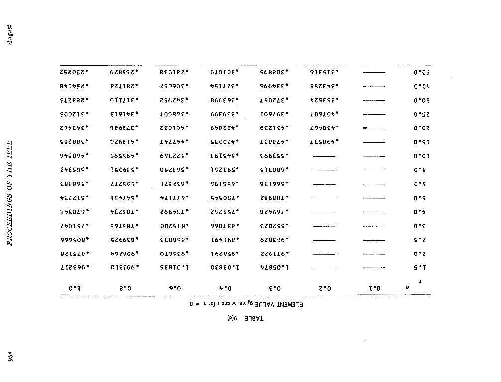
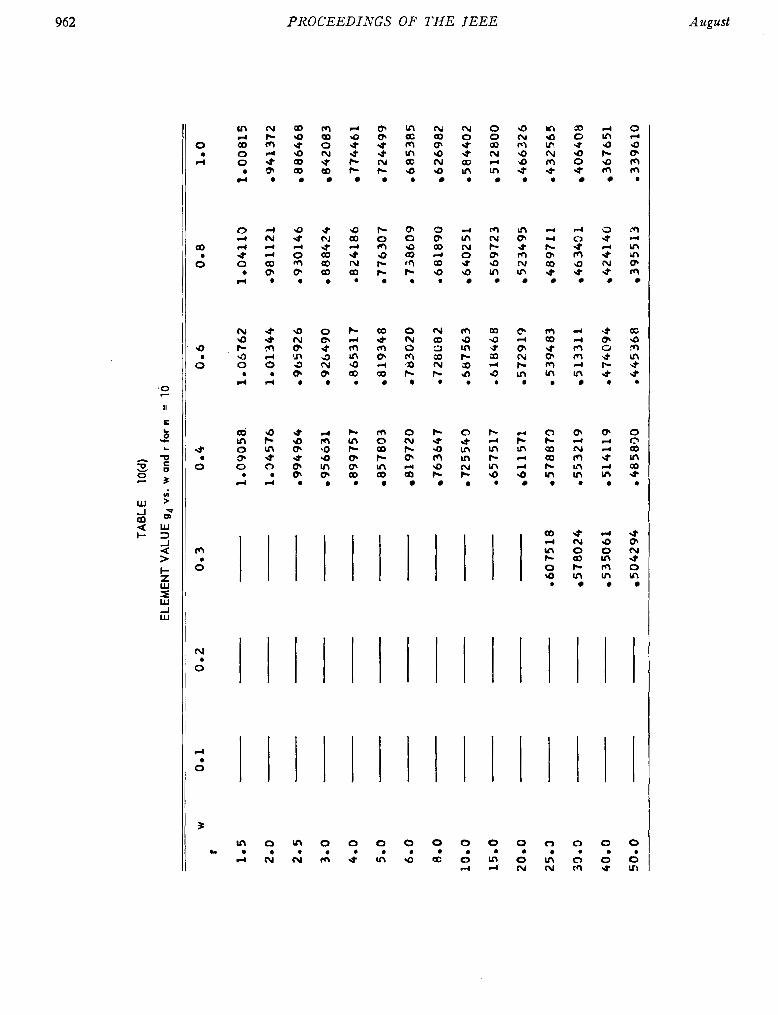
TABLE 9(d)
ELEMENT VALUE g4 vs. w and r for n = 8
W 001 002 0.3 00 4 0.6 0 08 1.0 c
2.0 ,971922 0958291 9'36G7 0 908264 e875128
2.5 oYC.3029 0891491 rt368633 839925 805666
3.0 0852023 a 837866 08 15200 0785765 0751047
4.0 0769428 0758252 734992 0705234 670348
5.0 e 708982 0 730545 0677174 64743 1 0612734
5.3 -666138 -656 195 632 871 ob03277 m568883
800 0 60031 5 0591251 565250 0539351 505343
10.0 - 0 553993 0 545193 522369 493595 a 460 546
15.0 498537 ,478837 . 473935 0447747 0419926 a388285
20.0 - -438467 -431239 42 2 849 o401C32 373988 343462
25.0 -.. 407607 e397601 0399399 0366907 341613 0 3 12C03
50.0 .3n3524 372057 . 35 3998 3.i2952 .3171.10 0288273
45.3 e343258 334996 0327154 a306662' .28 1728 m254148
53.0 0315316 308895 30 1679 -281038 25682Y . 230252

TAB
LE
lO(a)
ELEM
ENT
VALU
E g,
vs.
w a
nd r
for
n
=
10
._ ~~
.
~~~
. ~
__
__
__
__
_~
W
.~ ._
~
.
~~
. ..__
0.1
0.2
0.3
0.4
0.6
O*A
1.
0 c 10s
0411731
431653
-451413
-480211
2.0
0452862
-488315
o5164YfS
5572
40
2.5
05
30
63
0
5242
48
-5
5821
6 607974
3.0
5249
50
. 5 507
95
05
8932
1 06
4653
1
4.0
05
58
05
2
5692
42
53519 7
7046
35
5.0
0531
406
.6
1738
0 66
922 5
0748
736
6.0
0632
333
ob
3961
3
0696
516
0784
761
8.0
63333.3
.47339
7 39
29 5
8424
69
10.0
0634
913
07Z0257
7 72
676
15.0
6953
35
743 24
6 0834819
. 8885
93
9771
72
23.3
0724
629
o7
8287
8
o88G
786
1 04
508
55
.0
a717
659
-7
4679
3 810293
9 1
79
03
1.10145
30
.0
0736
946
076510i)
0833
156
,9
4935
0 1
1503
3
40.0
7669
02
e7
9483
9 087C4277
loi30139 1
. 23350
50.0
7899
86
81
832
5 96
0G56
1
04409
1. 303
94

t-4 h
h
kl
TAB
LE
10(b
)
ELEM
ENT
VALU
E g
2 vs
. w
an
d r
for
n
= 10
c W
1.5
2.0
2.5
3.0
4.0
5.0
6.0
3.3
10.0
15.0
20
.0
25
. 0
so. 0
40
. 0
53.9
0.1
0.
2 0.
3
a 8
72
60
8
86
61
48
. 855
48
9
84
68
63
e8
5 1
50
4
08
81
63
0
89
44
02
-89
89
63
-90
12
33
n9
00
48
9
-89
84
23
08
93
31
2
08
88
54
5
o8
77
50
9
08
68
17
3
me6
0536
08
53
92
6
09
42
72
5
0833681
0.6
85
86
25
88
47
12
08
92
59
4
89
48
96
08
93
78
7
08
90
21
5
08
85
03
6
87
76
54
8 6
99
6 9
a 85
3825
8 4
39
50
83
02
58
08
21
09
2
.8i4
5899
. 793
53
3
08
60
76
7
08
R1
90
1
88
56
95
8.84
5 6
1
08
77
95
9
87
00
70
86
23
20
e3
48
23
2
8 3
60
18
0 1
14
67
07
92
44
9
07
76
87
5
76
36
44
07
41
88
9
07
24
33
3
85
97
01
87
23
99
86
94
71
86
28
17
84
74
90
08
32
82
4
a 8
19
52
6
07
96
64
5
77
75
67
-74
04
19
,71
23
55
.6@
97
06
06
70
66
6
06
39
71
2
6 1
49
90
0
“rl
b
e os
E x
b
Et 0.s f
TAB
LE
lO(c
)
ELEM
ENT
VA
LUE
g3
vs.
w and
r fo
r n
- 10
. .-
__
_
-
W
r
1.5
2.0
2. 5
3.0 4.3
5.0
6.0
8.3
10.0
15.0
20.0
25.0
33.0
40.0
53.3
0.1
0.2
Om 3
-
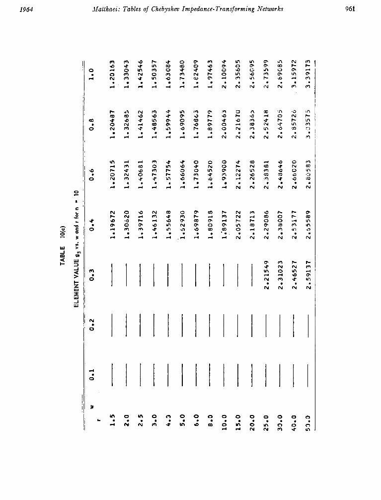
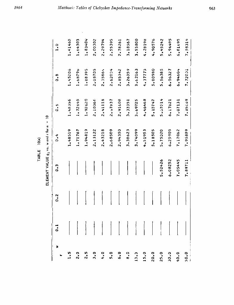
2.21549
2.31023
2.46527
2.59137
0.4
1.19672
1 30620
10 39716
1.46132
1 55648
1.52930
1.69879
1.60918
1.-89137
2.05722
2. 18713
2.29086
2 38
00'1
2.53177
2.55589
0.6
1.20715
1.32431
1.4068 1
1.47303
1. 57
754
1 66
064
1 73
040
1.64520
1 939GO
2.12274
2.26528
2.38381
2 48646
2.66020
2.8i15R3
0.8
1 2
04
87
1.32685
1.41462
1 48563
1 59944
1.69095
10 76
863
1.89779
20 004
63
2.21670
2.38365
2.52418
20 647
05
2.85726
3.33575
1.0
1.20163
1 33043
1.42546
1.50357
1 63084
1.73480
1. e2409
1 97463
2 0 10094
20 356
05
2056C95
2073599
2.69085
3. 15972
3.39173
TAB
LE
10(d
)
ELEM
ENT
VA
LUE
g4
vs.
w a
nd
r f
or n
=
10
__
__
W
r
1.5
2.0 2.5
3. 0
4.0
5.0
6.0
8.0
10.0
15.0
20.0
25. 3
39.3
40
.0
50
.0
0.1
0.2
0.3
a607
518
5780
24
5350
61
5042
94
0.4
1.09058
1.34576
0994
964
-956
031
0899
757
0857
803
81
972
0
7636
47
0725540
-657
517
61 1 571
e578
873
0553
219
0514
119
e 4
85
83
0
0.6
1.06762
1.01344
w963
926
0926
490
0865
317
8193
48
07ir
3020
o728
C82
,587
563
0618
468
-572
919
. 5 394
83
5133
1 1
,474
094
e445
368
0.8
1.04110
098
11
21
0930
146
0 888
42G
0824
186
0776307
a730
609
0681890
6402
51
5 697
2 3
5234
95
4897
1 I
46 34G 1
4241
40
3955
13
1.0
1.00815
0941
372
8864
68
8420
83
7744
6 1
0724
499
,685
385
6269
82
0584
402
5128
00
0466
326
04
32
56
5
4064
08
3676
51
,339
610
c,
TAB
LE
1 O(e)
ELEM
ENT
VALU
E g
5 vs
. w
ond
r f
or
n =
10
r
__
___
___
-
W
r
1.5
2.0
2.5
3.0
4.0
5.0
6.0
8.3
11.2
15
.0
20
.0
25.0
33.0
40.0
50.0
0.1
0
.2
0.3
5.5
24
26
6.0
82
52
7.0
54
45
7.
89
71
1
0.4
1.4
85
19
1.7
17
67
1.9
48
19
2.13122
2.4
32
18
2.6
85
09
2.9
43
50
3.38
62.3
3.7
40
99
4.5
19
53
5.1
85
05
5.7
53
20
6.25905
7.1
70
62
7.95889
C.p
1.4
03
56
1 7
26
45
1. 9
26
20
2.10366
2.4
11
18
2.07837
2 91608
3.3
33
51
3.6
97
25
4.4
64
68
5 1
37
47
50
37
01
4
60 1
75
21
7.0
71
31
7.8
5L
69
1.0
1 4
14
60
1 6
43
03
1 8
34
04
'
2.0
03
02
2 2
97
94
2.5
53
95
2.7
82
61
3.1
85
67
3.53800
4.2
81
96
4.9
05
76
5.4
52
42
5.9
44
95
6.81695
7.5
53
14


![Interpolación - unican.es€¦ · Interpolación de Chebyshev Interpolación de Chebyshev Interpolación de Chebyshev Dada una función f(x) definida en un intervalo [a;b], la mejor](https://static.fdocuments.in/doc/165x107/5ea02ee04f178c0f894b75f7/interpolacin-interpolacin-de-chebyshev-interpolacin-de-chebyshev-interpolacin.jpg)