
TABLE OF CONTENTS - Repeater Builder OF CONTENTS ... Controls: All controls for normal operation are...
22
TABLE OF CONTENTS General Description ................................................................................................... 1 Guaranteed Minimum Performance ........................................................................... 2 Operating Instructions ................................................................................................ 3 Block Diagram ............................................................................................................ 4 Circuit Description ...................................................................................................... 5 Receiver ............................................................................................................ 5 Frequency Control ............................................................................................ 6 Channel Selection ............................................................................................. 6 ,~Iignment .................................................................................................................. 7 Troubleshooting ....................................................................................................... 10 Troubleshooting Chart ..................................................................................... 12 Voltage Chart .................................................................................................. 13 Integrated Circuits Chart ................................................................................. 14 Semi-Conductor Pin Identification ................................................................... 17 Diagrams & Schematics Parts Lists TCXO .............................................................................. 18 ................................... 20 Mixer ................................................................................ 21 ................................... 22 Receiver Multiplier ........................................................... 24 ................................... 26 I.F .................................................................................... 28 ................................... 27 Squelch ........................................................................... 30 ................................... 32 Receiver Audio ................................................................ 34 ................................... 33 Master Interconnect ......................................................... 36 ................................... 38 Front Panel ..................................................................... .40 ................................... 39 Rear Panel ..................................................................... .42 Options: 1091 Audio Amplifier ........................................................... .............. (Description) 43 10 W Receive Audio Board ................................... .44 ...................................46 1088 Preamp ....................................................................... .............. (Description) 47 R. F. Preamp Board .............................................. .48 ................................... 50 Repeat Audio Interface ........................................................ .............. (Description) 51 Repeat Audio Interface Board ................................ 56 ...................................55 Carrier Operated Relay Board ................................ 58 ................................... 60 Master Interconnect Schematic ............................................................................... 61
Transcript of TABLE OF CONTENTS - Repeater Builder OF CONTENTS ... Controls: All controls for normal operation are...

TABLE OF CONTENTS
General Description ................................................................................................... 1
Guaranteed Minimum Performance ........................................................................... 2
Operating Instructions ................................................................................................ 3
Block Diagram ............................................................................................................4
Circuit Description ...................................................................................................... 5
Receiver ............................................................................................................ 5
Frequency Control ............................................................................................ 6
Channel Selection ............................................................................................. 6
,~Iignment ..................................................................................................................7
Troubleshooting ....................................................................................................... 10
Troubleshooting Chart ..................................................................................... 12
Voltage Chart .................................................................................................. 13
Integrated Circuits Chart ................................................................................. 14
Semi-Conductor Pin Identification ................................................................... 17
Diagrams & Schematics Parts Lists TCXO .............................................................................. 18 ................................... 20
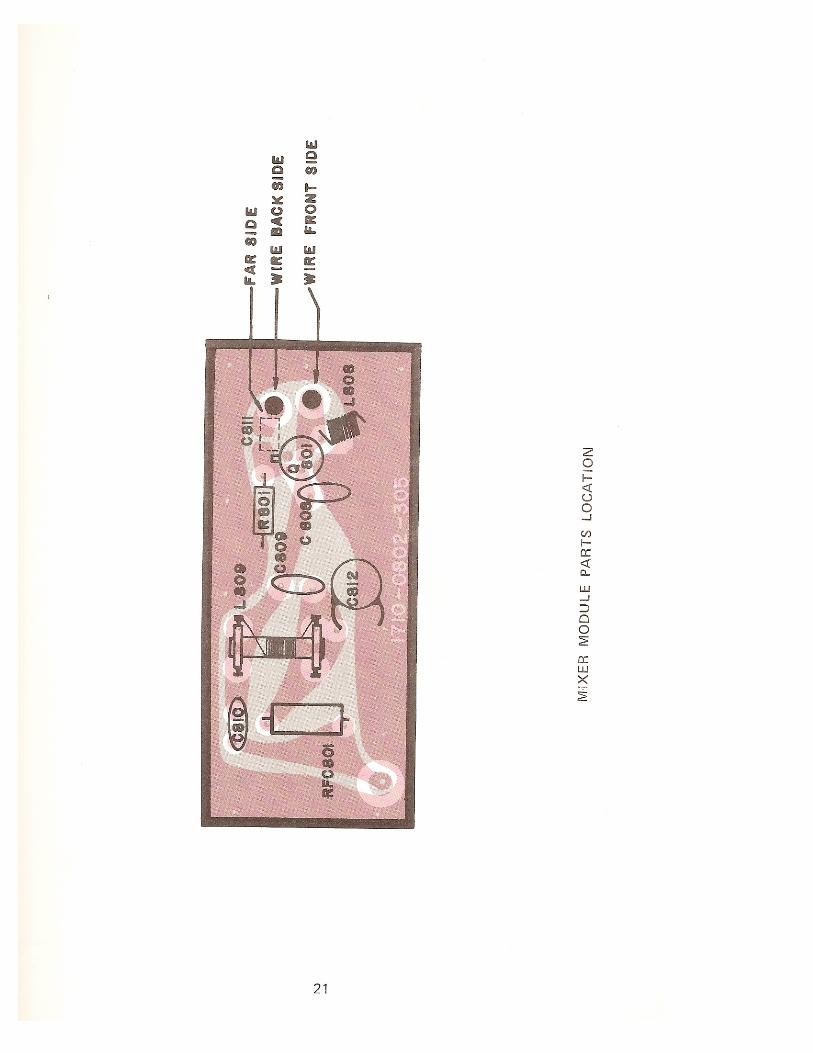
Mixer ................................................................................21 ...................................22
Receiver Multiplier ........................................................... 24 ...................................26
I.F .................................................................................... 28 ...................................27
Squelch ........................................................................... 30 ...................................32
Receiver Audio ................................................................ 34 ...................................33
Master Interconnect ......................................................... 36 ...................................38
Front Panel ..................................................................... .40 ...................................39
Rear Panel ..................................................................... .42
Options:
1091 Audio Amplifier ........................................................... .............. (Description) 43
10 W Receive Audio Board ................................... .44 ...................................46
1088 Preamp ....................................................................... .............. (Description) 47
R. F. Preamp Board .............................................. .48 ...................................50
Repeat Audio Interface ........................................................ ..............(Description) 51
Repeat Audio Interface Board ................................56 ...................................55
Carrier Operated Relay Board ................................ 58 ...................................60
Master Interconnect Schematic ............................................................................... 61
INSTRUCTION MANUAL
Section 1
GENERAL DESCRIPTION
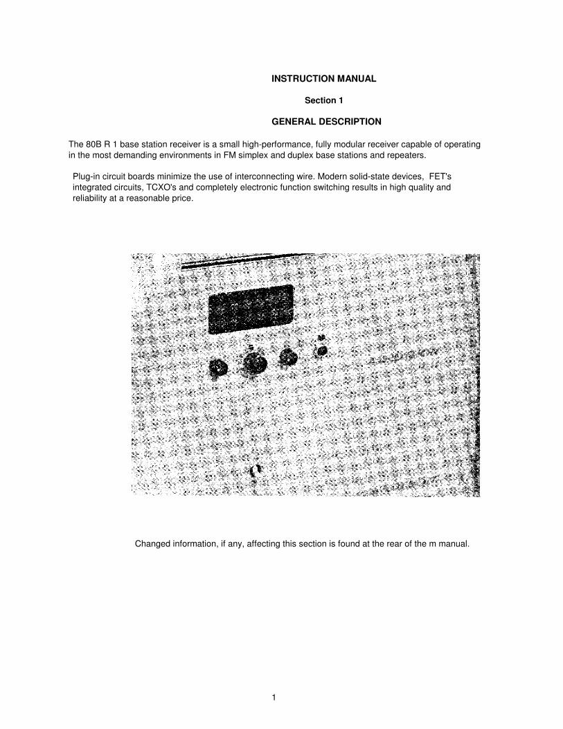
The 80B R 1 base station receiver is a small high-performance, fully modular receiver capable of operating
in the most demanding environments in FM simplex and duplex base stations and repeaters.
Plug-in circuit boards minimize the use of interconnecting wire. Modern solid-state devices, FET's
integrated circuits, TCXO's and completely electronic function switching results in high quality and
reliability at a reasonable price.
Changed information, if any, affecting this section is found at the rear of the m manual.
1

GUARANTEED MINIMUM PERFORMANCE
General Specifications
FCC Data Number .............................................80BR 1
Size. . . . . . . . . . . . . . . . . . . . . . . . . . . . .. 7"H x 19"W x 5"0
Weight ...............................................................6.5 Pounds
Power Requirements:
28 or 15.0 volts DC negative ground, receiver squelched, 250 mA
28 or 15.0 volts DC negative ground, receiver unsquelched, .8 amperes at 5 Watts audio output.
Sensitivity .......................................................... 0.35 microvolt, 12 dB SINAD
0.5 microvolt, 20 dB quieting
Adjacent Channel Rejection .............................. 90 dB
Modulation Acceptance ..................................... +7KHz
Squelch Sensitivity ............................................ 0.25 microvolt to 1.0 microvolt
Frequency Stability ............................................± .0005% from -30 C to +60 C
(±.00025% optional)
Multi-Frequency Spread .................................... 2.25 MHz
Number of Channels ..........................................Up to 4
Audio Power Output .......................................... 5 Watts (10 Watts at less than 5%
distortion optional)
Intermodulation ................................................. 80 dB
Spurious & Image Rejection ..............................100 dB
All Measurements per EIA RS-204A and RS·152B
2

Section 2
OPERATING INSTRUCTIONS
Controls:
All controls for normal operation are on the front panel. The on-off switch controls power to all circuits. Volume and squelch are rotary controls for ease of adjustment. Channel selection, when provided, is also affected by a rotary switch; Optional front panels without controls for remote controlled operation, or with additional microphone inputs or handsets, are available.
Operation:
To turn the unit on, switch power switch to the 'ON' position. Rotate the squelch control until speaker noise is obtained. Adjust the volume control for desired noise level. Now adjust the squelch control (no signal present) until the receiver is silenced.
3
2. ANTE"4"4A
.J::>. 1.
FL60D Q60D
10.7 MHZ Q601
CRYSTAL I -~ ~>----.B~~~:::S ~---------
80BRI
I
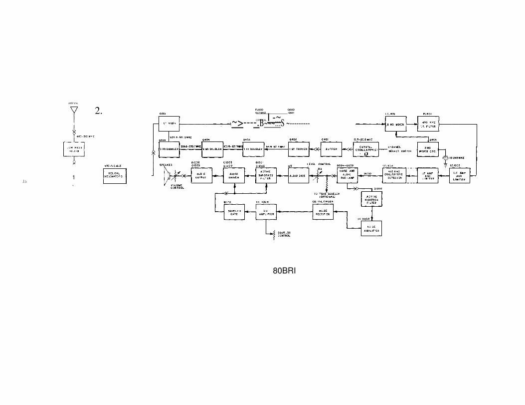
CIRCUIT DESCRIPTION
Receiver:
The receiver in this equipment is a dual-conversion superheterodyne design, which will receive on any
of four switch selected crystal controlled channels in the 406 to 512 MHz range.
The front end assembly consists of five highly selective resonators tuned to the receive frequency, a mixer
assembly which converts the desired frequency to 10.7 MHz, and two resonators tuned
to the local oscillator injection frequency (10.7 MHz below receive frequency of 450 + 512 MHz and 10.7
above for receive frequency of 406 to 450 MHz).
All entry and exit of signals and power from the front-end is made through coaxial cables.
The mixer is a junction FET in a common source configuration. Local oscillator signal is injected at the source while desired signals are coupled in the gate. The intermediate frequency of 10.7 MHz is selected by a resonant network in the drain circuit. The IF frequency is carried out and DC power for the mixer brought in by the same coaxial cable.
The receive TCXO (temperature compensated crystal oscillator) assemblies are added on a per channel
basis. Crystal frequencies in the 17 to 20 MHz range are used for basic frequency selection. Oscillator
outputs are connected to the input of a buffer for amplification and isolation from subsequent
amplifier/multipliers.
The buffered oscillator signal is multiplied twenty-four times by the receiver multiplier circuit. The
sequence of multiplication is 3 x 2 x 2 x 2. Each stage, except 0401 and 0405, is followed by double-
tuned circuits to eliminate undesired output products. The output of the multiplier assembly is coupled by
coaxial cable to the front end assembly where the 416.7 to 501.3 injection frequency is selected and
coupled to the mixer.
The mixer output is coupled to the I.F. at J601. The I.F. selectivity is established by an eightpole
monolithic crystal filter. I.F. noise figure is determined by filter insertion loss and a high gain, low noise
cascode input amplifier. The 10.7 MHz signal is mixed with a 10.245 MHz signal from a crystal-controlled
oscillator to produce a 455 kHz second I.F. frequency.
A three-pole miniature ceramic filter is employed to select the desired mixer product and to further
improve I.F. selectivity.
An integrated circuit differential amplifier follows the ceramic filter and provides approximately 25 dB of gain. The output of this stage is tuned and matched to the input of IC-603 where the majority of I.F. gain is obtained. IC-603 contains a quadrature detector which requires only one tuning adjustment for proper alignment.
5
The output of the quadrature detector is amplified by a broadband amplifier. The
output of th is am pi ifier is connected th rough a de-emphasis network to an emitter
follower and out to the level control. The output of the broadband amplifier is also
filtered for RF and coupled to an emitter and subsequently to the input of the squelch
circuit.
The squelch circuit consists of a bandpass filter, a detector, and a switch. The input
circuit is a high pass filter. This is followed by a low pass filter/amplifier. The detector
rectifies noise and the subsequent D.C. amplifier controls the squelch gate. The
reference level for squelch action is set with the squelch potentiometer.
The audio amplifier consists of an active bandpass filter and a direct coupled audio
amplifier using compound connected class AB output amplifiers. The input stage
serves as a high pass filter while 0302 is connected in an active lowpass amplifier
configu ration.
All receiver circu its except the direct coupled amplifier portion of the audio amplifier
are supplied by regulated 9.5 VDC from the regulator circuit. The receiver regulator
delivers output whenever the radio is "ON" .
. Frequency Control:
Frequency Control is obtained by using high stability crystals which maintain ±0.0005%
stability from a'to +600c. A negative temperature co-efficient thermistor located adjacent
to the channel crystal senses the crystal ambient temperature. At nominal ambient
temperature, (001:0 60<t) the resistance of thermistor is very low, placing a selected
fixed NPO capacitor essentially across the crystal to produce a nominally 32 pf load
capacitance. At low ambient temperatures (below OOC) at which high stability AT cut
crystals drop in resonant frequency, the resistance of this thermistor increases
exponentially. This causes a net reduction in the load capacitance across the crystal, so
that the oscillator frequency is held constant within ±.0005%. A high-stability air
dielectric capacitor is used for frequency adjustment, and the oscillator is powered from
a regulated 9.5V supply. Resistive isolation of the oscillator output as well as an
untuned buffer amplifier assure that load variations do not affect the transmitter
frequency. The oscillators are housed in a metal compartment to minimize radiation of
unwanted spurious signals as well as to provide an isothermal surface surrounding both
the crystal and thermistor.
Channel Selection:
The basic 80BR 1 is supplied with four channel capability, selected by applying +9.5
VDC to individual TCXO's from the front panel switch or rear panel terminal strip.
6

3. 4.
ALIGNMENT
A. Preliminary Voltage Adjustment:
(a) Connect a 15.0 volt power supply TB 1-5 or 28 volt power supply to TB 1-6.
(b) Turn the unit on and connect voltmeter to TP902 (white) (J4-14) on
the regulator board. Set R904 (9.5 adjust) for 9.5 volts.
(c) Connect the voltmeter to TP901 (red) (J4-13) on regulator board. Set
R912 for 13.8 volts.
B. Receiver Alignment Procedure:
1. Receiver Multiplier Alignment
(A) Connect VTVM to TP1 tune L401 for maximum reading (.6 - .8V). (TP1 is terminal "1" on connector J4).
(B) With VTVM connected to TP1 Tune L402 for a dip or minimum.
Tune L409 and L403 for a maximum.
(C) Connect VTVM to TP2. Tune L404 for a minimum. Tune L405 for a maximum.
(D) Connect VTVM to TP3. Adjust L402, L403, L409, L404, and L405 for a
maximum. Reading should be .4 volt or greater.
(E) Connect VTVM to TP4, Adjust L407 for a maximum indication.
Adjust alternately L406 and L407 for a maximum indication.
(F) Adjust C429 (VTVM still at TP4) for minimum indication on scale.
Reading should be .4 volts or more. 7

5. R.F. Front End Alignment
(A) Connect an on-frequency unmodulated signal to the antenna terminal. In-
crease signal level until receiver quieting is detected. If front end is badly
misaligned or tuned to a frequency 20MHz from the new frequency, signals
as great as 30 Mv. may be required for quieting. Tune C806 and C807
(injection frequency resonators) for best quieting.
(B) Tune C801 through C805 for best quieting. Continually reduce signal input level as alignment progresses. Each front end resonator should be repeaked twice or three times (in complete sequence) for proper alignment and optimum selectivity.
(C) Realign C806 and C807 for best quieting.
(D) If I.F. output circuit hasn't been aligned, refer to I.F. and passband align-
ment (this section) for correct procedure.
(E) Quieting sensitivity (20 dB) without pre-amp should be 0.5 uv. or better.
3. Receiver Oscillator Frequency Adjustment
Use one of the following procedures.
(A) With a 10.7 MHz signal source loosely coupled to the I.F., connect a generator
exactly on-frequency to the antenna input and adjust the receiver oscillator
trimmer for a zero beat at the audio output.
(B) Connect a frequency counter to P110 (17-21 MHz) on osc. carrier assembly and adjust the receiver oscillator trimmer for the correct crystal frequency.
(450 - 512 MHz) (406 - 450 MHz)
F crystal = F (receiver) -10.7 MHz F crystal = F receiver + 10.7 MHz
24 24
Receiver: 4. I.F. and Passband alignment
(A) Connect a 10.7 MHz signal generator through a capacitor to the input
(B) connector of the I. F. With a scope connected to TP-60 1, adjust the level of
10.7 MHz signal for presentation on the scope. Adjust L-600, L-601 and L-
602 for maximum indication.
(B) Connect scope to TP602. Reducing input to I.F. as necessary to prevent
limiting, adjust T600 and T601 for maximum indication.
(C) Disconnect 10.7 MHz generator and connect front-end output to I.F input. Connect signal generator capable of external FM modulation to
antenna connector. If front end is not properly aligned, perform that
procedure next.
8

(D) Connect oscilloscope probe to TP601. Adjust RF output level to 1000-3000 uv on
channel. Connect sweep output of oscilloscope (sawtooth) to Ext. Mod. input
terminals of signal generator. Adjust modulation level for at least + 8 KHz deviation
for full scope presentation and adjust scope sweep rate for approximately 5-10 mi
IIisec./division.
Observe passband on scope and adjust signal generator frequency and level and
scope sweep rate for best presentation (be sure waveform is not amplitude
limited). Adjust L-600 and L-601 for minimum ripple.
(E) Move oscilloscope probe to TP602. Reduce input signal level to 5-15 uv. Adjust
oscilloscope and generator level for best oscilloscope presentation. Tune T600 for
optimum flatness of the response trace. It may be necessary to remove the cover
from the front-end assembly and adjust L809. Adjust L600, L601 and L809
alternately for minimum ripple. It should be possible to reduce aggregate ripple
amplitude to less than 1.5 dB. The signal generator attenuator can be used to
measure the ripple amplitude in the following manner:
(1) Choose a point in the I. F. passband response presentation that has an adjacent
maximum and minimum response. Set the maximum response point at an
arbitrary position on the scope face. Make a mental note of the relative dB level
on the generator output until the minimum point is at the same
level as the previously established reference. Take this dB level indicated by
the attenuator and subtract it from the first reading. The difference is the
aggregate ripple amplitude and should be less than 1.5 dB.
Discriminator Alignment:
NOTE: Caution - Do not adjust L600 and L601. If adjustment of these coils becomes
necessary refer to passband alignment in the alignment instructions.
The I F amplifier uses a quadrature detector discriminator. This type does not have a DC
"zero" and cannot be used to net the receiver to a transmitter. Discriminator alignment is
limited to adjusting a single quadrature coil for maximum recovered audio with a normal input
signal, modulated 3-5 KHz at 1 KHz audio.
(a) Apply a modulated on-channel signal to the receiver.
(b) With the oscilloscope probe at J602 (top of the audio preset potentiometer) or AC
VOM/VTVM across the speaker terminals and the receiver unsquelched, peak L603
for a miximum output.
(c) Adjust R32 (audio level preset) for rated receiver audio output. Volume control on
front panel must be fully clockwise.
9

TROUBLESHOOTING
(Refer to schematics and parts list in the manual when performing maintenance on
the unit. Also, refer to circuit descriptions in Section 3. Transistor and integrated circuit pin layouts as well as color code information is given below.)
The radio is constructed with individual circuit "blocks" contained on separate modules or plugin printed
circuit boards. The major assemblies are shown opposite the schematic diagrams to aid in fault isolation
as well as normal preventive maintenance and alignment.
Most of the assemblies simply plug in, and fault isolation can often be simplified by substituting a known good module for the suspect assembly.
Because individual boards plug in, emergency repairs can usually be made by simply replacing the
defective board. The defective board can then be repaired at the serviceman's convenience.
BE SURE NOT TO TRANSPOSE WIRES WHEN SERVICING THE UNIT, SINCE SEVERE DAMAGE
TO CIRCUIT BOARD AND COMPONENTS MAY RESULT.
10
Troubleshooting Equipment:
The following equipment is helpful for troubleshooting the radio.
1. 1037 Test Set
2. Oscilloscope, to observe RX and TX audio and for sweep alignment.
3. Power supply adjustable from 14.0 to 16.0 VDC or 24 to 28 VDC at 2 amp load.
4. Signal Generator, 406-512 MHz, 0.1 microvolt to 200 millivolt output, internal 1 kHz
modulation. (Measurements Model 800 or equivalent)
5. Frequency Counter with time base stability of ± .0001% or better.
6. 10.7 M Hz signal source (in Iieu of the 1037 test set)
7. VOM or VTVM with low DC voltage range and 20K ohm/V or higher input impedance
(SIMPSON 260 or equivalent) (in lieu of 1037 Test Set)
A number of companies manufacture combined test equipment that may be used for most ad-justments and troubleshooting.
When circuit malfunctions exist, a visual check of the unit may reveal the portion of the unit in
which the trouble is located. Check for broken or disconnected wires, damaged circuit boards,
damaged components, etc.
To isolate trouble to a circuit, note the symptom. For example, failure of the squelch to function at any setting of the squelch indicates that the squelch board is probably at fault. However, failure of the squelch to open with a signal, although it will open when the squelch control is rotated, indicates that oscillator, front end, IF, or squelch board problems may exist.
In this case a more complete determination must be made by signal tracing and/or voltage
measurements.
In any signal tracing analysis, a good oscilloscope is indispensable. Care should be exercised, of course, to avoid misinterpretation of readings which appear to indicate malfunctions in tuned circuits. A scope can severely detune a critical circuit so that any readings taken are rendered meaningless. This is minimized with a compensated 10X probe, but not entirely eliminated.
11

TROUBLESHOOTING CHART
The following chart may be helpful, in conjunction with schematic, voltage charts, and circuit de-scription, for all troubleshooting work.
PROBLEM
1. Receiver dead, audio and squelch
function with front panel controls
2 Receiver audio dead
3. Squelch malfunction
4. Receiver signal distorted
5. Poor receiver sensitivity
6. Fuse blows when power is connected
CHECK CIRCUIT BLOCK
Oscillators, mixer board, Rec. multiplier,
IF
Receiver audio board, squelch board, voltage
regulator,
Squelch board, oscillators, IF, front end, voltage regulator,
Audio amp, receiver oscillators, IF, voltage
regulator, level control
Mixer board, I F board, receiver audio, re-
ceiver multiplier.
Regulator circuit, Rec. audio amp, master
interconnect, wiring, cables.
12
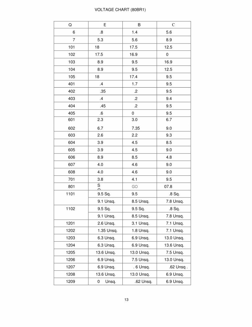
VOLTAGE CHART (80BR1)
Q E B C
6 .8 1.4 5.6
7 5.3 5.6 8.9
101 18 17.5 12.5
102 17.5 16.9 0
103 8.9 9.5 16.9
104 8.9 9.5 12.5
105 18 17.4 9.5
401 .4 1.7 9.5
402 .35 .2 9.5
403 .4 .2 9.4
404 .45 .2 9.5
405 .6 0 9.5
601 2.3 3.0 6.7 ,
602 6.7 7.35 9.0
603 2.6 2.2 9.3
604 3.9 4.5 8.5
605 3.9 4.5 9.0
606 8.9 8.5 4.8
607 4.0 4.6 9.0
608 4.0 4.6 9.0
701 3.8 4.1 9.5
801 SO
GO 07.8
1101 9.5 Sq. 9.5 .8 Sq.
9.1 Unsq. 8.5 Unsq. 7.8 Unsq.
1102 9.5 Sq. 9.5 Sq. .8 Sq.
9.1 Unsq. 8.5 Unsq. 7.8 Unsq.
1201 2.6 Unsq. 3.1 Unsq. 7.1 Unsq.
1202 1.35 Unsq. 1.8 Unsq. 7.1 Unsq.
1203 6.3 Unsq. 6.9 Unsq. 13.0 Unsq.
1204 6.3 Unsq. 6.9 Unsq. 13.6 Unsq.
1205 13.6 Unsq. 13.0 Unsq. 7.5 Unsq.
1206 6.9 Unsq. 7.5 Unsq. 13.0 Unsq.
1207 6.9 Unsq. . 6 Unsq. .62 Unsq .
1208 13.6 Unsq. 13.0 Unsq. 6.9 Unsq.
1209 0 Unsq. .62 Unsq. 6.9 Unsq.
13


PARTS LIST
Item Description Part No
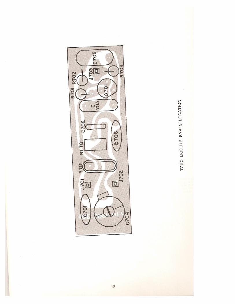
TCXOBOARO
Component parts selected at manufacture to comply with
FCC stability requirements. To order complete assembly,
state part number and channel frequency.
Receive: 1939-0802-134
20


![SERVICE AND OPERATION MANOO AND OPERATION MANOO. MTG-XX01 SERIES [13",19"] ... it is recommended to use only high quality Happ Controls replacement ... C807 ; C ELECTRO . 16V 1OOuF](https://static.fdocuments.in/doc/165x107/5b1913eb7f8b9a1e258c7869/service-and-operation-and-operation-manoo-mtg-xx01-series-1319-it-is-recommended.jpg)