TABLE OF CONTENTS - resources.altium.com · Disable "Mark Manual Parameters": If enabled, manually...
40
Transcript of TABLE OF CONTENTS - resources.altium.com · Disable "Mark Manual Parameters": If enabled, manually...


TABLE OF CONTENTS
MIGRATING FROM ORCAD TO ALTIUM DESIGNER
www.altium.com
The Altium Designer Philosophy 2
Preparing Your OrCAD® and Allegro® Files 3Importer InstallationSupported OrCAD® Versions & File FormatsASCII File Creation
Translating Your Schematics 6Schematic Import ProcessSchematic Cleanup
Translating Your PCBs 16 PCB Import ProcessPCB Design Cleanup
Translating Your Schematic Symbol Libraries 26Schematic Symbol Library Import ProcessSchematic Symbol Library Cleanup
Synchronizing Your Schematics and PCBs 32Project ManagementSynchronizationEngineering Change Orders
Your Next Steps in Altium Designer 39

MIGRATING FROM ORCAD TO ALTIUM DESIGNER
www.altium.com
The core principle of Altium Designer is a unifi ed approach to PCB design. In implementing this approach, you’ll fi nd that our tool diff ers from many of the more conventional alternatives cur-rently available. There are a number of separate yet connected elements required to complete a successful PCB design, and our workfl ow brings them all together.
As an existing OrCAD® or Allegro® user, you’re likely used to having multiple tools and interfaces for each stage of your design process. And while each tool excels in its own specialized task, at the end of the day you’re left to manage and remember multiple interfaces, workfl ows, and me-thodologies. Throughout our tenure in PCB design, the question we’ve always asked is this: Is that approach really eff ective?
When we fi rst created Altium Designer, we wanted to create an experience that kept the engineer in complete control of their effi ciency and workfl ow throughout the entire design process. Achie-ving this goal meant getting to the heart of the matter: what, exactly, does a complete PCB design experience entail for the everyday engineer? As part of our approach, we connected the following processes into a single interface:
• Schematic Capture• Board Layout• Design Data Management• Rules and Constraints• Bill of Materials• Supply Chain Integration• Engineering Change Management• MCAD Collaboration• Manufacturing Documentation
With all of these elements integrated into a single, all-encompassing interface, switching back and forth between tasks becomes as simple as selecting the appropriate fi le to work on in your design workspace. The interface then handles all the rest and provides the tools you need for the parti-cular task at hand.
Our unifi ed PCB design approach has continued to grow and evolve over 30 years of research and development. We’ve found it to be, quite simply, the most effi cient way to design electronics. This philosophy extends not just to the individual engineer, but also to the entire design team. Multiple engineers can all work on diff erent aspects of the same project using the same interface, and no time is wasted translating design data back and forth between design environments.
We hope you enjoy your journey into the world of Altium Designer.
Mike Moore, Field Applications Engineer & The Altium Designer Team
The Altium Designer Philosophy
2

MIGRATING FROM ORCAD TO ALTIUM DESIGNER
www.altium.com
Import Wizard InstallationBefore beginning any OrCAD® fi le preparation, the fi rst step is to make sure both the OrCAD® and Allegro® Importers have been installed. This can be done directly within Altium Designer, using the following steps:
1. Open Altium Designer2. Select File » Import Wizard3. Select Next on the Welcome screen
The next screen, 'Select Type of Files to Import', lists the installed importers.
Preparing Your OrCAD® and Allegro® Files
During the Altium Designer installation process, you can choose which Importers and Exporters to install. Neither the OrCAD® nor Allegro® translators are part of the default installation, and must be selected manually.
If either the 'Allegro Design Files' or the 'OrCAD Design and Libraries Files' entries are missing from the list as shown above, then follow these steps to add them:
1. Select Get More Importers at the bottom-left corner of the Import Wizard dialog window. This will open the Extensions & Updates tab inside the Altium Designer environment.
Altium Designer Import Wizard fi le type selection
3

MIGRATING FROM ORCAD TO ALTIUM DESIGNER
www.altium.com
4. Scroll back to the top and select 'Apply'. You will then need to restart Altium Designer to complete the installation.
5. Select File » Import Wizard and confi rm that the Allegro® and OrCAD® Importers have been added.
With the importer added in Altium Designer, you are now ready to start preparing your OrCAD® and Allegro® fi les for the import process.
Preparing Your OrCAD® and Allegro® Files
2. Select 'Confi gure' on the right and scroll down to the Importers\Exporters section.3. Check the boxes next to Allegro® and OrCAD® to enable the extensions.
Altium Designer Extensions & Updates section
Enable the Allegro® and the OrCAD® importers in the Altium Designer Extensions & Updates section
4

MIGRATING FROM ORCAD TO ALTIUM DESIGNER
www.altium.com
Preparing Your OrCAD® and Allegro® Files
Supported OrCAD® Versions & File FormatsThe OrCAD® Import Wizard for Altium Designer supports a variety of file versions, listed below. It is recommended to use the latest OrCAD® file version(s) available.
• OrCAD® Capture - V16.x, V15.x, V10.x, V9.x• OrCAD® PCB Editor (Allegro) - V16.x, V15.x, V14.x• OrCAD® Component Information System (CIS)
NOTE: OrCAD® Layout V9.x is also supported in the OrCAD® Designs and Libraries Files Importer. However, that product was End-of-Lifed in 2009, so we won’t go into it here.
Please keep the following things in mind when using the Import Wizard:
• The Import Wizard will translate schematics, PCBs, and CIS configuration library files.• OrCAD® Layout has been discontinued and replaced with OrCAD® PCB Editor (Allegro®)• The source OrCAD® PCB Editor binary files (e.g. ‚*.brd’ for board files) are the same
as Allegro®.• The Import Wizard handles both OrCAD® PCB Editor/Allegro® Design files (.brd) and
OrCAD® PCB Editor/Allegro ASCII Extract files (.alg). If you have OrCAD® PCB Editor/Alle-gro versions 15.2 or 16.x installed, you can directly translate OrCAD® PCB Editor/Allegro Design files (.brd) into Altium Designer PCB files (.PcbDoc) Note: A free OrCAD® demo or OrCAD® PCB Designer Lite copy is sufficient.
• The CIS portion of OrCAD® Capture CIS will not be covered here. However, if you want to translate OrCAD® Capture CIS to Altium Designer, you can find instructions here: Translating CIS to Altium Designer
5

MIGRATING FROM ORCAD TO ALTIUM DESIGNER
www.altium.com
Translating Your Schematics
OrCAD® Capture .DSN schematic fi les to Altium Designer
1. Select File (top left) » Import Wizard.
6
2. The Import Wizard dialog box will appear. Click 'Next' to proceed.

MIGRATING FROM ORCAD TO ALTIUM DESIGNER
www.altium.com
Translating Your Schematics
7
3. Select OrCAD® Designs and Libraries Files in the Select Types of Files screen. Click 'Next'.
4. Click 'Add' to browse to the location of the .DSN fi le you wish to import. The fi le will appe-ar as shown in the fi gure below. Click 'Next' to continue.

MIGRATING FROM ORCAD TO ALTIUM DESIGNER
www.altium.com
Translating Your Schematics
8
5. To add OrCAD® OLB libraries, click the 'Add' button to select the library fi le(s) you wish to import. Click 'Next' to continue.
6. The Reporting Options page will enable/disable the settings for logging errors, warnings, and events respectively. Click 'Next' to continue.

MIGRATING FROM ORCAD TO ALTIUM DESIGNER
www.altium.com
Translating Your Schematics
9
7. It is recommended to keep this box selected, as shown below, so that rectangles areimported properly. Click 'Next' to continue.
8. Use the following Title Block and Pin-to-Pin Spacing options to control how OrCAD®
schematic pages are imported. Click 'Next' to continue.

MIGRATING FROM ORCAD TO ALTIUM DESIGNER
www.altium.com
Translating Your Schematics
10
9. The Schematic Parameter and Net Connectivity Options dialog box controls the way Parameters and Junctions are handled. The defaults are shown below. Click 'Next' to continue.
Auto-position parameters: This option will override the imported component parameter locations and use the justifi cation settings of the parameter for positioning.
Disable "Mark Manual Parameters": If enabled, manually positioned component para-meter locations are marked with a visual indicator. This preference can be re-enabled in Altium Designer by going to DXP » Preferences » Schematic » Graphical Editing » Mark Manual Parameters.
Import OrCAD Junctions: When set to All, a manual junction will be added to both 3-way and 4-way wire junctions. When set to Only Cross Junctions, manual junctions will only be added to 4-way wire junctions. All other junctions will be generated automatically.

MIGRATING FROM ORCAD TO ALTIUM DESIGNER
www.altium.com
Translating Your Schematics
11
10. The default project location for the import process is shown below. Click 'Next' to continue.
11. The Messages panel may appear, which provides an interactive listing of the error, warning and status messages produced during the import. This dialog box can be closed by clicking the 'x' in the top right corner of the dialog box.

MIGRATING FROM ORCAD TO ALTIUM DESIGNER
www.altium.com
Translating Your Schematics
12
12. If the translation process is successful, then the Wizard is complete. You can click to close it and start working on your translated Schematic designs in Altium Designer. Click 'Finish' to complete the import process.
Schematic CleanupThere will always be at least a little bit of cleanup work to do. This is usually due either to incompa-tibilities between the two CAD systems’ data structures, or just diff erences in how certain features or object types were implemented.
In this section, we’ll address the common areas of the translated schematic that should be inspec-ted. For this and subsequent cleanup sections, the assumption is that the user has at least a basic understanding of Altium Designer and how it’s used. To learn the basics of Altium Designer, please view the Getting Started with Altium Design documentation.
For further information on editing multiple objects, please refer to the following link:http://techdocs.altium.com/display/ADOH/Editing+Multiple+Objects

MIGRATING FROM ORCAD TO ALTIUM DESIGNER
www.altium.com
Translating Your Schematics
13
Manually Placed ParametersVisible component parameters in Altium Designer are usually set as autopositioned. This means that the system will place the parameter - including a reference designator - in a default location alongside the symbol body. This is helpful when rotating components, as the system will place the parameters in a neat and readable position.
In an eff ort to duplicate the source schematic exactly from OrCAD® Capture, imported parame-ters have their autoposition setting disabled. The reference designators and parameters are then placed as close to their original position as possible, and are now considered manual parameters.
Because of diff erences in default text styles and sizes, an exact match may not always be possible. The user may want to make slight changes to the parameter text positioning.
Parameters that are manually positioned are marked with a small dot as shown below:
Manually positioned parameters on a schematic symbol

MIGRATING FROM ORCAD TO ALTIUM DESIGNER
www.altium.com
Translating Your Schematics
14
You can choose to handle these manual parameters in one of three ways:
1. Leave the design as-is.2. Leave the parameters where they are but turn off the dot. This can be done by going to
Tools » Schematic Preferences, then selecting the Graphical Editing group and disabling the "Mark Manual Parameters" option.
3. Re-enable the Autoposition setting in the Parameter Properties dialog as shown below. This can be done by using a combination of Find Similar Objects and the SCH Inspector panel.
Because the autopositioning of parameters is only done during either component placement or the rotation process, the eff ect of the autoposition won’t be seen until the components are rotated in place.
A quick way to rotate all components in place:
1. Press Ctrl+A to select everything on the schematic sheet2. Press Spacebar to rotate everything 90 degrees3. Press Shift+Spacebar to rotate everything back to their original positions
All parameters and designators will now be positioned automatically.
Editing Parameter Properties in Altium Designer

MIGRATING FROM ORCAD TO ALTIUM DESIGNER
www.altium.com
Translating Your Schematics
15
Connectivity DifferencesIn OrCAD® Capture, net connectivity is made using net aliases, off-page connectors, hierarchical blocks and hierarchical ports, and globals. Nets between schematic pages within a single sche-matic folder are connected through the off-page connectors, while the hierarchical blocks and ports connect the nets between the schematic folders. Globals are used to connect power/gnd nets throughout the design. Altium Designer uses a similar set of net identifiers to create net connectivity. Within a schematic sheet you can use wires and netlabels. Between schematic sheets, nets in a flat design are typically connected using ports, but off-sheet connectors are also available. Off-sheet connectors are purely graphical and do not contain any electrical characteristics. For this reason, it’s recommended that you use ports. Nets in a hierarchical design are connected from a port on the lower sheet to a sheet entry of the same name, in the sheet symbol that represents the lower sheet. Power/ground nets are connected using power ports.
Connectivity problems may become evident after running the project compile process (Project » Compile PCB Project). The Messages panel will report all errors and warnings that indicate hier-archical and net connectivity mismatches. For instance, a Duplicate NetNames error usually points to improper sheet-to-sheet connectivity.
Rather than address every possible situation here, we recommend that you familiarize yourself with Connectivity and Multi-Sheet Design within the TechDocs.

MIGRATING FROM ORCAD TO ALTIUM DESIGNER
www.altium.com16
OrCAD® PCB Editor (Allegro) to Altium DesignerThe translation of OrCAD® PCB Editor (Allegro) Design files can be handled by the Altium Designer Import Wizard. Complete flexibility is found in all pages of the wizard, giving you as little or as much control as you would like over the translation settings before you commit to the actual trans-lation process.
The Import Wizard handles both Allegro PCB Design files (*.brd) and Allegro ASCII Extract files (*.alg). If you have Allegro PCB Editor version 15.2 or 16.x installed, you can directly translate Alle-gro PCB Design files (*.brd) into Altium Designer PCB files (*.PcbDoc).
Allegro ASCII Extract files (*.alg) can be created by running a batch process on an Allegro machine, as we’ll discuss later in the section „USING ASCII CONVERSION TO IMPORT WITHOUT ALLEGRO.” The ASCII files can then be translated, on machines without Cadence Allegro PCB Editor installed, to Altium Designer PCB files (*.PcbDoc). The benefit of this, is that you only need one licensed copy of Cadence Allegro PCB Editor to convert all of your designs into Allegro ASCII Extract files (*.alg), which can then be distributed to other team members for translation.
OrCAD® PCB Editor (Allegro) to Altium DesignerThe Import Wizard can be launched from Altium Designer‘s File menu. Choose Allegro Design Files from the list of File Types.
Files in the Import Wizard translate as follows:
• Allegro Binary PCB Design files (*.brd) translate to Altium Designer PCB files (*.PcbDoc).• Allegro ASCII Extract Files (*.alg) translate to Altium Designer PCB files (*.PcbDoc).
Alternatively, drag your Allegro Design Files into the Projects Panel which will automatically launch the wizard in Allegro Import mode.
Translating Your PCBs

MIGRATING FROM ORCAD TO ALTIUM DESIGNER
www.altium.com
Translating Your PCBs
17
1. Select the File » Import Wizard.
2. The following dialog box will appear. Click 'Next' to proceed.

MIGRATING FROM ORCAD TO ALTIUM DESIGNER
www.altium.com
Translating Your PCBs
18
3. Select the fi le type you wish to import (Allegro Design Files). Click 'Next'.
4. Click the 'Add' button to browse to the location of the .BRD (Binary) or .ALG (ASCII) fi le you wish to import. The fi le will appear as shown in the fi gure below. Click 'Next' to continue.
Note: If you to attempt to add OrCAD® PCB Editor (Allegro®) Design Files (*.BRD) to the Import Wizard, without a working copy of Allegro® on your machine, a warning will be displayed. Also note: You may still get the error message even if you have OrCAD® PCB Editor installed.

MIGRATING FROM ORCAD TO ALTIUM DESIGNER
www.altium.com19
Translating Your PCBs
If you encounter the "Dxp" dialog box below, please refer to the section entitled: "Using ASCII Conversion to Import Without Allegro" below. In that section, we’ll show you how to convert your binary board fi les into ASCII to import them into Altium Designer.
6. Use the Reporting Options page to enable or disable the settings for logging errors, warnings, and events respectively. Click 'Next' to continue.
A Log Report in ASCII fi le format (*.LOG) is generated for each translated Allegro® PCB fi le. This log is saved in the \Imported sub folder of your original Allegro® fi les. Open the Log Report after translation in a text editor to examine the details.
7. Specify Polygon Connect and Plane Connect Options for the PCB import process. Enable the Import Auto-Generated Copper Pour Cutouts option to import the voids that are automatically generated as cutouts in Allegro® PCB Editor when the fi le is translated.

MIGRATING FROM ORCAD TO ALTIUM DESIGNER
www.altium.com20
Translating Your PCBs
NOTE: It is highly recommended that you UNCHECK the Import Auto-GeneratedCopper Pour Cutouts option if you’re planning any edits to the board in Altium Designer. The default options are displayed below with the recommended change shown.
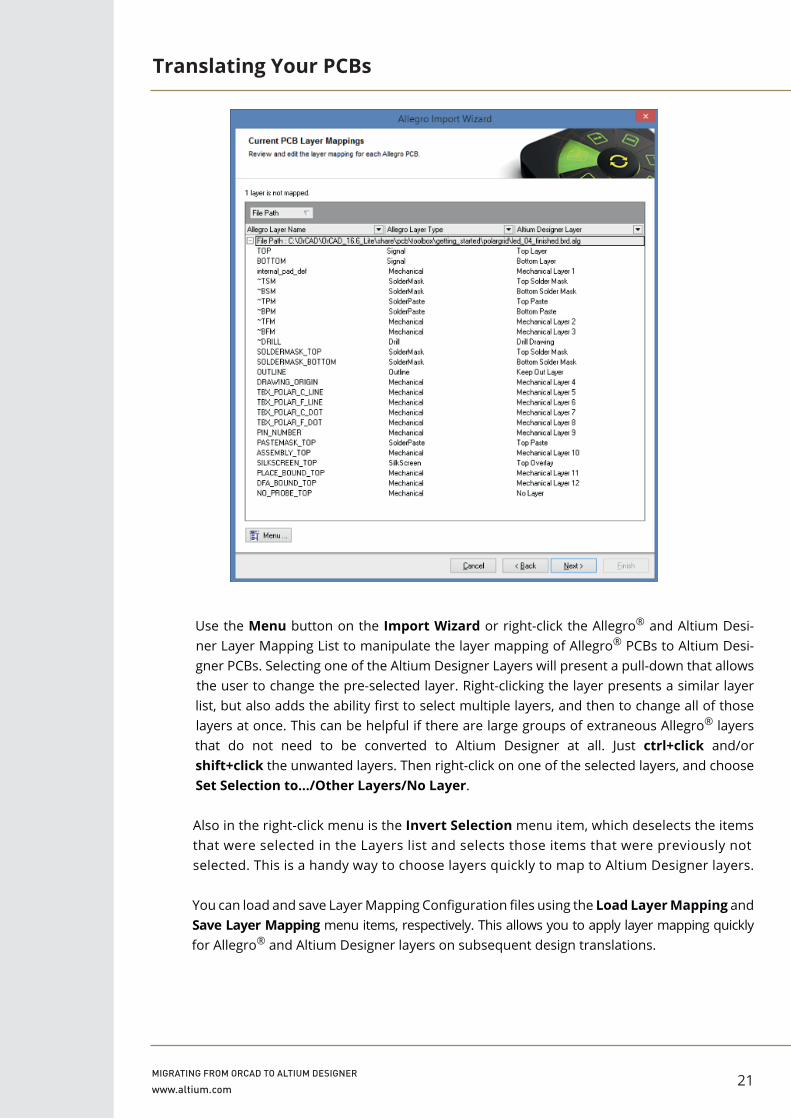
8. All used Allegro® PCB layers must be mapped to an Altium Designer layer prior to import. Layer Mapping is a mapping between the names of the Allegro® PCB layers and Altium Designer PCB layers.
Default mapping is provided by the Import Wizard to build the layer mapping for each PCB. Layer mapping can be customized for each of your designs to be imported. You may wish to import multiple Allegro® PCB designs and map the same Allegro® layer to the same Altium Designer layer. You can set your layer mapping once and use this layer map- ping for all of your fi les to be imported.
The advantage of this type of batch layer management is that it can save time when importing multiple designs. The disadvantage is that Default Layer Mapping is not always intelligent when it comes to diff ering structures in designs, so some manual changes may be required.
MIGRATING FROM ORCAD TO ALTIUM DESIGNER
www.altium.com21
Translating Your PCBs
Use the Menu button on the Import Wizard or right-click the Allegro® and Altium Desi- ner Layer Mapping List to manipulate the layer mapping of Allegro® PCBs to Altium Desi- gner PCBs. Selecting one of the Altium Designer Layers will present a pull-down that allows the user to change the pre-selected layer. Right-clicking the layer presents a similar layer list, but also adds the ability fi rst to select multiple layers, and then to change all of those layers at once. This can be helpful if there are large groups of extraneous Allegro® layers that do not need to be converted to Altium Designer at all. Just ctrl+click and/or shift+click the unwanted layers. Then right-click on one of the selected layers, and choose Set Selection to.../Other Layers/No Layer.
Also in the right-click menu is the Invert Selection menu item, which deselects the items that were selected in the Layers list and selects those items that were previously not selected. This is a handy way to choose layers quickly to map to Altium Designer layers.
You can load and save Layer Mapping Confi guration fi les using the Load Layer Mapping and Save Layer Mapping menu items, respectively. This allows you to apply layer mapping quickly for Allegro® and Altium Designer layers on subsequent design translations.

MIGRATING FROM ORCAD TO ALTIUM DESIGNER
www.altium.com22
Translating Your PCBs
9. The default project location for the import process is shown below. You can change the location if you wish. Click 'Next' to continue.
Each of the imported Allegro® Design Files is located in a separate subdirectory in a spe- cifi ed Project Output Directory. You can further customize the PCB projects by dragging Allegro® Design fi lenames to other Projects in the PCB Projects list.
10. The Output PCB Projects page is where each Allegro® PCB is converted to an Altium Designer PCB document (*.PcbDoc) in a design project. A number of intensive tasks, such as loading geometry data, translating nets and components, and generating vias and copper pour polygons, can make the process a bit time-consuming. You can monitor the status bar at the bottom of the Altium Designer workspace to see which operation is taking place at any given time. Please wait until the 'Cancel', 'Back', 'Next' and 'Finish' buttons are enabled to indicate that the processing is complete.

MIGRATING FROM ORCAD TO ALTIUM DESIGNER
www.altium.com
Translating Your PCBs
23
Using ASCII Conversion to Import Without Allegro®
An Altium Designer workstation that does not have a licensed Allegro® installation is still able to import Allegro® ASCII Extract fi les (*.alg). The following procedure enables a Licensed Allegro® user to convert Allegro® binary *.brd fi les to Altium compatible *.alg fi les. The conversion must be run on the Allegro-licensed machine.
1. Locate the following fi les in the \System folder of your Altium Designer installation:1.1 Allegro2Altium.bat1.2 AllegroExportViews.txt
2. Copy the two fi les to the folder containing the *.brd binary Allegro® version 15.2 or16.x fi le.
3. Open a command (DOS) prompt, navigate to the folder containing these fi les, andtype the following: Allegro2Altium your_fi le.brd
4. Surround your fi lename with double quotes if the fi lename contains spaces,i.e.: Allegro2Altium "your fi le.brd"
5. The ASCII fi le is now created in the folder. Copy the *.alg fi le to the Altium Designerworkstation and import using the Import Wizard.
Read on to fi nd out more about Altium Designer and your PCB designs.
11. If the translation process is successful, then the Wizard is completed. You can click to close it and start working on your translated PCB design in Altium Designer. Cleanup will be performed on the translated document fi rst before you can perform edits on it. Click 'Finish' to complete the import process.

MIGRATING FROM ORCAD TO ALTIUM DESIGNER
www.altium.com
Translating Your PCBs
24
PCB Design Cleanup
Although the translator does an excellent job of accurately converting the PCB data, incompati-bilities between the two CAD systems could result in the need for further editing to the imported design.
Design RulesWhen it comes to rule setup, Allegro® and Altium Designer are vastly different. Allegro® uses a separate constraint manager and Altium uses a matrix-based methodology. Design Rules set in Allegro® are not currently transferred to Altium Designer. These rules will need to be added ma-nually in Altium Designer.
KeepoutsKeepout objects have different capabilities in Allegro® than in Altium Designer. In Altium Designer, a keepout can be constrained to a specific layer and can have any physical shape, but it will apply the keepout to all electrical types, be it a via, trace, component pad, etc. By contrast, an Allegro® keepout can be configured to exclude specific object types (e.g., to keep out vias but not traces).
When an Allegro® keepout is configured to keep out more than one object type, only one keepout object will be created in Altium Designer. The type created will depend on which keepout options are set in Allegro® and how the Import Wizard Keepout options are enabled.
The keepout incompatibilities can also extend into PCB footprints. OrCAD® PCB Editor footprints can contain the same configurable keepout objects. It is common for designers to include, for example, a keepout area between the pads of an SMD capacitor, which prevents vias from being placed between the pads while still allowing traces.
In the footprint in Altium Designer, you may have a keepout region between the pads. In addition to the keepout checking for vias, it will also flag errors for any electrical item (traces, copper pours, etc.). In this situation, the Allegro® keepout may translate into an object that could produce unex-pected DRC violations.
If this situation occurs, then these footprints will have to be edited in the Altium library to remove the keepout.

MIGRATING FROM ORCAD TO ALTIUM DESIGNER
www.altium.com25
Translating Your PCBs
Polygon (Copper) Pour ThermalsAll PCB systems handle copper pour and thermal generation diff erently. Because thermal connects are, by defi nition, a design rule in Allegro®, this does not apply. We do not create design rules du-ring the import process to Altium Designer. The only option you have during the import process is to set a global setting in the fi gure below.
Altium Designer takes an altogether diff erent approach to thermal generation, by managing these settings in the design rules (Polygon Connect Style rules). In practice, this methodology allows for more effi cient thermal setup, due to the fact that all of the settings concerning thermal connec-tions are in one place.
The Altium Designer SMT connection rule will have its thermal spoke width determined by the 'SMT Thermals' spoke width setting in the PADS® Options » Thermals dialog. If any other specifi c thermal connection confi guration is needed, you will need to create these rules manually within Altium Designer. One common example is a rule that specifi cally targets vias for "fl ood over" connectivity. This is achieved by creating a new rule, and setting the Scope to "IsVia" vs."All" and the Constraints to "Direct Connect".
For more information on design rule creation, please refer to Creating Design Rules within TechDocs.
Confi guring design rules in Altium Designer for polygon connectivity

MIGRATING FROM ORCAD TO ALTIUM DESIGNER
www.altium.com
Translating Your Schematic Symbol Libraries
OrCAD® Schematic Symbol LibraryTo translate an OrCAD® schematic symbol library, you can simply import the .OLB fi le, by doing the following:
1. Select the File menu at the top of the screen, then select Import Wizard fromthe File menu.
26

MIGRATING FROM ORCAD TO ALTIUM DESIGNER
www.altium.com
2. The following dialog box will appear. Click 'Next' to proceed.
Translating Your Schematic Symbol Libraries
27
3. Select the fi le type you wish to import (OrCAD Designs and Libraries Files). Click 'Next'.

MIGRATING FROM ORCAD TO ALTIUM DESIGNER
www.altium.com
Translating Your Schematic Symbol Libraries
28
4. Click the 'Next' button to skip adding OrCAD® Designs Files. You can translate Design Files at the same time as Library Files (see above for details).
5. Click the 'Add' button to select the OrCAD® Library File(s) you wish to import.Click 'Next' to continue.
6. Below you see the default Schematic General Options. Select the applicable options.Click 'Next' to continue.

MIGRATING FROM ORCAD TO ALTIUM DESIGNER
www.altium.com29
7. Use the Reporting Options page to enable or disable the settings for logging errors,warnings, and events respectively. Click 'Next' to continue.
Translating Your Schematic Symbol Libraries
8. The Default Output Library Options are shown below. Change these options as desired. Click 'Next' to continue.

MIGRATING FROM ORCAD TO ALTIUM DESIGNER
www.altium.com30
Translating Your Schematic Symbol Libraries
9. The default project location for the import process is shown below. You can change the location if you wish. Click 'Next' to continue.
10. If the translation process is successful, then the Wizard is completed. You can click to close it and start working on your translated Capture Libraries in Altium Designer.Click 'Finish' to complete the import process.

MIGRATING FROM ORCAD TO ALTIUM DESIGNER
www.altium.com
Translating Your Schematic Symbol Libraries
31
When the process is complete, the translated schematic library can then be opened from the Projects panel
Schematic Symbol Library CleanupMost aspects of the schematic symbols translate accurately, including symbol graphics, pinnames and numbers, parameters, and pointers to footprints. However, some minor symbol library editing may be necessary.
OrCAD PCB Editor (Allegro)® PCB Footprint LibraryCurrently, our translator does not support importing any Allegro® PCB Footprint libraries. However, you can translate board fi les and then create libraries from those fi les in Altium Designer. You could also place a number of PCB Footprints from your Allegro libraries on a board and then translate them using the translator. You can then save the translated board as a library in Altium Designer.
Projects Panel in Altium Designer

MIGRATING FROM ORCAD TO ALTIUM DESIGNER
www.altium.com32
Synchronizing Your Schematics and PCBs
Project ManagementAlthough schematic and PCB designs can be translated during the same Import Wizard session, the translations are run as separate processes. When each design is translated, the resulting fi les will be placed into separate projects. In this example, the “Preview” schematic and “Previewpour” PCB design were run through the Import Wizard at the same time, but two separate projects and project folder structures were created.
Working with two separate projects imported into Altium Designer
If it is necessary to recreate the project fully, then some fi le management will need to be done. It is generally recommended that all project fi les reside in the same folder. Since there are usually multiple schematic documents and only one PCB document, the simplest thing to do is copy or move the ‘.PcbDoc’ fi le into the project folder where the ‘.SchDoc’(s) reside.
At this point, the imported PCB project is not needed (“previewpour.PrjPcb” in this example) so it can be closed. Right click the project name in the panel (“previewpour.PrjPcb”) and click Close Project. “Preview.PrjPcb” is now the working project from this point forward. The ‘.PcbDoc’ fi le now needs to be added to the project. Go to Project » Add Existing to Project, add the ‘.PcbDoc’ fi le, and then save the Project.
For more information on projects refer to Project Management within TechDocs.

MIGRATING FROM ORCAD TO ALTIUM DESIGNER
www.altium.com33
Synchronizing Your Schematics and PCBs
SynchronizationInstead of using Reference Designators to synchronize the schematic and the PCB, Altium De-signer uses a Unique ID value. This can be thought of as a serial number for each component. When creating a design from scratch in Altium Designer, each component automatically receives a system-generated Unique ID within the schematic editor.
When the design is transferred to the PCB editor, that Unique ID is passed over and resides on the corresponding footprint within the PCB document. In the example below, ‘U3’ is assigned the Unique ID “QPWPFFFF” which can be seen in both the schematic and PCB editors.
Note: The extra ID values seen in the footprint (“\UIRYJOSQ\AFOPTWNK\”) are due to the hierar-chical nature of this particular design.
Confi guring properties for schematic components in Altium Designer
Confi guring component properties in Altium Designer

MIGRATING FROM ORCAD TO ALTIUM DESIGNER
www.altium.com34
Synchronizing Your Schematics and PCBs
When the PCB designs are translated from OrCAD® PCB Editor (Allegro), the Unique ID values are not assigned, because matching to an existing schematic cannot be guaranteed. Fortunately, there is a very simple process to synchronize the Unique ID values from the translated schematic to the translated PCB design. Follow the steps below:
1. Open the ‘.PcbDoc’ fi le, and go to Project » Component Links
Confi guring component links between a schematic and PCB
Any components appearing in the two left-hand panes do not have matching Unique IDs. The goal is to match a schematic component with a PCB component. This can be done manually by selec-ting a pair and using the > button to add it to the 'Matched Components' list in the pane on the right-hand side.

MIGRATING FROM ORCAD TO ALTIUM DESIGNER
www.altium.com
There is also an automated method, which will look at any combination of Reference Designator, Comment, and Footprint. Since the design was originally completed in Cadence OrCAD®, it is safe to assume that the reference designators are a direct match between schematic and PCB.
35
Synchronizing Your Schematics and PCBs
2. Ensure the Designator checkbox is enabled (disable Comment and Footprint)3. Click the Add Pairs Matched By >> button. This will automatically pair the schematic and
PCB components by their reference designators.
Pairing schematic and PCB components by their reference designators in Altium Designer
4. Select Perform Update to sync the Unique ID pairs5. Click 'OK'
Component link confi rmation
This will now enable functions like cross-probing and Engineering Change Orders (ECOs) to operatemuch more accurately.
It is worth noting that, as in the example above, there may not be a complete 1-to-1 match in the reference designator list. This may be due to mechanical type components added to the board but not the schematic, as in the “Shield” component above. Mounting holes added as components are another common mismatch. The reverse situation may also be true, where a component was added to the schematic to be included in the BOM, but has no physical representation in the PCB, such as a heat sink.

MIGRATING FROM ORCAD TO ALTIUM DESIGNER
www.altium.com36
Synchronizing Your Schematics and PCBs
In OrCAD® these situations are handled by setting the PSpiceOnly property value to "True". Altium Designer has several diff erent component property options to defi ne ECO behavior. Component properties in both the schematic and PCB editors include a list of available component types as shown below.
Confi guring property options for ECOs in Altium Designer
You can read more about Altium Designer component types in the Component, Model, and Library Concepts article.
Setting the "Shield" (X1) component to Mechanical will remove it from the Component Links dialog. More importantly, it will also make the ECO process ignore X1 as a missing component. Otherwise, X1 would be removed during an ECO as it has no schematic counterpart.
Engineering Change OrdersPerforming an ECO at this point should point out any remaining inconsistencies between the sche-matic and PCB. From the PCB, go to Design » Import Changes from <project name>. A message window (or two) may appear, prompting you to match net names manually. The best thing to do here is select 'No' initially, then go through the rest of the ECO process to rename any nets or make any other changes.
Manually matching net names confi rmation

MIGRATING FROM ORCAD TO ALTIUM DESIGNER
www.altium.com37
Synchronizing Your Schematics and PCBs
While there may be many changes required by the ECO process, one of the most important tasks is to rename the system-assigned net names. As discussed in the Schematic Import Process section, OrCAD® Capture and Altium Designer create system-assigned net names diff erently. It is generally recommended that you allow the ECO process to rename the OrCAD® Capture names to Altium Designer names, as shown below.
System assigned net names in Altium Designer
Some other changes that may be requested by the ECO process can be controlled by selecting Project » Project Options. By doing this, Altium Designer will, by default, attempt to create, remo-ve, and/or synchronize net classes, component classes, rooms, etc.
Confi guring project options for an ECO in Altium Designer

MIGRATING FROM ORCAD TO ALTIUM DESIGNER
www.altium.com38
Synchronizing Your Schematics and PCBs
It is up to the user whether to accept these changes or not. The checkboxes in the ECO dialog allow the user to disable temporarily any particular change. Permanent changes to the types of modi-fi cations that are made during an ECO are controlled by going to the Project » Project Options menu, and then setting up the options in the ECO Generation tab.
There are a number of other situations which will cause the ECO process to show diff erences bet-ween the schematic and PCB. We don’t have the time to discuss them all here, but the user should be able to determine the sources of the diff erences by using the concepts we’ve provided. For more information go to Finding Diff erences and Synchronizing Designs within TechDocs.
Your ultimate goal is to receive a message after performing an update that says that no ECO will be generated, or that no diff erences are found (depending on how your Project Options are set).
No diff erences dialog

MIGRATING FROM ORCAD TO ALTIUM DESIGNER
www.altium.com
ABOUT ALTIUM
Altium LLC (ASX: ALU) is a multinational software corporation headquartered in San Diego, California, that focuses on electronics design systems for 3D PCB design and embedded system development. Altium products are found everywhere from world leading electronic design teams to the grassroots electronic design community.
With a unique range of technologies Altium helps organisations and design communities to innovate, collaborate and create connected products while remaining on-time and on-budget. Products provided are Altium Designer®, Altium Vault®, CircuitStudio®, PCBWorks®, CircuitMaker®, Octopart®, Ciiva® and the TASKING® range of embedded software compilers.
Founded in 1985, Altium has offices worldwide, with US locations in San Diego, Boston and New York City, European locations in Karlsruhe, Amersfoort, Kiev and Zug and Asia-Pacific locations in Shanghai, Tokyo and Sydney. For more information, visit www.altium.com. You can also follow and engage with Altium via Facebook, Twitter and YouTube.
39
Your Next Steps in Altium Designer
Once all of your design files are successfully translated from Cadence OrCAD®, it’s now time to dive deeper into the intricacies of the Unified Design Environment in Altium Designer. Below are several links to our documentation, video tutorials, and additional training resources, which will help you make the most of your experience in Altium Designer.
Support Documentation• Getting Started with Altium Designer - Explore a complete set of tutorials for creating your
first schematic and board layout in Altium Designer.• The Altium Designer Environment - Get a complete overview of the Unified Design Environ-
ment in Altium Designer.• Library and Component Management - Learn how to manage your component libraries
easily within your Altium Designer workspace.
That’s just a small sampling of the vast archive of Altium Designer documentation we have availa-ble. Explore more at techdocs.altium.com.
Video LibraryOur complete suite of videos includes several tutorials, feature overviews, and more, to help get you acquainted with the Altium Designer environment. View all the available videos on the Altiumlive Video Library.
Live Training EventsPrefer a more hands-on approach to your learning? Register for one of our live events, including webinars, training courses, and seminars. View all the events on the Altium Events page.
Need Additional Help?Our support team is always here to assist you with any questions you might have. You can contact us directly through the Contact Us page.
©2016 Cadence Design Systems, Inc. All rights reserved worldwide. Cadence and the Cadence logo are registered trademarks of Cadence Design Systems, Inc. All others are the property of their respective holders.