TABLE OF CONTENT 1.1 WHY WE CHOOSE THE INDUCTION HEATING?elegron.pl/files/theoryIH.pdf · page 1...
43
ـــــــــــــــــــــــــــــــــــــــــــــــــــــــــــــــــــــــــــــــــــــــــــــــــــــــــــــــــــــــــــــــــــــــــــــــــــــــــــــــــــــ ــــــــــــــــــــــــــــــــــــــــPage 1 TABLE OF CONTENT Abstract Chapter -1- Theoretical Part 1.1 WHY WE CHOOSE THE INDUCTION HEATING? 1.2 WHAT INDUCTION HEATING IS? 1.3 EDDY CURENT. 1.4 SKIN EFFECT. 1.5 FERROMAGNETIC MATERIALS WE USED. 1.6 PARALLEL RESONANCE. 1.7 INDUCTION HEATING APPLICATION. Chapter -2- Hardware Part 2.1 LOW POWER SUPPLIERS. 2.2 HIGH POWER SUPPLY. 2.3 HALF BRIDGE IGBT. 2.4 PIC MICROCONTROLLER. 2.5 OPTOCOUPLER ISOLATOR.
Transcript of TABLE OF CONTENT 1.1 WHY WE CHOOSE THE INDUCTION HEATING?elegron.pl/files/theoryIH.pdf · page 1...
ـــــــــــــــــــــــــــــــــــــــــــــــــــــــــــــــــــــــــــــــــــــــــــــــــــــــــــــــــــــــــــــــــــــــــــــــــــــــــــــــــــــــــــــــــــــــــــــــــــــــــــــ
Pa
ge1
TABLE OF CONTENT
Abstract
Chapter -1-
Theoretical Part
1.1 WHY WE CHOOSE THE INDUCTION HEATING?
1.2 WHAT INDUCTION HEATING IS?
1.3 EDDY CURENT.
1.4 SKIN EFFECT.
1.5 FERROMAGNETIC MATERIALS WE USED.
1.6 PARALLEL RESONANCE.
1.7 INDUCTION HEATING APPLICATION.
Chapter -2-
Hardware Part
2.1 LOW POWER SUPPLIERS.
2.2 HIGH POWER SUPPLY.
2.3 HALF BRIDGE IGBT.
2.4 PIC MICROCONTROLLER.
2.5 OPTOCOUPLER ISOLATOR.
ـــــــــــــــــــــــــــــــــــــــــــــــــــــــــــــــــــــــــــــــــــــــــــــــــــــــــــــــــــــــــــــــــــــــــــــــــــــــــــــــــــــــــــــــــــــــــــــــــــــــــــــ
Pa
ge2
2.6 GATE DRIVERS.
2.7 BOOTSTRAP CAPACITOR.
2.8 MATCHING COIL.
2.9 WORK COIL.
2.10 CAPACITOR BANK.
2.11 WORK PIECE.
Chapter -3-
Problems & Constrains Part
Chapter -4-
Cost Part
Chapter -5-
Conclusion
Chapter -6-
Recommendation
Chapter -7-
Appendix
ـــــــــــــــــــــــــــــــــــــــــــــــــــــــــــــــــــــــــــــــــــــــــــــــــــــــــــــــــــــــــــــــــــــــــــــــــــــــــــــــــــــــــــــــــــــــــــــــــــــــــــــ
Pa
ge3
Appendix (A) MATLAP SIMULATION.
Appendix (B) PIC PROGRAMMING.
Abstract— As we know the demand for better quality, safe and less energy
consuming products is rising. Products using IH include electronic rice cookers ,
pans and industrial heating machines. Safe, efficient and quick heating appliances
attract more customers.The induction hardening machines are utilized in the
industries which modify machine parts and tools needed to achieve high ware
resistance. This study describes the model of induction heating process design of
inverter circuit and the results of induction surface hardening of heating coil. In the
design of heating coil, the shape and the turn numbers of the coil are very
important design factors because they decide the overall operating performance of
induction heater including resonant frequency, Q factor, efficiency and power
factor. The performance will be tested by experiments in some cases high
frequency induction hardening machine.
Keywords—Induction Heating, Resonant Circuit, Inverter Circuit, Coil Design,
Induction Hardening Machine ,magnetic hysteresis losses, skin effect, eddy
currents, ferromagnetic materials

ـــــــــــــــــــــــــــــــــــــــــــــــــــــــــــــــــــــــــــــــــــــــــــــــــــــــــــــــــــــــــــــــــــــــــــــــــــــــــــــــــــــــــــــــــــــــــــــــــــــــــــــ
Pa
ge4
Chapter 1…Theoretical Part
(1.1)WHY WE CHOOSE THE INDUCTION HEATING?
There are many types of electric process heating like:-
• Resistance Heating
• Conduction Heating
• Infrared Radiation Heating
• Induction Heating
• Dielectric Hysteresis Heating
• Electric Arc Heating
• Plasma Heating
• Electron Beam Heating
• Laser Heating
But the following reasons made us to choose and go towards INDUCTION
HEATING :-
� Energy conservation (maximize energy efficiency)
Generate heat only where we need(in localized areas);
no wasted energy.
� Controlled features
� Non-contact heating
� Environmentally friendly (no harmful exhaust gases)
� Clean heating (does not contaminate material being heated).
Increase production line speeds

ـــــــــــــــــــــــــــــــــــــــــــــــــــــــــــــــــــــــــــــــــــــــــــــــــــــــــــــــــــــــــــــــــــــــــــــــــــــــــــــــــــــــــــــــــــــــــــــــــــــــــــــ
Pa
ge5
(1.2)WHAT INDUCTION HEATING IS?
Induction Heating is the process of heating an electrically conducting object
(usually a metal) by electromagnetic induction, where eddy currents are generated
within the metal and resistance leads to Resistance heating of the metal, and this
current flows in a limited depth in the metal surface due to skin effect. Heat may
also be generated by magnetic hysteresis losses in materials that have significant
relative permeability, like ferromagnetic materials. and since main aim to decrease
the power consumption, and also to achieve alternating magnetic fields we have to
work on resonance phenomena.
And to understand the induction heating very well, we explain quickly, briefly and
with some of practical calculation (that we work on in our project) of some of
phenomena that touching Induction Heating, such as; Eddy current, Skin effect,
Ferromagnetic materials and Resonance.

ـــــــــــــــــــــــــــــــــــــــــــــــــــــــــــــــــــــــــــــــــــــــــــــــــــــــــــــــــــــــــــــــــــــــــــــــــــــــــــــــــــــــــــــــــــــــــــــــــــــــــــــ
Pa
ge6
(1.3)EDDY CURRENT
It is caused when a conductor is exposed
to a changing magnetic field due to relative motion of the field source and
conductor; or due to variations of the field with time. This can cause a circulating
flow of electrons, or a current, within the body of the conductor .(Lenz’s law)
Eddy current like all electric current, generate heat which used for induction
heating.
(1.4)SKIN EFFECT
The higher frequency of the current administered to the coil, the more intensive is
the induced current flowing around the surface of the load. This is called the skin
effect or kelvin effect. From this effect, one can easily infer that the heat energy
converted from electric energy is concentrated on the skin depth (surface of the
object).
(the minimum thickness of conductor)

ـــــــــــــــــــــــــــــــــــــــــــــــــــــــــــــــــــــــــــــــــــــــــــــــــــــــــــــــــــــــــــــــــــــــــــــــــــــــــــــــــــــــــــــــــــــــــــــــــــــــــــــ
Pa
ge7
(1.5)FERROMAGNETIC MATERIALS WE USED
A ROD OF IRON STEEL
For ferrous metals like iron and some types of steel, there is an additional heating
mechanism that takes place at the same time as the eddy currents mentioned above.
The intense alternating magnetic field inside the work coil repeatedly magnetizes
and de-magnetizes the material. This rapid flipping of the magnetic domains
causes considerable friction and heating inside the material. Heating due to this
mechanism is known as Hysteresis loss( as we will discuss below), and is greatest
for materials that have a large area inside their B-H curve.
(1.6)PARALLEL RESONANCE
The work coil is made to resonate at the intended operating frequency by means of
a capacitor placed in parallel with it. This causes the current through the work coil
to be sinusoidal. The parallel resonance also magnifies the current through the
work coil, far higher than the output current capability of the inverter alone. The
inverter sees a sinusoidal load current. However, in this case it only has to carry the
part of the load current that actually does real work. The inverter does not have to
carry the full circulating current in the work coil. This is very significant since
power factors in induction heating applications are typically low. This property of
the parallel resonant circuit can make a tenfold reduction in the current that must
be supported by the inverter and the wires connecting it to the work coil.
ـــــــــــــــــــــــــــــــــــــــــــــــــــــــــــــــــــــــــــــــــــــــــــــــــــــــــــــــــــــــــــــــــــــــــــــــــــــــــــــــــــــــــــــــــــــــــــــــــــــــــــــ
Pa
ge8
Conduction losses are typically proportional to current squared, so a tenfold
reduction in load current represents a significant saving in conduction losses in the
inverter and associated wiring. This means that the work coil can be placed at a
location remote from the inverter without incurring massive losses in the feed
wires.
Work coils using this technique often consist of only a few turns of a thick copper
conductor but with large currents of many hundreds or thousands of amps flowing.
(This is necessary to get the required Ampere turns to do the induction heating.)
Water cooling is common for all but the smallest of systems. This is needed to
remove excess heat generated by the passage of the large high frequency current
through the work coil and its associated tank capacitor.
In the parallel resonant tank circuit the work coil can be thought of as an inductive
load with a "power factor correction" capacitor connected across it. The PFC
capacitor provides reactive current flow equal and opposite to the large inductive
current drawn by the work coil. The key thing to remember is that this huge current
is localised to the work coil and its capacitor, and merely represents reactive power
sloshing back-and-forth between the two.
Therefore the only real current flow from the inverter is:
1. the relatively small amount required to overcome losses in the "PFC"
capacitor and the work coil. There is always some loss in this tank circuit
due to dielectric loss in the capacitor and skin effect causing resistive losses
in the capacitor and work coil. Therefore a small current is always drawn
from the inverter even with no workpiece present.
2. When a lossy workpiece is inserted into the work coil, this damps the
parallel resonant circuit by introducing a further loss into the system.
Therefore the current drawn by the parallel resonant tank circuit increases
when a workpiece is entered into the coil.

ـــــــــــــــــــــــــــــــــــــــــــــــــــــــــــــــــــــــــــــــــــــــــــــــــــــــــــــــــــــــــــــــــــــــــــــــــــــــــــــــــــــــــــــــــــــــــــــــــــــــــــــ
Pa
ge9

ـــــــــــــــــــــــــــــــــــــــــــــــــــــــــــــــــــــــــــــــــــــــــــــــــــــــــــــــــــــــــــــــــــــــــــــــــــــــــــــــــــــــــــــــــــــــــــــــــــــــــــــ
Pa
ge1
0
(1.7)INDUCTION HEATING APPLICATION
As we know Induction heating can be used for any application where we want to
heat an electrically conductive material in a clean, non-contact process , efficient
and controlled manner, so we see it in many applications such as:
Industrial application
Like Melting, Brazing, Welding and Metal hardening (i.e. ammunition, gear
teeth, drive shaft…..etc)
Housing applications
Cooking hobs and rice cooker
Medical application (precision induction heating)
from medical specifications and requirements we can summarize some of
limitations in manufacturing medical instruments like clean heating, fast,
accurate, better joint quality, heat for very small areas within precise production
tolerances, hands-free heating that involves no operator skill for
manufacturing.,
Like;
Annealing tube and surgical instruments, Hardening surgical instruments,
Soldering surgical tools, Metal to plastic insertion and Brazing steel dental
tools.

ـــــــــــــــــــــــــــــــــــــــــــــــــــــــــــــــــــــــــــــــــــــــــــــــــــــــــــــــــــــــــــــــــــــــــــــــــــــــــــــــــــــــــــــــــــــــــــــــــــــــــــــ
Pa
ge1
1
Chapter 2…Hardware Part
(2.1)LOW POWER SUPPLIES
In this project we needed for 2 power supplies for low power parts and one for the
high power part.
For the high power part we used 3phase socket, and for low power ones we built
our supplies,
We built one as a Vcc for PIC microcontroller, as shown below
ـــــــــــــــــــــــــــــــــــــــــــــــــــــــــــــــــــــــــــــــــــــــــــــــــــــــــــــــــــــــــــــــــــــــــــــــــــــــــــــــــــــــــــــــــــــــــــــــــــــــــــــ
Pa
ge1
2
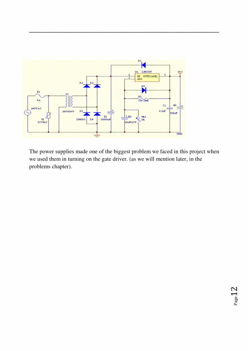
And one as Vcc for the IGBT gate driver, as shown below
The power supplies made one of the biggest problem we faced in this project when
we used them in turning on the gate driver. (as we will mention later, in the
problems chapter).
ـــــــــــــــــــــــــــــــــــــــــــــــــــــــــــــــــــــــــــــــــــــــــــــــــــــــــــــــــــــــــــــــــــــــــــــــــــــــــــــــــــــــــــــــــــــــــــــــــــــــــــــ
Pa
ge1
3
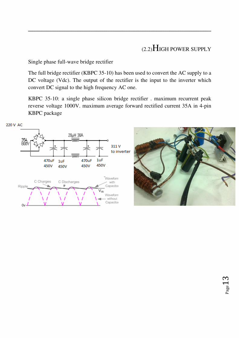
(2.2)HIGH POWER SUPPLY
Single phase full-wave bridge rectifier
The full bridge rectifier (KBPC 35-10) has been used to convert the AC supply to a
DC voltage (Vdc). The output of the rectifier is the input to the inverter which
convert DC signal to the high frequency AC one.
KBPC 35-10: a single phase silicon bridge rectifier . maximum recurrent peak
reverse voltage 1000V. maximum average forward rectified current 35A in 4-pin
KBPC package
ـــــــــــــــــــــــــــــــــــــــــــــــــــــــــــــــــــــــــــــــــــــــــــــــــــــــــــــــــــــــــــــــــــــــــــــــــــــــــــــــــــــــــــــــــــــــــــــــــــــــــــــ
Pa
ge1
4
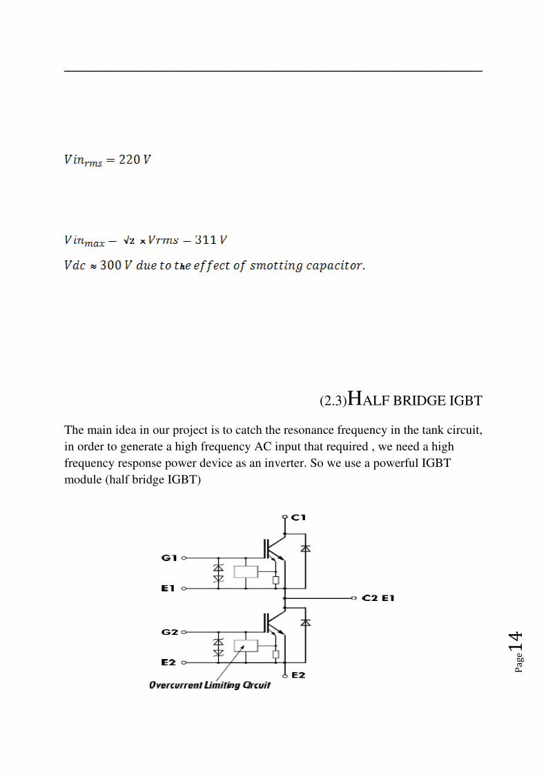
(2.3)HALF BRIDGE IGBT
The main idea in our project is to catch the resonance frequency in the tank circuit,
in order to generate a high frequency AC input that required , we need a high
frequency response power device as an inverter. So we use a powerful IGBT
module (half bridge IGBT)
ـــــــــــــــــــــــــــــــــــــــــــــــــــــــــــــــــــــــــــــــــــــــــــــــــــــــــــــــــــــــــــــــــــــــــــــــــــــــــــــــــــــــــــــــــــــــــــــــــــــــــــــ
Pa
ge1
5
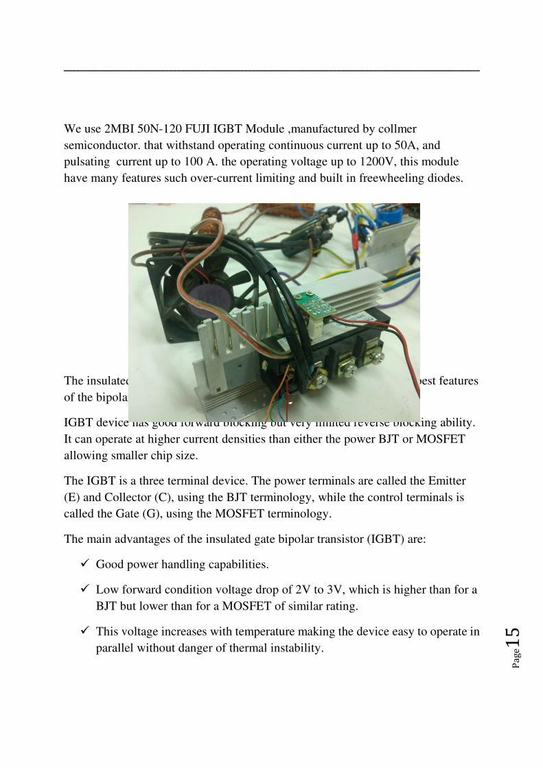
We use 2MBI 50N-120 FUJI IGBT Module ,manufactured by collmer
semiconductor. that withstand operating continuous current up to 50A, and
pulsating current up to 100 A. the operating voltage up to 1200V, this module
have many features such over-current limiting and built in freewheeling diodes.
The insulated gate bipolar transistor (IGBT) is an attempt to unite the best features
of the bipolar junction transistor and the MOSFET technologies.
IGBT device has good forward blocking but very limited reverse blocking ability.
It can operate at higher current densities than either the power BJT or MOSFET
allowing smaller chip size.
The IGBT is a three terminal device. The power terminals are called the Emitter
(E) and Collector (C), using the BJT terminology, while the control terminals is
called the Gate (G), using the MOSFET terminology.
The main advantages of the insulated gate bipolar transistor (IGBT) are:
� Good power handling capabilities.
� Low forward condition voltage drop of 2V to 3V, which is higher than for a
BJT but lower than for a MOSFET of similar rating.
� This voltage increases with temperature making the device easy to operate in
parallel without danger of thermal instability.

ـــــــــــــــــــــــــــــــــــــــــــــــــــــــــــــــــــــــــــــــــــــــــــــــــــــــــــــــــــــــــــــــــــــــــــــــــــــــــــــــــــــــــــــــــــــــــــــــــــــــــــــ
Pa
ge1
6
� High speed switching capability.
� Relatively simple voltage controlled gate driver.
� Lower gate current.
(2.4) PIC MICROCONTROLLER
In our project we use PIC Microcontroller (16F877A) as a square wave function
generator which is necessary to the input of the IGBT driver.
The circuit as shown below
The code in the appendix (B)
ـــــــــــــــــــــــــــــــــــــــــــــــــــــــــــــــــــــــــــــــــــــــــــــــــــــــــــــــــــــــــــــــــــــــــــــــــــــــــــــــــــــــــــــــــــــــــــــــــــــــــــــ
Pa
ge1
7
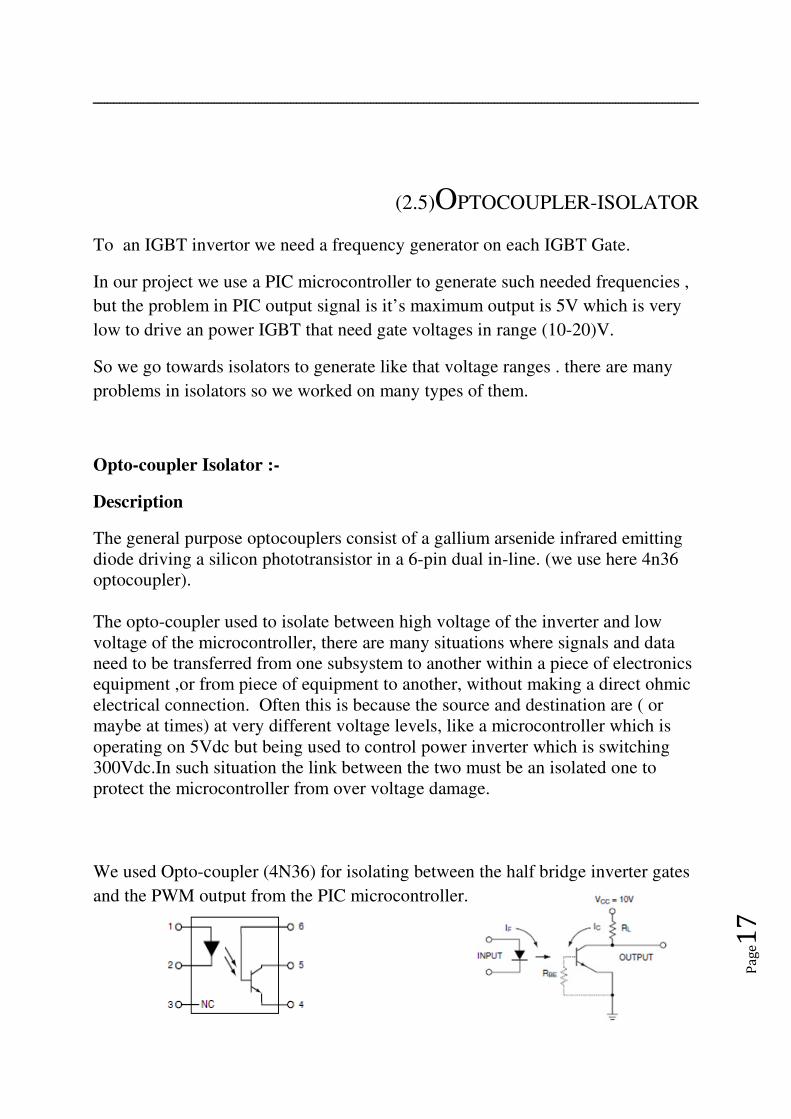
(2.5)OPTOCOUPLER-ISOLATOR
To an IGBT invertor we need a frequency generator on each IGBT Gate.
In our project we use a PIC microcontroller to generate such needed frequencies ,
but the problem in PIC output signal is it’s maximum output is 5V which is very
low to drive an power IGBT that need gate voltages in range (10-20)V.
So we go towards isolators to generate like that voltage ranges . there are many
problems in isolators so we worked on many types of them.
Opto-coupler Isolator :-
Description
The general purpose optocouplers consist of a gallium arsenide infrared emitting
diode driving a silicon phototransistor in a 6-pin dual in-line. (we use here 4n36
optocoupler).
The opto-coupler used to isolate between high voltage of the inverter and low
voltage of the microcontroller, there are many situations where signals and data
need to be transferred from one subsystem to another within a piece of electronics
equipment ,or from piece of equipment to another, without making a direct ohmic
electrical connection. Often this is because the source and destination are ( or
maybe at times) at very different voltage levels, like a microcontroller which is
operating on 5Vdc but being used to control power inverter which is switching
300Vdc.In such situation the link between the two must be an isolated one to
protect the microcontroller from over voltage damage.
We used Opto-coupler (4N36) for isolating between the half bridge inverter gates
and the PWM output from the PIC microcontroller.

ـــــــــــــــــــــــــــــــــــــــــــــــــــــــــــــــــــــــــــــــــــــــــــــــــــــــــــــــــــــــــــــــــــــــــــــــــــــــــــــــــــــــــــــــــــــــــــــــــــــــــــــ
Pa
ge1
8
(2.6)GATE DRIVERS……
IR2110-GATE DRIVER
Description
The IR2110/IR2113 are high voltage, high speed power
MOSFET and IGBT drivers with independent high and low side
referenced output Channels The output drivers feature a high
pulse current buffer stage designed for minimum driver cross-
conduction. Propagation delays are matched to simplify use in
high frequency applications. Floating channel designed for
bootstrap operation Fully operational to +500V or +600V
Tolerant to negative transient voltage dV/dt immune.
Configuration
After a lot of searching to find the solution for firing the upper IGBT in a proper
way,and Since the optocoupler circuit fail in carrying out that task (we will discuss
this later in problems chapter), we find that there is a lot of special IC’s that are
used to do that, one of them which we used it in our project is IR2110, really it is a
good IC to do that in efficient way .
The IR IC is a very a difficult one, but we challenge to turn it on and after a FOUR
weeks of suffering and making our experiment and testing on it….. Finally, we out
in the following connection, to let it work properly :
.
ـــــــــــــــــــــــــــــــــــــــــــــــــــــــــــــــــــــــــــــــــــــــــــــــــــــــــــــــــــــــــــــــــــــــــــــــــــــــــــــــــــــــــــــــــــــــــــــــــــــــــــــ
Pa
ge1
9
After a lot of search on a way to get this IC (since this IC not available in the local
markets) we bring two ICs from abroad country…… this suffering is not problem,
the main problem here is that when we carry out the first experiment on our
project, these ICs exploded in a terrible way……. And sadly, we couldn’t get this
IC again.
So we looked for another IC to replace that burned ICs, and we find another IC
which is called L6384E…..
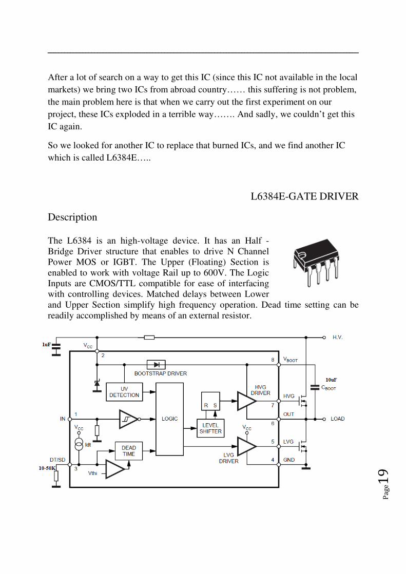
L6384E-GATE DRIVER
Description
The L6384 is an high-voltage device. It has an Half -
Bridge Driver structure that enables to drive N Channel
Power MOS or IGBT. The Upper (Floating) Section is
enabled to work with voltage Rail up to 600V. The Logic
Inputs are CMOS/TTL compatible for ease of interfacing
with controlling devices. Matched delays between Lower
and Upper Section simplify high frequency operation. Dead time setting can be
readily accomplished by means of an external resistor.
ـــــــــــــــــــــــــــــــــــــــــــــــــــــــــــــــــــــــــــــــــــــــــــــــــــــــــــــــــــــــــــــــــــــــــــــــــــــــــــــــــــــــــــــــــــــــــــــــــــــــــــــ
Pa
ge2
0
HIGH VOLTAGE RAIL UP TO 600 V
• dV/dt IMMUNITY +- 50 V/nsec IN FULL TEMPERATURE RANGE
• DRIVER CURRENT CAPABILITY:
400 mA SOURCE,
650 mA SINK
• SWITCHING TIMES 50/30 nsec RISE/FALL WITH 1nF LOAD
• CMOS/TTL SCHMITT TRIGGER INPUTS WITH HYSTERESIS AND
PULL DOWN
• SHUT DOWN INPUT
• DEAD TIME SETTING
• UNDER VOLTAGE LOCK OUT
• INTEGRATED BOOTSTRAP DIODE
• CLAMPING ON Vcc
• SO8/MINIDIP PACKAGES
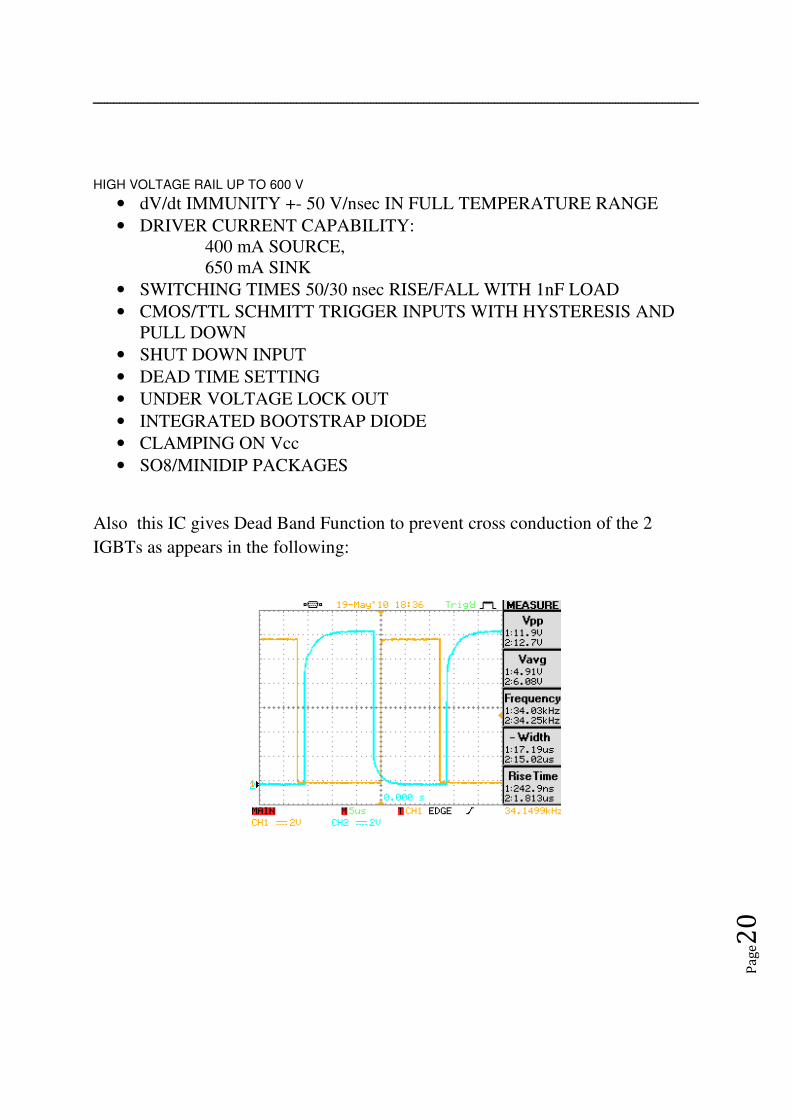
Also this IC gives Dead Band Function to prevent cross conduction of the 2
IGBTs as appears in the following:
ـــــــــــــــــــــــــــــــــــــــــــــــــــــــــــــــــــــــــــــــــــــــــــــــــــــــــــــــــــــــــــــــــــــــــــــــــــــــــــــــــــــــــــــــــــــــــــــــــــــــــــــ
Pa
ge2
1
(2.7)BOOTSTRAP CAPACITOR
A N-MOSFET/IGBT needs a significantly positive charge (VGS > Vth) applied to
the gate in order to turn on
A bootstrap capacitor is connected from the supply rail (V+) to the output voltage.
If the capacitor is polarized then the orientation of the capacitor is as follows:
Anode(marked with ‘+’)→(V+) and Cathode (marked with ‘-’)→Output. In other
words, the capacitor should be between the output (source of an N-MOSFET) and
(V+). Usually the source terminal of the N-MOSFET is connected to the cathode
of a recirculation diode allowing for efficient management of stored energy in the
typically inductive load .Due to the charge storage characteristics of a capacitor,
the bootstrap voltage will rise above (V+) providing the needed gate drive voltage
A MOSFET/IGBT is a voltage controlled device which, in theory, will not have
any gate current. This makes it possible to utilize the charge inside the capacitor
for control purposes. However, eventually the capacitor will lose its charge (due to
parasitic gate current and non ideal (i.e. infinite) internal resistance), so this
scheme is only used where there is a steady pulse present. This is because the
pulsing action allows for the capacitor to discharge (at least partially if not
completely). Most control schemes that use a bootstrap capacitor force the high
side driver (N-MOSFET) off for a minimum time to allow for the capacitor to
refill. This means that the duty cycle will always need to be less than 100% to
accommodate for the parasitic discharge unless the leakage is accommodated for in
another manner
How Does the high side driver support a high voltage IGBT?
Gate voltage for high side driver employs supply circuit comprising a bootstrap
diode and bootstrap capacitor (see the fig bellow). The bootstrap diode may be
ـــــــــــــــــــــــــــــــــــــــــــــــــــــــــــــــــــــــــــــــــــــــــــــــــــــــــــــــــــــــــــــــــــــــــــــــــــــــــــــــــــــــــــــــــــــــــــــــــــــــــــــ
Pa
ge2
2
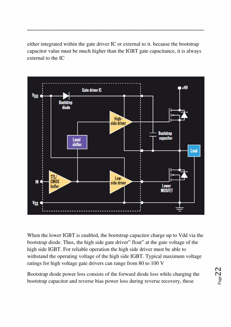
either integrated within the gate driver IC or external to it. because the bootstrap
capacitor value must be much higher than the IGBT gate capacitance, it is always
external to the IC
When the lower IGBT is enabled, the bootstrap capacitor charge up to Vdd via the
bootstrap diode. Thus, the high side gate driver” float” at the gate voltage of the
high side IGBT. For reliable operation the high side driver must be able to
withstand the operating voltage of the high side IGBT. Typical maximum voltage
ratings for high voltage gate drivers can range from 80 to 100 V
Bootstrap diode power loss consists of the forward diode loss while charging the
bootstrap capacitor and reverse bias power loss during reverse recovery, these

ـــــــــــــــــــــــــــــــــــــــــــــــــــــــــــــــــــــــــــــــــــــــــــــــــــــــــــــــــــــــــــــــــــــــــــــــــــــــــــــــــــــــــــــــــــــــــــــــــــــــــــــ
Pa
ge2
3
events occurs once per cycle, so this diode loss proportional to the switching
frequency
BOOTSTRAP CAPACITOR OPRATION & SELECTION
OPERATION:
* Vbs provides the supply to the high side driver circuitry of the control ICs. This
supply needed to be in range of 10-20 V.
* Vbs is floating supply.
* Two method to generate Vbs; one of these being the bootstrap method.
Advantage: simple & inexpensive.
Limitation: Duty cycle and on –times are limited by the requirement to refresh the
charge in the bootstrap capacitor (note. Long on –time and high duty cycle require
a CARGE PUMP CIRCUIT).
The operation of the circuit is as follows. When Vs is pulled down to ground
(either through the low side FET or the load. Depending on the circuit
ـــــــــــــــــــــــــــــــــــــــــــــــــــــــــــــــــــــــــــــــــــــــــــــــــــــــــــــــــــــــــــــــــــــــــــــــــــــــــــــــــــــــــــــــــــــــــــــــــــــــــــــ
Pa
ge2
4
configuration). The bootstrap capacitor(Cbs) charges through the bootstrap
capacitor diode (Dbs) from the 15V Vcc supply. Thus providing as supply to Vbs.
(2.8)MATCHING COIL
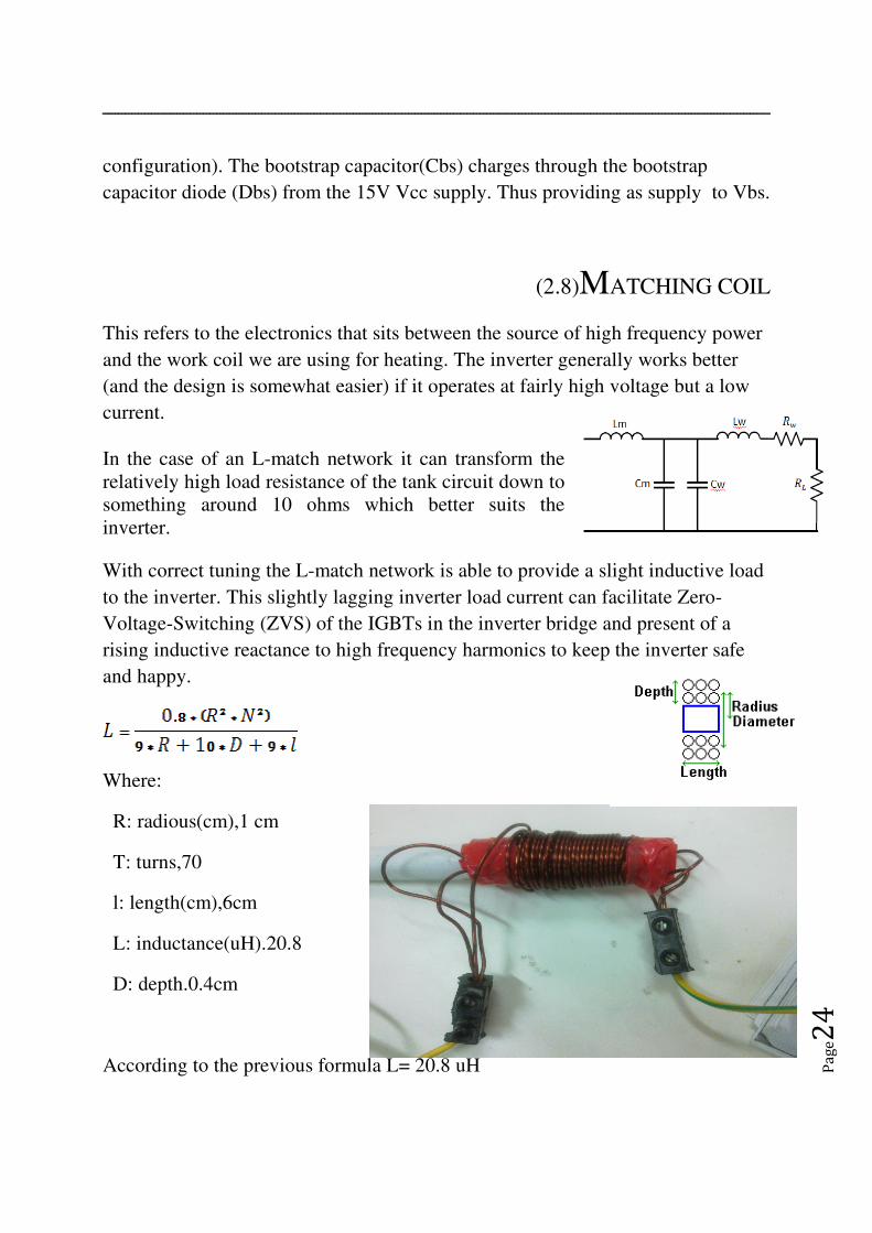
This refers to the electronics that sits between the source of high frequency power
and the work coil we are using for heating. The inverter generally works better
(and the design is somewhat easier) if it operates at fairly high voltage but a low
current.
In the case of an L-match network it can transform the
relatively high load resistance of the tank circuit down to
something around 10 ohms which better suits the
inverter.
With correct tuning the L-match network is able to provide a slight inductive load
to the inverter. This slightly lagging inverter load current can facilitate Zero-
Voltage-Switching (ZVS) of the IGBTs in the inverter bridge and present of a
rising inductive reactance to high frequency harmonics to keep the inverter safe
and happy.
Where:
R: radious(cm),1 cm
T: turns,70
l: length(cm),6cm
L: inductance(uH).20.8
D: depth.0.4cm
According to the previous formula L= 20.8 uH
ـــــــــــــــــــــــــــــــــــــــــــــــــــــــــــــــــــــــــــــــــــــــــــــــــــــــــــــــــــــــــــــــــــــــــــــــــــــــــــــــــــــــــــــــــــــــــــــــــــــــــــــ
Pa
ge2
5
according to the measuring device L= 20 uH (at low frequency)
L= 11 uH at high frequency.
(2.9)WORK COIL
coil design for induction heating is built upon a large store of empirical data.
Because of this, coil design is generally based on experience,
conditions that should be kept in mind when designing any coil for IH
*The coil should be coupled to the part as closely as feasible for maximum energy
transfer.
*The coil must be designed to prevent the cancellation of the magnetic field.
*The flux lines are concentrated inside the coil, providing the maximum heating
rate there.
Wheeler’s formula and the Specification of the work coil play the large role in
design the work coil.
� Wheeler’s formula
� Specification
ـــــــــــــــــــــــــــــــــــــــــــــــــــــــــــــــــــــــــــــــــــــــــــــــــــــــــــــــــــــــــــــــــــــــــــــــــــــــــــــــــــــــــــــــــــــــــــــــــــــــــــــ
Pa
ge2
6
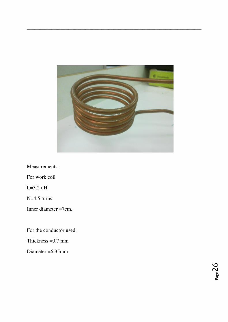
Measurements:
For work coil
L=3.2 uH
N=4.5 turns
Inner diameter =7cm.
For the conductor used:
Thickness =0.7 mm
Diameter =6.35mm
ـــــــــــــــــــــــــــــــــــــــــــــــــــــــــــــــــــــــــــــــــــــــــــــــــــــــــــــــــــــــــــــــــــــــــــــــــــــــــــــــــــــــــــــــــــــــــــــــــــــــــــــ
Pa
ge2
7
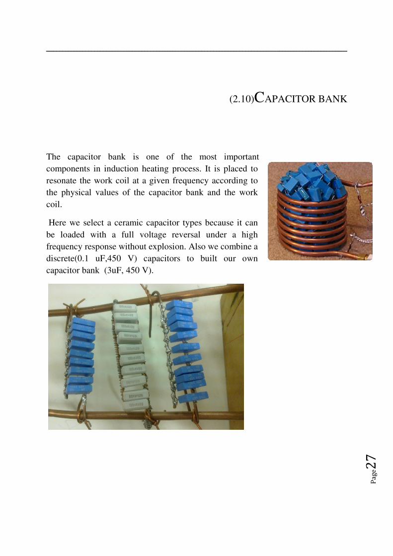
(2.10)CAPACITOR BANK
The capacitor bank is one of the most important
components in induction heating process. It is placed to
resonate the work coil at a given frequency according to
the physical values of the capacitor bank and the work
coil.
Here we select a ceramic capacitor types because it can
be loaded with a full voltage reversal under a high
frequency response without explosion. Also we combine a
discrete(0.1 uF,450 V) capacitors to built our own
capacitor bank (3uF, 450 V).

ـــــــــــــــــــــــــــــــــــــــــــــــــــــــــــــــــــــــــــــــــــــــــــــــــــــــــــــــــــــــــــــــــــــــــــــــــــــــــــــــــــــــــــــــــــــــــــــــــــــــــــــ
Pa
ge2
8
(2.11)WORK PIECE
The design specification is changed with changing the workpiece shape and type,
so the voltage and current in the resonant circuit will vary. In our project we want
to harden steel workpiece (1040 carbon steel).
� Specification

ـــــــــــــــــــــــــــــــــــــــــــــــــــــــــــــــــــــــــــــــــــــــــــــــــــــــــــــــــــــــــــــــــــــــــــــــــــــــــــــــــــــــــــــــــــــــــــــــــــــــــــــ
Pa
ge2
9

ـــــــــــــــــــــــــــــــــــــــــــــــــــــــــــــــــــــــــــــــــــــــــــــــــــــــــــــــــــــــــــــــــــــــــــــــــــــــــــــــــــــــــــــــــــــــــــــــــــــــــــــ
Pa
ge3
0
Chapter 3…PROPLEMS & CONSTRAINTS
PART
While implementing the project stages, so many tough problems faced us. So, in
this chapter each problem or constrains is illustrated deeply. Also we’ll explained
how we solved everyone.
Mismatching between PIC microcontroller and IGBT gate.
In our project we use an inverter to alter the DC level that represent the input of the
inverter to a high frequency output signal.
To drive this inverter we supposed to use one of the output of the PIC
microcontroller as a square wave generation. The problem appeared in VGE
threshold voltage of the IGBTs used since the PIC give us a voltage level only 0 or
5V .
solution
At first we used the opto-coupler as an IGBT gate drive , because it is the simplest
way to isolate high voltage level from low voltage one. By adjusting the collector
voltage of the right side of the opto-coupler.

ـــــــــــــــــــــــــــــــــــــــــــــــــــــــــــــــــــــــــــــــــــــــــــــــــــــــــــــــــــــــــــــــــــــــــــــــــــــــــــــــــــــــــــــــــــــــــــــــــــــــــــــ
Pa
ge3
1
Opto-coupler Constrains.
after we installed this circuit we discovered that this isolator can drive only a
discrete IGBT and since we drive a model of IGBT (half bridge model), the isolator
is not sufficient to drive like that model of IGBTs.
the problem is when we drive half IGBT inverter the lower IGBT is work, but the
higher one didn't work , because the emitter is floating and there is no reference to
the opto-coupler.
in the other hand we faced that when we increase the frequency of the opto-cpupler
input pulses signal, we amazed that the output is clipping until vanish (as
increasing the frequency).
Partly Solution:-
After a hard experiments we discovered that the problem is biasing one, and the
solution is by changing (increasing about 330 ohm) the collector resistor we
obtained a wider range of frequency response (about 8 KHz to catch the output).
But the main problem for the upper IGBT still not solve by using Opto-coupler so
we look for use another special circuit configuration which called IGBT IC gate
driver, which will solve this problem.
IR FAILURE.
We installed the recommended circuit mention in the data sheet of the IR2110 but
it didn’t work correctly, despite of we connect the recommended circuit exactly as
mentioned….It still doesn’t work
Solution:-
We find this series of IR ICs doesn’t work if not the logic GND supply of the PIC
microcontroller and power GND supply are not separated from each others. So
we have to separate them. (use two different power supplies for each ).

ـــــــــــــــــــــــــــــــــــــــــــــــــــــــــــــــــــــــــــــــــــــــــــــــــــــــــــــــــــــــــــــــــــــــــــــــــــــــــــــــــــــــــــــــــــــــــــــــــــــــــــــ
Pa
ge3
2
PIC microcontroller failure
We faced two problems in programming PIC microcontroller
First one is summarized in the programming command, since there is a command
function (delay_us();) this function take an integer value only, and our project deal
with a variable frequency.
Second one summarized in the following thing.
That when we give the PIC microcontroller a command to take an output of
driving square wave, we surprised with the result which is not in the same
command, it give a percentage of error which increase with increasing the input
frequency(i.e. when order the PIC microcontroller to give an output squre wave
with f=10 KHz , it give about 9 KHz)
Solution:
After making some calculations on the operating frequency we make a type
casting form the float number to an integer one.
About the second problem is still not solved because we think that this problem
depends on the external connection of the basic circuit.

ـــــــــــــــــــــــــــــــــــــــــــــــــــــــــــــــــــــــــــــــــــــــــــــــــــــــــــــــــــــــــــــــــــــــــــــــــــــــــــــــــــــــــــــــــــــــــــــــــــــــــــــ
Pa
ge3
3
Chapter 4…Cost
PART COST(NIC.)
BRIDGE RECTIFIER( KBPC 35-10) 50
2 CAPACITORS (470uF,450V) 60
3 INDUCTORS (20 uH,30 Amp) 30
IGBT MODULE(2MBI 50N-120) 150
BASIC CIRCUIT FOR PIC 60
PIC 16F877A 30
40 CAPACITOR (0.1uF,450V) 120
WORK COIL (3.2uH,200AMP) 50
GATE DRIVER(IR 1110) 100
LOW VOLTAGE POWER SUPPLYs 100
HEAT SINKERS 30
FAN+THERMOCOUPLER SINSOR 50
∑ 830

ـــــــــــــــــــــــــــــــــــــــــــــــــــــــــــــــــــــــــــــــــــــــــــــــــــــــــــــــــــــــــــــــــــــــــــــــــــــــــــــــــــــــــــــــــــــــــــــــــــــــــــــ
Pa
ge3
4
Chapter 5…Conclusion
For this project Induction Heating we use a Hardware that is associated with
appropriate Software in order to do the job.
It was discovered that during the project that there are several problems with
implementing Induction Heating technique as shown previously.
Using IGBT switches as an inverter was more reliable and enjoyable from using
BJTs, since driving circuit for the last one is almost disappeared in presence of
other rugged switches.
Also we conclude practical work differs a lot from theoretical one, although they
can not be separate from each other.
The Induction Heating concept is the same for all the application.
And most important, no matter what happen for our mental state while working in
this project, WE LEARN A LOT ABUOT EVERY THING,
ـــــــــــــــــــــــــــــــــــــــــــــــــــــــــــــــــــــــــــــــــــــــــــــــــــــــــــــــــــــــــــــــــــــــــــــــــــــــــــــــــــــــــــــــــــــــــــــــــــــــــــــ
Pa
ge3
5
Chapter -6-…Recommendation Part
RECOMMENDATIONS
After a lot of stress and fatigue in implementing this project, we recommend the
following, hoping for everyone a good life and health with existence of
“INDUCTION HEATING”:
� First of all we DON’T recommend anyone, anywhere, for any purpose to
experiment with the work of this project again. The reason is that one may
need a whole year –maybe two- just to understand the theoretical aspects
that are embedded in this kind of subjects. Another year for doing the
practical part including hardware and software, while maintaining health
care above everything☺.
� Don’t ever, never, let any exposed wires or any exposed charged capacitors
in your circuits. You will defiantly regret doing this.
� Make sure that grounds in your circuit (high side and low side grounds) are
completely separated from each other, IT IS A MATTER OF LIFE AND
DEATH.
� Always DOUBLE CHECK on your work before turning on any supply,
because from an important & expensive part in your circuit might be ON
FIRE!
� Don’t be disappointed, LIFE IS HARD!
ـــــــــــــــــــــــــــــــــــــــــــــــــــــــــــــــــــــــــــــــــــــــــــــــــــــــــــــــــــــــــــــــــــــــــــــــــــــــــــــــــــــــــــــــــــــــــــــــــــــــــــــ
Pa
ge3
6
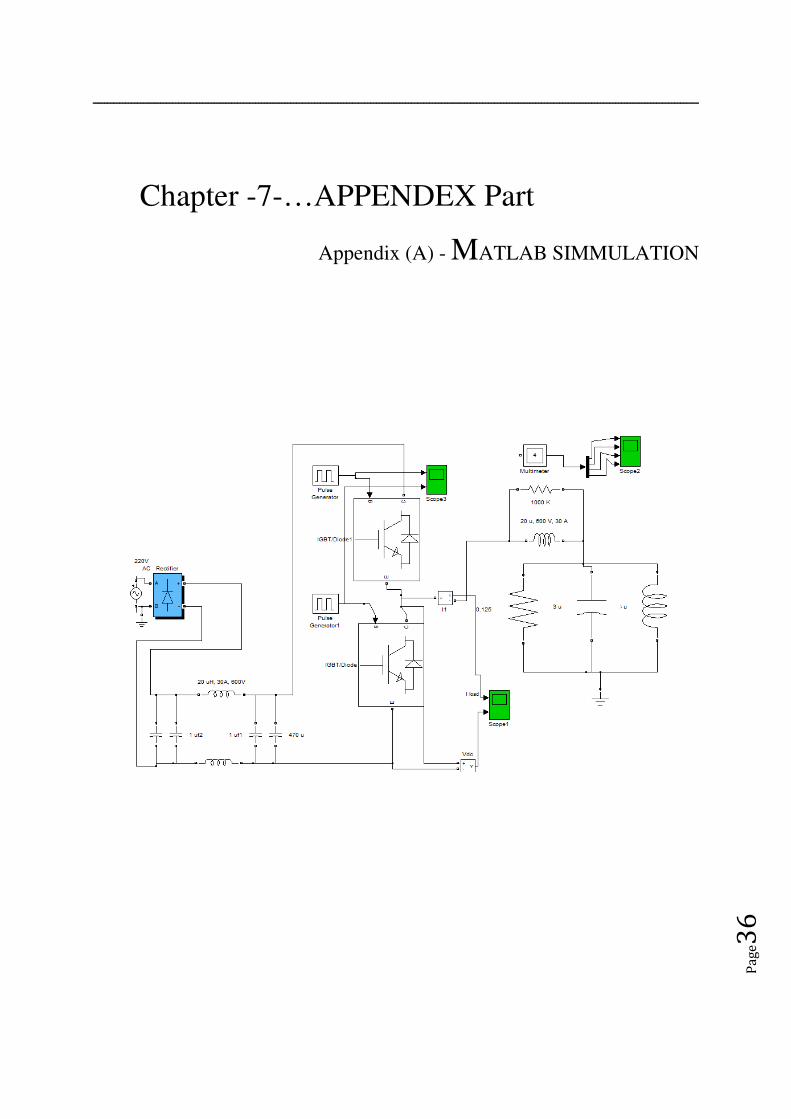
Chapter -7-…APPENDEX Part
Appendix (A) - MATLAB SIMMULATION

ـــــــــــــــــــــــــــــــــــــــــــــــــــــــــــــــــــــــــــــــــــــــــــــــــــــــــــــــــــــــــــــــــــــــــــــــــــــــــــــــــــــــــــــــــــــــــــــــــــــــــــــ
Pa
ge3
7
Appendix (B) – PIC PROGRAMMIN
Software program on PIC C
#include "C:\Users\QADRIII\Desktop\proj 50000\proj 50.h"
#include <math.h>
#include <string.h>
int i=0;
long cci(char c[]){
float num=0;
for(i=0;i<(strlen(c));i++){
printf("%c",c[i]);
}
for(i=0;i<(strlen(c));i++){
if(c[i]>='0' && c[i]<='9' ){
num = num * 10 ;
num=num+(c[i] - 48);
printf("hi");
printf("%f",num);

ـــــــــــــــــــــــــــــــــــــــــــــــــــــــــــــــــــــــــــــــــــــــــــــــــــــــــــــــــــــــــــــــــــــــــــــــــــــــــــــــــــــــــــــــــــــــــــــــــــــــــــــ
Pa
ge3
8
}
}
printf("final");
printf("%f",num);
return num;
}
void main()
{
float freq=0;
float duty=0;
char freqq[6]=" ";
char dtyy[2]=" ";
char x='r';
int count1=0;
float high=0;
float low=0;

ـــــــــــــــــــــــــــــــــــــــــــــــــــــــــــــــــــــــــــــــــــــــــــــــــــــــــــــــــــــــــــــــــــــــــــــــــــــــــــــــــــــــــــــــــــــــــــــــــــــــــــــ
Pa
ge3
9
int32 high1=0;
int32 low1=0;
char m='q';
loop1:
setup_adc_ports(NO_ANALOGS);
setup_adc(ADC_OFF);
setup_psp(PSP_DISABLED);
setup_spi(FALSE);
setup_timer_0(RTCC_INTERNAL|RTCC_DIV_1);
setup_timer_1(T1_DISABLED);
setup_timer_2(T2_DISABLED,0,1);
setup_comparator(NC_NC_NC_NC);
setup_vref(FALSE);
m='q';
x='r';
high=0;
low=0;
high1=0;
low1=0;
freq=0;
duty=0;

ـــــــــــــــــــــــــــــــــــــــــــــــــــــــــــــــــــــــــــــــــــــــــــــــــــــــــــــــــــــــــــــــــــــــــــــــــــــــــــــــــــــــــــــــــــــــــــــــــــــــــــــ
Pa
ge4
0
// TODO: USER CODE!!
while(true){
while(x!='s'){ //to stop intering if s
printf("input freq \n\r");
while(!kbhit())
restart_wdt();
if (kbhit()){
x=getc();
printf("%c",x);
if(x!='s')
{
freqq[count1]=x;
count1++;
}
}
}
count1=0;
freq=cci(freqq);
printf("freq= %f\n\r",freq);

ـــــــــــــــــــــــــــــــــــــــــــــــــــــــــــــــــــــــــــــــــــــــــــــــــــــــــــــــــــــــــــــــــــــــــــــــــــــــــــــــــــــــــــــــــــــــــــــــــــــــــــــ
Pa
ge4
1
while(x!='t'){ //to stop intering if t
printf("input duty \n\r");
while(!kbhit())
restart_wdt();
if(kbhit()){
x=getc();
printf("%c",x);
if(x!='t')
{
dtyy[count1]=x;
count1++;
}
}
}
count1=0;
duty=cci(dtyy);
printf("duty= %f\n\r",duty);
restart_wdt();
if(freq > 0 && duty > 0){
freq=(1.0/freq);
freq=freq*1000000.0;

ـــــــــــــــــــــــــــــــــــــــــــــــــــــــــــــــــــــــــــــــــــــــــــــــــــــــــــــــــــــــــــــــــــــــــــــــــــــــــــــــــــــــــــــــــــــــــــــــــــــــــــــ
Pa
ge4
2
printf("freq=%f\n\r",freq);
high = (duty/100.0)*freq;
high1=high;
low = freq-high;
low1=low;
restart_wdt();
while(m!='E'){
restart_wdt();
output_high(pin_D1);
output_low(pin_D0);
delay_us(high1);
output_low(pin_D1);
output_high(pin_D0);
delay_us(low1);
if(kbhit()){
m=getc();
}
if(m =='E')
{
goto loop1;
}

ـــــــــــــــــــــــــــــــــــــــــــــــــــــــــــــــــــــــــــــــــــــــــــــــــــــــــــــــــــــــــــــــــــــــــــــــــــــــــــــــــــــــــــــــــــــــــــــــــــــــــــــ
Pa
ge4
3
}}}}