
T302 - d2lxe0fofddnat.cloudfront.net · 0.5-4.0 GHz 1W High Power Amplifier T302 1 Rev. eRex...
23
0.5-4.0 GHz 1W High Power Amplifier BT302 1 Rev. C BeRex ●website: www.berex.com ●email: [email protected] Specificaons and informaon are subject to change and products may be disconnued without noce. BeRex is a trademark of BeRex. All other trademarks are the property of their respecve owners. © 2018 BeRex The BT302 is a high performance and a high dynamic range amplifier in a low cost sur- face mount package(SOT-89) with a RoHS- compliant, that incorporates reliable hetero- juncon-bipolar-transistor (HBT) devices fabricated with InGaP/GaAs technology. This device is designed for use where high linearity is required and features high ACLR and P1 performance with low consumpon current(215mA) and requires a few external matching components, DC blocking capaci- tors on the In/Output pin and a bypass ca- pacitor and a RF choke for the out port. Product Descripon Device Features 1 Device performance _ measured on a BeRex evaluaon board at 25°C, 50 Ω 2 OIP3 _ measured on two tones with a output power 16dBm/ tone , F2—F1 = 1 MHz.. Typical Performance 1 Parameter Frequency Unit 915 1960 2140 2400 2600 MHz 3500 Gain 22.0 17.5 17.0 16.0 15.3 dB 13.2 S11 -27.5 -19.5 -19.4 -32.8 -22.6 dB -22.7 S22 -13.0 -11.5 -17.3 -14.0 -14.8 dB -19.5 OIP3 2 41.8 41.5 41.8 42.1 41.3 dBm 40.8 P1dB 29.5 29.6 29.3 29.5 29.5 dBm 29.2 LTE 20M ACLR 18.5 19.1 19.1 19.1 19.2 dBm 18.5 WCDMA ACLR 19.2 19.5 19.4 19.2 19.3 dBm 18.5 Noise Figure 4.1 4.1 4.2 4.2 4.2 dB 4.3 Min. Typical Max. Unit Bandwidth 500 4000 MHz I cq @ (Vcc&Vbias=5V) 195 215 235 mA V CC /V bias 5.0 V R TH 19.5 °C/W Applicaon Circuits *ACLR Channel Power measured at -50dBc. - WCDMA set-up: 3GPP WCDMA, TM1+64DPCH, +5MHz offset, PAR 9.78 at 0.01% Prob. • Base staon /Repeaters Infrastructure/Small Cell • Commercial/Industrial/Military wireless system • LTE / WCDMA /CDMA Wireless Infrastructure Applicaons Absolute Maximum Rangs Parameter Unit Rang Operang Case Temperature °C -40 to +105 Storage Temperature °C -55 to +155 Juncon Temperature °C 220 Operang Voltage V +6.0 Supply Current mA 550 Input RF Power dBm 24 *Operaon of this device above any of these parameters may result in permanent damage. - LTE set-up: 3GPP LTE, FDD E-TM3.1, 20MHz BW, ±5MHz offset, PAR 9.75 @0.01% Prob. *External matching circuit: Refer to applicaon circuit for each frequency. • +5V/215mA at operang bias condion • Gain = 16.0 dB @ 2400MHz • P1dB = 29.5 dBm @ 2400MHz • OIP3 = 42.1dBm 16dBm/tone at 2400MHz • LTE 20M ACLR = 19.1dBm Output Power at -50dBc @ 2400MHz • Lead-free/Green/RoHS-compliant SOT89 SMT package
Transcript of T302 - d2lxe0fofddnat.cloudfront.net · 0.5-4.0 GHz 1W High Power Amplifier T302 1 Rev. eRex...
0.5-4.0 GHz 1W High Power Amplifier
BT302
1
Rev. C
BeRex website: www.berex.com email: [email protected]
Specifications and information are subject to change and products may be discontinued without notice. BeRex is a trademark of BeRex.
All other trademarks are the property of their respective owners. © 2018 BeRex
The BT302 is a high performance and a high
dynamic range amplifier in a low cost sur-
face mount package(SOT-89) with a RoHS-
compliant, that incorporates reliable hetero-
junction-bipolar-transistor (HBT) devices
fabricated with InGaP/GaAs technology.
This device is designed for use where high
linearity is required and features high ACLR
and P1 performance with low consumption
current(215mA) and requires a few external
matching components, DC blocking capaci-
tors on the In/Output pin and a bypass ca-
pacitor and a RF choke for the out port.
Product Description
Device Features
1 Device performance _ measured on a BeRex evaluation board at 25°C, 50 Ω 2 OIP3 _ measured on two tones with a output power 16dBm/ tone , F2—F1 = 1 MHz..
Typical Performance1
Parameter Frequency Unit
915 1960 2140 2400 2600 MHz 3500
Gain 22.0 17.5 17.0 16.0 15.3 dB 13.2
S11 -27.5 -19.5 -19.4 -32.8 -22.6 dB -22.7
S22 -13.0 -11.5 -17.3 -14.0 -14.8 dB -19.5
OIP32 41.8 41.5 41.8 42.1 41.3 dBm 40.8
P1dB 29.5 29.6 29.3 29.5 29.5 dBm 29.2
LTE 20M ACLR 18.5 19.1 19.1 19.1 19.2 dBm 18.5
WCDMA ACLR 19.2 19.5 19.4 19.2 19.3 dBm 18.5
Noise Figure 4.1 4.1 4.2 4.2 4.2 dB 4.3
Min. Typical Max. Unit
Bandwidth 500 4000 MHz
Icq @ (Vcc&Vbias=5V) 195 215 235 mA
VCC/Vbias 5.0 V
RTH 19.5 °C/W
Application Circuits
*ACLR Channel Power measured at -50dBc.
- WCDMA set-up: 3GPP WCDMA, TM1+64DPCH, +5MHz offset, PAR 9.78 at 0.01% Prob.
• Base station /Repeaters Infrastructure/Small Cell
• Commercial/Industrial/Military wireless system
• LTE / WCDMA /CDMA Wireless Infrastructure
Applications
Absolute Maximum Ratings
Parameter Unit Rating
Operating Case Temperature °C -40 to +105
Storage Temperature °C -55 to +155
Junction Temperature °C 220
Operating Voltage V +6.0
Supply Current mA 550
Input RF Power dBm 24
*Operation of this device above any of these parameters may result in permanent damage.
- LTE set-up: 3GPP LTE, FDD E-TM3.1, 20MHz BW, ±5MHz offset, PAR 9.75 @0.01% Prob.
*External matching circuit: Refer to application circuit for each frequency.
• +5V/215mA at operating bias condition • Gain = 16.0 dB @ 2400MHz • P1dB = 29.5 dBm @ 2400MHz • OIP3 = 42.1dBm 16dBm/tone at 2400MHz • LTE 20M ACLR = 19.1dBm Output Power at -50dBc @ 2400MHz
• Lead-free/Green/RoHS-compliant SOT89 SMT package
0.5-4.0 GHz 1W High Power Amplifier
BT302
2
Rev. C
BeRex website: www.berex.com email: [email protected]
Specifications and information are subject to change and products may be discontinued without notice. BeRex is a trademark of BeRex.
All other trademarks are the property of their respective owners. © 2018 BeRex
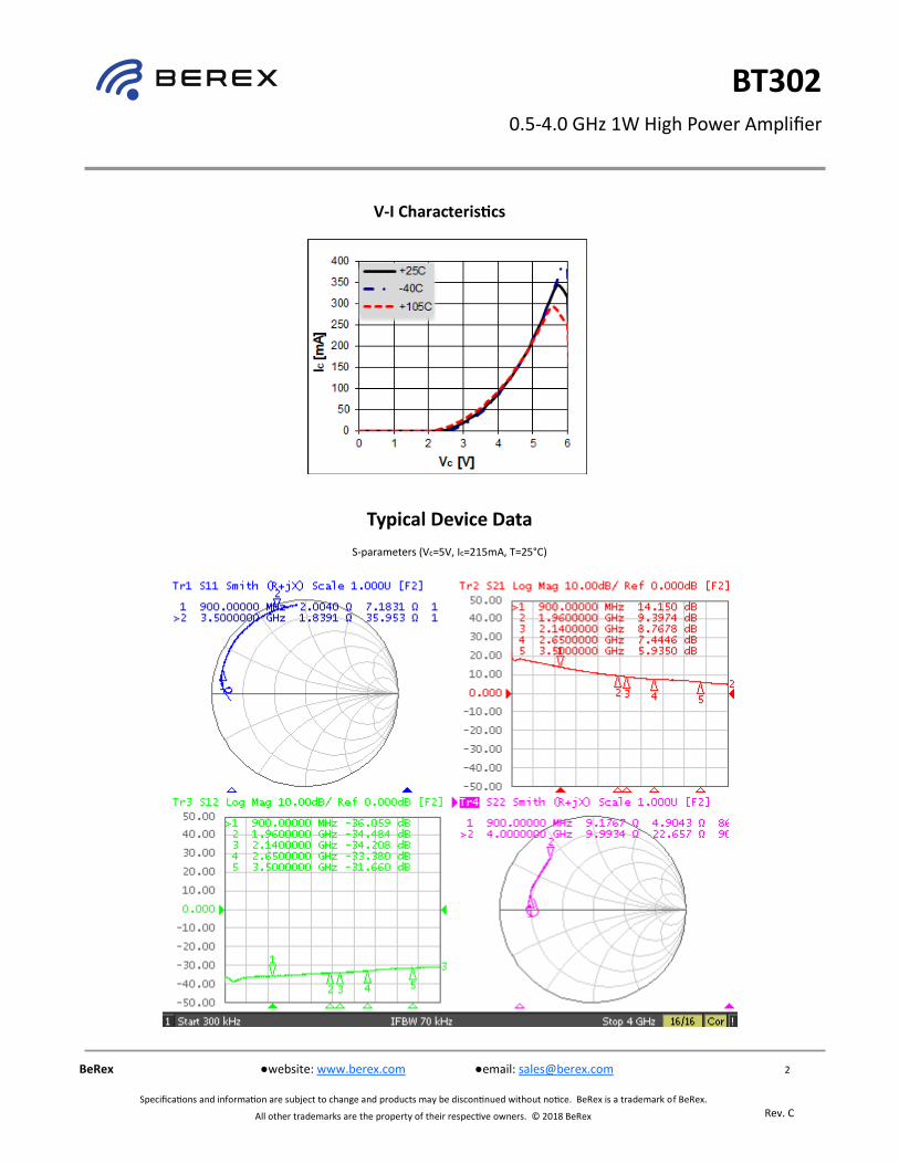
V-I Characteristics
Typical Device Data
S-parameters (Vc=5V, Ic=215mA, T=25°C)

0.5-4.0 GHz 1W High Power Amplifier
BT302
3
Rev. C
BeRex website: www.berex.com email: [email protected]
Specifications and information are subject to change and products may be discontinued without notice. BeRex is a trademark of BeRex.
All other trademarks are the property of their respective owners. © 2018 BeRex
S-Parameter (Vdevice = 5.0V, Ic = 215mA, T = 25 °C, calibrated to device leads)
Freq S11 S11 S21 S21 S12 S12 S22 S22
[MHz] [Mag] [Ang] [Mag] [Ang] [Mag] [Ang] [Mag] [Ang]
500 0.91 172.90 6.65 135.78 0.015 11.72 0.70 173.01
600 0.91 170.31 6.23 129.10 0.015 10.72 0.69 171.51
700 0.92 168.00 5.84 123.25 0.015 11.65 0.69 170.18
800 0.92 165.60 5.47 117.61 0.016 11.53 0.69 169.26
900 0.92 163.61 5.10 112.46 0.016 11.72 0.69 168.35
1000 0.93 161.62 4.76 108.08 0.016 13.86 0.69 167.44
1100 0.93 159.83 4.45 104.06 0.016 14.48 0.70 166.46
1200 0.93 158.14 4.18 100.16 0.016 14.53 0.70 165.67
1300 0.93 156.58 3.96 96.31 0.017 14.31 0.70 164.94
1400 0.93 154.90 3.77 93.11 0.017 14.97 0.70 164.19
1500 0.94 153.12 3.57 89.90 0.018 14.61 0.70 163.57
1600 0.94 151.63 3.43 86.54 0.018 15.01 0.70 162.55
1700 0.94 150.34 3.26 83.68 0.018 14.36 0.70 161.77
1800 0.94 148.55 3.14 80.43 0.019 15.13 0.70 160.93
1900 0.94 146.83 3.01 77.25 0.019 14.47 0.70 160.22
2000 0.94 145.20 2.89 74.02 0.019 13.74 0.70 159.29
2100 0.95 143.19 2.79 71.03 0.019 12.40 0.69 158.14
2200 0.94 141.46 2.69 68.15 0.020 13.77 0.69 156.91
2300 0.94 139.38 2.59 65.72 0.020 14.15 0.69 155.94
2400 0.95 136.88 2.52 63.57 0.020 13.40 0.69 154.78
2500 0.94 135.06 2.44 60.76 0.021 12.19 0.69 153.38
2600 0.95 132.76 2.40 58.88 0.022 12.17 0.69 151.92
2700 0.95 130.47 2.34 56.69 0.022 13.21 0.68 150.86
2800 0.95 127.90 2.31 53.61 0.023 12.11 0.68 149.05
2900 0.95 125.20 2.29 50.59 0.024 9.70 0.68 147.56
3000 0.95 122.86 2.27 47.41 0.025 9.36 0.69 145.83
3100 0.95 119.89 2.23 44.51 0.025 9.71 0.69 144.11
3200 0.95 116.94 2.13 40.75 0.025 6.11 0.69 142.53
3300 0.95 114.13 2.11 36.73 0.026 5.00 0.69 140.79
3400 0.95 111.26 2.05 33.66 0.026 4.11 0.69 139.25
3500 0.95 108.49 1.98 30.66 0.026 1.98 0.69 137.21
3600 0.95 105.74 1.92 27.79 0.027 1.21 0.70 135.77
3700 0.95 102.74 1.86 25.27 0.027 0.57 0.70 134.23
3800 0.95 100.24 1.83 22.61 0.027 -0.77 0.71 132.66
3900 0.96 97.55 1.76 20.97 0.028 -2.34 0.71 131.13
4000 0.96 95.01 1.71 17.13 0.027 -5.09 0.72 129.78
0.5-4.0 GHz 1W High Power Amplifier
BT302
4
Rev. C
BeRex website: www.berex.com email: [email protected]
Specifications and information are subject to change and products may be discontinued without notice. BeRex is a trademark of BeRex.
All other trademarks are the property of their respective owners. © 2018 BeRex
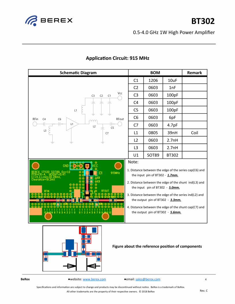
Application Circuit: 915 MHz
Schematic Diagram BOM Remark
C1 10uF 1206
C2 1nF 0603
C3 100pF 0603
C4 100pF 0603
C5 100pF 0603
C6 6pF 0603
C7 4.7pF 0603
L1 0805 39nH Coil
L2 2.7nH 0603
L3 0603 2.7nH
U1 BT302 SOT89
Note:
1. Distance between the edge of the series cap(C6) and
the input pin of BT302 - 1.7mm.
2. Distance between the edge of the shunt ind(L3) and
the input pin of BT302 - 5.0mm.
3. Distance between the edge of the series ind(L2) and
the output pin of BT302 - 3.3mm.
4. Distance between the edge of the shunt cap(C7) and
the output pin of BT302 - 5.6mm.
U1
C4
L1
C3 C2 C1
C5
RFin RFout
Vcc
L2
C7L3
C6
Figure about the reference position of components

0.5-4.0 GHz 1W High Power Amplifier
BT302
5
Rev. C
BeRex website: www.berex.com email: [email protected]
Specifications and information are subject to change and products may be discontinued without notice. BeRex is a trademark of BeRex.
All other trademarks are the property of their respective owners. © 2018 BeRex
Vc = 5V, Ic = 215mA
Typical Performance

0.5-4.0 GHz 1W High Power Amplifier
BT302
6
Rev. C
BeRex website: www.berex.com email: [email protected]
Specifications and information are subject to change and products may be discontinued without notice. BeRex is a trademark of BeRex.
All other trademarks are the property of their respective owners. © 2018 BeRex
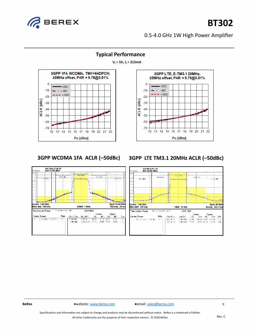
3GPP WCDMA 1FA ACLR (–50dBc) 3GPP LTE TM3.1 20MHz ACLR (–50dBc)
Vc = 5V, Ic = 215mA
Typical Performance

0.5-4.0 GHz 1W High Power Amplifier
BT302
7
Rev. C
BeRex website: www.berex.com email: [email protected]
Specifications and information are subject to change and products may be discontinued without notice. BeRex is a trademark of BeRex.
All other trademarks are the property of their respective owners. © 2018 BeRex
Application Circuit: 1960 MHz
Schematic Diagram BOM Remark
C1 1206 10uF
C2 0603 1nF
C3 0603 100pF
C4 0603 100pF
C5 0603 100pF
C6 0603 2.7pF
C7 0603 3.5pF
C8 0603 2pF
L1 0805 27nH Coil
U1 SOT89 BT302
Note:
1. Distance between the edge of the series cap(C6) and
the input pin of BT302 - 1.7mm.
2. Distance between the edge of the shunt ind(C7) and
the input pin of BT302 - 5.0mm.
3. Distance between the edge of the shunt cap(C8) and
the output pin of BT302 - 3.6mm.
Figure about the reference position of components
U1
C4
L1
C3 C2 C1
C5
RFin RFout
Vcc
C8C7
C6

0.5-4.0 GHz 1W High Power Amplifier
BT302
8
Rev. C
BeRex website: www.berex.com email: [email protected]
Specifications and information are subject to change and products may be discontinued without notice. BeRex is a trademark of BeRex.
All other trademarks are the property of their respective owners. © 2018 BeRex
Vc = 5V, Ic = 215mA
Typical Performance
0.5-4.0 GHz 1W High Power Amplifier
BT302
9
Rev. C
BeRex website: www.berex.com email: [email protected]
Specifications and information are subject to change and products may be discontinued without notice. BeRex is a trademark of BeRex.
All other trademarks are the property of their respective owners. © 2018 BeRex
3GPP WCDMA 1FA ACLR (–50dBc) 3GPP LTE TM3.1 20MHz ACLR (–50dBc)
Vc = 5V, Ic = 215mA
Typical Performance

0.5-4.0 GHz 1W High Power Amplifier
BT302
10
Rev. C
BeRex website: www.berex.com email: [email protected]
Specifications and information are subject to change and products may be discontinued without notice. BeRex is a trademark of BeRex.
All other trademarks are the property of their respective owners. © 2018 BeRex
Application Circuit: 2140 MHz
Schematic Diagram BOM Remark
C1 1206 10uF
C2 0603 1nF
C3 0603 100pF
C4 0603 100pF
C5 0603 100pF
C6 0603 2pF
C7 0603 2.5pF
C8 0805 1.5pF
L1 0603 20nH Coil
U1 SOT89 BT302
Note:
1. Distance between the edge of the series cap(C6) and
the input pin of BT302 - 1.7mm.
2. Distance between the edge of the shunt ind(C7) and
the input pin of BT302 - 5.6mm.
3. Distance between the edge of the shunt cap(C8) and
the output pin of BT302 - 3.3mm.
Figure about the reference position of components
U1
C4
L1
C3 C2 C1
C5
RFin RFout
Vcc
C8C7
C6

0.5-4.0 GHz 1W High Power Amplifier
BT302
11
Rev. C
BeRex website: www.berex.com email: [email protected]
Specifications and information are subject to change and products may be discontinued without notice. BeRex is a trademark of BeRex.
All other trademarks are the property of their respective owners. © 2018 BeRex
Vc = 5V, Ic = 215mA
Typical Performance

0.5-4.0 GHz 1W High Power Amplifier
BT302
12
Rev. C
BeRex website: www.berex.com email: [email protected]
Specifications and information are subject to change and products may be discontinued without notice. BeRex is a trademark of BeRex.
All other trademarks are the property of their respective owners. © 2018 BeRex
3GPP WCDMA 1FA ACLR (–50dBc) 3GPP LTE TM3.1 20MHz ACLR (–50dBc)
Vc = 5V, Ic = 215mA
Typical Performance
0.5-4.0 GHz 1W High Power Amplifier
BT302
13
Rev. C
BeRex website: www.berex.com email: [email protected]
Specifications and information are subject to change and products may be discontinued without notice. BeRex is a trademark of BeRex.
All other trademarks are the property of their respective owners. © 2018 BeRex
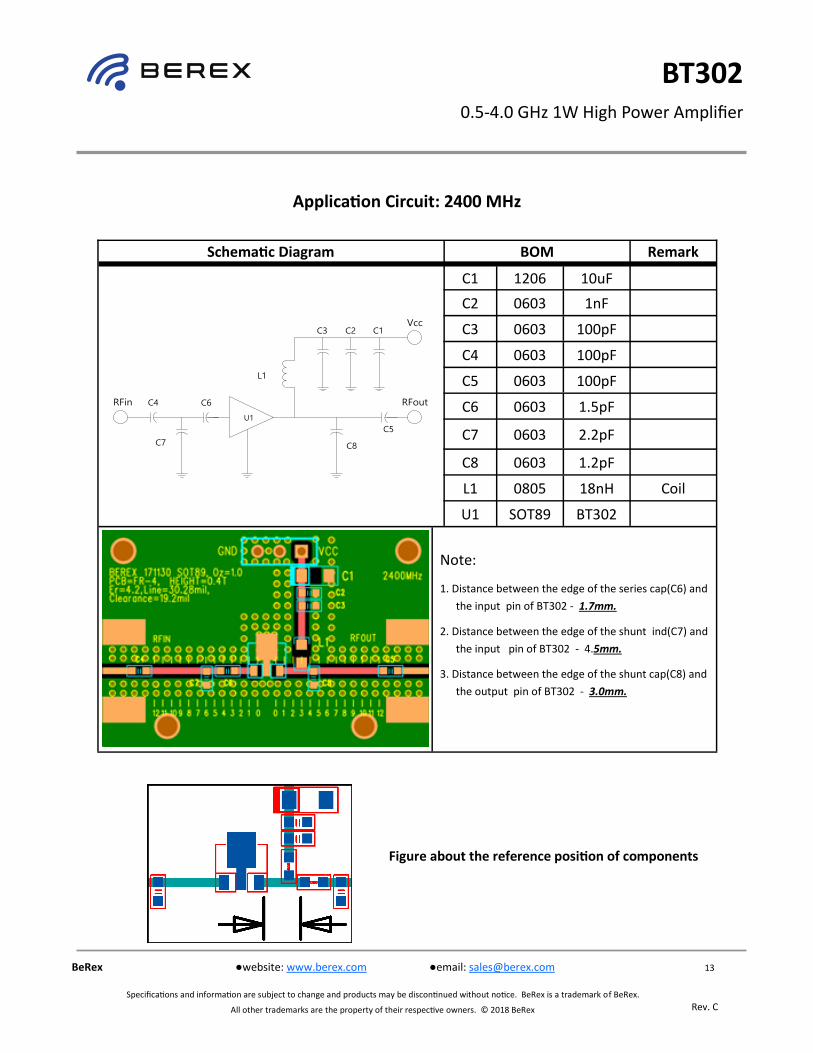
Application Circuit: 2400 MHz
Schematic Diagram BOM Remark
C1 1206 10uF
C2 0603 1nF
C3 0603 100pF
C4 0603 100pF
C5 0603 100pF
C6 0603 1.5pF
C7 0603 2.2pF
C8 0603 1.2pF
L1 0805 18nH Coil
U1 SOT89 BT302
Note:
1. Distance between the edge of the series cap(C6) and
the input pin of BT302 - 1.7mm.
2. Distance between the edge of the shunt ind(C7) and
the input pin of BT302 - 4.5mm.
3. Distance between the edge of the shunt cap(C8) and
the output pin of BT302 - 3.0mm.
Figure about the reference position of components
U1
C4
L1
C3 C2 C1
C5
RFin RFout
Vcc
C8C7
C6

0.5-4.0 GHz 1W High Power Amplifier
BT302
14
Rev. C
BeRex website: www.berex.com email: [email protected]
Specifications and information are subject to change and products may be discontinued without notice. BeRex is a trademark of BeRex.
All other trademarks are the property of their respective owners. © 2018 BeRex
Vc = 5V, Ic = 215mA
Typical Performance
0.5-4.0 GHz 1W High Power Amplifier
BT302
15
Rev. C
BeRex website: www.berex.com email: [email protected]
Specifications and information are subject to change and products may be discontinued without notice. BeRex is a trademark of BeRex.
All other trademarks are the property of their respective owners. © 2018 BeRex
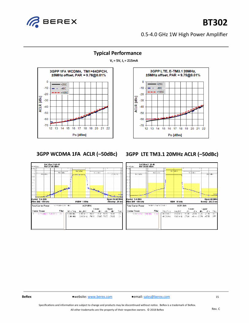
3GPP WCDMA 1FA ACLR (–50dBc) 3GPP LTE TM3.1 20MHz ACLR (–50dBc)
Vc = 5V, Ic = 215mA
Typical Performance
0.5-4.0 GHz 1W High Power Amplifier
BT302
16
Rev. C
BeRex website: www.berex.com email: [email protected]
Specifications and information are subject to change and products may be discontinued without notice. BeRex is a trademark of BeRex.
All other trademarks are the property of their respective owners. © 2018 BeRex
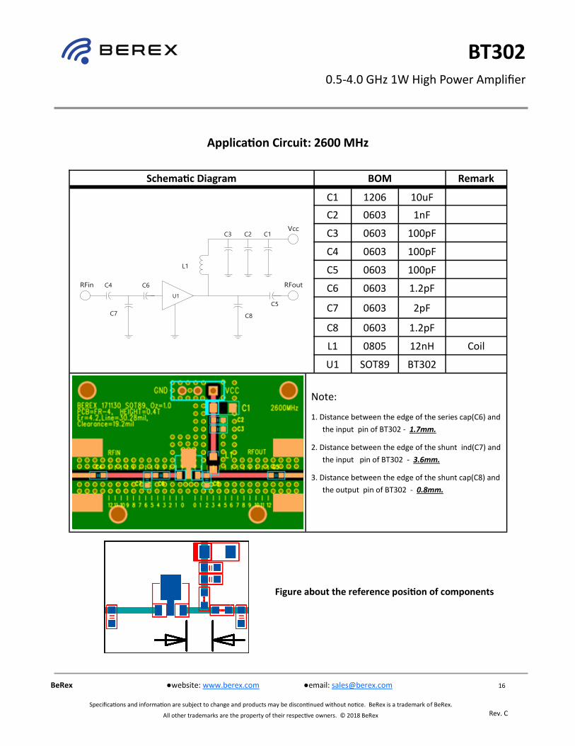
Application Circuit: 2600 MHz
Schematic Diagram BOM Remark
C1 10uF 1206
C2 1nF 0603
C3 100pF 0603
C4 100pF 0603
C5 100pF 0603
C6 1.2pF 0603
C7 2pF 0603
C8 1.2pF 0603
L1 0805 12nH Coil
U1 BT302 SOT89
Note:
1. Distance between the edge of the series cap(C6) and
the input pin of BT302 - 1.7mm.
2. Distance between the edge of the shunt ind(C7) and
the input pin of BT302 - 3.6mm.
3. Distance between the edge of the shunt cap(C8) and
the output pin of BT302 - 0.8mm.
Figure about the reference position of components
U1
C4
L1
C3 C2 C1
C5
RFin RFout
Vcc
C8C7
C6
0.5-4.0 GHz 1W High Power Amplifier
BT302
17
Rev. C
BeRex website: www.berex.com email: [email protected]
Specifications and information are subject to change and products may be discontinued without notice. BeRex is a trademark of BeRex.
All other trademarks are the property of their respective owners. © 2018 BeRex
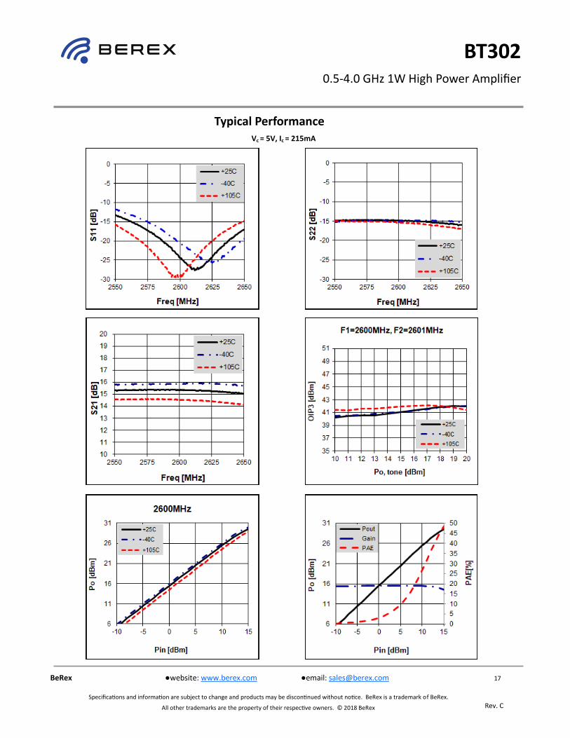
Vc = 5V, Ic = 215mA
Typical Performance

0.5-4.0 GHz 1W High Power Amplifier
BT302
18
Rev. C
BeRex website: www.berex.com email: [email protected]
Specifications and information are subject to change and products may be discontinued without notice. BeRex is a trademark of BeRex.
All other trademarks are the property of their respective owners. © 2018 BeRex
3GPP WCDMA 1FA ACLR (–50dBc) 3GPP LTE TM3.1 20MHz ACLR (–50dBc)
Vc = 5V, Ic = 215mA
Typical Performance

0.5-4.0 GHz 1W High Power Amplifier
BT302
19
Rev. C
BeRex website: www.berex.com email: [email protected]
Specifications and information are subject to change and products may be discontinued without notice. BeRex is a trademark of BeRex.
All other trademarks are the property of their respective owners. © 2018 BeRex
Application Circuit: 3500 MHz
Schematic Diagram BOM Remark
C1 10uF 1206
C2 1nF 0603
C3 100pF 0603
C4 100pF 0603
C5 100pF 0603
C6 0.3pF 0603
C7 0.5pF 0603
C8 0.75pF 0603
L1 0805 18nH Coil
U1 BT302 SOT89
Note:
1. Distance between the edge of the series cap(C6) and
the input pin of BT302 - 1.7mm.
2. Distance between the edge of the shunt cap(C7) and
the input pin of BT302 - 6.7mm.
3. Distance between the edge of the shunt cap(C8) and
the output pin of BT302 - 0.4mm.
Figure about the reference position of components
U1
C4
L1
C3 C2 C1
C5
RFin RFout
Vcc
C8C7
C6

0.5-4.0 GHz 1W High Power Amplifier
BT302
20
Rev. C
BeRex website: www.berex.com email: [email protected]
Specifications and information are subject to change and products may be discontinued without notice. BeRex is a trademark of BeRex.
All other trademarks are the property of their respective owners. © 2018 BeRex
Vc = 5V, Ic = 215mA
Typical Performance

0.5-4.0 GHz 1W High Power Amplifier
BT302
21
Rev. C
BeRex website: www.berex.com email: [email protected]
Specifications and information are subject to change and products may be discontinued without notice. BeRex is a trademark of BeRex.
All other trademarks are the property of their respective owners. © 2018 BeRex
3GPP WCDMA 1FA ACLR (–50dBc) 3GPP LTE TM3.1 20MHz ACLR (–50dBc)
Vc = 5V, Ic = 215mA
Typical Performance
0.5-4.0 GHz 1W High Power Amplifier
BT302
22
Rev. C
BeRex website: www.berex.com email: [email protected]
Specifications and information are subject to change and products may be discontinued without notice. BeRex is a trademark of BeRex.
All other trademarks are the property of their respective owners. © 2018 BeRex
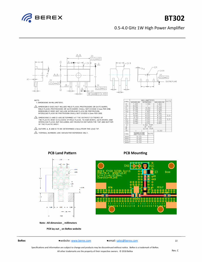
PCB Land Pattern PCB Mounting
Note : All dimension _ millimeters
PCB lay out _ on BeRex website

0.5-4.0 GHz 1W High Power Amplifier
BT302
23
Rev. C
BeRex website: www.berex.com email: [email protected]
Specifications and information are subject to change and products may be discontinued without notice. BeRex is a trademark of BeRex.
All other trademarks are the property of their respective owners. © 2018 BeRex
Lead plating finish
100% Tin Matte finish
(All BeRex products undergoes a 1 hour, 150 degree C, Anneal bake to eliminate thin whisker growth concerns.)
MSL / ESD Rating
ESD Rating:
Value:
Test:
Standard:
MSL Rating:
Standard:
Class 1C
Passes <2000V
Human Body Model (HBM)
JEDEC Standard JESD22-A114B
Level 1 at +265°C convection reflow
JEDEC Standard J-STD-020
NATO CAGE code:
2 N 9 6 F
Tape & Reel
SOT89 Packaging information:
Tape Width (mm): 12
Reel Size (inches): 7
Device Cavity Pitch (mm): 8
Devices Per Reel: 1000
Package Marking
YY = Year, WW = Working Week,
XX = Wafer No.


