System Tests with DC-DC Converters for the CMS Silicon...
5
System Tests with DC-DC Converters for the CMS Silicon Strip Tracker at SLHC K. Klein, L. Feld, R. Jussen, W. Karpinski, J. Merz, J. Sammet for the CMS Tracker Collaboration 1.Physikalisches Institut B, RWTH Aachen University, 52074 Aachen, Germany [email protected] Abstract The delivery of power is considered to be one of the major challenges for the upgrade of the CMS silicon strip tracker for SLHC. The inevitable increase in granularity and complexity of the device is expected to result in a power consumption compa- rable or even higher than the power consumption of todays’ strip tracker. However, the space available for cables will remain the same. In addition, a further increase of the tracker material bud- get due to cables and cooling is considered inacceptable, as the performance of the CMS detector must not be compromised for the upgrade. Novel powering schemes such as serial powering or usage of DC-DC converters have been proposed to solve the problem. To test the second option, substructures of the current CMS silicon strip tracker have been operated for the first time with off-the-shelf DC-DC buck converters as well as with first prototypes of custom-designed DC-DC converters. The tests are described and the results are discussed. I. I NTRODUCTION A. Power Distribution in the CMS Strip Tracker The current CMS silicon strip tracker [1] is built of 15 148 silicon strip modules. The power consumption per module in- cluding the optical conversion is 1.8 or 2.7 W (depending on the module type); the whole strip tracker consumes about 33kW. Groups of 2-12 modules are powered in parallel via roughly 50 m long copper low impedance cables from CAEN power sup- plies that are located on the balconies of the experimental cav- ern. The voltage drop on these long cables leads to a loss of 34kW, i.e. 50% of the total delivered power is lost in the ca- bles. The current power system is described in detail in [2]. The power lost inside the cold volume of the tracker contributes to the total heat load, which has to be removed to ensure that the sensors are kept at temperatures below -10 ◦ C, as required to avoid thermal runaway effects. Power cables and cooling struc- tures increase the material budget of the tracker considerably. The routing and installation of the services has been one of the most complex tasks during tracker commissioning. Currently plans for an upgrade of the CMS strip tracker are developed in view of a potential luminosity upgrade of the LHC, the Super-LHC (SLHC). While the design is still under study, it is obvious that the granularity of the tracker will have to be in- creased, while additional complexity will have to be added; in particular, if the tracker information is to be used in the first level trigger stage. On the other hand it is expected that the front-end electronics will be developed in a smaller feature size process, such as 0.13 μm CMOS. For this process and a sen- sor capacitance of 5 pF (current strip sensor capacitances range from 10-25 pF) a decrease of the front-end power per channel by roughly a factor of 5 was estimated [3], an advantage that is partly canceled by lowering the operating voltage from 2.5 V to 1.2-1.3V. In total, while the power consumption of the upgrade tracker is not precisely known as of today, it is very likely that it will equal or exceed the current power consumption. While an increase of the number or cross-section of cables is not desir- able due to the expected increase of the material budget and the accompanying negative effect on the detector performance, it is even considered practically impossible since the tracker services are buried beneath the services of the electromagnetic calorime- ter, and since the space available in the service channels is al- ready occupied by the current services. B. DC-DC Conversion To deal with the problem, which affects both the ATLAS and CMS trackers, two solutions have been proposed: Serial Power- ing (SP) and powering with DC-DC converters. While in SP a number of modules are connected in series to a constant current source, DC-DC converters [4] are used to convert a high DC input voltage to a lower DC output voltage. In this paper, we concentrate on the latter option. The ratio of the output to the input voltage, V out /V in , is called the conversion ratio, here denoted as r. If r is small, ideally much smaller than 1, the input current can be smaller by the same factor, leading to a reduction of the power loss by r 2 . In a simple approach, one converter could be installed per module. Several technologies exist, but mostly inductors or capacitors are used as energy storage elements. For each tech- nology there is a great variety of topologies and designs. The simplest inductor-based step-down (i.e. r< 1) converter type is the “buck” converter. Its basic circuit consists of a switch, which is typically implemented as two transistors, an inductor for energy storage, and a filter capacitor. Realistic devices fea- ture also a feedback circuit based on Pulse Width Modulation (PWM). DC-DC converters are flexible: with the same basic circuit, various output voltages can be achieved with minor re- configurations, and several converter stages can be combined. In contrast to capacitor-based approaches, inductor-based designs can in general provide currents of several Amperes. Challenges are the achievement of an efficiency as high as possible, the need for a radiation-hard technology that supports the high input volt- age (expected to be around 10 V for SLHC applications), as well as the potential generation of switching noise. Another issue for inductor-based layouts is the requirement to operate in a high
-
Upload
nguyenkhanh -
Category
Documents
-
view
216 -
download
0
Transcript of System Tests with DC-DC Converters for the CMS Silicon...

System Tests with DC-DC Converters for the CMS Silicon Strip Tracker at SLHC
K. Klein, L. Feld, R. Jussen, W. Karpinski, J. Merz, J. Sammet
for the CMS Tracker Collaboration
1. Physikalisches Institut B, RWTH Aachen University, 52074 Aachen, Germany
Abstract
The delivery of power is considered to be one of the majorchallenges for the upgrade of the CMS silicon strip tracker forSLHC. The inevitable increase in granularity and complexity ofthe device is expected to result in a power consumption compa-rable or even higher than the power consumption of todays’ striptracker. However, the space available for cables will remain thesame. In addition, a further increase of the tracker material bud-get due to cables and cooling is considered inacceptable, as theperformance of the CMS detector must not be compromised forthe upgrade. Novel powering schemes such as serial poweringor usage of DC-DC converters have been proposed to solve theproblem. To test the second option, substructures of the currentCMS silicon strip tracker have been operated for the first timewith off-the-shelf DC-DC buck converters as well as with firstprototypes of custom-designed DC-DC converters. The tests aredescribed and the results are discussed.
I. INTRODUCTION
A. Power Distribution in the CMS Strip Tracker
The current CMS silicon strip tracker [1] is built of 15 148silicon strip modules. The power consumption per module in-cluding the optical conversion is 1.8 or 2.7 W (depending on themodule type); the whole strip tracker consumes about 33 kW.Groups of 2-12 modules are powered in parallel via roughly50 m long copper low impedance cables from CAEN power sup-plies that are located on the balconies of the experimental cav-ern. The voltage drop on these long cables leads to a loss of34 kW, i.e. 50% of the total delivered power is lost in the ca-bles. The current power system is described in detail in [2]. Thepower lost inside the cold volume of the tracker contributes tothe total heat load, which has to be removed to ensure that thesensors are kept at temperatures below −10 ◦C, as required toavoid thermal runaway effects. Power cables and cooling struc-tures increase the material budget of the tracker considerably.The routing and installation of the services has been one of themost complex tasks during tracker commissioning.
Currently plans for an upgrade of the CMS strip tracker aredeveloped in view of a potential luminosity upgrade of the LHC,the Super-LHC (SLHC). While the design is still under study, itis obvious that the granularity of the tracker will have to be in-creased, while additional complexity will have to be added; inparticular, if the tracker information is to be used in the firstlevel trigger stage. On the other hand it is expected that thefront-end electronics will be developed in a smaller feature size
process, such as 0.13 µm CMOS. For this process and a sen-sor capacitance of 5 pF (current strip sensor capacitances rangefrom 10-25 pF) a decrease of the front-end power per channelby roughly a factor of 5 was estimated [3], an advantage that ispartly canceled by lowering the operating voltage from 2.5 V to1.2-1.3 V. In total, while the power consumption of the upgradetracker is not precisely known as of today, it is very likely thatit will equal or exceed the current power consumption. Whilean increase of the number or cross-section of cables is not desir-able due to the expected increase of the material budget and theaccompanying negative effect on the detector performance, it iseven considered practically impossible since the tracker servicesare buried beneath the services of the electromagnetic calorime-ter, and since the space available in the service channels is al-ready occupied by the current services.
B. DC-DC Conversion
To deal with the problem, which affects both the ATLAS andCMS trackers, two solutions have been proposed: Serial Power-ing (SP) and powering with DC-DC converters. While in SP anumber of modules are connected in series to a constant currentsource, DC-DC converters [4] are used to convert a high DCinput voltage to a lower DC output voltage. In this paper, weconcentrate on the latter option.
The ratio of the output to the input voltage, Vout/Vin, iscalled the conversion ratio, here denoted as r. If r is small,ideally much smaller than 1, the input current can be smallerby the same factor, leading to a reduction of the power lossby r2. In a simple approach, one converter could be installedper module. Several technologies exist, but mostly inductors orcapacitors are used as energy storage elements. For each tech-nology there is a great variety of topologies and designs. Thesimplest inductor-based step-down (i.e. r < 1) converter typeis the “buck” converter. Its basic circuit consists of a switch,which is typically implemented as two transistors, an inductorfor energy storage, and a filter capacitor. Realistic devices fea-ture also a feedback circuit based on Pulse Width Modulation(PWM). DC-DC converters are flexible: with the same basiccircuit, various output voltages can be achieved with minor re-configurations, and several converter stages can be combined. Incontrast to capacitor-based approaches, inductor-based designscan in general provide currents of several Amperes. Challengesare the achievement of an efficiency as high as possible, the needfor a radiation-hard technology that supports the high input volt-age (expected to be around 10 V for SLHC applications), as wellas the potential generation of switching noise. Another issue forinductor-based layouts is the requirement to operate in a high
magnetic field (4 T for CMS): since ferrite materials saturate,air-core inductors must be used. To achieve the necessary in-ductances, these coils must be relatively large and massive. Dueto the far extension of the magnetic field, the radiation of elec-tromagnetic noise is a potential issue.
To understand better the opportunities and challenges relatedto this proposed solution to the power problem, we have per-formed system test measurements with commercial and customDC-DC converters.
II. THE SYSTEM TEST
A. Set-up Description
In the absence of any prototype structures for the tracker up-grade, substructures of the current tracker end caps, refered toas petals, have been used. While future devices will be differentin many respects, we believe that lessons can be learned fromoperating current tracker structures with DC-DC converters.
The petals as well as the data acquisition chain are describedelsewhere [1]. Here only aspects of the front-end (FE) electron-ics relevant for the system test are described. The test petal wasequipped with four ring-6 modules. This module type carriestwo daisy-chained sensors with AC-coupled p-doped strips im-planted in a 500 µm thick n-doped bulk. The sensor capacitanceamounts to about 20 pF. The connections between sensors andbetween the first sensor and the FE-electronics are realized withwire bonds. The FE-hybrid carries six APV25 readout chips [5],which are manufactured in a 0.25 µm CMOS process. Each chipprocesses the data of 128 channels. The read-out is fully ana-logue. For each channel, a charge-sensitive pre-amplifier, a CR-RC filter with a time constant of 50 ns, and a 192 cells deeppipeline are implemented. The data are sampled at 40 MHz.Two readout modes can be selected: in peak mode only onesample is used per event; in deconvolution mode a weighted sumof three consecutive samples is formed to reduce the effectiveshaping time to 25 ns. On receipt of a level-1 trigger, the dataare output with a rate of 20 MS/s. Data of two APVs are multi-plexed onto one optical channel by the APVMUX chip, result-ing in a 40 MS/s serial output stream. The APV25 is poweredfrom two supply rails, namely 1.25 V and 2.5 V. Typical cur-rents are 60 mA and 120 mA, respectively [2]. All other chipson the hybrid as well as the analog-optical converters (Analog-Opto Hybrids, AOH) and the controller chips (Central ControlUnits, CCU) operate with a supply voltage of 2.5 V.
All modules have been powered and read-out during themeasurements. The petal was equipped with the original moth-erboards (InterConnect Board, ICB), AOHs and CCU modules.Both readout and digital signalling (trigger, clock, fast controls)was realized optically. PCI-based prototypes of the ADC card(Front End Driver), the trigger card (Trigger Sequencer Card)and the controller card (Front End Controller) have been used.The petal has been thermally stabilized at +15 ◦C. It was housedin a grounded metal box. The set-up was very similar to test sys-tems used during integration of the CMS tracker [6].
The modules have been commissioned with a well-knownprocedure and operated with fully depleted sensors, mostly inpeak mode.
B. Analysis Method
The analysis method is described in [6]. The raw or totalnoise is calculated as the RMS of the fluctuations around thepedestal value, which is the mean strip signal without particlestraversing the detector. The common mode (CM) is defined asa common event-wise fluctuation of all strips of an APV, and iscalculated as the median of the signals after subtraction of thepedestals. It is included in the raw noise. The common modenoise is the RMS of the common mode. At least 100 000 eventshave been taken per run to assure stable conditions, of which10 000 events, starting from event 90 000, have been analyzed.
III. MEASUREMENT RESULTS
A. Commercial DC-DC Converters with InternalFerrite Inductors
Since custom radiation-hard DC-DC converters were notavailable when we started our investigations, we used commer-cial buck converters. The first tests were performed with buckconverters with internal coils.
A market survey was performed to identify a device withhigh switching frequency (i.e. small size of passive compo-nents), low conversion ratio, a suitable output voltage rangeand sufficient output current. The Enpirion buck converterEN5312QI [7] was chosen: with dimensions of 5x4x1.1 mm3,a switching frequency of 4 MHz and a maximum current of 1 Ait is appropriate for our application. A disadvantage is the rel-atively low recommended maximal input voltage of 5.5 V. Thedevice implements an internal planar inductor in MEMS tech-nology. Due to the deployment of magnetic cores it is not usablein a strong magnetic field.
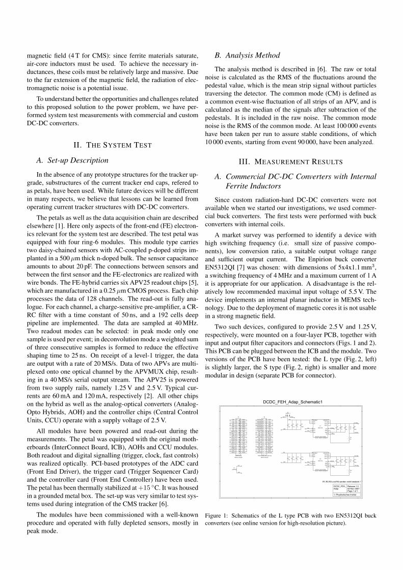
Two such devices, configured to provide 2.5 V and 1.25 V,respectively, were mounted on a four-layer PCB, together withinput and output filter capacitors and connectors (Figs. 1 and 2).This PCB can be plugged between the ICB and the module. Twoversions of the PCB have been tested: the L type (Fig. 2, left)is slightly larger, the S type (Fig. 2, right) is smaller and moremodular in design (separate PCB for connector).
VIN
VSS
IN125EXT
OUT250
VSS
IN250ITHRITH
VSS/RST
SDA
IN250
IN250IN250
IN250IN250
VSSVSS
VSS
VSS
SCLVSS
BCLK+BCLK-
VSS
OUT2+OUT2-
OUT1+
OUT1-
VSS
VSS
VSS
VSS
VSS
OUT0+
OUT0-
OUT250 ITHROUT250
OUT250OUT250
OUT250OUT250OUT125
VSSVSS
VSSOUT125
VSSVSS
OUT125VSS
VSSOUT125
VSS
VSSOUT125
ITH
VSS/RST
SDASCLVSS
BCLK+BCLK-
VSSOUT125
OUT2+OUT2-
OUT125OUT1+
OUT1-OUT125OUT0+
OUT0-OUT125
VFB250
VFB250
VIN
VSS
OUT125
VSSVFB125
VFB125VSS
VIN
VSS
VIN
EXT
VSS
IN125
IN125
IN125
IN125
IN125IN125
IN125
IN125
IN125
U1
EN5312Q
21
16VFB
20 ENABLE
GND
VSENSEVIN
VS0VS1
VS2
GND 3
1
1918
17 4
15
2 VINVOUT 5
VOUT 6
8 9 10 11 12 13 148,9.10,11,12,13,14 NC
7VOUT
TH
X1
NAIS-40-HeaderAXN440330S
40393837
36353433
323130292827
26252423
22212019
18171615
14131211
1098765
4321
X3Jumper_3
21 3
C4
100n
C3
1u
C2
4.7u
C1
22u C7
10u
C6
1u
C5
100n 1kR1
1kR2
100n
C8
U2
EN5312Q
21
16VFB
20 ENABLE
GND
VSENSE
VIN
VS0
VS1VS2
GND 3
1
19
1817 4
15
2 VINVOUT 5
VOUT 6
8 9 10 11 12 13 148,9.10,11,12,13,14 NC
7VOUT
TH
100n
C11
1u
C10
4.7u
C9
10u
C14
1u
C13
100n
C12
1kR3
1kR4
100n
C15
X4JUMPER
NAIS-40-Socket
X2
AXN340038S_ohne_Bohrung
40 3938 37
36 3534 33
32 3130 2928 27
26 2524 23
22 2120 19
18 1716 15
14 1312 11
10 98 76 5
4 32 1
22u
C16
Release 1.005-Nov-2007Page 1 of 1
1. Physikalisches Institut
DCDC_FEH_Adap
R1,R2,R3 und R4 werden nicht bestückt !
DCDC_FEH_Adap_Schematic1
Figure 1: Schematics of the L type PCB with two EN5312QI buckconverters (see online version for high-resolution picture).
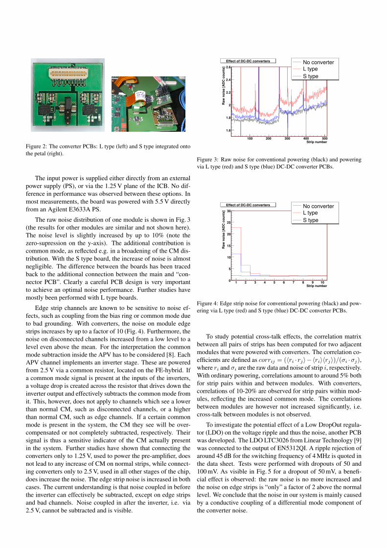
Figure 2: The converter PCBs: L type (left) and S type integrated ontothe petal (right).
The input power is supplied either directly from an externalpower supply (PS), or via the 1.25 V plane of the ICB. No dif-ference in performance was observed between these options. Inmost measurements, the board was powered with 5.5 V directlyfrom an Agilent E3633A PS.
The raw noise distribution of one module is shown in Fig. 3(the results for other modules are similar and not shown here).The noise level is slightly increased by up to 10% (note thezero-supression on the y-axis). The additional contribution iscommon mode, as reflected e.g. in a broadening of the CM dis-tribution. With the S type board, the increase of noise is almostnegligible. The difference between the boards has been tracedback to the additional connection between the main and “con-nector PCB”. Clearly a careful PCB design is very importantto achieve an optimal noise performance. Further studies havemostly been performed with L type boards.
Edge strip channels are known to be sensitive to noise ef-fects, such as coupling from the bias ring or common mode dueto bad grounding. With converters, the noise on module edgestrips increases by up to a factor of 10 (Fig. 4). Furthermore, thenoise on disconnected channels increased from a low level to alevel even above the mean. For the interpretation the commonmode subtraction inside the APV has to be considered [8]. EachAPV channel implements an inverter stage. These are poweredfrom 2.5 V via a common resistor, located on the FE-hybrid. Ifa common mode signal is present at the inputs of the inverters,a voltage drop is created across the resistor that drives down theinverter output and effectively subtracts the common mode fromit. This, however, does not apply to channels which see a lowerthan normal CM, such as disconnected channels, or a higherthan normal CM, such as edge channels. If a certain commonmode is present in the system, the CM they see will be over-compensated or not completely subtracted, respectively. Theirsignal is thus a sensitive indicator of the CM actually presentin the system. Further studies have shown that connecting theconverters only to 1.25 V, used to power the pre-amplifier, doesnot lead to any increase of CM on normal strips, while connect-ing converters only to 2.5 V, used in all other stages of the chip,does increase the noise. The edge strip noise is increased in bothcases. The current understanding is that noise coupled in beforethe inverter can effectively be subtracted, except on edge stripsand bad channels. Noise coupled in after the inverter, i.e. via2.5 V, cannot be subtracted and is visible.
Strip number100 200 300 400 500
Raw
noi
se [A
DC c
ount
s]
1.6
1.8
2
2.2
2.4
2.6Effect of DC-DC converters No converter
L type S type
Figure 3: Raw noise for conventional powering (black) and poweringvia L type (red) and S type (blue) DC-DC converter PCBs.
Strip number1 2 3 4 5 6 7 8 9 10
Raw
noi
se [A
DC c
ount
s]
0
5
10
15
20
25
30Effect of DC-DC converters No converter
L type S type
Figure 4: Edge strip noise for conventional powering (black) and pow-ering via L type (red) and S type (blue) DC-DC converter PCBs.
To study potential cross-talk effects, the correlation matrixbetween all pairs of strips has been computed for two adjacentmodules that were powered with converters. The correlation co-efficients are defined as corrij = (〈ri ·rj〉−〈ri〉〈rj〉)/(σi ·σj),where ri and σi are the raw data and noise of strip i, respectively.With ordinary powering, correlations amount to around 5% bothfor strip pairs within and between modules. With converters,correlations of 10-20% are observed for strip pairs within mod-ules, reflecting the increased common mode. The correlationsbetween modules are however not increased significantly, i.e.cross-talk between modules is not observed.
To investigate the potential effect of a Low DropOut regula-tor (LDO) on the voltage ripple and thus the noise, another PCBwas developed. The LDO LTC3026 from Linear Technology [9]was connected to the output of EN5312QI. A ripple rejection ofaround 45 dB for the switching frequency of 4 MHz is quoted inthe data sheet. Tests were performed with dropouts of 50 and100 mV. As visible in Fig. 5 for a dropout of 50 mV, a benefi-cial effect is observed: the raw noise is no more increased andthe noise on edge strips is “only” a factor of 2 above the normallevel. We conclude that the noise in our system is mainly causedby a conductive coupling of a differential mode component ofthe converter noise.

Strip number100 200 300 400 500
Raw
noi
se [A
DC c
ount
s]
1.6
1.8
2
2.2
2.4
2.6Effect of LDO with internal inductor No converter
Without LDO With LDO
Figure 5: Raw noise for conventional powering (black) and poweringwith a L type PCB with (blue) and without (red) LDO.
B. Commercial DC-DC Converters with ExternalAir-Core Inductors
Since ferrite inductors cannot be used in the final exper-iment, commercial buck converters have been equipped withexternal air-core inductors. For these tests, the Enpirion buckconverter EQ5382D has been chosen, which is similar toEN5312QI, but has no internal inductor. PCBs similar to the Ltype have been fabricated and equipped with various coils: pla-nar ferrite inductors (Murata LQH32CN1R0M23, L = 1 µH),air-core solenoids (Coilcraft 132-20SMJLB, L = 538 nH) andcustom-made air-core toroids (L ≈ 600 nH). With air-core in-ductors, the noise increases drastically compared to internal orexternal ferrite inductors (Fig. 6). For toroids the increase is afactor of 2-3 lower than with solenoids. The edge strip noise in-creases enormously, up to about 90 ADC counts. When a mod-ule was operated with an air-core coil, the noise increased alsoon its conventionally powered neighbour modules.
The wing-shaped noise has been traced to a pick-up of ra-diated noise in the FE-hybrid region. This has been proven intests where the module was powered conventionally but exposedto the radiation of noise by powered but unplugged converterboards or individual coils operated with a frequency generator.In both cases, wing-shaped noise was induced in the module.In one test the PCB was placed above the conventionally pow-ered module and the position of the converter board was variedsystematically. For each position the mean module noise wascomputed. The biggest effect was observed when the PCB wasplaced above the FE-hybrid, while the effect was very smallwhen the board was located above the sensor. With air-corecoils the conductively generated noise is increased as well, pre-sumably by noise coupling from the coil into the PCB itself.Further studies are needed to understand the details of the cou-pling mechanisms and the shapes of the distributions. As ex-pected, using a LDO does decrease the conductive part, but notthe wings (Fig. 6).
Tests have been performed with shielded converters. ThePCB was wrapped in copper or aluminium foil of 35 and30 µm thickness, respectively. The noise decreased significantly(Fig. 7). Grounding the shield did not improve the situation. Nofurther improvement was obtained with thicker shields.
Strip number100 200 300 400 500
Raw
noi
se [A
DC c
ount
s]
0
2
4
6
8
10
Effect of different inductors No converterInternal inductorExt. ferrite inductorExt. air-core inductorExt. air-core inductor, LDO
Figure 6: Raw noise for conventional powering (black) and poweringwith a L type PCB with internal coil (blue), external ferrite coil (red)and external air-core solenoid without (pink) and with (green) LDO.
Strip number100 200 300 400 500
Raw
noi
se [A
DC c
ount
s]
0
2
4
6
8
10
Effect of shielding No converterNo shielding
m aluminiumµ30 m copperµ35
Figure 7: Raw noise for conventional powering (black) and poweringwith a L type PCB with external air-core solenoid, without shielding(red) and with 35 µm copper (green) or 30µm aluminium shielding(blue).
The chosen foils might already be thicker than necessary andthinner shields should be tried. The noise contribution remain-ing with shielding is probably induced conductively. Whileshielding is in general not desirable due to the associated ma-terial, adding an aluminium box of (3 cm)3 (a very conservativeassumption) and a thickness of 30 µm for instance to each mod-ule in the end caps would increase their mass by only 1.5 kg(2 per mille).
Finally the distance between the converter PCB and the FE-hybrid has been varied. For this test, the L type board withexternal air-core solenoids has been equipped with an S typeconnector. A cable has been plugged between the board andthe “connector PCB”, so that distance and cable length couldbe varied. The noise effect depends strongly on the distance.When the distance is increased by a few centimetres, the in-crease of noise is almost negligible. It should be noted that theconductive noise is decreased as well due to passive filtering inthe connector and cable. While space around single modules isexpected to be very constraint in a new tracker, an operation ofbuck converters on the substructure level could thus be feasible.
C. Custom DC-DC Converters
1. The SWREG2 Buck PWM Controller (CERN)
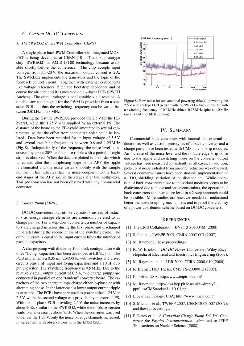
A single phase buck PWM Controller with Integrated MOS-FET is being developed at CERN [10]. The first prototypechip (SWREG2) in AMIS I3T80 technology became avail-able shortly before the conference. The chip accepts inputvoltages from 3.3-20 V; the maximum output current is 2 A.The SWREG2 implements the transistors and the logic of thefeedback control circuit. Together with external componentslike voltage references, filter and bootstrap capacitors and ofcourse the air-core coil it is mounted on a 4-layer PCB (RWTHAachen). The output voltage is configurable via a resistor. Atunable saw-tooth signal for the PWM is provided from a sep-arate PCB and thus the switching frequency can be varied be-tween 250 kHz and 3 MHz.
During the test the SWREG2 provided the 2.5 V for the FE-hybrid, while the 1.25 V was supplied by an external PS. Thedistance of the board to the FE-hybrid amounted to several cen-timetres, so that the effect from conductive noise could be iso-lated. Data have been recorded for an input voltage of 5.5 Vand several switching frequencies between 0.6 and 1.25 MHz(Fig. 8). Independently of the frequency, the noise level is in-creased by about 20%, and a noise ripple with a period of eightstrips is observed. When the data are plotted in the order whichis realized after the multiplexing stage of the APV, the rippleis eliminated and the noise varies smoothly with the samplenumber. This indicates that the noise couples into the back-end stages of the APV, i.e. in the stages after the multiplexer.This phenomenon has not been observed with any commercialconverter.
2. Charge Pump (LBNL)
DC-DC converters that utilize capacitors instead of induc-tors as energy storage elements are commonly refered to ascharge pumps. For a step-down converter, a number of capaci-tors are charged in series during the first phase and dischargedin parallel during the second phase of the switching cycle. Theoutput current is equal to the input current times the number ofparallel capacitors.
A charge pump with divide-by-four stack configuration withthree “flying” capacitors has been developed at LBNL [11]. ThePCB implements a 0.35 µm CMOS IC with switches and drivercircuits plus 1 µF input and flying capacitors and a 10 µF out-put capacitor. The switching frequency is 0.5 MHz. Due to therelatively small output current of 0.5 A, two charge pumps areconnected in parallel on one “tandem” converter board. The ca-pacitors of the two charge pumps charge either in-phase or withalternating phase. In the latter case, a lower output current rippleis expected. The PCBs have been used to power either 1.25 V or2.5 V, while the second voltage was provided by an external PS.With the alt-phase PCB providing 2.5 V, the noise increases byabout 20%, similar to the SWREG2, while the in-phase versionleads to an increase by about 75%. When the converter was usedto deliver the 1.25 V, only the noise on edge channels increased,in agreement with observations with the EN5312QI.
Strip number100 200 300 400 500
Raw
noi
se [A
DC c
ount
s]
1.6
1.8
2
2.2
2.4
2.6
2.8
3
3.2
3.4
SWREG2 frequency scan No converter2.5V from S60.60 MHz0.75 MHz1.00 MHz1.25 MHz
Figure 8: Raw noise for conventional powering (black), powering the2.5 V with a S type PCB (red) or with the SWREG2 buck converter witha switching frequency of 0.6 MHz (blue), 0.75 MHz (pink), 1.0 MHz(green) and 1.25 MHz (brown).
IV. SUMMARY
Commercial buck converters with internal and external in-ductors as well as custom prototypes of a buck converter and acharge pump have been tested with CMS silicon strip modules.An increase of the noise level and the module edge strip noisedue to the ripple and switching noise on the converter outputvoltage has been measured consistently in all cases. In addition,pick-up of noise radiated from air-core inductors was observed.Several countermeasures have been studied: implementation ofa LDO, shielding, variation of the distance etc. While opera-tion of buck converters close to individual modules seems to bedisfavoured due to noise and space constraints, the operation ofbuck converters at substructure level in a 2-step approach couldbe possible. More studies are however needed to understandbetter the noise coupling mechanisms and to proof the viabilityof a power distribution scheme based on DC-DC converters.
REFERENCES
[1] The CMS Collaboration, JINST 3 S08004M (2008).
[2] S. Paoletti, TWEPP 2007, CERN-2007-007 (2007).
[3] M. Raymond, these proceedings.
[4] R. W. Erickson, DC-DC Power Converters, Wiley Ency-clopedia of Electrical and Electronics Engineering (2007).
[5] M. Raymond et al., LEB 2000, CERN-2000-010 (2000).
[6] R. Bremer, PhD Thesis, CMS TS-2008/012 (2008).
[7] Enpirion, USA; http://www.enpirion.com/
[8] M. Raymond, http://icva.hep.ph.ic.ac.uk/∼dmray/ ...pptfiles/CMStracker31 10 01.ppt .
[9] Linear Technology, USA; http://www.linear.com/
[10] S. Michelis et al., TWEPP 2007, CERN-2007-007 (2007);and these proceedings.
[11] P. Denes et al., A Capacitor Charge Pump DC-DC Con-verter for Physics Instrumentation, submitted to IEEETransactions on Nuclear Science (2008).