System Level Modeling and Circuit Design for Low Voltage ...System Level Modeling and Circuit Design...
81
San Jose State University SJSU ScholarWorks Master's eses Master's eses and Graduate Research Spring 2013 System Level Modeling and Circuit Design for Low Voltage CMOS Equalizer for Coaxial Cable for Video Application Han Zhang San Jose State University Follow this and additional works at: hp://scholarworks.sjsu.edu/etd_theses is esis is brought to you for free and open access by the Master's eses and Graduate Research at SJSU ScholarWorks. It has been accepted for inclusion in Master's eses by an authorized administrator of SJSU ScholarWorks. For more information, please contact [email protected]. Recommended Citation Zhang, Han, "System Level Modeling and Circuit Design for Low Voltage CMOS Equalizer for Coaxial Cable for Video Application" (2013). Master's eses. 4325. hp://scholarworks.sjsu.edu/etd_theses/4325
Transcript of System Level Modeling and Circuit Design for Low Voltage ...System Level Modeling and Circuit Design...

San Jose State UniversitySJSU ScholarWorks
Master's Theses Master's Theses and Graduate Research
Spring 2013
System Level Modeling and Circuit Design for LowVoltage CMOS Equalizer for Coaxial Cable forVideo ApplicationHan ZhangSan Jose State University
Follow this and additional works at: http://scholarworks.sjsu.edu/etd_theses
This Thesis is brought to you for free and open access by the Master's Theses and Graduate Research at SJSU ScholarWorks. It has been accepted forinclusion in Master's Theses by an authorized administrator of SJSU ScholarWorks. For more information, please contact [email protected].
Recommended CitationZhang, Han, "System Level Modeling and Circuit Design for Low Voltage CMOS Equalizer for Coaxial Cable for Video Application"(2013). Master's Theses. 4325.http://scholarworks.sjsu.edu/etd_theses/4325
SYSTEM-LEVEL MODELING AND CIRCUIT DESIGN FOR LOW
VOLTAGE CMOS EQUALIZER FOR COAXIAL CABLE FOR VIDEO
APPLICATION
A Thesis
Presented to
The Faculty of the Department of Electrical Engineering
San José State University
In Partial Fulfillment
of the Requirements for the Degree
Master of Science
by
Han Zhang
May 2013

© 2013
Han Zhang
ALL RIGHT RESERVED

The Designated Thesis Committee Approves the Thesis Titled
SYSTEM-LEVEL MODELING AND CIRCUIT DESIGN FOR LOW
VOLTAGE CMOS EQUALIZER FOR COAXIAL CABLE FOR VIDEO
APPLICATION
by
Han Zhang
APPROVED FOR THE DEPARTMENT OF ELECTRICAL ENGINEERING
SAN JOSÉ STATE UNIVERSITY
May 2013
Dr. Shahab Ardalan Department of Electrical Engineering
Dr. Sotoudeh Hamedi-Hagh Department of Electrical Engineering
Prof. Morris Jones Department of Electrical Engineering
ABSTRACT
SYSTEM-LEVEL MODELING AND CIRCUIT DESIGN FOR LOW
VOLTAGE CMOS EQUALIZER FOR COAXIAL CABLE FOR VIDEO
APPLICATION
by Han Zhang
A new method of modeling coaxial cable frequency response with genetic
algorithm was introduced. A system-level multi-stages adaptive equalizer model with
QFB block was generated and tested with multiple cable models, pathological
PRBS-23 data with data rate 1.5 GHz was used. This thesis also provided analysis of
influences on output by using different parameters in simulations. Two adaptive
equalizer circuits with different pre-amplifiers were implemented in GPDK 45 nm
CMOS technology. Related simulations about adaptive ability, single stage
compensation ability, and cascade stages compensation ability were completed. A
tradeoff between output eye height and peak-to-peak jitter was discussed based on
different simulations. Future work will be digital control circuit implementation,
entire circuit fabrication, and testing.

v
ACKNOWLEDGEMENTS
I would like to express my deepest gratitude to my advisor Dr. Shahab Ardalan for
his patient guidance and fully support throughout the entire work. Thank you for
opening the door of mix signal design and being the constant source of inspiration for
me during my master study.
I would also like to thank other members on my thesis committee, Dr. Sotoudeh
Hamedi-Hagh and Prof. Morris Jones. Their participation has provided me valuable
advises in my research.
Great thanks to my lab mates, Yu Feng, Zain and Alfred. Thanks for all your help.
It has been fun working with you guys.
Finally, I am grateful for the support from my parents, my wife Yue Zhao, and my
son Kyle Zhang. Thank you for standing beside me all these years and I love you all.
vi
Table of Contents
Chapter 1. Introduction ............................................................................................ 1
1.1 Coaxial Cable Characteristics .......................................................................... 1
1.2 Equalizer ............................................................................................................ 3
1.3 Equalizer Market Overview ............................................................................... 6
1.4 Motivation and Outline ...................................................................................... 7
Chapter 2. Equalizer System-level Modeling .......................................................... 8
2.1 Cable and Equalizer Model ................................................................................ 8
2.1.1 Genetic Algorithm ....................................................................................... 8
2.1.2 Cable Model Optimization using Genetic Algorithm ............................... 11
2.1.3 Equalizer Model ........................................................................................ 17
2.2 Adaptive Equalization ...................................................................................... 19
2.3 Quantization Feedback (QFB) Block ............................................................... 24
2.3.1 Zero-Wander Effect ................................................................................... 24
2.3.2 Quantization Feedback Modeling ............................................................. 26
2.4 Adaptive Equalizer Model with QFB Block .................................................... 29
Chapter 3. Circuit Implementation ....................................................................... 37
3.1 Methodology .................................................................................................... 37
3.2 Differential Amplifier ...................................................................................... 40
3.3 Wide Swing Current Mirror and Folded Cascode ........................................... 43
3.4 Gilbert Cell and Folded Gilbert Cell ................................................................ 49
3.5 RC Degeneration .............................................................................................. 51
3.6 Folded Cascode Amplifier Type Equalizer Stage ............................................ 53
3.7 Differential Amplifier Type Equalizer Stage ................................................... 55
3.8 Adaptive Simulation Results and Cascade Simulation Results ....................... 57
Chapter 4. Conclusion and Future Work.............................................................. 63
vii
References ................................................................................................................... 65
Appendix ..................................................................................................................... 67
1. Model of A Single Adaptive Equalizer Stage ...................................................... 67
2. CMOS Folded Cascode Amplifier in GPDK 45 nm Technology ........................ 68
3. Folded Cascode Amplifier Type Equalizer Stage ................................................ 69
4. Differential Amplifier Type Equalizer Stage ....................................................... 70

viii
List of Figures
Figure 1.1 : A Common Coaxial Cable ......................................................................... 1
Figure 1.2 : Belden 1694A Coaxial Cable Attenuation for Different Cable Lengths .... 2
Figure 1.3 : Coaxial Cable Output Eye-diagram and Expected Equalized Output ........ 3
Figure 1.4 : Ideal Equalization Process.......................................................................... 4
Figure 1.5 : Eye Diagram Measurements. ..................................................................... 5
Figure 2.1 : Evolution Process in Genetic Algorithm .................................................. 10
Figure 2.2 : Initialization Process of Zero-Pole Vector ............................................... 13
Figure 2.3 : Crossover Process..................................................................................... 15
Figure 2.4 : Fitness Function Value over Generations ................................................ 16
Figure 2.5 : 60 m Belden 1694A Coaxial Cable Model Results .................................. 17
Figure 2.6 : 60 m Belden 1694A Coaxial Cable Equalizer Model .............................. 18
Figure 2.7 : Adaptive Equalizer Model with Different Alpha Values ......................... 20
Figure 2.8 : Automatic Gain Control Model ................................................................ 21
Figure 2.9 : Model of A Single Adaptive Equalizer Stage .......................................... 22
Figure 2.10 : Input and Output of Adaptive Equalizer Model ..................................... 24
Figure 2.11 : Pathological Data Combined with PRBS-23 Data Zero-Wander Effect 25
Figure 2.12 : QFB Block Illustration ........................................................................... 26
Figure 2.13 : Typical QFB Simulink Model ................................................................ 27
Figure 2.14 : QFB Output Results ............................................................................... 28
Figure 2.15 : Complete Equalizer System Model ........................................................ 29
Figure 2.16 : 120 m Belden 1694A Coaxial Cable Equalization Results .................... 31
Figure 2.17 : 40 m Belden 1694A Coaxial Cable Equalization Results ...................... 33
Figure 2.18 : 200 m Belden 1694A Coaxial Cable Equalization Results .................... 34
Figure 2.19 : 240 m Belden 1694A Coaxial Cable Equalization Results .................... 36
Figure 2.20 : 20 m Belden 1694A Coaxial Cable Equalization Results ...................... 37
Figure 3.1 : Design Flow of Equalizer ......................................................................... 39
ix
Figure 3.2 : CMOS Differential Amplifier in GPDK 45 nm Technology ................... 41
Figure 3.3 : Frequency Response of the Differential Amplifier .................................. 43
Figure 3.4 : Wide Swing Current Mirror ..................................................................... 44
Figure 3.5 : Folded Cascode Amplifier........................................................................ 45
Figure 3.6 : CMOS Folded Cascode Amplifier in GPDK 45 nm Technology ............ 47
Figure 3.7 : Frequency Response of the Folded Cascode Amplifier ........................... 48
Figure 3.8 : Gilbert Cell ............................................................................................... 49
Figure 3.9 : CMOS Folded Gilbert Cell in GPDK 45 nm Technology ....................... 50
Figure 3.10 : Folded Gilbert Tuning Results ............................................................... 51
Figure 3.11 : RC Degeneration .................................................................................... 52
Figure 3.12 : Folded Cascode Amplifier Type Equalizer Stage .................................. 54
Figure 3.13 : Differential Amplifier Type Equalizer Stage ......................................... 56
Figure 3.14 : Differential Amplifier Type Equalizer Stage Adaptive Output ............. 58
Figure 3.15 : Differential Amplifier Type Equalizer Stage Cascade Results .............. 60
Figure 3.16 : Folded Cascode Amplifier Type Equalizer Stage Cascade Results ....... 62

x
List of Tables
Table 1. Specifications of Equalizers from Different Companies..................................6
Table 2. Transistor Sizes and Devices Parameters of 45 nm Differential Amplifier....42
Table 3. Transistor Sizes in Folded Cascode and Wide Swing Current Mirror............47
Table 4. Target Frequency Response for 80 m Belden 1694A Coaxial Cable...............53
Table 5. Targeting Frequency Response and Circuit Frequency Response of Differential
Amplifier Equalizer Stages.............................................................................58
Table 6. Targeting Frequency Response and Circuit Frequency Response of Folded
Cascode Amplifier Equalizer Stages..............................................................61

1
Chapter 1. Introduction
1.1 Coaxial Cable Characteristics
Coaxial cables are normally composed of four layers, from inside to outside, there
is an inner conductor core, an inner dielectric insulator layer, a conducting shield layer,
and an insulating outer jacket.
Figure 1.1: A Common Coaxial Cable
Coaxial cables are commonly used as transmission lines for radio, video,
measurement, and data signals. Due to the DC resistance of the center conductor and
dissipation factor of the dielectric material [1], one typical characteristic of the coaxial
cables is cable loss. This can be modeled as a function of signal frequency and cable
length [2]:
𝐶 𝑓, 𝑙 = 𝑒−𝑘𝑠𝑙 1+𝑗 𝑓−𝑘𝑑 𝑙𝑓 (1.1)
where 𝑘𝑠and 𝑘𝑑 are the cable constants, 𝑓 is signal frequency, and 𝑙 is the cable
2
length. According to Eq. (1.1), cable loss increases while cable length increases or
signal frequency increases. A Belden 1694A coaxial cable was used to generate the
relationship between cable loss, signal frequency, and cable length. This relationship
is shown in Figure 1.2.
Figure 1.2: Belden 1694A Coaxial Cable Attenuation for Different Cable Lengths
If an 80 m 1694A coaxial cable were used to transmit a 1080P full HD video signal
with a data rate 1.5 Gbps, the cable loss will be 20 dB. This loss greatly limits the use
of the coaxial cable.

3
1.2 Equalizer
Cable loss directly causes vertical distortion in the eye diagram and horizontal
distortion in the form of jitter [3]. A direct view of these effects and the necessity for
equalizers are shown in Figure 1.3 below.
Figure 1.3: Coaxial Cable Output Eye-diagram and Expected Equalized Output
In order to compensate for the cable loss, an equalizer is used. Due to the
low-pass characteristics of the cable in frequency domain, an ideal equalizer should
have the opposite frequency response, allowing the combined frequency response to be
an all-pass [4].
The theoretical transfer function of an equalizer is given by:
1
,,
E f lC f l
(1.2)
where 𝐶 𝑓, 𝑙 is the cable loss in terms of frequency and length.
In practice, analog equalizers are designed with a transfer function 𝐸 𝑓, 𝑙 in the
frequency range from 0 Hz to the signal frequency. High frequency components in the
4
signal are amplified whereas low frequency components remain the same. Frequency
components higher than the signal frequency should be attenuated to limit high
frequency noise.
An ideal equalization process for a 1 GHz signal is shown in Figure 1.4. After
equalization, the frequency response from 0 Hz to 1 GHz has an all-pass characteristic,
and displays a low-pass response after 1GHz.
(a)
(b)
Figure 1.4: Ideal Equalization Process (a) Cable and Equalizer Frequency Response
(b) Combined Frequency Response.

5
In the output eye diagram, peak-to-peak jitter and eye height are commonly used
as metrics to determine equalizer functionality and performance. Maximum eye
height and minimum peak-to-peak jitter is the goal of equalizer design. Eye height is
measured in volts. Peak-to-peak jitter is usually represented by a proportion of an unit
interval (UI), which quantifies the jitter in terms of a fraction of the ideal bit period [5].
The eye height, peak-to-peak jitter, and UI are shown in Figure 1.5.
Figure 1.5: Eye Diagram Measurements.
Output eye diagrams from well-designed equalizers should have eye heights close
to the original signal, and the peak-to-peak jitter should be less than 0.2 UI. The jitter
requirement is strict because a clock and data recovery circuit will be used after the
equalizer.

6
1.3 Equalizer Market Overview
In today's market, most of the coaxial cable equalizers are implemented with
Bipolar Junction Transistors (BJT). Table 1 compares six recent products from three
major companies.
Table 1. Specifications of Equalizers from Different Companies
Products Data Rates Supply
Voltage Power Jitter
Latest
Update
DS15EA101
(National Semi)
150 Mbps
To
1.5+ Gbps
Single
3.3V
210 mW
at 1.5
Gbps
0.25 UI
to
0.4 UI
Jan. 2012
DS30EA101
(National Semi)
150 Mbps
To
3.125 Gbps
Single
2.5V
115 mW
Typical
0.2 UI
to
0.35 UI
Feb. 2012
M21424
(Mindspeed)
143 Mbps
to
2970 Mbps
2.5V
or
3.3V
175 mW
to
312 mW
0.2 UI
to
0.35 UI
Mar. 2010
GS3441
(Semtech)
270 Mbps
to
2.97 Gbps
Single
3.3V
237 mW
Typical n/a Jan. 2010
GS3440
(Semtech)
270 Mbps
to
2.97 Gbps
Single
3.3V
175 mW
Typical n/a
Aug.
2011
GS2984
(Semtech)
270 Mbps
to
2.97 Gbps
Single
3.3V
195 mW
Typical
0.2 UI
to
0.3 UI
Mar. 2010
7
All of these coaxial cable equalizers are implemented with BJTs, and their supply
voltage varies from 2.5 V to 3.3 V. All designs are adaptive to different data rates and
cable lengths.
1.4 Motivation and Outline
Present-day supply voltages of digital circuits are scaling with reductions in
transistor channel lengths. The supply voltage for a 45 nm complementary
metal-oxide semiconductor (CMOS) process is 1 V. The equalizer interfaces between
the analog transmission line and the digital circuit, so implementing designs in CMOS
is advantageous. When the supply voltages of the equalizer and digital circuits are
compatible, the receiver system does not require separate power supplies. CMOS
design also allows for better portability across processes.
In this thesis, a system-level adaptive coaxial cable equalizer with automatic gain
control (AGC) function and quantization feedback (QFB) block was modeled in
Simulink. Using a Belden 1694A coaxial cable as the transmission line, the equalizer
model was able to adaptively compensate for the cable loss for different cable lengths.
The maximum cable length it can compensate for was 240 m. Circuits were then
designed and simulated using GPDK 45 nm CMOS technology. This work aimed for
applications with a full HD 1080P video signal, so a 1.5 GHz PRBS-23 data with
pathologic patterns stream was used in both modeling and circuit design.
8
Chapter 2. Equalizer System-level Modeling
2.1 Cable and Equalizer Model
The genetic algorithm is an evolutionary algorithm in inartificial intelligence filed
and commonly used for optimization problems. It is used for problems without clear
mathematic expressions. It is usually used in a continuous system or at least in a
system with continuous-like performance.
2.1.1 Genetic Algorithm
Several concepts need to be introduced before starting the algorithm. A candidate
solution is referred to as a chromosome and a group of them is called a population or a
generation. The number of chromosomes in a population should be selected based on
the application. Larger population reduces the number of generations needed to finish
the evolution while requiring an increase in calculation time for each generation. A
fitness function is used to evaluate the optimization fitness of every chromosome in the
population. Fitness functions should be well chosen since final solutions are selected
through a fitness-based process. Evolution is defined as the process that generates a
new population from the existing population.
A typical genetic algorithm starts with an initialization process, where the initial
population is randomly generated in an area where optimal solutions are likely to be
found based on a reasonable prediction.

9
To end the evolution process, a termination condition should be defined such as
finding a solution satisfying minimum criterion. In the case where no improvement is
made after some number of generations, parameters can be modified and resume the
evolution process to seek fitter solutions.
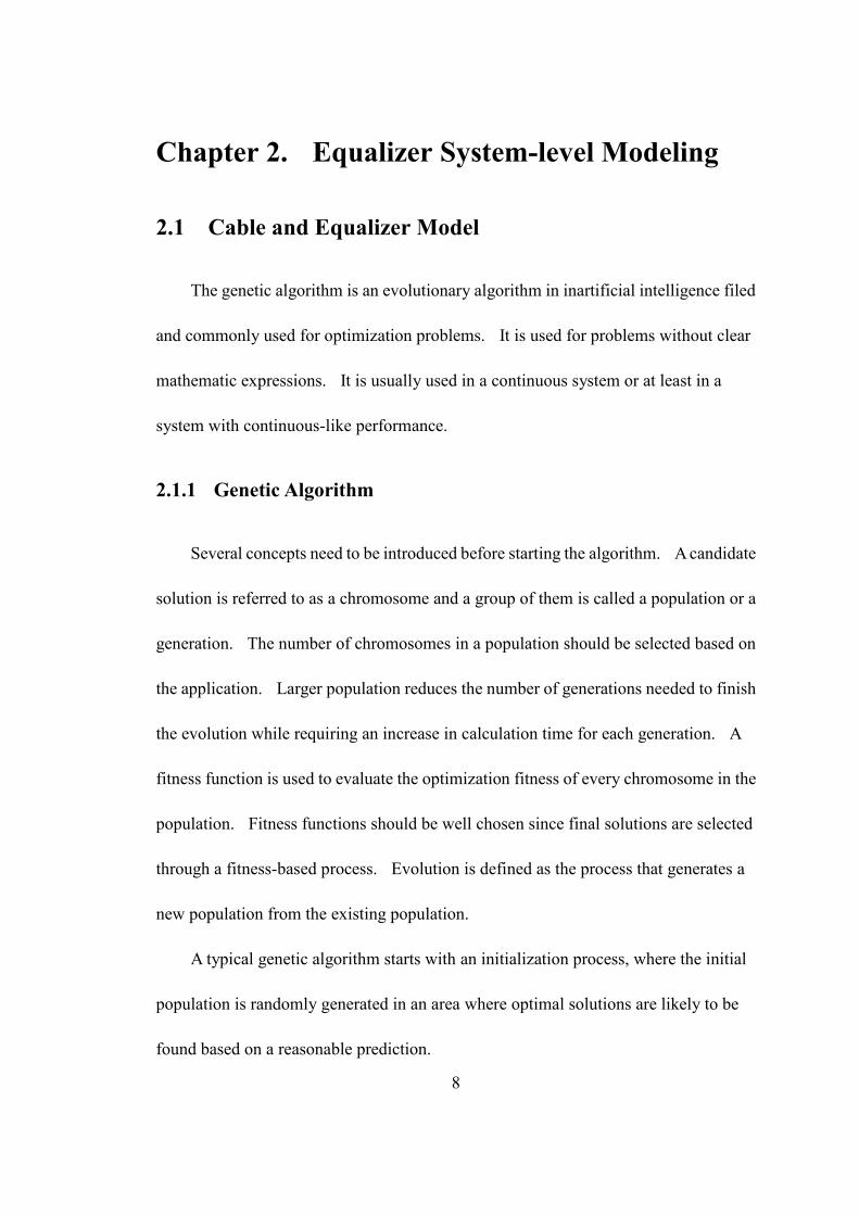
The evolution process, as the key process of the genetic algorithm, is illustrated in
Figure 2.1. After evaluating all the chromosomes with the fitness function, if a
terminal condition is not reached, the chromosomes are divided into three groups:
fittest chromosome group, normal chromosome group, and least fit chromosome group.
The fittest group and the least fit group should take up only a small proportion of the
entire population. This division is the selection process.
The least fit chromosome group is removed from the population because it has the
worst results. Crossover or recombination process is provided to the fittest
chromosome group for generating new solutions, which helps to maintain a certain
number of chromosomes in the population and raises the probability of generating fitter
solutions. A pair of parent solutions is used to produce a child solution or a pair of
children solutions. In the pair of children solutions, one child shares some
components from each parent, and the other child has the remainder. The crossover
process continues until a new population of appropriate size is generated.
10
Figure 2.1: Evolution Process in Genetic Algorithm
A mutation process is provided to the normal chromosome group, since
chromosomes in this group have potential to become either more or less fit. All
characteristics of the chromosomes in the normal chromosome group mutate at a proper
mutation rate based on a given mutation probability. Mutation process replaces a part
of the chromosomes, but it does not change the population size. Mutation rate and
mutation probability should be chosen carefully. A high mutation rate causes large
variations between new and old chromosomes, which lower the probability of finding
fitter solutions. However, low mutation rate slows down the overall speed of
convergence to fitter solutions. Mutation probability value has less effect than
mutation rate [6].
After the selection, crossover, and mutation processes, a new population is
generated. Since the least fit group has been removed, the fittest group has been kept
and enlarged by the crossover process, and normal group has been mutated, there is a
11
higher probability for the new population to meet the termination condition. While
progressing from generation to generation, the terminal condition will be met
eventually or the evolution will stop at a certain level. Outside stimulus is required to
continue the evolution after this point.
The genetic algorithm is commonly used for single object optimization. The
complexity of the genetic algorithm facing multiple objects increases significantly with
the number of objects, especially when the objects are dependent on each other. In this
thesis, the genetic algorithm was used to optimize the cable system function.
2.1.2 Cable Model Optimization using Genetic Algorithm
Cable characteristics versus cable length and signal frequency can be obtained
from the Belden 1694A coaxial cable data sheet. To model the cable, a transfer
function was generated with similar frequency response characteristics in a proper
frequency range using a genetic algorithm.
A transfer function can be represented by a vector of zeros and poles in units of Hz
or rad/sec. For the initialization process, a zero-pole vector was generated following
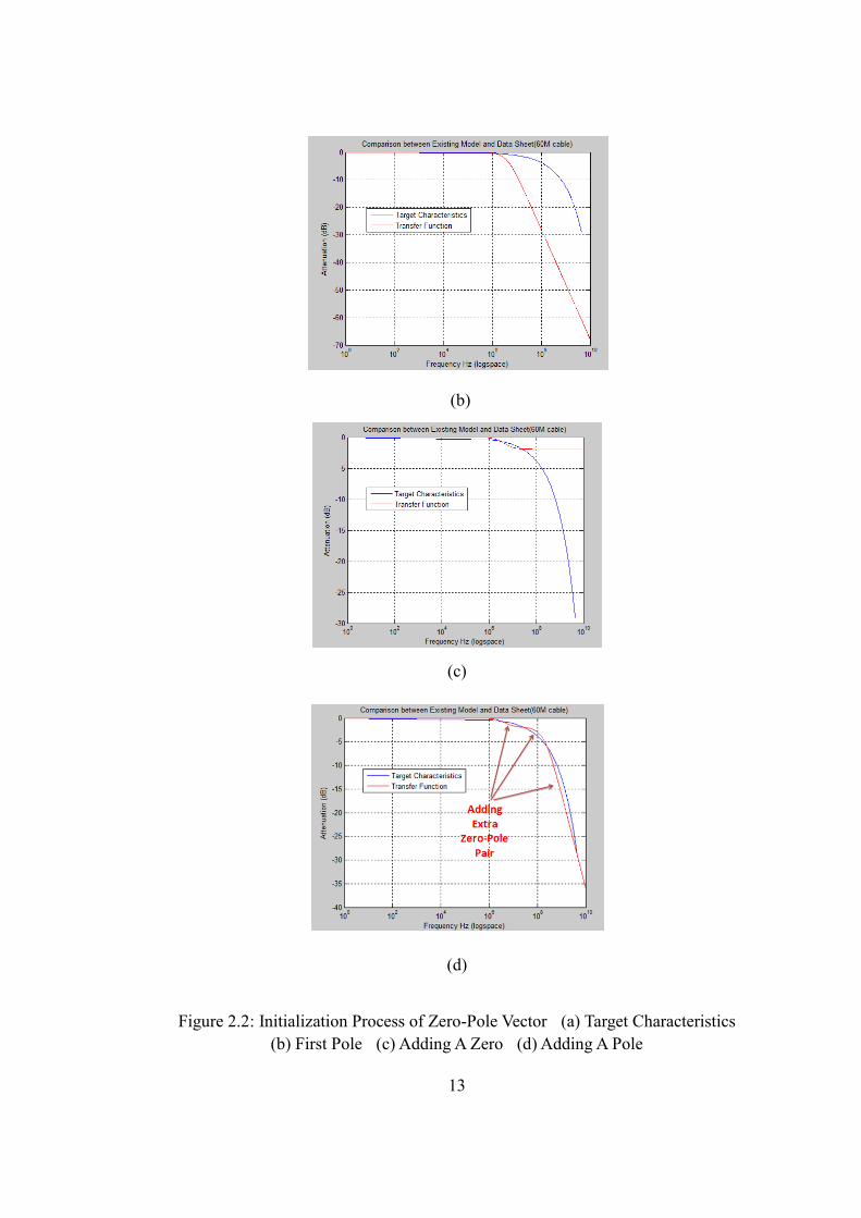
the steps illustrated in Figure 2.2. In Figure 2.2(a), sweeping the attenuation along the
characteristic curve, the first pole was added to the vector when the attenuation reached
a certain value. The transfer function with only one pole was plotted as shown in
Figure 2.2(b). Sweeping the error between the target characteristics and the transfer
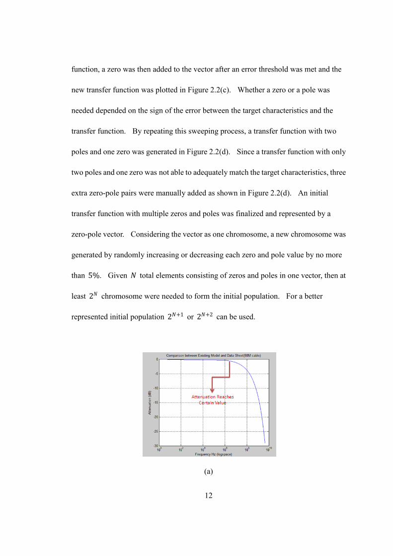
12
function, a zero was then added to the vector after an error threshold was met and the
new transfer function was plotted in Figure 2.2(c). Whether a zero or a pole was
needed depended on the sign of the error between the target characteristics and the
transfer function. By repeating this sweeping process, a transfer function with two
poles and one zero was generated in Figure 2.2(d). Since a transfer function with only
two poles and one zero was not able to adequately match the target characteristics, three
extra zero-pole pairs were manually added as shown in Figure 2.2(d). An initial
transfer function with multiple zeros and poles was finalized and represented by a
zero-pole vector. Considering the vector as one chromosome, a new chromosome was
generated by randomly increasing or decreasing each zero and pole value by no more
than 5%. Given 𝑁 total elements consisting of zeros and poles in one vector, then at
least 2𝑁 chromosome were needed to form the initial population. For a better
represented initial population 2𝑁+1 or 2𝑁+2 can be used.
(a)
13
(b)
(c)
(d)
Figure 2.2: Initialization Process of Zero-Pole Vector (a) Target Characteristics
(b) First Pole (c) Adding A Zero (d) Adding A Pole
14
After initializing the original population with the initial vector, the fitness function
was defined as the maximum absolute value of error between the target characteristic
and the transfer function response in the range from 0 Hz to roughly 4.5 GHz. The
lowest the fitness function value represented the most fit the transfer function. The
termination condition was set to 0.25 dB, implying that when the fitness function value
of a vector among the population was smaller than 0.25 dB, the evolution would be
terminated and the transfer function represented by this vector was selected as the
optimal solution.
According to the fitness function value, the population was divided into three
groups: the top 15% vectors belong to the fittest group, the bottom 15% are the least fit
and will be removed, and the remainder was the normal group.
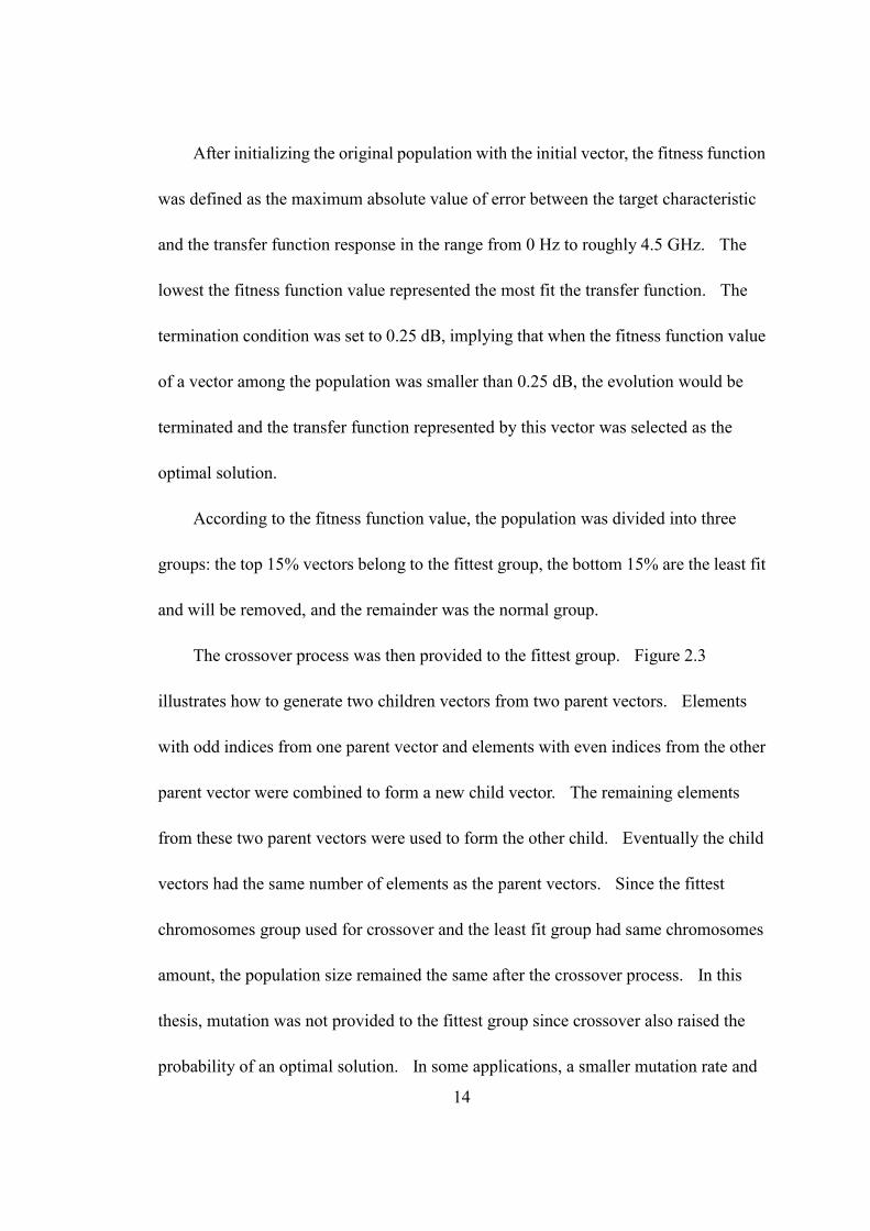
The crossover process was then provided to the fittest group. Figure 2.3
illustrates how to generate two children vectors from two parent vectors. Elements
with odd indices from one parent vector and elements with even indices from the other
parent vector were combined to form a new child vector. The remaining elements
from these two parent vectors were used to form the other child. Eventually the child
vectors had the same number of elements as the parent vectors. Since the fittest
chromosomes group used for crossover and the least fit group had same chromosomes
amount, the population size remained the same after the crossover process. In this
thesis, mutation was not provided to the fittest group since crossover also raised the
probability of an optimal solution. In some applications, a smaller mutation rate and
15
smaller mutation probability are used for the fittest group in order to increase the
evolution speed.
Figure 2.3: Crossover Process
Mutation was only provided to normal chromosomes in this thesis. The mutation
probability was set to 1, which means every element in each chromosome needs to
mutate. Mutation rate was ±5%, which means all zeros and poles values in every
chromosomes were randomly increased or decreased by no more than 5% of their
original values.
With all these genetic algorithm operators defined above, the entire genetic
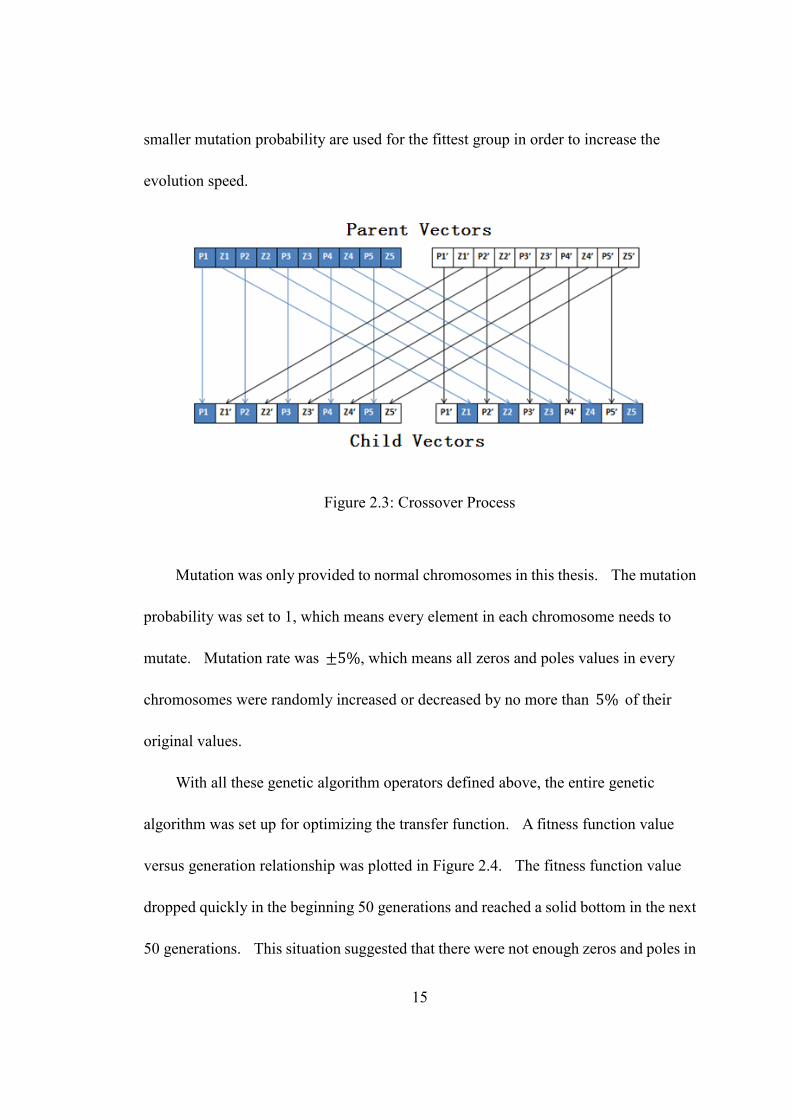
algorithm was set up for optimizing the transfer function. A fitness function value
versus generation relationship was plotted in Figure 2.4. The fitness function value
dropped quickly in the beginning 50 generations and reached a solid bottom in the next
50 generations. This situation suggested that there were not enough zeros and poles in
16
a single chromosome.
Figure 2.4: Fitness Function Value over Generations
A solution was implemented by checking if the fitness function value had not
changed in a certain number of generations. An extra zero-pole pair then need to be
added to every chromosome located around where the maximum error between the
target process and the transfer function frequency response appears. After adding this
pair, the new population was set as the initial population and the genetic algorithm
restarted. This process was finished automatically by the program itself and it should
be repeated when the fitness function value hit another bottom again.
Using the methods above, a 60 m Belden 1694A coaxial cable model transfer
function was optimized to:
5 4 3 2
7 6 5 4 3 2
3.03 44 1.92 34 3.618 25 2.368 16 5.207 08 1
9.032 64 2.41 53 1.926 43 5.705 34 7.142 25 3.588 16 6.167 08 1
e s e s e s e s e s
e s e s e s e s e s e s e s
(2.1)

17
The frequency response of this transfer function was shown in Figure 2.5. The
blue curve was the target characteristics to be modeled, the red curve was the transfer
function frequency response generated by genetic algorithm, and the green curve was
the error between the target characteristics and the transfer function frequency response.
As shown in the Figure, the absolute value of the error was always smaller than 0.25 dB
from 0 Hz to roughly 4.5 GHz.
Figure 2.5: 60 m Belden 1694A Coaxial Cable Model Results
The optimal transfer function model for different cable lengths was obtained with
same algorithm.
2.1.3 Equalizer Model
An equalizer is used to compensate cable loss. Since the cable model had already

18
been optimized, the equalizer model was obtained simply by reversing the numerator
and denominator in the cable model transfer function. In this case, the error between
the cable-equalizer combined system and the all-pass system was also within ±0.25
dB. Results similar to the cable model were shown in Figure 2.6.
Figure 2.6: 60 m Belden 1694A Coaxial Cable Equalizer Model
Extra poles were needed for the equalizer transfer function at higher frequency in
order to attenuate high frequency components after combining with cable system.
This was achieved by adding extra poles at higher frequencies in the equalizer transfer
function.

19
2.2 Adaptive Equalization
Since the cable model transfer function generated above only fits an 80 m Belden
1694A coaxial cable, it is necessary to find an adaptive method for compensating the
cable loss for lower cable lengths.
A curve-fitting method was used for adaptive equalization in this thesis. The
general transfer function was written as:
( ) 1 ( )qE s H s
(2.2)
and ( )H s was defined as:
max
1( ) 1
( )H s
C s
(2.3)
where max ( )C s was the optimal cable model transfer function for an 80 m Belden
1694A coaxial cable [7]. When =0 , the cable length is 0, then ( ) 1qE s . This
passes the original signal through since there is no cable loss. When =1 , the cable
length reaches maximum, resulting in max
1( )
( )qE s
C s . For any cable length between
0 and 80 m, there is an unique between 0 and 1 corresponding to it. By properly
tuning the value of , ( )qE s is now adaptive for any cable length smaller than the
maximum. The equalizer model frequency response with different values were
illustrated in Figure 2.7. There is a nonlinearity in the versus cable length
characteristic. This is usually not an issue since the adaptive loop eventually settles at
the optimal point [7].
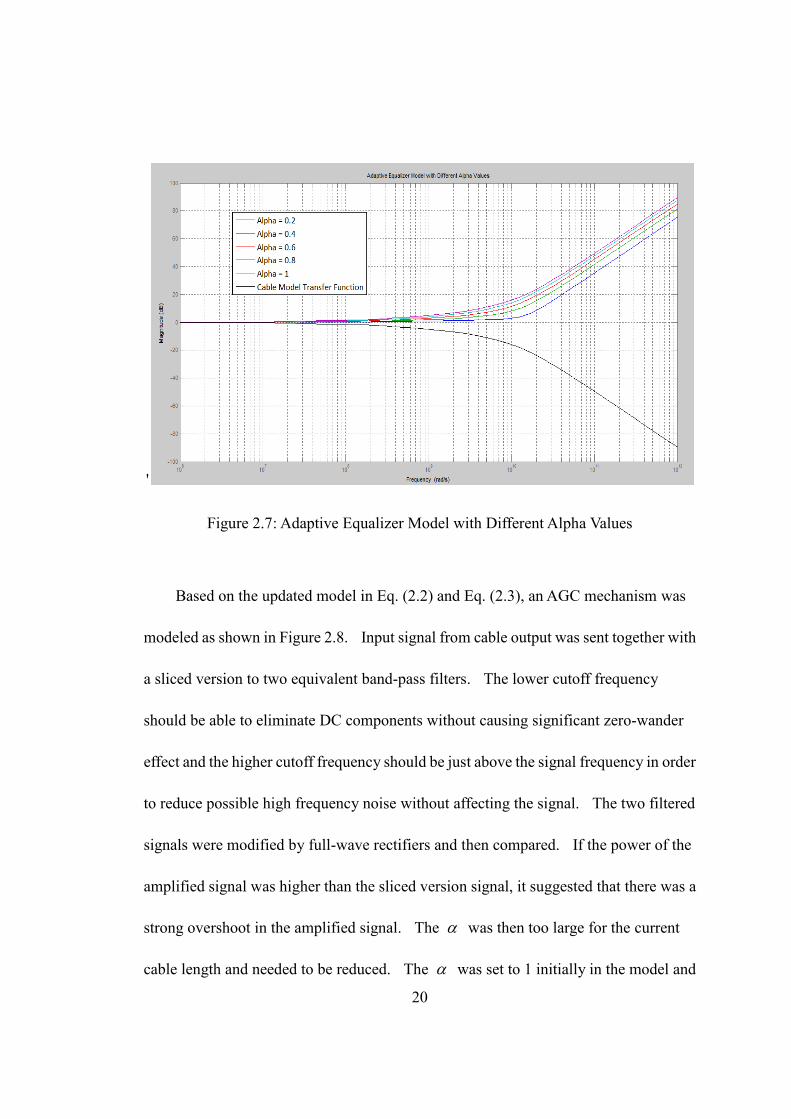
20
'
Figure 2.7: Adaptive Equalizer Model with Different Alpha Values
Based on the updated model in Eq. (2.2) and Eq. (2.3), an AGC mechanism was
modeled as shown in Figure 2.8. Input signal from cable output was sent together with
a sliced version to two equivalent band-pass filters. The lower cutoff frequency
should be able to eliminate DC components without causing significant zero-wander
effect and the higher cutoff frequency should be just above the signal frequency in order
to reduce possible high frequency noise without affecting the signal. The two filtered
signals were modified by full-wave rectifiers and then compared. If the power of the
amplified signal was higher than the sliced version signal, it suggested that there was a
strong overshoot in the amplified signal. The was then too large for the current
cable length and needed to be reduced. The was set to 1 initially in the model and
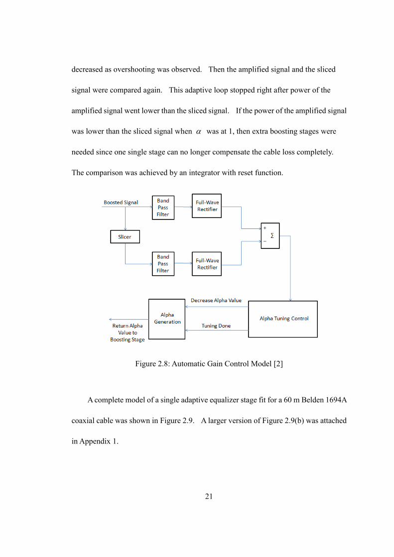
21
decreased as overshooting was observed. Then the amplified signal and the sliced
signal were compared again. This adaptive loop stopped right after power of the
amplified signal went lower than the sliced signal. If the power of the amplified signal
was lower than the sliced signal when was at 1, then extra boosting stages were
needed since one single stage can no longer compensate the cable loss completely.
The comparison was achieved by an integrator with reset function.
Figure 2.8: Automatic Gain Control Model [2]
A complete model of a single adaptive equalizer stage fit for a 60 m Belden 1694A
coaxial cable was shown in Figure 2.9. A larger version of Figure 2.9(b) was attached
in Appendix 1.

22
(a)
(b)
Figure 2.9: Model of A Single Adaptive Equalizer Stage (a) Block Diagram (b)Entire
Model
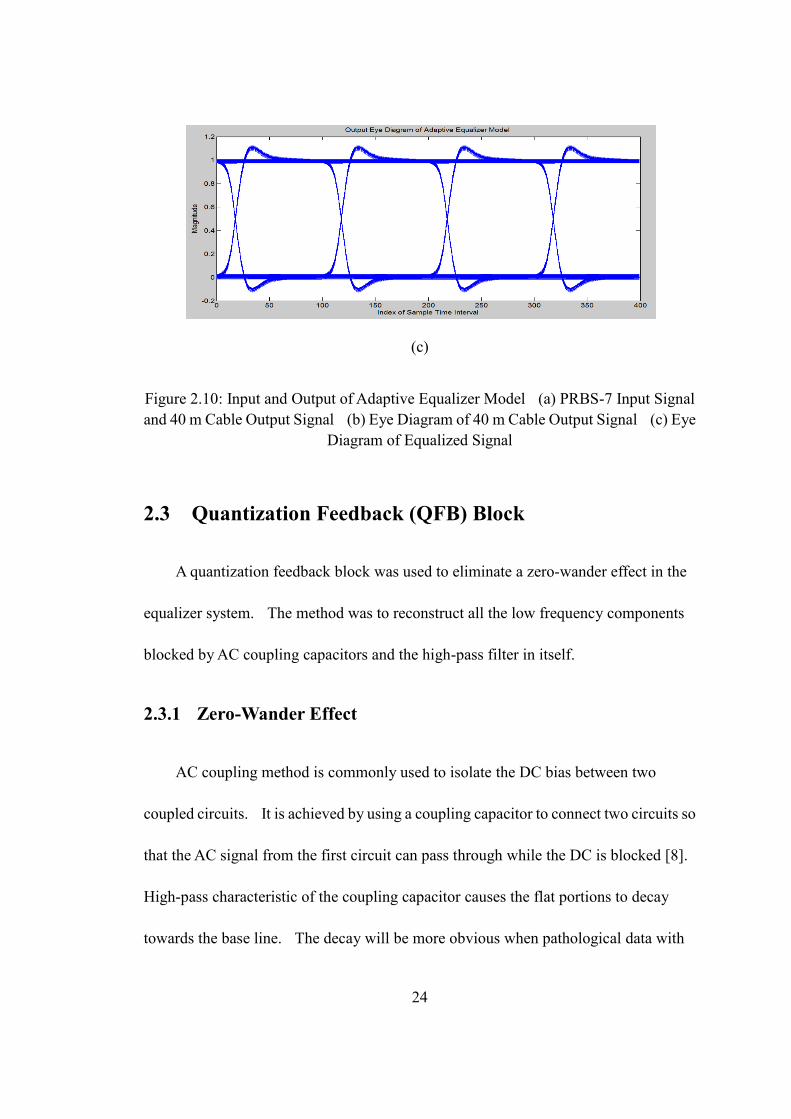
The red blocks were the PRBS-7 input and the cable model transfer function.
The PRBS-7 data were sent through a 40 m cable model transfer function. The
attenuated output, shown in Figure 2.10(a) and (b), were sent to the equalizer as the
input. Orange blocks were the boosting stages, multiplying the value of with a

23
transfer function. The values were generated by the purple blocks with initial
values of set to 1. The blue blocks compared the power of the amplified signal and
the sliced version. The result of the comparison was processed by the cyan blocks to
decide whether to decrease value or terminate the adaptive process. The eye
diagram of the output from the adaptive equalizer model was shown in Figure 2.10(c).
Although there was some overshoot, the power of the amplified signal was already
lower than the sliced signal due to the rising and falling slope. Larger threshold values
for the slicer could be used to reduce the overshoot.
(a)
(b)
24
(c)
Figure 2.10: Input and Output of Adaptive Equalizer Model (a) PRBS-7 Input Signal
and 40 m Cable Output Signal (b) Eye Diagram of 40 m Cable Output Signal (c) Eye
Diagram of Equalized Signal
2.3 Quantization Feedback (QFB) Block
A quantization feedback block was used to eliminate a zero-wander effect in the
equalizer system. The method was to reconstruct all the low frequency components
blocked by AC coupling capacitors and the high-pass filter in itself.
2.3.1 Zero-Wander Effect
AC coupling method is commonly used to isolate the DC bias between two
coupled circuits. It is achieved by using a coupling capacitor to connect two circuits so
that the AC signal from the first circuit can pass through while the DC is blocked [8].
High-pass characteristic of the coupling capacitor causes the flat portions to decay
towards the base line. The decay will be more obvious when pathological data with
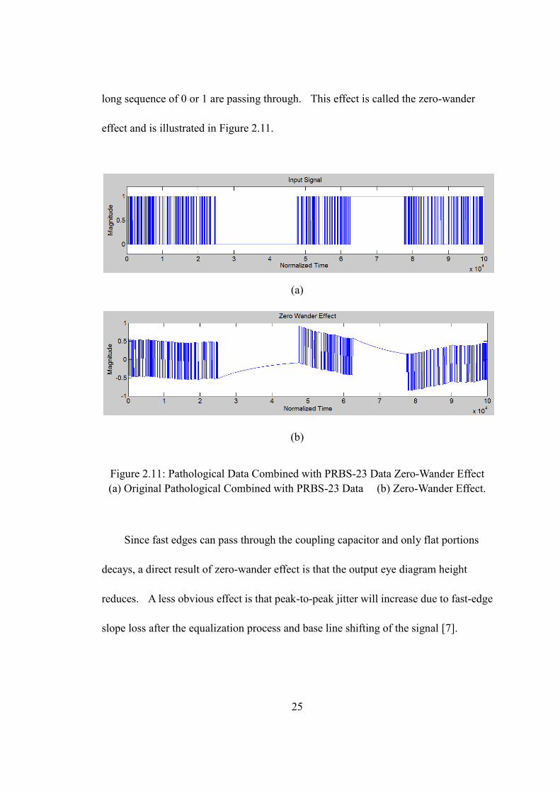
25
long sequence of 0 or 1 are passing through. This effect is called the zero-wander
effect and is illustrated in Figure 2.11.
(a)
(b)
Figure 2.11: Pathological Data Combined with PRBS-23 Data Zero-Wander Effect
(a) Original Pathological Combined with PRBS-23 Data (b) Zero-Wander Effect.
Since fast edges can pass through the coupling capacitor and only flat portions
decays, a direct result of zero-wander effect is that the output eye diagram height
reduces. A less obvious effect is that peak-to-peak jitter will increase due to fast-edge
slope loss after the equalization process and base line shifting of the signal [7].

26
2.3.2 Quantization Feedback Modeling
An effective method to eliminate the zero-wander effect is the quantization
feedback (QFB) method. A QFB block is formed by a high-pass filter, a low-pass filter,
and a slicer, as shown in Figure 2.12.
Figure 2.12: QFB Block Illustration
The high-pass filter and low-pass filter should have the same cutoff frequency.
This cutoff frequency should be higher than the cutoff frequencies of any AC coupling
filters. The threshold of the slicer should be set at the middle between 0 and 1 levels
[7].
The high-pass filter removes all the low frequency components from the input
signal. The slicer then generates a new DC level for the high-pass filter output. The
slicer output goes to the low-pass filter. Since the low-pass filter has the same cutoff
frequency as the high-pass filter, all the high frequency components left from the

27
high-pass filter are gone, and low frequency components associated with the new DC
level remain. A new signal with entire spectrums can be reconstructed by adding the
output of the high-pass filter and the output of the low-pass filter. It is important that
the cutoff frequencies of both filters are higher than the cutoff frequencies of all the AC
coupling filters, otherwise the spectrum between the cutoff frequency of the QFB block
and the AC coupling filters will not be able to be constructed by the low-pass filter. A
typical QFB block was modeled as shown in Figure 2.13.
Figure 2.13: Typical QFB Simulink Model
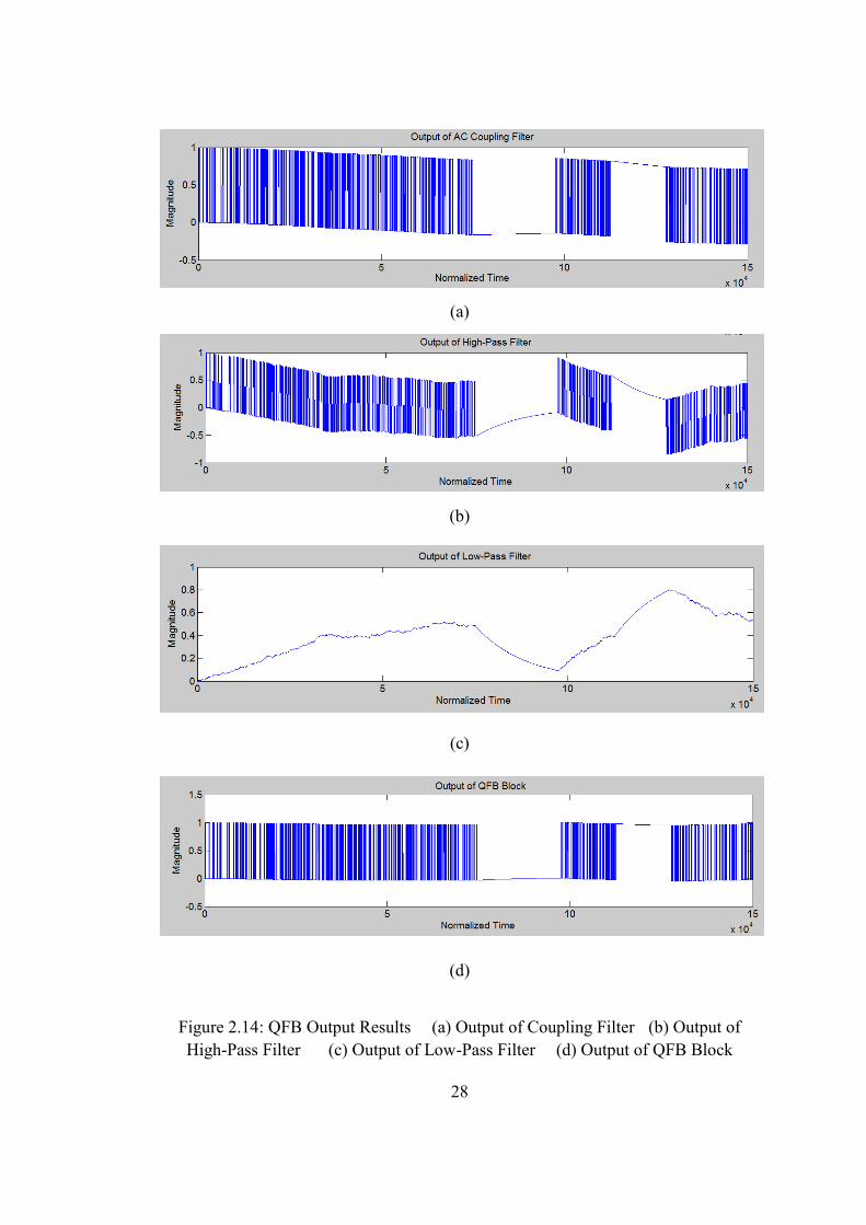
The outputs of every stage in QFB block were illustrated in Figure 2.14. The
zero-wander effect could be seen in the output of the AC coupling filter in Figure
2.14(a). Figure 2.14(b) was the output of the high-pass filter in QFB block. Since a
higher cutoff frequency was used, more zero-wander effect was observed. Figure
2.14(c) was the output of the low-pass filter in QFB block. All the sharp edges ere
removed due to the low-pass response and a new DC level was generated. Figure
2.14(d) was the output of the entire QFB block, showing that all the zero-wander effect
was eliminated.
28
(a)
(b)
(c)
(d)
Figure 2.14: QFB Output Results (a) Output of Coupling Filter (b) Output of
High-Pass Filter (c) Output of Low-Pass Filter (d) Output of QFB Block

29
2.4 Adaptive Equalizer Model with QFB Block
The complete equalizer system model consisted of two main blocks: a cascade of
three adaptive equalizer stages and the QFB. The AGC mechanism was embedded in
every adaptive equalizer stage. Boosting gain was tuned properly inside each stage
before the signal passes to next stage. An alternate way for tuning is to build an extra
AGC block controlling all three values together in all three stages [2]. These two
ways had the same time cost in simulation, so in this work the first method was used.
The entire system model was shown in Figure 2.15. Each equalizer stage was
able to compensate a maximum of an 80 m Belden 1694A coaxial cable and adaptively
tuned for any shorter cable length. The entire system was fit for 240 m maximum.
Figure 2.15: Complete Equalizer System Model
30
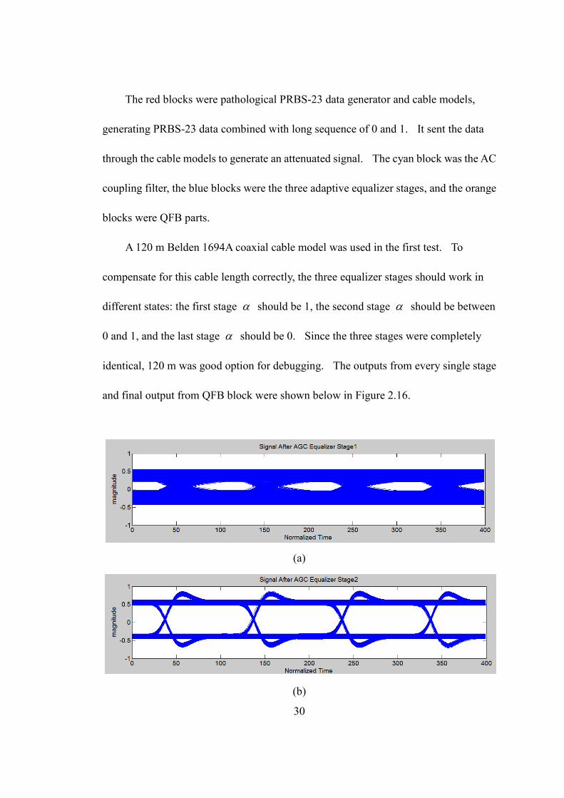
The red blocks were pathological PRBS-23 data generator and cable models,
generating PRBS-23 data combined with long sequence of 0 and 1. It sent the data
through the cable models to generate an attenuated signal. The cyan block was the AC
coupling filter, the blue blocks were the three adaptive equalizer stages, and the orange
blocks were QFB parts.
A 120 m Belden 1694A coaxial cable model was used in the first test. To
compensate for this cable length correctly, the three equalizer stages should work in
different states: the first stage should be 1, the second stage should be between
0 and 1, and the last stage should be 0. Since the three stages were completely
identical, 120 m was good option for debugging. The outputs from every single stage
and final output from QFB block were shown below in Figure 2.16.
(a)
(b)

31
(c)
(d)
Figure 2.16: 120 m Belden 1694A Coaxial Cable Equalization Results (a)Output
of Stage1 (b)Output of Stage2 (b)Output of Stage3 (d)Output of Entire System
The first stage compensated for the 80 m cable loss completely, so the eye diagram
of the output from the first stage showed the original signal with a 40 m cable loss.
The second stage compensated for this 40 m cable loss and the signal was fully
recovered. The third stage did nothing to the signal. The QFB block fixed the
zero-wander effect, so the eye height of the final output from QFB block was larger
than that in the second and third stage outputs. The 𝛼 value in the first stage was 1, in
the second stage was 0.41, in the third stage was 0, as expected. Different slicer
threshold values were used in different simulations to graphically depict the overshoot

32
differences caused by them. In this simulation, a large threshold value was used so
there was not much overshoot.
Other tests using different cable lengths were also made. 40 m cable and 200 m
cable were used to check the adaptive function of each stage while 20 m cable and 240
m cable were used to check if the equalizer is still functional when a very short or very
long cable was used.
The 40 m cable results were shown in Figure 2.17. A smaller slicer threshold
value was used in this simulation so the overshoot increased noticeably. The first stage
compensated for all the cable loss so the second and third stages did nothing. The 𝛼
value of the first stage was still 0.41, and the 𝛼 values of second stage and third stage
were both 0.
(a)
(b)
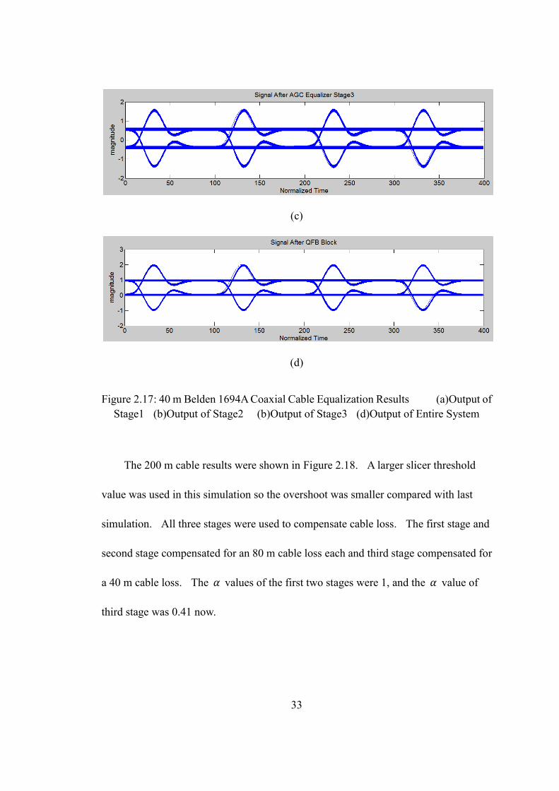
33
(c)
(d)
Figure 2.17: 40 m Belden 1694A Coaxial Cable Equalization Results (a)Output of
Stage1 (b)Output of Stage2 (b)Output of Stage3 (d)Output of Entire System
The 200 m cable results were shown in Figure 2.18. A larger slicer threshold
value was used in this simulation so the overshoot was smaller compared with last
simulation. All three stages were used to compensate cable loss. The first stage and
second stage compensated for an 80 m cable loss each and third stage compensated for
a 40 m cable loss. The 𝛼 values of the first two stages were 1, and the 𝛼 value of
third stage was 0.41 now.

34
(a)
(b)
(c)
(d)
Figure 2.18: 200 m Belden 1694A Coaxial Cable Equalization Results (a)Output
of Stage1 (b)Output of Stage2 (b)Output of Stage3 (d)Output of Entire System

35
The 240 m cable results were shown in Figure 2.19. There was almost no
overshoot since this was the maximum cable length could be handled by this system.
All three stages were used to compensate for cable loss with each stage compensating
for an 80 m cable loss. The 𝛼 values of all three stages were 1 now.
(a)
(b)
(c)
36
(d)
Figure 2.19: 240 m Belden 1694A Coaxial Cable Equalization Results (a)Output
of Stage1 (b)Output of Stage2 (b)Output of Stage3 (d)Output of Entire System
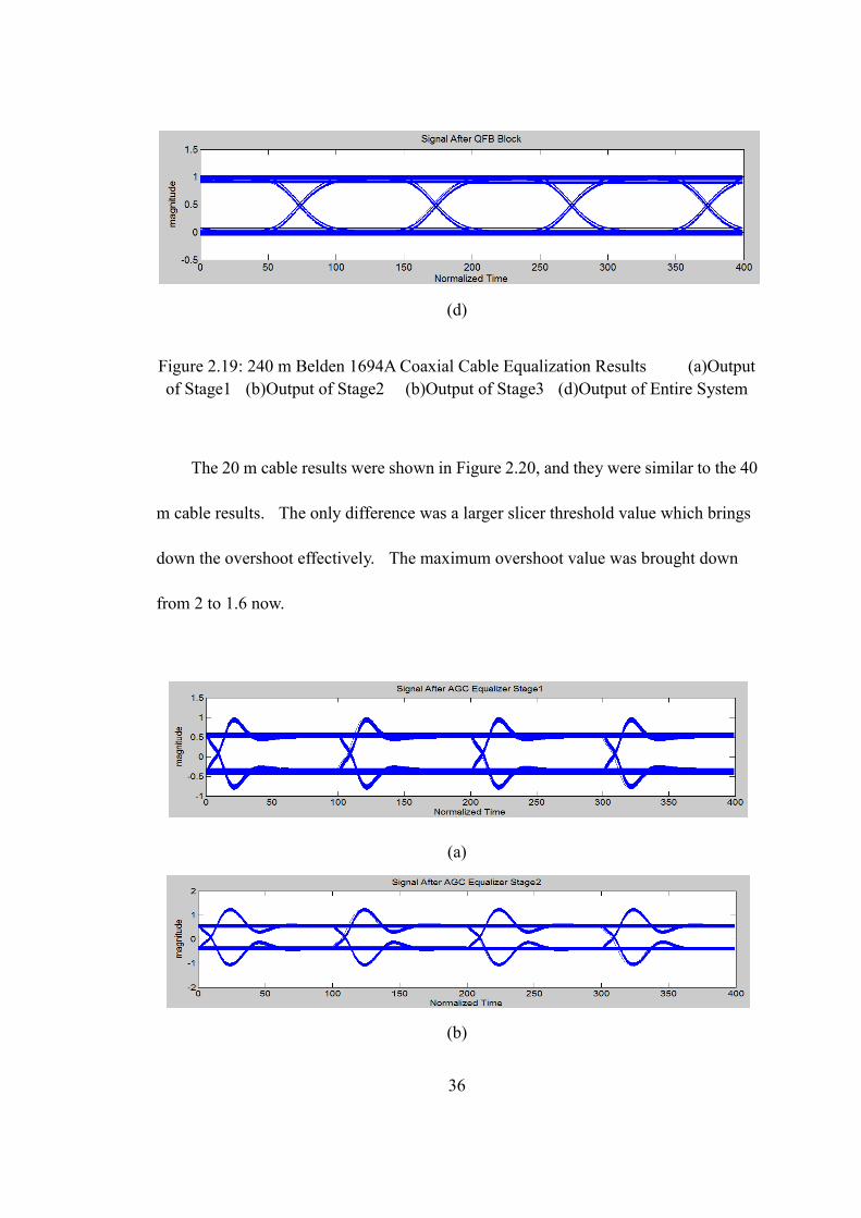
The 20 m cable results were shown in Figure 2.20, and they were similar to the 40
m cable results. The only difference was a larger slicer threshold value which brings
down the overshoot effectively. The maximum overshoot value was brought down
from 2 to 1.6 now.
(a)
(b)

37
(c)
(d)
Figure 2.20: 20 m Belden 1694A Coaxial Cable Equalization Results (a)Output of
Stage1 (b)Output of Stage2 (b)Output of Stage3 (d)Output of Entire System
From the results presented above, a conclusion can be made that the three stages
adaptive equalizer model with QFB block was adaptively working for maximum 240 m
Belden 1694A coaxial cable. For all the final outputs of the QFB block, the eye
heights were around 1 and the peak-to-peak jitters were less than 0.1 UI.
Chapter 3. Circuit Implementation
3.1 Methodology
The key part to transferring the existing design into CMOS circuit is the adaptive
filter stage. Following the adaptive equalizer model in the last chapter, a CMOS

38
adaptive equalizer stage was designed to adaptively compensate for a maximum 80 m
Belden 1694A coaxial cable.
A typical design flow was illustrated in Figure 3.1. The first step is to build an
amplifier with a flat low-pass frequency response. The cutoff frequency of this
low-pass response should be slightly larger than the signal frequency, so that the entire
spectrum will pass and only noise with higher frequency will be attenuated. The next
step is to tune the frequency response to match the reverse cable characteristic. An RC
degeneration method is used to reduce the DC gain and extra RC pairs are used to
generate additional zero-pole pairs in frequency to make it closer to the target
characteristic. The final step is to build a Variable Gain Amplifier(VGA) for gain
tuning, which makes the equalizer adaptive for different cable length.
(a)

39
(b)
(c)
Figure 3.1: Design Flow of Equalizer (a) Flat Response (b) RC Degeneration and
Tuning (c) Variable Gain Control
The circuit was implemented in GPDK 45 nm CMOS technology and simulated in
Cadence environment. For an 80 m Belden 1694A coaxial cable, the cable loss at 1.5
GHz was 21 dB. Two methods were used to realize the steps in Figure 3.1. The first
one was to design a pre-amplifier stage offering enough gain and bandwidth with a
VGA stage used as an attenuator for adaptive consideration. RC degeneration was
40
added to both stages for tuning the frequency response close to the reverse cable
characteristic. A folded cascode amplifier and a folded Gilbert cell were used in this
method as the pre-amplifier and the VGA, respectively. The second method used an
RC degenerated pre-amplifier and VGA together to generate the required gain. In the
second method, a single differential amplifier was used as the pre-amplifier stage since
the gain requirement was not as strict as in the first method. A folded Gilbert cell was
still used as the VGA stage.
3.2 Differential Amplifier
A CMOS differential amplifier implemented with GPDK 45 nm technology was
shown in Figure 3.2. Since this amplifier was used to drive another CMOS circuit in
45 nm technology and currently ggC of NM0 and NM1 were 47 fF, the load capacitor
value was set to 60 fF to match the future design. The DC gain of the amplifier was
[9]:
( 0) ( 0) ( 0)( || )v m NM DS PM DS NMA g R R
(3.1)
and we also knew:
( 0) ( 2)
( 0)
( 0)
n ox NM DS NM
m NM
NM
C W Ig
L
(3.2)
and the bandwidth of the amplifier was [9]:
( 0) ( 0)
1
( || )DS PM DS NM loadR R C
(3.3)

41
I_bias
NM3 NM4
PM3
V_bias_P
V_bias_N
V_bias_P V_bias_PPM0 PM2
NM0 NM1
NM2
Input+ Input-
V_bias_N
Output
Figure 3.2: CMOS Differential Amplifier in GPDK 45 nm Technology
According to Eq. (3.1), Eq. (3.2), and Eq. (3.3), there was a tradeoff between the
DC gain and the bandwidth. Without changing load capacitance, the only way to
improve the bandwidth was to decrease ( 0) ( 0)||DS PM DS NMR R , which caused a reduction
in vA according to Eq. (3.1). Increasing
( 0)m NMg was achieved by increasing
( 0)NMW or ( 2)DS NMI . If
( 0)NMW was increased, ( 0) ( 0)||DS PM DS NMR R was decreased and
bandwidth went down; if ( 2)DS NMI was increased, to maintain all the transistors
working in saturation mode, ( 0)NMW and ( 0)PMW should be increased,
( 0) ( 0)||DS PM DS NMR R was then decreased and bandwidth was also decreased. The bias
current I_bias was selected based on the output slew rate. The data rate of the signal

42
was 1.5 Gbps. One bit period was 666.7 ps, assuming the rising and falling edges take
no more than 60 ps each and the output signal swing was 400 mV based on current data
transmission standard. For each differential output branch, the swing should be 200
mV and the slew rate as 3.33 mV/ps, since the slew rate was defined as:
DS
load
ISR
C
(3.4)
and minimum DSI was calculated by:
315 4
12
200 1060 10 2 10
60 10DS loadI SR C
A (3.5)
The tail current of the differential amplifier should be at least 0.4 mA. Giving
design margins for the corner conditions, I_bias was set to 4 mA in this thesis.
All the transistor sizes and devices parameters were listed in table 2.
Table 2. Transistor Sizes and Devices Parameters of 45 nm Differential Amplifier
Element W/L Element W/L Element Value
PM0 45nm/48um NM0 45nm/68um I_bias 4 mA
PM2 45nm/48um NM1 45nm/68um Vgs 0.8 V
PM3 45nm/48um NM2 45nm/120um C_load 60 fF
NM3 45nm/82um NM4 45nm/48um VDD 1 V
The frequency response of the differential amplifier was shown in Figure 3.3.

43
Figure 3.3: Frequency Response of the Differential Amplifier
The DC gain of the differential amplifier was 15.8 dB and gain at 1.5 GHz was
15.05 dB. It suggested that if a single stage differential amplifier was used as a
pre-amplifier, the VGA stage should also be able to offer around 10 dB gain to fully
compensate for the 80 m Belden 1694A coaxial cable at 1.5 GHz.
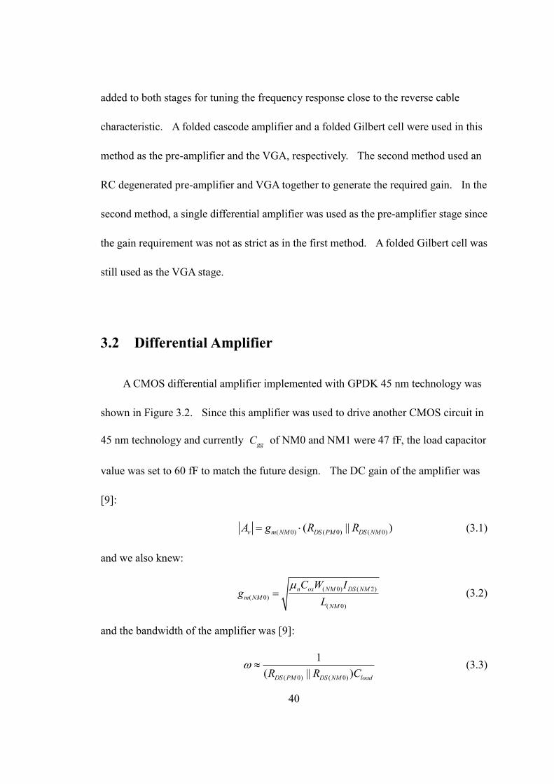
3.3 Wide Swing Current Mirror and Folded Cascode
The wide swing current mirror [10], also known as the low-voltage cascode mirror
[9], is used to increase signal swing in cascode mirror.
A typical wide swing current mirror was shown in Figure 3.4. The transistors
sizes were set as 1 1 4 43 3 2 22 2
/ // /
W L W LW L W L
n n
and 3 3
5 52
//
W LW L
n .
44
I_bias
N5
N3
I_in
N4
N2
I_out
N1
Figure 3.4: Wide Swing Current Mirror
According to the transistors sizes, assume I_bias = I_in = I_out, then it is known
that 2 3
2 2
2 _
( / )eff eff eff
n ox
I biasV V V
C W L
since N5 has the same DSI but is 2( 1)n times smaller,
then 5 ( 1)e f f e f fV n V
and 1 4eff eff effV V nV
thus it is known that
5 4 1 ( 1)G G G eff thV V V n V V
furthermore, since 1 4GS GSV V ,
so 2 3 5 1 5 ( )DS DS G GS G eff th effV V V V V nV V V
This DSV puts N2 and N3 at the edge of linear region. Thus the minimum
allowable output voltage is
45
1 2 ( 1)out eff eff effV V V n V
if 1n ,
then 2out effV V
also it is required that
4 4DS eff effV V nV
since
4 3 3 ( )DS G DS eff th eff thV V V V V V V
it is not hard to achieve.
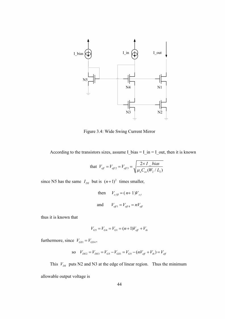
A typical folded cascode amplifier was shown in Figure 3.5.
M3
M5
M7
M9
M1 M2
M11
M10
M8
M6
M4
Input+ Input-
Output- Output+
Figure 3.5: Folded Cascode Amplifier
The advantage of folded cascode amplifier is higher DC gain compared with a
46
single stage differential amplifier, but output swing is limited due to the four stacks of
transistors between VDD and GND. The wide swing current mirror is introduced for
properly biasing the folded cascode amplifier at a lower voltage.
DC gain of the folded cascode is:
1 5 5 5 3 1 7 7 7 9( ) ( || ) || ( )v m m mb DS DS DS m mb DS DSA g g g R R R g g R R
(3.6)
and the bandwidth is:
5 5 5 3 1 7 7 7 9 7 5
1
( ) ( || ) || ( ) ( )m mb DS DS DS m mb DS DS GD GD loadg g R R R g g R R C C C
(3.7)
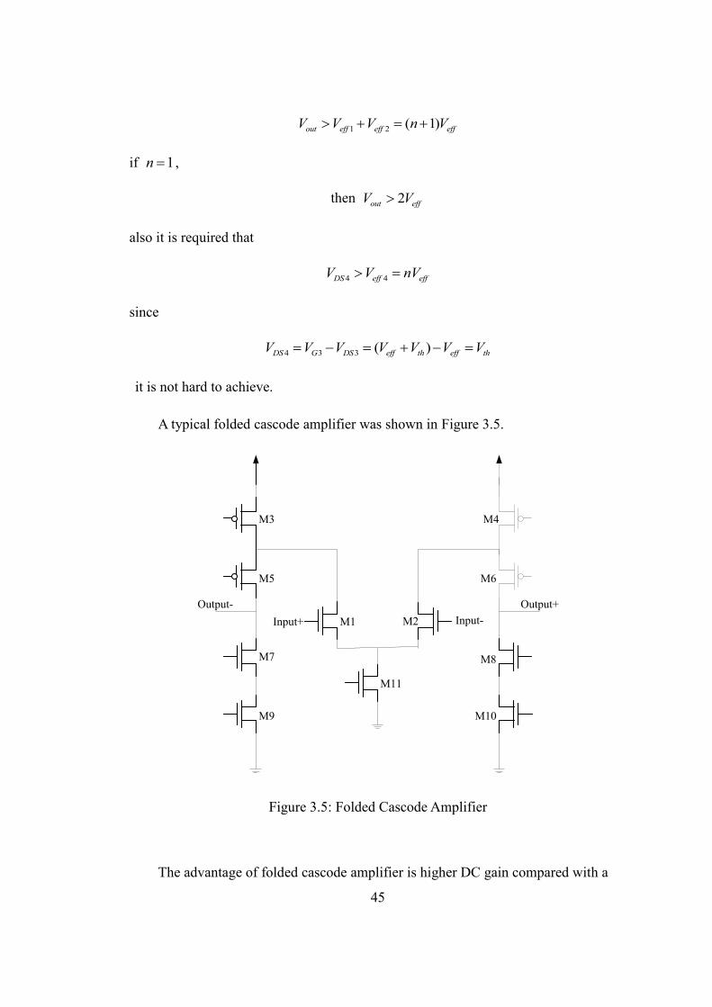
A folded cascode biased with wide swing current mirror was shown in Figure 3.6.
A larger version of Figure 3.6(a) was in Appendix 2.
I_bias
NM0 NM5
PM7
V_bias_tailNM1
PM8
PM9
V_bias_tail
V_bias_pm
V_bias_ptPM10
PM12
NM7
V_bias_pt
V_bias_pm
NM8
NM9
PM11
PM13
V_bias_nm
V_bias_nb
PM15
PM14
NM10
NM11
NM16 NM17
NM34
NM15
NM14
PM20
PM19
Input+ Input-
Output- Output+
V_bias_pt
V_bias_pm
V_bias_nm
V_bias_nb
V_bias_tail
(a)
I_bias
NM0 NM5
PM7
V_bias_tailNM1
PM8
PM9
V_bias_tail
V_bias_pm
V_bias_ptPM10
PM12
NM7
V_bias_pt
V_bias_pm
NM8
NM9
PM11
PM13
V_bias_nm
V_bias_nb
(b)
47
PM15
PM14
NM10
NM11
NM16 NM17
NM34
NM15
NM14
PM20
PM19
Input+ Input-
Output- Output+
V_bias_pt
V_bias_pm
V_bias_nm
V_bias_nb
V_bias_tail
(c)
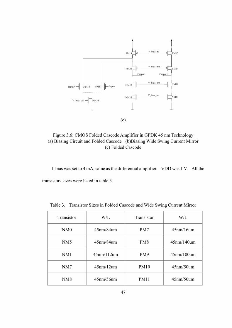
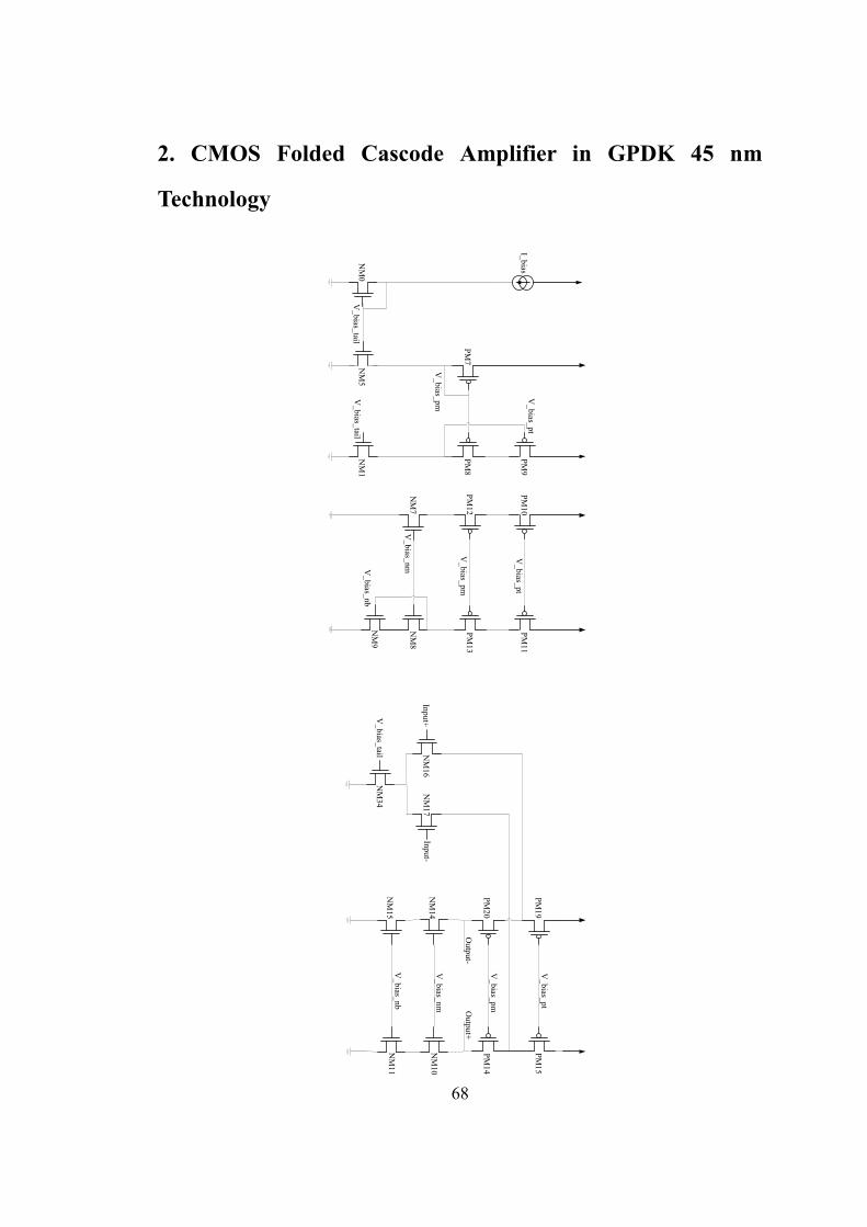
Figure 3.6: CMOS Folded Cascode Amplifier in GPDK 45 nm Technology
(a) Biasing Circuit and Folded Cascode (b)Biasing Wide Swing Current Mirror
(c) Folded Cascode
I_bias was set to 4 mA, same as the differential amplifier. VDD was 1 V. All the
transistors sizes were listed in table 3.
Table 3. Transistor Sizes in Folded Cascode and Wide Swing Current Mirror
Transistor W/L Transistor W/L
NM0 45nm/84um PM7 45nm/16um
NM5 45nm/84um PM8 45nm/140um
NM1 45nm/112um PM9 45nm/100um
NM7 45nm/12um PM10 45nm/50um
NM8 45nm/56um PM11 45nm/50um

48
NM9 45nm/64um PM12 45nm/70um
NM16 45nm/88um PM13 45nm/72um
NM17 45nm/88um PM14 45nm/72um
NM34 45nm/144um PM15 45nm/96um
NM10 45nm/56um PM19 45nm/96um
NM11 45nm/64um PM20 45nm/72um
NM14 45nm/56um NM15 45nm/64um
The frequency response of this folded cascode amplifier was shown in Figure 3.7.
The DC gain was 26.16 dB, although the bandwidth was smaller than 1.5 GHz, the gain
at 1.5 GHz was 20.8 dB, which was enough to compensate for 80 m Belden 1694A
coaxial cable.
Figure 3.7: Frequency Response of the Folded Cascode Amplifier

49
Since this amplifier was already able to offer enough gain, I used this folded
cascode amplifier as pre-amplifier stage and used a VGA as attenuator only.
3.4 Gilbert Cell and Folded Gilbert Cell
A Gilbert cell consists of two differential amplifiers, as shown in Figure 3.8.
Vin+ Vin+
Vout- Vout+
Vc+ Vc-
Vin-
M1
M2 M3
M4 M5 M6 M7
Figure 3.8: Gilbert Cell
Tail current from M1 splits into M2 and M3 and controlled by voltage pair Vc+
and Vc-. When Vc+ equals Vc- with same tail current, the two differential amplifiers
will have equivalent performance, thus both of the outputs are 0 since M5-M6 and
M4-M7 pairs will have fully differential outputs and cancel each other when coupled as
shown. When Vc+ and Vc- are not equal, 2DSI is not equal to 3DSI , and

50
2 3 1DS DS DSI I I . The current at Vout- is 2 3
2
DS DSI I and current at Vout+ is
3 2
2
DS DSI I, a fully differential output is generated, and the gain is tuned by 2DSI
and
3DSI . These currents are controlled by Vc- and Vc+.
The maximum gain of the Gilbert cell appears when M2 or M3 is turned off and all
tail current flows through the other transistor. The maximum gain of the Gilbert cell is
roughly equal to sum of the two differential amplifier gains.
Considering the active load, there are four total stacked transistors in the Gilbert
cell from VDD to GND. A folded version of Gilbert cell is presented in [11], [12], and
[13], with three stacks only allowing for more headroom.
A folded Gilbert cell implemented in GPDK 45 nm technology was depicted in
Figure 3.9. Transistors sizes were decided in the same way as the differential amplifier.
An important fact was for best linearity performance, 3/4 1/2
1( ) ( )
7
W W
L L should be
used [14].
Vin+ Vin+Vin-
Vout- Vout+
VGA_CMVGA_CM
M3
M4
M1 M2Vc+ Vc-
Figure 3.9: CMOS Folded Gilbert Cell in GPDK 45 nm Technology
51
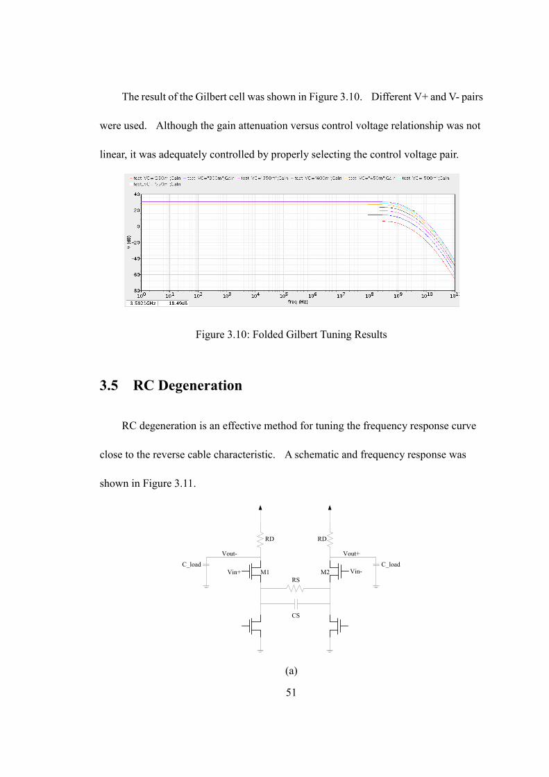
The result of the Gilbert cell was shown in Figure 3.10. Different V+ and V- pairs
were used. Although the gain attenuation versus control voltage relationship was not
linear, it was adequately controlled by properly selecting the control voltage pair.
Figure 3.10: Folded Gilbert Tuning Results
3.5 RC Degeneration
RC degeneration is an effective method for tuning the frequency response curve
close to the reverse cable characteristic. A schematic and frequency response was
shown in Figure 3.11.
RD RD
Vin+ Vin-
Vout+Vout-
C_loadC_load
M1 M2
RS
CS
(a)
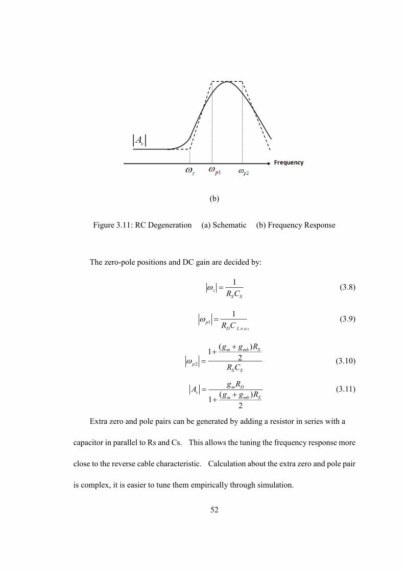
52
(b)
Figure 3.11: RC Degeneration (a) Schematic (b) Frequency Response
The zero-pole positions and DC gain are decided by:
1z
S SR C
(3.8)
1
1p
D L o a dR C
(3.9)
2
( )1
2m mb S
p
S S
g g R
R C
(3.10)
( )1
2
m Dv
m mb S
g RA
g g R
(3.11)
Extra zero and pole pairs can be generated by adding a resistor in series with a
capacitor in parallel to Rs and Cs. This allows the tuning the frequency response more
close to the reverse cable characteristic. Calculation about the extra zero and pole pair
is complex, it is easier to tune them empirically through simulation.

53
A target frequency response values at specific frequency points for 80 m Belden
1694A coaxial cable were listed in table 4.
Table 4. Target Frequency Response for 80 m Belden 1694A Coaxial Cable
3.6 Folded Cascode Amplifier Type Equalizer Stage
Combining the folded cascode amplifier implemented before with the folded
Gilbert cell, an equalizer stage was generated, then the frequency response was tuned
following the values from table 4.
The schematic and the simulation results were shown in Figure 3.12. A larger
version of Figure 3.12(a) was in Appendix 3.
I_bias
V_bias_tail V_bias_tail
V_bias_pm
V_bias_pt
V_bias_pt
V_bias_pm
V_bias_nm
V_bias_nb
Input+ Input-
V_bias_pt
V_bias_pm
V_bias_nm
V_bias_nb
V_bias_tail
Vout- Vout+
VGA_CMVGA_CM
Vc+ Vc-
V_bias_tail
(a)
Frequency 1 MHz 10 MHz 100 MHz 1 GHz 1.5 GHz
Boosting
Value
Almost
0 dB
1.7 dB 4.9 dB 17.1 dB 21dB
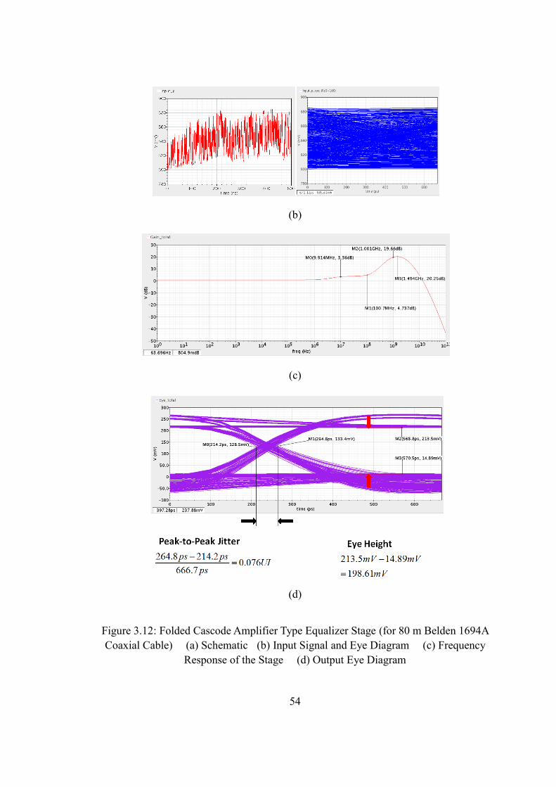
54
(b)
(c)
(d)
Figure 3.12: Folded Cascode Amplifier Type Equalizer Stage (for 80 m Belden 1694A
Coaxial Cable) (a) Schematic (b) Input Signal and Eye Diagram (c) Frequency
Response of the Stage (d) Output Eye Diagram
55
A 200 mV PRBS-23 input signal was processed by a 80 m cable model in Matlab
environment, output signal of the cable model was imported to Cadence as simulation
input as shown in Figure 3.12(b). The equalizer stage frequency response was shown
in Figure 3.12(c). Mismatch was not able to be eliminated completely, which caused
the unstable DC level and overshoot shown in Figure 3.12(d). However, the eye
height was almost 200 mV and the peak-to-peak jitter was only 0.077 UI.
3.7 Differential Amplifier Type Equalizer Stage
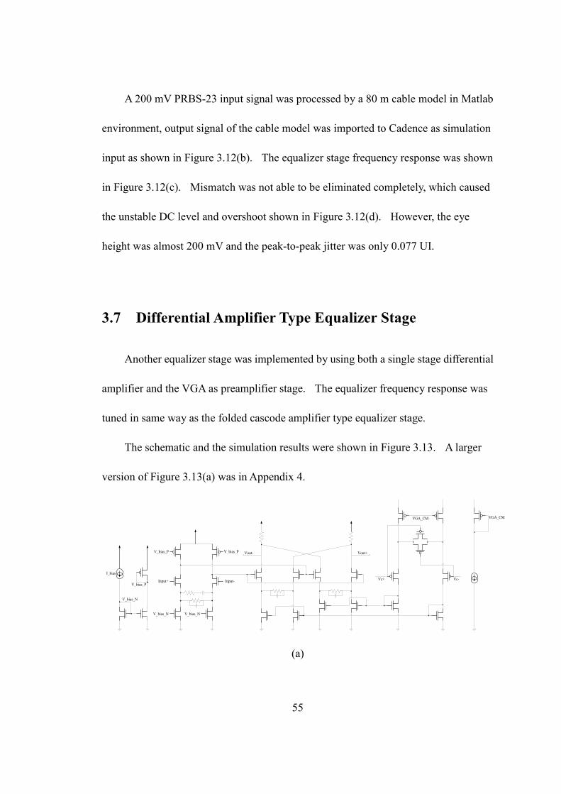
Another equalizer stage was implemented by using both a single stage differential
amplifier and the VGA as preamplifier stage. The equalizer frequency response was
tuned in same way as the folded cascode amplifier type equalizer stage.
The schematic and the simulation results were shown in Figure 3.13. A larger
version of Figure 3.13(a) was in Appendix 4.
Vout- Vout+
VGA_CMVGA_CM
Vc+ Vc-
I_bias
V_bias_P
V_bias_N
V_bias_P V_bias_P
Input+ Input-
V_bias_N V_bias_N
(a)

56
(b)
(c)
(d)
Figure 3.13: Differential Amplifier Type Equalizer Stage (for 80 m Belden 1694A
Coaxial Cable) (a) Schematic (b) Input Signal and Eye Diagram (c) Frequency
Response of the Stage (d) Output Eye Diagram

57
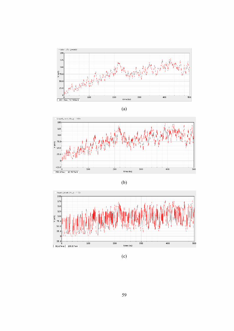
The equalizer frequency response was tuned differently in this stage so the
peak-to-peak jitter reduced by half whereas the eye height dropped slightly.
Peak-to-peak jitter and eye height in this case cannot be optimized together, since
in order to fully compensate for an 80 m Belden 1694A coaxial cable attenuation, the
equalizer frequency response should boost up 17 dB at 1 GHz and 21 dB at 1.5 GHz, a
first order zero in frequency response cannot afford such a high slope. If 21 dB at 1.5
GHz is matched, there will be a mismatch at 1 GHz, causing a peak-to-peak jitter
increment, otherwise if 17 dB at 1 GHz is matched, the equalizer can offer only 18.86
dB gain at 1.5 GHz, which causes an eye height decrease.
3.8 Adaptive Simulation Results and Cascade Simulation
Results
The adaptive ability was also tested in chapter 2.4 of this thesis. The value
should be 0.41 when the cable length was 40 m. Following same way, a PRBS-23 data
was processed in Matlab environment with 40 m cable model, the output was imported
to Cadence as input of the simulation. Since 1020 log (0.41) 7.7dB , and also:
max max
1 1( ) 1 ( ) 1 ( 1) (1 )
( ) ( )qE s H s
C s C s
(3.12)
By properly tuning the control voltage of the VGA, the frequency response
dropped by 7.7 dB, then add 0.4 times of the input signal to the output signal.

58
The final output was shown in Figure 3.14. It matched the results in Figure 2.17
very well.
Figure 3.14: Differential Amplifier Type Equalizer Stage Adaptive Output
PRBS-23 data was process with 240 m cable model in Matlab environment and
imported to Cadence as the input of three cascade equalizer stages. The input and
output of every stage was illustrated in Figure 3.15. Differential amplifier equalizer
stages were used, the targeting frequency response and the circuit frequency response
were listed in Table 5.
Table 5. Targeting Frequency Response and Circuit Frequency Response of
Differential Amplifier Equalizer Stages
Frequency 1 MHz 10 MHz 100 MHz 1 GHz 1.5 GHz
Targeting
Frequency
Response
Almost
0 dB 1.7 dB 4.9 dB 17.1 dB 21dB
Circuit
Frequency
Response
Almost
0 dB 1.4 dB 4.98 dB 17.32 dB 18.86dB
59
(a)
(b)
(c)

60
(d)
(e)
Figure 3.15: Differential Amplifier Type Equalizer Stage Cascade Results (a)
Input (b) Output of the First Equalizer Stage (c) Output of the Second Equalizer
Stage (d) Output of the Third Equalizer Stage (e) Final Output Eye Diagram
Replacing all the differential amplifier equalizer stages by folded cascode
amplifier equalizer stages, using the same input signal as above, the input and output of
every stage was illustrated in Figure 3.16 and the targeting frequency response and the
circuit frequency response were listed in Table 6.
61
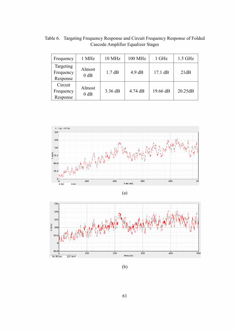
Table 6. Targeting Frequency Response and Circuit Frequency Response of Folded
Cascode Amplifier Equalizer Stages
(a)
(b)
Frequency 1 MHz 10 MHz 100 MHz 1 GHz 1.5 GHz
Targeting
Frequency
Response
Almost
0 dB 1.7 dB 4.9 dB 17.1 dB 21dB
Circuit
Frequency
Response
Almost
0 dB 3.36 dB 4.74 dB 19.66 dB 20.25dB

62
(c)
(d)
(e)
Figure 3.16: Folded Cascode Amplifier Type Equalizer Stage Cascade Results
(a) Input (b) Output of the First Equalizer Stage (c) Output of the Second
Equalizer Stage (d) Output of the Third Equalizer Stage (e) Final Output Eye
Diagram

63
The frequency response at 1 GHz and 1.5 GHz can not be satisfied together due to
the first order filter frequency response slope. The results shown in Figure 3.15 and
Figure 3.16 illustrated the tradeoff between the two scenarios. If the frequency
response at 1 GHz was satisfied, the response at 1.5 GHz had roughly a 2 dB error and
caused a 6 dB attenuation on eye height at the final output. This could be seen in the
simulation result. If the frequency response at 1.5 GHz was satisfied, the frequency
response at 1 GHz was 2 dB higher than needed. This increased the final jitter from
0.2 UI to 0.3 UI, also shown in the simulation result.
Chapter 4. Conclusion and Future Work
In this thesis, a genetic algorithm was used for modeling the coaxial cable
frequency response characteristics, the maximum error was limited within 0.25 dB.
Aiming at a 1080P full HD video signal with 1.5Gbps data rate, an adaptive equalizer
system-level model with QFB block was built and tested by cable models with different
cable lengths. Two circuits based on different amplifiers are implemented in GPDK
45 nm technology, both circuits are working as single adaptive equalizer stages. Two
tuning methods are used and corresponding results are compared. Adaptive ability are
tested and the results are compared with model simulation results. A cascade of three
equalizer stages was tested in the end, two different structures are used and the results
are compared.

64
This work aims to transfer existing BJT and BiCMOS design into CMOS
implementation. Adaptive control mechanism and QFB block is not implemented in
circuit level. Frequency response tuning is still an open problem since jitter and eye
height cannot be optimized together unless decrease the cable length. It will be a
valuable work if an mathematic model about frequency response tuning can be found.
QFB and control block also need to be designed and the complete circuit will be
fabricated and tested.
65
References
[1] Martin J. Van Der Burgt, "Coaxial Cable and Applications,", Belden Electronics
Division.
[2] Shakiba, M.H., "A 2.5 Gb/s Adaptive Cable Equalizer," Solid-State Circuits
Conference, 1999. Digest of Technical Papers. ISSCC. 1999 IEEE International,
pp.396-397, 1999.
[3] Andreea Balteanu, "Coaxial Cable Equalization Techniques at 50-110 Gbps,"
M.S. Thesis, Dept. Elect. Eng., Univ. of Toronto, 2010.
[4] Hao Liu, "Analog Equalizers for High-Speed Wire-Line Data Communications,"
Ph.D. dissertation, Dept. Elect. Eng., Univ. of Texas at Dallas, 2010.
[5] Wiki-pedia, "Jitter," [online]. Available: http://en.wikipedia.org/wiki/Jitter
[6] Wiki-pedia, "Genetic Algorithm," [online]. Available:
http://en.wikipedia.org/wiki/Genetic_algorithm
[7] Narges, S.H.,"An automated design flow for cable equalizer in data
communication systems," M.S. Thesis, Dept. Elect. Eng., Univ. of Toronto,
1999.
[8] Wiki-pedia, "Capacitive Coupling," [online]. Available:
http://en.wikipedia.org/wiki/Capacitive_coupling
[9] B. Razavi, Design of Analog CMOS Integrated Circuits, 1st ed. New York:
McGraw-Hill, 2003.
[10] D.A.Johns,K.Martin.(1997). Advanced Current Mirrors and Opamps [online].
Available: http://ee.sharif.edu/~elec3/06_advanced_opamps.pdf
[11] I.Kim et al. " CMOS Ultrasound Transceiver Chip for High-Resolution
Ultrasonic Imaging Systems," IEEE Transactions on Biomedical and Systems,
vol. 3, no. 5, pp.293-303, October, 2009.
[12] C.F.Liao, S.L.Liu, "A 10Gb/s CMOS Amplifier with 35dB Dynamic Range for
10Gb Ethernet," ISSCC Dig. Tech. Paper, Feb., 2006
66
[13] C.H.Wu, C.S.Liu and S.L.Liu, "A 2GHz CMOS Variable-Gain Amplifier with
50dB Linear-in-Magnitude Controlled Gain Range for 10Gbase-LX4 Ethernet,"
ISSCC Dig. Tech. Paper, pp.484-485, Feb., 2004
[14] F.Krummenacher, N.Joehl, "A 4-MHz CMOS Continuous-Time Filter with
On-Chip Automatic Tuning," IEEE J. Solid-State Circuits, vol. 23, pp.750-758,
June, 1988.

67
Appendix
1. Model of A Single Adaptive Equalizer Stage
68
2. CMOS Folded Cascode Amplifier in GPDK 45 nm
Technology
I_b
ias
NM
0N
M5
PM
7
V_b
ias_tail
NM
1
PM
8
PM
9
V_
bias_
tail
V_b
ias_p
m
V_b
ias_p
tP
M1
0
PM
12
NM
7
V_b
ias_p
t
V_b
ias_p
m
NM
8
NM
9
PM
11
PM
13
V_b
ias_n
mV_b
ias_n
b
PM
15
PM
14
NM
10
NM
11
NM
16
NM
17
NM
34
NM
15
NM
14
PM
20
PM
19
Inp
ut+
Inp
ut-
Ou
tpu
t-O
utp
ut+
V_b
ias_p
t
V_b
ias_p
m
V_b
ias_n
m
V_b
ias_n
b
V_b
ias_tail

69
3. Folded Cascode Amplifier Type Equalizer Stage
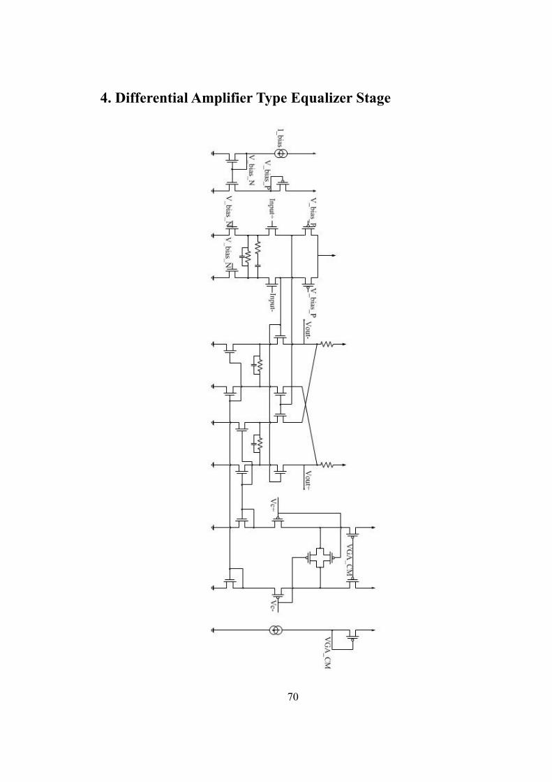
70
4. Differential Amplifier Type Equalizer Stage