System for Acquisition of Corneal Images · System for Acquisition of Corneal Images Slip Lamp...
84
System for Acquisition of Corneal Images Slip Lamp Application Thesis by Hugo José Pinto de Almeida In Fulfillment of the Requirements for Master’s Degree in Biomedical Engineering Coimbra, September 2012 (defended September 24)
Transcript of System for Acquisition of Corneal Images · System for Acquisition of Corneal Images Slip Lamp...

System for Acquisition of Corneal Images Slip Lamp Application
Thesis by
Hugo José Pinto de Almeida
In Fulfillment of the Requirements
for
Master’s Degree in Biomedical Engineering
Coimbra, September 2012
(defended September 24)

This work is funded by FEDER, through the Programa Operacional Factores de Competitividade-COMPETE and by National funds through FCT- Fundação para a Ciência e Tecnologia in the frame of project PTDC/SAU-BEB/104183/2008, F-COMP-01-0124-FEDER-010941
Este trabalho é financiado pelo FEDER, através do Programa Operacional Factores de Competitividade- COMPETE e fundos nacionais através da FCT- Fundação para a Ciência e Tecnologia no âmbito do projeto PTDC/SAU-BEB/104183/2008, F-COMP-01-0124-FEDER-010941

ii
Esta cópia da tese é fornecida na condição de que quem a consulta reconhece que os
direitos de autor são pertença do autor da tese e que nenhuma citação ou informação
obtida a partir dela pode ser publicada sem a referência apropriada.
This copy of the thesis has been supplied on condition that anyone who consults it is
understood to recognize that its copyright rests with its author and that no quotation from
the thesis and no information derived from it may be published without proper
acknowledgement.
All contents written in Portuguese are in compliance with Old Portuguese Language
Orthographic Agreement.

iii
Accepted by the University of Coimbra, in fulfillment of the requirements for the
degree of Master in Biomedical Engineering.
Thesis Examination Committee:
_____________________________________________
(PhD) Custódio Francisco Loureiro Melo1,2 (Chairperson)
_____________________________________________
(PhD) Francisco José Amado Santiago Fernandes Caramelo3
_____________________________________________
(PhD) José Paulo Pires Domingues1,3 (Advisor)
1Department of Physics, Faculty of Sciences and Technology, University of Coimbra, Portugal
2Instrumentation Center, Faculty of Sciences and Technology, University of Coimbra, Portugal
3IBILI – Institute of Biomedical Research in Light and Image, Faculty of Medicine, University of
Coimbra, Portugal

iv
Aos meus pais,
___________________________

v
Acknowledgements Começo por agradecer a toda a equipa do projecto NeuroCórnea, em particular ao
Professor Doutor José Paulo Domingues, meu orientador de projecto, pelo
acompanhamento prestado durante todo o ano.
Agradeço aos meus avós paternos por estarem presentes na minha vida, não só nesta
fase mas no passado e daqui adiante.
Ao Maurício (palmas ao malabarista) e à Carlota (com um beijo), que me
acompanharam de perto durante o decorrer do projecto e a escrita da tese, agradeço pelos
bons momentos.
Aos meus pais, muitíssimo obrigado por todo o esforço e dedicação que possibilitou a
minha caminhada pelo percurso universitário. Esta tese é-lhes dedicada.
A todos, agradeço.

vi
Abstract Diabetes is a chronic disease that is associated chronic complications such as diabetic
neuropathy - leading cause of disability in diabetics.
Currently, corneal confocal microscopy is a technique used to acquire in vivo images of
the cornea nerves. As an expensive technology which is only available in central hospitals
and private clinics, the case of a slit lamp microscope is a starting point to improve this
solution since it is often used to observe the anterior segment of the eye. Thus, the
purpose of NeuroCórnea is (but not only) the development of a confocal module for use in
a slit lamp microscope; a method for assessing the corneal nerves for diagnosis and
monitoring of diabetic neuropathy.
A part of the object of NeuroCórnea has to do light intensity measurement. In order to
achieve part of this goal, has been proposed an acquisition model based on a Hamamatsu
FFT-CCD C5809 Image Sensor and controlled by a PIC microcontroller. Due to a failure that
arose during the project, the FFT-CCD was replaced by a S3921-128Q MOS Linear Image
Sensor, which would be the only way to continue to get results.
During the course of the project we were given the opportunity to work with LIP-
Coimbra (Laboratory of Instrumentation and Experimental Physics of Particles) and
adapting our entire system (hardware, firmware and software) for a temperature
measurement system for a liquid xenon detector. This was not an objective proposed in the
beginning but served to consolidate knowledge and show the versatility of the
instrumentation.
In order to handle all these devices (PIC, FFT-CCD, MOS and LIP circuit) was created a
GUI (Graphical User Interface) using Microsoft Visual Studio C++ that has, among other
features, the ability to view real-time video outputs for each device.
In short, this project was handling a wide range of variables such as: electronic
components (regulators, references, ADC ...), PIC microcontroller, graphical interface (GUI),
C programming language (C and Visual C++), Assembler programming language, handling
various tools (an example is welding with tin). In the end, the knowledge gained was
successful and personally rewarding.
Keywords: Cornea, diabetic neuropathy, FFT-CCD, PIC microcontroller, MOS, LIP.

vii
Resumo
A diabetes é uma doença crónica que tem associadas complicações como por exemplo
a neuropatia diabética – maior causa de incapacidade em diabéticos.
Actualmente, a microscopia confocal da córnea é a técnica usada para adquirir imagens
dos nervos da córnea in vivo. Sendo uma tecnologia onerosa e que só está disponível em
hospitais centrais e clínicas privadas, o caso do microscópio de lâmpada de fenda é um
ponto de partida para melhorar esta solução uma vez que é frequentemente usado para
observar o segmento anterior do olho humano. Assim, o propósito da NeuroCórnea é (mas
não só) o desenvolvimento de um módulo confocal para aplicação num microscópio de
lâmpada de fenda. É um método para avaliação dos nervos da córnea, para o diagnóstico e
acompanhamento da neuropatia diabética.
Uma parte do objectivo da NeuroCórnea tem que ver com a medição da intensidade.
De modo a cumprir uma parte deste objectivo foi proposto um modelo de aquisição
baseado num sensor de imagem FFT-CCD C5809 da Hamamatsu e comandado por um
microcontrolador PIC. Devido a uma avaria que surgiu no decorrer do projecto, o sensor
FFT-CCD foi trocado por um sensor de imagem linear S3921-128Q MOS, que seria o único
modo de prosseguir para obter resultados.
Durante o decorrer o projecto foi-nos dado a oportunidade de trabalhar com o LIP-
Coimbra (Laboratory of Instrumentation and Experimental Physics of Particles) num
sistema de medição de temperatura para uma câmara de xénon líquido e, adaptando todo
o nosso sistema (hardware, firmware e software), conseguimos atingir o objectivo
proposto. Este não era um objectivo proposto no início mas serviu para consolidar
conhecimentos e mostrar a versatilidade da instrumentação.
De modo a manipular todos estes dispositivos (PIC, FFT-CCD, MOS e circuito do LIP) foi
criada uma interface gráfica usando o Microsoft Visual Studio C++ que tem, entre outras
funcionalidades, capacidade de visualizar em tempo real as saídas vídeo de cada
dispositivo.
Em suma, neste projecto houve manipulação de uma pluralidade de variáveis tais
como: componentes electrónicos (reguladores, referências, ADC...), microcontroladores
PIC, linguagens de programação C (Visual C++ e C), interface gráfica, linguagem de
programação Assembler, manuseamento de vários instrumentos (um exemplo é a
soldadura com estanho)... No fim, a aprendizagem obtida foi pessoalmente gratificante.
Palavras-chave: Córnea, neuropatia diabética, FFT-CCD, microcontrolador PIC, MOS,
LIP.

viii
Table of Contents
Acknowledgements ............................................................................................................................... v
Abstract ................................................................................................................................................ vi
Resumo ............................................................................................................................................... vii
Table of Contents ............................................................................................................................... viii
List of Figures ....................................................................................................................................... xi
List of Tables ........................................................................................................................................ xii
List of Examples ................................................................................................................................... xii
Chapter 1. Introduction ................................................................................................................ 1-1
1.1 - Diabetic Neuropathy ........................................................................................................ 1-1
1.2 - NeuroCórnea .................................................................................................................... 1-1
1.3 - Objective .......................................................................................................................... 1-2
1.4 - Microcontrollers ............................................................................................................... 1-2 1.4.1 - PIC ............................................................................................................................. 1-3
1.5 - Von Neumann Architecture ............................................................................................. 1-4
1.6 - Harvard Architecture ....................................................................................................... 1-4
1.7 - Modified Von Neumann Architecture and Harvard Architecture..................................... 1-5
Chapter 2. PIC32 USB Starter Kit II Microchip .............................................................................. 2-1
2.1 - PIC32MX (PIC32MX795F512L) ......................................................................................... 2-2 2.1.1 - Interrupts .................................................................................................................. 2-2
2.1.1.1 - Interrupt Priorities and Sub Priorities ............................................................... 2-2 2.1.2 - I/O Ports ................................................................................................................... 2-3
2.1.2.1 - Control Registers ............................................................................................... 2-3 2.1.2.2 - Modes of Operation .......................................................................................... 2-3
2.1.3 - Timers ....................................................................................................................... 2-4 2.1.3.1 - Control Registers ............................................................................................... 2-4 2.1.3.2 - Interrupt Configuration ..................................................................................... 2-5
2.1.4 - Output Compare ....................................................................................................... 2-5 2.1.4.1 - Output Compare Functions ............................................................................... 2-6
2.2 - I/O Expansion Board ........................................................................................................ 2-8
Chapter 3. Power Supply Voltage Board ...................................................................................... 3-1
3.1 - PT78NR115S (-15V) .......................................................................................................... 3-2
3.2 - L7812CV (+12V)................................................................................................................ 3-2
3.3 - LM7815CV (+15V) ............................................................................................................ 3-2
3.4 - LM78M05CT (+5V) ........................................................................................................... 3-3
3.5 - LD1085V50 (+5V) ............................................................................................................. 3-3
3.6 - IE1224S (+24V) ................................................................................................................. 3-4

ix
3.8 - PTN78000A (-15V) ........................................................................................................... 3-5
3.7 - REF 195 ............................................................................................................................ 3-5
3.8 - 16-bit ADC AD7680 .......................................................................................................... 3-6
Chapter 4. Hamamatsu Image Sensors ........................................................................................ 4-1
4.1 - FFT-CCD C5809 Image sensor .......................................................................................... 4-1 4.1.1 - Timing signal generator ............................................................................................ 4-1 4.1.2 - Voltage regulators .................................................................................................... 4-1 4.1.3 - Inputting the control signal from the PIC (Start and CLK) ........................................ 4-2
4.2 - S3921-128Q MOS Linear Image Sensor ........................................................................... 4-2 4.2.1 - Driver Circuit ............................................................................................................. 4-2 4.2.1 - Signal Readout Circuit .............................................................................................. 4-3
Chapter 5. Temperature Monitor for a Liquid Xenon Detector ................................................... 5-1
5.1 - LIP - Laboratory of Instrumentation and Experimental Physics of Particles .................... 5-1
5.2 - 1N4148 diodes ................................................................................................................. 5-1 5.2.1 – Specifications ........................................................................................................... 5-2
5.3 - PCB ................................................................................................................................... 5-2
5.4 – LIP circuit ......................................................................................................................... 5-3
Chapter 6. Firmware ..................................................................................................................... 6-1
6.1 - Introducing MPLAB .......................................................................................................... 6-1
6.2 - The elements of MPLAB ................................................................................................... 6-1
6.3 - MPLAB C32 C Compiler .................................................................................................... 6-2 6.3.1 - File Naming Conventions .......................................................................................... 6-2 6.3.1.1 - Data Storage .......................................................................................................... 6-2
Storage Endianness ......................................................................................................... 6-2 Integer Representation ................................................................................................... 6-2 Signed and Unsigned Character Types ............................................................................ 6-3 Floating-Point Representation ........................................................................................ 6-3
6.3.2 - Pragmas (pragmatic information) ............................................................................ 6-3 6.3.3 - Interrupts .................................................................................................................. 6-4
Chapter 7. Software...................................................................................................................... 7-1
7.1 - Visual C++/CLI .................................................................................................................. 7-1 7.1.1 - .NET .......................................................................................................................... 7-1 7.1.2 - Framework .NET ....................................................................................................... 7-2 7.1.3 - Common Language Runtime .................................................................................... 7-2
7.2 - Windows Forms ............................................................................................................... 7-3
Chapter 8. Results......................................................................................................................... 8-1
8.1 - The graphical interface (GUI) ........................................................................................... 8-1 8.1.1- Communication between Forms ............................................................................... 8-1
8.2 - Data Visualization ............................................................................................................ 8-2 8.2.1 - Save data in .txt format. ........................................................................................... 8-2
8.3 - Communication between PC and PIC ............................................................................... 8-3 8.3.1 - Sending Data to PIC Firmware .................................................................................. 8-3 8.3.2 - Sending Data to PC Software .................................................................................... 8-4
9.3.2.1 - How conversions are made ............................................................................... 8-5

x
8.4 - ADC Tests ......................................................................................................................... 8-6 8.4.1 - Effective number of bits (ENOB) of the 16-bit ADC AD7680 .................................... 8-6
8.1.1.1 - 1.3 Volts battery test......................................................................................... 8-7 8.4.2 - ADC units to Volts conversion .................................................................................. 8-8 8.4.3 - SPI communication ................................................................................................... 8-9
8.5 - FFT-CCD image sensor ................................................................................................... 8-10 8.5.1 - External control signals .......................................................................................... 8-10 8.5.2 - Acquisition parameters .......................................................................................... 8-11 8.5.3 - Disk storage ............................................................................................................ 8-12 8.5.4 - Processing of Data .................................................................................................. 8-13
8.6 - LIP – Temperature Monitor for Liquid Xenon Detector .................................................. 8-13
8.7 - MOS Linear Image Sensor .............................................................................................. 8-15 8.7.1 - External control signals .......................................................................................... 8-15 8.7.2 - A/D Conversion....................................................................................................... 8-16 8.7.3 - Pixel duration time ................................................................................................. 8-16
8.8 - Final prototype ............................................................................................................... 8-17
8.9 - Unsolved problems ........................................................................................................ 8-18
Chapter 9. Conclusion and Future work ....................................................................................... 9-1
Bibliography ........................................................................................................................................... I
Attachment I ......................................................................................................................................... A
Attachment II ........................................................................................................................................ B
Attachment III ....................................................................................................................................... C
Attachment IV ...................................................................................................................................... D
Attachment V ........................................................................................................................................ E
Attachment VI ....................................................................................................................................... F
Attachment VII ..................................................................................................................................... G
Attachment VIII .................................................................................................................................... H
Attachment IX ........................................................................................................................................ I
Attachment X ......................................................................................................................................... J
Attachment XI ....................................................................................................................................... K
Attachment XII ...................................................................................................................................... L
Attachment XIII ....................................................................................................................................M
Attachment XIV .................................................................................................................................... N

xi
List of Figures
Figure 1-1. Zilog Z80 - 8-bit microprocessor designed and sold by Zilog from July 1976. [7] ______ 1-2 Figure 1-2. The Von Neumann architecture. [10] ________________________________________ 1-4 Figure 1-3. The Harvard architecture. [10] _____________________________________________ 1-5 Figure 2-1. PIC32 USB Starter Kit II. [13] _______________________________________________ 2-1 Figure 2-2. Interrupt Controller Module._______________________________________________ 2-2 Figure 2-3. The Starter Kit I/O Expansion Board.[14] _____________________________________ 2-8 Figure 2-4. Microchip PICtail Plus Daughter Board. ______________________________________ 2-8 Figure 3-1. Board with power supplies for the Hamamatsu FFT-CCD C5809 Image Sensor _______ 3-1 Figure 3-2. Standart Application, Pin-Out Information and Ordering Information of PT78NR100
Series. [16] __________________________________________________________________ 3-2 Figure 3-3. Connection Diagram (top view) and Standart Application Circuits of the L7800 series
regulators.[17] _______________________________________________________________ 3-2 Figure 3-4. Connection Diagram (top view) and Standart Application Circuits of the LM7800 series
regulators.[18] _______________________________________________________________ 3-3 Figure 3-5. Connection Diagram of the LM78M05CT regulator.[19] _________________________ 3-3 Figure 3-6. Pin Configuration (top view) and Application Circuit of the LD1085V50 regulator.[20] _ 3-4 Figure 3-7. Image and pinout of IE1224S DC/DC Converter.[21] ____________________________ 3-4 Figure 3-8. Standard Application of PTN78000A regulator. Application Information in Attachment
V.[23] ______________________________________________________________________ 3-5 Figure 3-9. Typical Connection Diagram of the REF195. [22] _______________________________ 3-5 Figure 3-10. Functional Block Diagram and Pin Configuration of 16-Bit AD7680. [22] ___________ 3-6 Figure 4-1. Timing diagram for drive circuit of S3921-128Q MOS Linear Image Sensor [28]. ______ 4-3 Figure 4-2. Recommend readout circuit and pulse timing for S3921-128Q MOS Linear Image
Sensor.[28] __________________________________________________________________ 4-4 Figure 4-3. Header for communication between MOS and PIC._____________________________ 4-4 Figure 5-1. PCB used to measure the temperature of the D1 and D2 diodes. __________________ 5-2 Figure 5-2. Schematic of the circuit that will monitor the temperature of a liquid xenon detector. 5-3 Figure 7-1. Framework .NET architecture diagram. ______________________________________ 7-1 Figure 7-2. Image of the first Form of the graphical user interface (GUI). _____________________ 7-3 Figure 8-1. Communication between two Windows Forms ________________________________ 8-1 Figure 8-2. ADC WindowsForm image where the ADC parameters are selected. _______________ 8-6 Figure 8-3. .txt file that demonstrates a slight increase of values of SCAN NUMBER: 3 in relation to
the SCAN NUMBER: 2. _________________________________________________________ 8-8 Figure 8-4. Scheme of ADC units to Volt conversion. _____________________________________ 8-8 Figure 8-5. Microchip PICtail Plus Daughter Board with components. _______________________ 8-9 Figure 8-6. Schematic of the correspondence between ADC pins and PIC pins. ________________ 8-9 Figure 8-7. Header (in PIC daughter board) for connecting the Start and Clock signals FFT-CCD image
sensor and for connection of Trigger signal to the PIC. ______________________________ 8-10 Figure 8-8. FFT-CCD image sensor 15-pin D-SUB Connector. ______________________________ 8-11 Figure 8-9. Picture of the selection window of FFT-CCD parameters. _______________________ 8-12 Figure 8-10. Scheme illustrating the 1 Hz square wave used as a trigger to synchronize conversions of
diode D1 and diode D2. _______________________________________________________ 8-13 Figure 8-11. File in ASCII format which are stored the mean values and standard deviation of each D1
and D2 conversion. __________________________________________________________ 8-14 Figure 8-12. Picture of the GUI where we can view D1 and D2 variations. ___________________ 8-14 Figure 8-13. Graphs of temperature variation in diodes D1 and D2. These graphs were obtained using
an excel sheet. ______________________________________________________________ 8-15 Figure 8-14. Header (in PIC daughter board) with all signals for MOS sensor. ________________ 8-15 Figure 8-15. Video output of S3921-128Q MOS linear image sensor in the oscilloscope and
conversions to be made. ______________________________________________________ 8-16

xii
Figure 8-16. An acquisition of MOS. _________________________________________________ 8-17 Figure 8-17. Final prototype with MOS. ______________________________________________ 8-17 Figure 8-18. Schematic with state buffer/line driver (ex.: HCT244). ________________________ 8-19 Figure M-1. AD7680 Serial Interface Timing Diagram - 24SCLK Transfer. ______________________ M Figure M-2. AD7680 Serial Interface Timing Diagram - 20 SCLK Transfer. ______________________ M
List of Tables
Table 3-1. LM78M05CT Specifications.[19] ......................................................................................... 3-3 Table 3-2. Electrical characteristics of LD1085V50.[20] ...................................................................... 3-4 Table 3-3. Input and Output specifications of IE1224S DC/DC Converter.[21] ................................... 3-4 Table 3-4. Terminal functions of PTN78000A regulator.[23] .............................................................. 3-5 Table 3-5. Pin Function Descriptions of AD7680. [22] ......................................................................... 3-6 Table 6-1. File extensions names in compilation driver. ..................................................................... 6-2 Table 6-2. Example of stored at address 0x100 of 32-bit value 0x12345678. .................................... 6-2 Table 6-3. Integer representation values in MPLAB C32 C Compiler. ................................................. 6-3 Table 6-4. MPLAB C32 C Compiler floating-point format. ................................................................... 6-3 Table 8-1. Analysis of points converted by the ADC subjected to a potential of 1.3 volts. ................. 8-7 Table 8-2. Analysis of one acquisition with 512 points, converted by the ADC subjected to a potential
of 1.3 volts. ................................................................................................................................. 8-7
List of Examples Example 2-1. Code example will set group priority level. ................................................................... 2-2 Example 2-2. Code example will set group sub priority level.............................................................. 2-3 Example 2-3. Code Example of Analog and digital inputs/outputs. .................................................... 2-4 Example 2-4. 16-Bit Timer Interrupt Initialization Code Example. ...................................................... 2-5 Example 2-5. Timer ISR Code Example. ............................................................................................... 2-5 Example 2-6. Example code for configuration of the single output pulse event and Interrupt Servicing
(16-Bit Mode). ............................................................................................................................ 2-6 Example 2-7. Example code for configuration of the continuous output pulse event and Interrupt
Servicing (16-Bit Mode). ............................................................................................................. 2-6 Example 8-1. Code for communication between two Windows Forms .............................................. 8-1 Example 8-2. Partial code to display data in continuous mode. ......................................................... 8-2 Example 8-3. Partial code for storage in .txt format. .......................................................................... 8-3 Example 8-4. Partial code that shows how values of parameters are sent to the PIC. ....................... 8-4 Example 8-5. Partial code of MPLAB Firmware. .................................................................................. 8-4 Example 8-6. Partial code used to send 512 conversions to PC. ......................................................... 8-5 Example 8-7. Partial code used to make ADC conversions ................................................................. 8-5 Example 8-8.Example of PIC problem description. ........................................................................... 8-19

1-1
Chapter 1. Introduction
1.1 - Diabetic Neuropathy
Diabetic peripheral neuropathy (DPN) is nerve damage caused by diabetes, affects up
to 50% of older type 2 diabetic patients and is the major cause of chronic disability in
diabetic patients, being implicated in 50-75% of non-traumatic amputations. Patients with
peripheral neuropathy must be considered at risk of insensate foot ulceration and must
receive preventive education and care. [1]
The present approach to reduce diabetic neuropathy complications is based on its early
diagnosis and accurate assessment, a difficult task due to the non-availability of a simple
non-invasive method for early diagnosis. [2]
DPN is by far the most common of all the neuropathies and may be divided into the
following two main types:
Acute sensory neuropathy
Chronic sensorimotor neuropathy
Acute sensory neuropathy is a distinct variety of the symmetrical polyneuropathies1
with an acute or sub-acute onset characterized by severe sensory symptoms, usually with
few if any clinical signs.
Chronic sensorimotor neuropathy is by far the most common form of DPN. It’s usually
of insidious onset and may be present at the diagnosis of type 2 diabetics in up to 10% of
patients. Whereas up to 50% of patients with chronic DPN may be asymptomatic symptoms
sufficient to warrant specific therapy. [3]
Management of diabetic neuropathy includes two approaches: therapies for
symptomatic relief and those that may slow the progression of neuropathy. Of all
treatments, tight and stable glycemic control is probably the most important for slowing
the progression of neuropathy. [4]
The cornea is one of the most densely innervated tissues in the human body and is
accessible to inspection through optical methods. In the past 15 years, several researches
proposed the use of morphologic parameters extracted from images of the corneal sub-
basal nerve plexus, acquired in vivo, on conscious patients, using corneal confocal
microscopy (CCM). [5]
1.2 - NeuroCórnea
The NeuroCórnea has the purpose of early detection and monitoring of diabetic
peripheral neuropathy by automatic analysis of the in vivo morphology of corneal sub-basal
nerves. The technique will be based on dedicated instrumentation meant to be coupled to
1 Poluneuropathy is a neurological disorder that occurs when many nerves throughout the body
malfunction simultaneously.

1-2
a standard slip lamp, a feature that will ease its adaptation by ophthalmologists and
general practitioners. [5,6]
This thesis project has an application in respect of NeuroCórnea. It is therefore
requested a construction of a system capable of measuring the density of light from a slit
lamp.
1.3 - Objective
This is a continuing project, initiated in 2010/2011, and aims to consolidate
conceptually a prototype system to acquire/scan based on a PIC microcontroller and a USB
interface. The goal is also the control with speed and resolution suitable for the acquisition
of confocal images of the cornea provided by a camera attached to a slip lamp.
The aims to embody the following tasks:
1. Study the existing system and its main components
2. Survey of possible operational problems and limitations
3. Digital oscilloscope. Acquisition in real time (continuously)
4. Submission of a comprehensive proposal for implementation of the final
prototype
5. Completing the hardware/firmware solution and implementation of graphical
user interface (GUI) for the acquisition and control
6. Image acquisition and parameterization of the performance in terms of
resolution, speed and sensitivity
7. Adaptation of firmware and software to other applications
1.4 - Microcontrollers
Microcontrollers are smart chips, which has a processor, pin for input/output (I/O) and
memory. By programming the microcontroller can control their output, with reference
inputs or an internal program.
What differentiates the various types of microcontrollers is the amount of memory
(program and data), processing speed, number of I/O pins, power, peripherals, architecture
and instruction set.
First to all we need to differentiate a microcontroller of a microprocessor, easy terms
to be confused but there is great difference between them.
Figure 1-1. Zilog Z80 - 8-bit microprocessor designed and sold by Zilog from July 1976. [7]

1-3
A microprocessor circuit is very complex, in the form of an integrated circuit, which can
contain from a few thousand (Figure 1-1) to 7 million transistors (Pentium II). These
transistors are the most diverse internal logic circuits, such as counters, registers, decoders
and hundreds of others. These logic circuits are arranged in a complex manner, giving the
microprocessor the ability to perform logical, arithmetic and control operations.[7]
A microcontroller is na integrated circuit that has na internal microprocessor and all
peripherals essential to its operation, like:
Program Memory – usually an EPROM1 type memory which stores the program
information, ie, the microprocessor should execute.
Data Memory – usually a type memory RAM (Random Acess Memory), where
the information will be stored data that the program will use, is usually used to
store a value or a flag.
I/O Device Selection – is the communication of memory locations with the
external pins of the microcontroller.
Timers and Counters – used to tell time or count events.
Clock – in some microcontrollers the clock signal generator is also coupled to
the microprocessor, it has the function to synchronize all the events of a digital
circuit.
Interrupt Controller Device – as the name implies, is the component that
controls the interrupt request to the CPU.
1.4.1 - PIC
PIC (Peripheral Interface Controller) is a family of microcontrollers manufactured by
Microchip Technology® which process data of 8-bits, 16-bits and more recently 32-bits (our
case). They have wide variety of models and internal peripherals, have high processing
speed due to its Harvard architecture and RISC2 instruction set (35 sets of instructions and
76 instructions), with resources for programming flash memory and EEPROM3. (See
Chapter 2)
Note.: The PIC18F also process data of 32-bit, double type variables for example. What
distinguishes the architectures is the ALU4. In the PIC18 is 8bits, in the PIC24 16bit ALU and
have a PIC32 32-bit ALU
1 EPROM (rarely EROM), or Erasable Programmable Read Only Memory is a type of memory chip
that retains its data when its power supply is switched off. In other words, it is non-volatile. 2 RISC or Reduced Instruction Set Computer simplifies the processor by only implementing
instructions that are frequently used in programs; unusual operations are implemented as subroutines, where the extra processor execution time is offset by their rare use.
3 EEPROM (also written E2PROM) stands for Electrically Erasable Programmable Read-Only
Memory and is a type of non-volatile memory used in computers and other electronic devices. 4 Arithmetic and Logic Unit (ALU) is a digital circuit that performs arithmetic and logical
operations.

1-4
1.5 - Von Neumann Architecture
The Architecture of Von Neumann (Figure 1-2) is a computer architecture that is
characterized by the possibility of a digital machine to store your programs on the same
memory space as the data, thus being able to handle such programs. [8]
The Von Neumann architecture is used in microprocessor instructions which may have
different formats, ie, the number of bytes used for writing the instructions may vary for
instruction statement, and therefore, these microprocessors allows the use of a broad
range instruction. CPUs are CISC (Complex Instruction Set Computer), suitable for software
development highly structured and based on the use of repertoires of instructions that
allows great design flexibility. [9]
Figure 1-2. The Von Neumann architecture. [10]
1.6 - Harvard Architecture
The Harvard Architecture (Figure 1-3) based on a concept that the latest Von Neumann,
and has been the need for the microcontroller to work faster. It’s a computer architecture
that distinguishes itself from others by having two different and independent memories in
terms of bus and connection to the processor. It’s based on the separation of bus and
connection which are memories of the program instructions and data memories, allowing a
processor can access both simultaneously, obtaining a better performance than the Von
Neumann architecture, it may seek a new instructions while executing another. [11]
The Harvard Architecture is particularly suited for microprocessors that, by using a
reduced number of instructions, are usually designated by RISC (Reduced Instruction Set
Computer). [9]
Our PIC microcontroller family, which will be further specified in more detail, displays
Harvard architecture and is designed in light of the RISC philosophy. For example,
processors PIC16Fxxxx use a repertoire of thirty-five instructions written with words of
fourteen bits, and operate on data words of eight bits.

1-5
Figure 1-3. The Harvard architecture. [10]
1.7 - Modified Von Neumann Architecture and Harvard Architecture
Before closing this chapter, it should be noted that the distinction of slides based on
the concept of philosophies CISC and RISC, or classification of the architecture, such as
Harvard or Von Neumann, tends to blur as manufacturers of microprocessors increasingly
betting more on developing devices whose architecture does not fit precisely those
concepts. Often, these constructs are called "Modified Von Neumann Architecture" or
"Modified Harvard Architecture" and display a repertoire of these microprocessors,
instruction reinforced, ie a repertoire that, in addition to containing instructions, comprises
instructions to a large processing capacity. [9]
For example, in some microcontrollers and in many microprocessors - signal processors
of the type DSP (Digital Signal Processor) - often using a Modified Harvard Architecture, to
allow the transfer of operands through the bus, at the outset, is dedicated to the program
memory access, thus improving the performance of systems to perform operations on two
operands that are involved.

2-1
Chapter 2. PIC32 USB Starter Kit II Microchip
The PIC32 USB Starter Kit II (Figure 2-1) provides a method to experience the USB
functionality of the PIC32 microcontroller. We can develop CAN (Controller Area Network)
applications using PIC32 expansion board. With the board we can develop USB embedded
host/device/OTG (USB On-The-Go) applications because it’s possible combining this board
with Microchip’s free USB software. [12]
PIC32 USB Starter Kit II includes the following items:
PIC32 USB Starter Kit II Development Board
USB mini-B to full-sized A cable for debug.
USB micro-B to full-sized A cable to communicate with the PIC32 USB port
Three user-programmable LEDS
Three push button switches
Figure 2-1. PIC32 USB Starter Kit II. [13]
Note.: The content (Figures and Examples) which are presented below, was adapted
from “PIC32MX Family Reference Manual”, for this reason there will be no other reference
in this section (Chapter 2.1). This document is available on a CD-ROM that accompanies the
PIC32 USB Starter Kit II and is available online on Microchip website. The intension of its
inclusion was to provide the reader overall information of this important content for work
project.

2-2
2.1 - PIC32MX (PIC32MX795F512L)
The PIC32MX795F512L manipulation involves a huge knowledge of its architecture, its
functional blocks and their components. There is no logic to explain everything about the
PIC in this thesis; however, I will make a brief reference to the functional blocks of most
interest.
2.1.1 - Interrupts
In response to interrupt events, PIC32MX795F512L generates interrupt request. The
interrupts module includes the following (but not only) features:
96 interrupt sources
64 interrupt vectors
Single and Multi-Vector mode operations
7 user-selectable priority levels for each vector
4 user-selectable sub priority levels within each priority
Figure 2-2. Interrupt Controller Module.
Note.: The Attachment I provide a brief summary of interrupt module registers.
2.1.1.1 - Interrupt Priorities and Sub Priorities
We can select priority levels in range from 1 (low) to 7 (high). If an interrupt priority is
“0”, the interrupt vector is disabled.
The following code example will set the priority to level 2.
Example 2-1. Code example will set group priority level.

2-3
We can select a sub priority in range from 0 (low) to 3 (high). The following code
example will set the sub priority to level2.
Example 2-2. Code example will set group sub priority level.
2.1.2 - I/O Ports
I/O pins are considered the simplest of peripherals because. I/O pins allow monitor and
control devices.
2.1.2.1 - Control Registers
The I/O Ports module consists of the following Special Function Registers (SFRs):
TRISx: Data Direction register for the module “x”
PORTx: PORT register for the module “x”
LATx: Latch register for the module “x”
ODCx: Open-Drain Control register for the module “x”
Note1.: “x” denotes any port module instances
Note2.: The Attachment II provides a brief summary of all I/O ports-related registers.
2.1.2.2 - Modes of Operation
I/O pins can be configured as:
Digital Inputs (TRIS register bits = 1) Analog Inputs Digital Outputs (TRIS register bits = 0) Analog Outputs Open-Drain Configuration (ODCx register = 1)
Example 2-3 illustrates configuring RB0, RB1 as analog (default) inputs, RB2 as a digital
input and RB4 as a digital output with open-drain enabled using SET, CLR atomic SFR
registers.

2-4
Example 2-3. Code Example of Analog and digital inputs/outputs.
Note.: The Attachment III provides a summary of I/O pin mode settings configuration.
2.1.3 - Timers
We can configure PIC32MX795F512L with two different types of timers:
Type A Timer
16-bit time
Software selectable prescalers 1:1, 1:8, 1:64 and 1:256
Type B Timer
16-bit or 32-bit timer
Software selectable prescalers 1:1, 1:2, 1:4, 1:8, 1:16, 1:32, 1:64 and
1:256
Note.: 32-bit timer/counter configuration requires an even-numbered timer combined
with an adjacent odd-numbered timer, e.g., Timer2 and Timer3, or Timer4 and Timer 5.
2.1.3.1 - Control Registers
We configure a 16-bit timer with the following Special Function Registers (SFRs):
TxCON: 16-Bit Control Register Associated with the Timer
TMRx: 16-Bit Timer Count Register
PRx: 16-Bit Period Register Associated with the Timer
TxIE: Interrupt Enable Control Bit
TxIF: Interrupt Flag Status Bit
TxIP: Interrupt Priority Control Bits
TxIS: Interrupt Subpriority Control Bits
Note.: The Attachment IV summarizes all Timer-related registers.

2-5
2.1.3.2 - Interrupt Configuration
PIC32MX795F512L timer module has an interrupt flag bit TxIF, an interrupt mask bit
TxIE and its priority level.
Example 2-4 will enable Timer2 interrupts, load the Timer2 Period register and starts
the Timer. When a Timer2 period match interrupts occurs, the ISR must clear the Timer2
interrupt status flag in software.
Example 2-4. 16-Bit Timer Interrupt Initialization Code Example.
Example 2-5 demonstrates a simple ISR for Timer1 interrupts. The code at this ISR
handler should perform any application specific operations and must clear the
corresponding Timer1 interrupt status flag before exiting.
Example 2-5. Timer ISR Code Example.
2.1.4 - Output Compare
PIC32MX795F512L output compare (OC) module is used to generate one single pulse or
set of pulses.
Example 2-6 will set the OC1 module for interrupts on the single pulse event and select
Timer2 as the clock source for the compare time base. Example 2-7 set the OC1 for
continuous pulse event.

2-6
Example 2-6. Example code for configuration of the single output pulse event and Interrupt Servicing
(16-Bit Mode).
Example 2-7. Example code for configuration of the continuous output pulse event and Interrupt
Servicing (16-Bit Mode).
2.1.4.1 - Output Compare Functions
This section contains a list of individual functions for Output Compare module and an
example of use of the functions.
CloseOC1 . . . CloseOC5
This function disables the Output Compare interrupt and then turns off the module.
The Interrupt Flag bit is also cleared.

2-7
Code Example: CloseOC1();
ConfigIntOC1 . . . ConfigIntOC5
This function clears the Interrupt Flag bit and then sets the interrupt priority and
enables/disables the interrupt.
Interrupt enable/disable:
OC_INT_ON
OC_INT_OFF
Interrupt Priority:
OC_INT_PRIOR_0 . . . OC_INT_PRIOR_7
Interrupt Sub-priority:
OC_INT_SUB_PRIOR_0 . . . OC_INT_SUB_PRIOR_3
Code Example: ConfigIntOC1(OC_INT_ON | OC_INT_PRIOR_2 | OC_INT_SUB_PRIOR_2);
OpenOC1 . . OpenOC5
This function configures the Output Compare Module Control register (OCxCON) with
the following parameters: Clock select, mode of operation, operation in Idle mode. It also
configures the OCxRS and OCxR registers.
Module on/off control:
OC_ON
OC_OFF
Clock select:
OC_TIMER2_SRC
OC_TIMER3_SRC
Output Compare modes of operation:
OC_PWM_FAULT_PIN_ENABLE
OC_PWM_FAULT_PIN_DISABLE
OC_CONTINUE_PULSE
OC_SINGLE_PULSE
OC_TOGGLE_PULSE
OC_HIGH_LOW
OC_LOW_HIGH
OC_MODE_OFF

2-8
Code Example: OpenOC1(OC_ON | OC_TIMER2_SRC | OC_PWM_FAULT_PIN_ENABLE,
0x80, 0x60);
2.2 - I/O Expansion Board
The Starter Kit I/O Expansion Board provides full access to MCU signals, additional
debug headers and connections of PICtail™ Plus daughters boards. MCU signals are
available to attaching prototype circuits or monitoring signals with logic probes. [14]
Figure 2-3. The Starter Kit I/O Expansion Board.[14]
To make the connections of external devices to the PIC we use a daughter board to
solder the wires and devices required. The advantage of having a daughter board is its
portability, ie, it is not necessary to remove the PIC development board for soldering wires,
another advantage is that perhaps if something goes wrong, we know that all connections
are being made to from the daughter board, so it is easier to discover the provenance of
the breakdown.
Figure 2-4. Microchip PICtail Plus Daughter Board.
Note.: The pin out equivalence of the development board for the daughter board is
shown in Attachment XI.

3-1
Chapter 3. Power Supply Voltage Board The power board in Figure 3-1 was built entirely by us. This board has the function to
supply all components of our system and has two power inputs (1 and 2).
This board also has an ADC and communication with PIC is made by SPI. (See
Attachment XIII)
Figure 3-1. Board with power supplies for the Hamamatsu FFT-CCD C5809 Image Sensor
Legend of Figure 3-1:
1 - XP Power, model AED100US19 that provides +19 V DC output of power (Input)
2 - ELECTRO DH, model 50.055 that provides +6.5V DC output of power (Input)
3 -GND
4 - +5V (PIC supply)
5 - GND, +5, +15, -15, +24 Volts (Output)
6 - 16-bit ADC AD7680
Note.: 6.5 V input is required for LD1085V50 regulator because dropout is guaranteed
at a maximum of 1.2 V at the maximum output current. Experimentally it was found that
when we supply the regulator with 19V, 15V or 12V it was very hot and damaged.
Moreover, we needed current of about 2A to the FFT-CCD and we could not maintain the
5V regulator.

3-2
3.1 - PT78NR115S (-15V)
The PT78NR115S (Figure 3-2) creates a negative output voltage (-15V) from a 12V of
input voltage with maximum output power of 5 watts. [16]
Figure 3-2. Standart Application, Pin-Out Information and Ordering Information of PT78NR100 Series.
[16]
3.2 - L7812CV (+12V)
The L7812CV of three-terminal positive regulator (Figure 3-3) creates a positive output
voltage (+12V) from a +19V of input voltage and can deliver over 1A output current. [17]
Figure 3-3. Connection Diagram (top view) and Standart Application Circuits of the L7800 series
regulators.[17]
3.3 - LM7815CV (+15V)
The LM7815CV is available in an aluminum TO-31 package (Figure 3-4) which will allow
over 1.0A load current if adequate heat sinking is provided and creates a positive output
voltage (+15V) from +12 of input voltage. [18]
1 TO-3 (“transistor outline”) is a designation for a standardized metal semiconductor package
used for transistors and some integrated circuits.

3-3
Figure 3-4. Connection Diagram (top view) and Standart Application Circuits of the LM7800 series
regulators.[18]
3.4 - LM78M05CT (+5V)
The LM78M05CT of three-terminal positive voltage regulator (Figure 3-5) creates a
positive output voltage (+5V) from positive input voltage [19]
Figure 3-5. Connection Diagram of the LM78M05CT regulator.[19]
Table 3-1. LM78M05CT Specifications.[19]
3.5 - LD1085V50 (+5V)
The LD1085V50 is a low drop voltage regulator (Figure 3-6) able to provide up to 3 A of
output current. Dropout is guaranteed at a maximum of 1.2 V at the maximum output
current, decreasing at lower loads. Only a 10 μF minimum capacitor is need for stability and
creates a positive output voltage (+5V) from ELECTRO DH, model 50.055 that provides
+6.5V DC output. [20]

3-4
Figure 3-6. Pin Configuration (top view) and Application Circuit of the LD1085V50 regulator.[20]
Table 3-2. Electrical characteristics of LD1085V50.[20]
3.6 - IE1224S (+24V)
The IE1224S reference provides +24V DC output from +12V input voltage.
Figure 3-7. Image and pinout of IE1224S DC/DC Converter.[21]
Table 3-3. Input and Output specifications of IE1224S DC/DC Converter.[21]

3-5
3.8 - PTN78000A (-15V)
This component was used in place of the PT78NR115S (there is no longer for sale).
Operating from a wide-input voltage range, the PTN78000A provides high-efficiency,
positive-to-negative voltage conversion for loads of up to 1.5 A. The output voltage is set
using a single external resistor, and may be set to any value within the range, –15V to –3V
(Table 3-4). [23]
Figure 3-8. Standard Application of PTN78000A regulator. Application Information in Attachment V.[23]
Table 3-4. Terminal functions of PTN78000A regulator.[23]
3.7 - REF 195
In fact, because the supply current required by the 16-bit AD7680 is so low, a precision
reference can be used as the supply source to the AD7680. REF195 (Figure 3-9) can be used
to supply the required voltage to the ADC AD7680. This configuration is especially useful if
the power supply available is quite noisy.
Figure 3-9. Typical Connection Diagram of the REF195. [22]
3-6
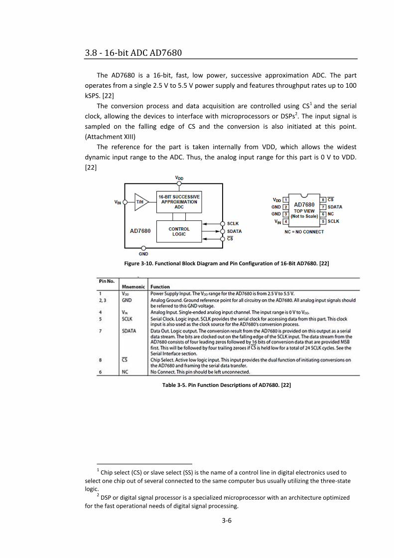
3.8 - 16-bit ADC AD7680
The AD7680 is a 16-bit, fast, low power, successive approximation ADC. The part
operates from a single 2.5 V to 5.5 V power supply and features throughput rates up to 100
kSPS. [22]
The conversion process and data acquisition are controlled using CS1 and the serial
clock, allowing the devices to interface with microprocessors or DSPs2. The input signal is
sampled on the falling edge of CS and the conversion is also initiated at this point.
(Attachment XIII)
The reference for the part is taken internally from VDD, which allows the widest
dynamic input range to the ADC. Thus, the analog input range for this part is 0 V to VDD.
[22]
Figure 3-10. Functional Block Diagram and Pin Configuration of 16-Bit AD7680. [22]
Table 3-5. Pin Function Descriptions of AD7680. [22]
1 Chip select (CS) or slave select (SS) is the name of a control line in digital electronics used to
select one chip out of several connected to the same computer bus usually utilizing the three-state logic.
2 DSP or digital signal processor is a specialized microprocessor with an architecture optimized
for the fast operational needs of digital signal processing.

4-1
Chapter 4. Hamamatsu Image Sensors
Datasheets Information
Note.: This chapter is an adaptation of information obtained in each equipment manual
(referenced in the bibliography) and introduces the equipment to the reader before
analyzing results.
4.1 - FFT-CCD C5809 Image sensor
The C5809 series multichannel detector head consists of a thermoelectrically-cooled
FFT-CCD image sensor, a low-noise driver/amplifier circuit and a temperature control
circuit. This combination enables stable operation of the image sensor by input of simple
external signals. [29]
The driver/amplifier circuit provides various timing signals necessary to operate the
image sensor and processes the analog video signal from the image sensor with a low
degree of noise. This circuit operates from two kinds of external control signals (Start, CLK)
and four different supply voltages (+5V, +15V, -15V, +24V). (See Chapter 3)
4.1.1 - Timing signal generator
Consisting of a counter and EPROM, the timing signal generator supplies various timing
signals. It also provides trigger signals (Trigger) for external A/D conversion (See
Attachment XIII). These signals are synchronized with external master clock pulse signals
(CLK) and initialized by start pulse signals (Start).
4.1.2 - Voltage regulators
The voltage regulator generates various voltages necessary to operate the image
sensor. Each voltage is generated by a low noise regulator with a high degree of accuracy
and stability. (See Chapter 3)
Note1.: For operating procedures see Attachment VII
Note2.: If “Green” LED is ON, indicates that the cooling temperature is set to the
present level (TS = 0 ºC).If “Red” LED is ON, warns that overheat is occurring due to
electrical open or short circuit of the thermistor in the image sensor, or failure of the
thermoelectric cooler. In this case we immediately turn the power off.

4-2
4.1.3 - Inputting the control signal from the PIC (Start and CLK)
Inputting two kinds of control signals (Start, CLK) from the PIC to the driver/amplifier
circuit. The pulse width of the “Start” signal must be longer than one cycle of the “CLK”
signal, and should be synchronized with the “CLK” signal as much as possible.
The “CLK” signal frequency determines the readout frequency of the “Data Video”
signal, and the pulse interval of the “Start” signal determines the storage time to the image
sensor.
Using the FFT-CCD image sensor operated at “CLK” signal frequency of 1MHz:
The readout frequency for the “Data Video” signal is 1/4th the “CLK” signal frequency
(See Attachment VII). The readout time per one channel, tv, is 4us.
The binning operation frequency is 1/16th the “CLK” signal frequency. The binning
operation time per one channel, tb, is 16us.
Thus, the time required for one scan, tscan, including the binning operation time
becomes
Equation 4-1. Time required for one scan of the FFT-CCD image sensor.
Where:
Nv – Number of channels of the vertical register.
Nh – Number of channels of the horizontal register.
Note.: See Attachment VIII
4.2 - S3921-128Q MOS Linear Image Sensor
The S3921 MOS linear image sensor feature a signal processing circuit which integrates
a signal charge in the inner video line and performs impedance conversion to provide an
output signal with a boxcar waveform. This allows signal readout with a simple external
circuit. The S3921 also have a wide photosensitive area with a pixel height of 2.5mm and a
pixel pitch of 50µm. [28]
4.2.1 - Driver Circuit
Driving the MOS shift register requires a start pulse (ɸst) and two.phase clock pulses
(ɸ1, ɸ2). The polarities of ɸst, ɸ1 and ɸ2 are positive. ɸ1 and ɸ2 can be either fully
separated or in the complementary relation. However, the overlap should not exist at the
rise or fall edge between ɸ1 and ɸ2. In other words, ɸ1 and ɸ2 must not be at the high

4-3
level at the same time. The pulsewidth of ɸ1 and ɸ2 must be longer than 200 ns. Since the
photodiode signal is obtained at the rise of every ɸ2, the clock pulse frequency determines
the video data rate. [28]
The amplitude of ɸst should be equal to that of ɸ1 and ɸ2. The shift register starts to
read out the signal with the high level of ɸst, so the time interval of each ɸst determines
he signal accumulation time. The pulsewidth of ɸst must also no longer than 200 ns and
must be overlapped with ɸ2 for at least 200 ns. Moreover, in order to start the shift
register normally, ɸ2 must be changed only once from the high level to the low level during
the high level of ɸst.
Note.: The timing diagram for each pulse is shown in Figure 4-1 and the respective time
values are shown in Attachment XI.
Figure 4-1. Timing diagram for drive circuit of S3921-128Q MOS Linear Image Sensor [28].
4.2.1 - Signal Readout Circuit
The amplitude of the reset pulse (Reset ɸ) should be equal to ɸ1, ɸ2 and ɸst. When
the Reset ɸ is at the high level, the video line is set at the reset voltage (Reset V). It is
recommended that the reset voltage be set at 2.5V when the amplitude of ɸ1, ɸ2, ɸst and
Reset ɸ is 5V. However, the sensor is to be powered by PIC that has signal whose peak is
4.9 volts. So, here we have a problem that is discussed in Chapter 8.

4-4
The fall of Reset ɸ must be prior to the rise of ɸ2 because the photodiode signal is
obtained at the rise of ɸ2. To obtain a stable output, an overlap between the reset pulse
(Reset ɸ) and ɸ2 must be settled, and furthermore, the fall edge of Reset ɸ should be
delayed from the fall edge of ɸ2.
The linear image sensor provides an output signal with negative polarity boxcar
waveform which includes a DC offset of approximately 1V when the reset voltage is 2.5V.
When it is desired that the DC offset is null and the waveform is inverted to the
positive polarity, a signal readout circuit and pulse timing is shown in Figure 4-2.
Figure 4-2. Recommend readout circuit and pulse timing for S3921-128Q MOS Linear Image Sensor.[28]
Note.: In this circuit, RS must be larger than 10 kΩ. Also, the gain is determined by the
ratio of Rf to RS, so, choose the value of Rf that suits our application.
The communication of all the sensor signals to the PIC is made through a connecting
header. The header is shown in Figure 4-3 and PCB is shown in Attachment XIV.
Figure 4-3. Header for communication between MOS and PIC.

5-1
Chapter 5. Temperature Monitor for a Liquid Xenon Detector
Having learned the ongoing project and the potential of our instrumentation, the
Laboratory of Instrumentation and Experimental Physics of Particles (LIP-Coimbra)
requested our collaboration for routinely screened a system that will serve to control the
temperature of a liquid xenon detector.
5.1 - LIP - Laboratory of Instrumentation and Experimental Physics of Particles
LIP is a technical and scientific association of public utility that aims to research in the
field of Experimental High Energy Physics and Associated Instrumentation.
Research fields of the LIP have grown to encompass the Experimental High Energy
Physics and Astroparticle, Radiation Detection Instrumentation, Data Acquisition and Data
Processing, Advanced Computing and applications in other fields, in particular the Medical
Physics.
The main research activities of the laboratory are developed within large collaborations
at CERN and other international organizations and major infrastructure inside and outside
Europe, such as ESA, SNOLAB, GSI, NASA and AUGER.
The LIP is an "associated laboratory" assessed as "Excellent" in three successive
evaluations by international panels.
In its three laboratories in Coimbra, Lisbon and Minho, LIP has about 170 employees, of
which more than 70 PhDs, and many teachers in local universities.
The center of Coimbra has a long experience in R&D of radiation detection systems and
their applications in experiments. Its activity is supported by a well equipped machine shop
and expert staff.[24]
5.2 - 1N4148 diodes
The 1N4148 is a standard silicon switching diode. Its name follows the JEDEC
nomenclature. The 1N4148 has a DO-351 glass package and is very useful at high
frequencies with a reverse recovery time of no more than 4 ns. It was second sourced by
many manufacturers; Texas Instruments listed their version of the device in an October
1966 data sheet. [25, 26]
1 The DO-35 is a semiconductor package type. It is often used to package small signal, low power
diodes (a 100V, 300mA silicon diode). Generally a diode will have a line painted near the cathode end.

5-2
5.2.1 – Specifications
VRRM = 100 V (Maximum Repetitive Reverse Voltage)
IO = 200 mA (Average Rectified Forward Current)
IF = 300 mA (DC Forward Current)
IFSM = 1.0 A (pulse width = 1 sec), 4.0 A (pulse width = 1 µsec) (non-repetitive peak
forward surge current)
PD = 500 mW (power Dissipation)
TRR < 4 ns (reverse recovery time)
5.3 - PCB
The PCB will be used to measure the temperature at two points (at the bottom and
along the photomultiplier) of a detector which will be used to estimate the reflectivity of
PTFE (commonly referred to as Teflon) to light the Xenon scintillation fluid, and with PTFE
immersed in liquid xenon. [30]
Figure 5-1. PCB used to measure the temperature of the D1 and D2 diodes.
Legend of Figure 5-1:
1 –"+12 V" and "-12" power supplies
2 – (J2) "+5 V" square wave
3 – (J3) signal to be measured by our ADC
D1 and D2 - 1N4148 standard silicon switching diodes
5-3
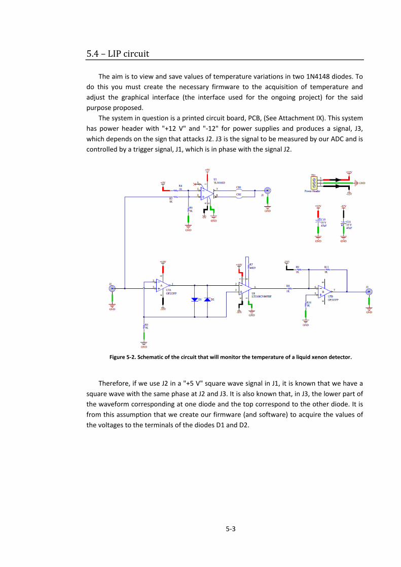
5.4 – LIP circuit
The aim is to view and save values of temperature variations in two 1N4148 diodes. To
do this you must create the necessary firmware to the acquisition of temperature and
adjust the graphical interface (the interface used for the ongoing project) for the said
purpose proposed.
The system in question is a printed circuit board, PCB, (See Attachment IX). This system
has power header with "+12 V" and "-12" for power supplies and produces a signal, J3,
which depends on the sign that attacks J2. J3 is the signal to be measured by our ADC and is
controlled by a trigger signal, J1, which is in phase with the signal J2.
Figure 5-2. Schematic of the circuit that will monitor the temperature of a liquid xenon detector.
Therefore, if we use J2 in a "+5 V" square wave signal in J1, it is known that we have a
square wave with the same phase at J2 and J3. It is also known that, in J3, the lower part of
the waveform corresponding at one diode and the top correspond to the other diode. It is
from this assumption that we create our firmware (and software) to acquire the values of
the voltages to the terminals of the diodes D1 and D2.

6-1
Chapter 6. Firmware At the end of this section we should have developed an understanding of the core
features of the MPLAB C32 C compiler, including its libraries and the core features of the
programming language C.
6.1 - Introducing MPLAB
MPLAB is an IDE1 hat can be downloaded free from Microchip’s web site. There is also a
copy on the book’s companion website and contains all the software tools necessary to
write a program in Assembler, assemble it, simulate it, and then download it to a
programmer. Further software tools can be bought and then integrated with MPLAB, both
from Microchip and from other suppliers. This includes alternatives to what MPLAB already
offers – e.g. assemblers or simulators, as well as tool which offer much greater
development power, like C compilers or emulator drivers. [15]
6.2 - The elements of MPLAB
MPLAB is made up of a number of distinct elements which work together to give the
overall development environment. These are:
Project Manager – The preferred way of developing programs in MPLAB is by
creating a project. An MPLAB project groups all the files together that relate to
the project and ensures that they interact with each other in an appropriate
way and are updated as needed.
Text Editor – This allows entry of the source code. It behaves to some extent
like a simple text editor such as Notepad, but it can recognize the main
elements of the programming language that is being used.
Assembler and Linker – The function of the Assembler we have assumed that
there is a single source file. The role of the Linker is to put the code, may be
created from a number of different files, together; give each its correct location
in memory and ensure that blanches and calls from one file to the other are
correctly established.
Software Simulator and Debugger – A software simulator allows a program to
be tested by running it on a simulated CPU in the host computer. The debugger
contains the tools which allow program execution to be fully examined.
1 Integrated Development Environment (IDE) is a software application that provides
comprehensive facilities to computer programmers for software development. An IDE, normally, consists of a source code editor, build automation tools and a debugger.

6-2
6.3 - MPLAB C32 C Compiler
6.3.1 - File Naming Conventions
The compilation driver recognizes the following file extensions, which are case
sensitive.
Extensions Definition
file.c A C source file that must be preprocessed
file.h A header file (not to be compiled or linked)
file.i A C source file that has already been pre-processed
file.o An object file
file.s An assembly language source file
file.S An assembly language source file that must be preprocessed
other A file to be passed to the linker Table 6-1. File extensions names in compilation driver.
6.3.1.1 - Data Storage
Storage Endianness
MPLAB C32 C compiler stores multi-byte values in little-endian format. That is, the least
significant byte is stored at the lowest address.
For example, the 32-bit value 0x12345678 would be stored at address 0x100 as:
Table 6-2. Example of stored at address 0x100 of 32-bit value 0x12345678.
Integer Representation
Integer values in MPLAB C32 C compiler are represented in 2's complement and vary in
size from 8 to 64 bits. These values are available in compiled code via limits.h. The limits.h
header file defines the ranges of values which can be represented by the integer types.

6-3
Table 6-3. Integer representation values in MPLAB C32 C Compiler.
Signed and Unsigned Character Types
By default, values of type plain char are signed values. This behavior is implementation-
defined by the C standard, and some environments define a plain char value to be
unsigned. The command line option -funsigned-char can be used to set the default type to
unsigned for a given translation unit.
Floating-Point Representation
MPLAB C32 C Compiler uses the IEEE-7541 floating-point format. Detail regarding the
implementation limits is available to a translation unit in float.h.
Table 6-4. MPLAB C32 C Compiler floating-point format.
6.3.2 - Pragmas (pragmatic information)
The “#pragma” directive is the method specified by the C standard for providing
additional information to the compiler, beyond what is conveyed in the language itself..
#pragma interrupt
Mark a function as an interrupt handler. The prologue and epilogue code for the
function will perform more extensive context preservation.
#pragma vector
Generate a branch instruction at the indicated exception vector which targets the
function.
1 IEEE Standard for Floating-Point Arithmetic (IEEE 754) is a technical standard for floating-point
computation established in 1985 by the Institute of Electrical and Electronics Engineers (IEEE).

6-4
#pragma config
The #pragma config directive specifies the processor-specific configuration settings
(i.e., configuration bits) to be used by the application.
6.3.3 - Interrupts
Interrupt processing is an important aspect of most microcontroller applications.
Interrupts may be used to synchronize software operations with events that occur in real
time. When interrupts occur, the normal flow of software execution is suspended and
special functions are invoked to process the event. At the completion of interrupt
processing, previous context information is restored and normal execution resumes.
PIC32MX devices support multiple interrupts, from both internal and external sources.
The devices allow high-priority interrupts to override any lower priority interrupts that may
be in progress.
The MPLAB C32 C Compiler provides full support for interrupt processing in C or inline
assembly code.

7-1
Chapter 7. Software
7.1 - Visual C++/CLI
The .NET platform appears to be the future, especially now that is largely standardized.
Therefore, it is not surprising the huge amount of companies and developers interested in
.NET programming, using in particular the Visual Studio development environment. We also
know that there are many who program in C and C++ (the language most used in the
production of games).
The Visual C++ allows to program according to the open standard C++/CLI (Common
Language Infrastructure) ECMA1. When programming in accordance with this standard, the
programmer produces code for the standard .NET, which facilitates its portability and
interoperability between languages. On the other hand, the Visual Studio enables those
who want, ignoring the many peculiarities and proprietary technologies that were
inescapable in previous .NET versions. To build the graphical interface is used the 2008
version of Visual Studio C++, following the new standard C++/CLI, and all code is compatible
with the framework 3.5. [32]
7.1.1 - .NET
The .NET is a platform oriented for Internet and its main function is to provide software
as a service. The three main components are shown in the next figure. At the highest level
are the development tools, for example, Visual Studio .NET.
Figure 7-1. Framework .NET architecture diagram.
1 ECMA (European Computer Manufacturers Association) is an association founded in 1961
dedicated to the standardization of information systems. Since 1994, became the Ecma International to reflect its international activities. Membership is open to companies that manufacture, sell or develop computer systems or communication in Europe.

7-2
7.1.2 - Framework .NET
It is an infrastructure development and execution with its own class library (Base Class
Library - BCL) and its runtime (CLR).
The main objectives of the Framework .NET are:
Infrastructure components - allowing a simple way to integrate libraries
complicated without changing the source code.
Integration of language - a language class can inherit from other languages,
e.g. .NET all objects derived from a root class System::Object.
7.1.3 - Common Language Runtime
The CLR is the most important component Framework .NET, which provides a secure
execution environment and a high performance applications. In addition, it’s designed to
be driven code execution for all languages and possibly multiple platforms.
The Visual C++ is the only language you can mix managed1 code with non-managed
(native2). In .NET data types can be described as reference types (example: ARRAY, HANDLE
…) or value types 3 . Reference types are considered managed. The CLR allows
interoperation between managed and native code. The terms managed and native refer to
how memory space is reserved for the types of instances and how it is carried out
management of the memory.
An instance of a managed type created with gcnew operator is always placed on the CLI
heap.
In C++/CLI, a variable of a native type can be created on the stack, but it is created on
the heap will be used to release native C++ operator new and types will be created on the
heap of the native C++. For these types will require the programmer to free the memory of
these objects using the delete operator of the native C++. In the case of managed types,
this is not necessary for this task rests with the CLR.[32]
1 Managed code is code that has its execution managed by the .NET Framework Common
Language Runtime. It refers to a contract of cooperation between natively executing code and the runtime. This contract specifies that at any point of execution, the runtime may stop an executing CPU and retrieve information specific to the current CPU instruction address. Information that must be query-able generally pertains to runtime state, such as register or stack memory contents.
2 Native code it's a code that is compiled to run with a particular processor and its set of
instructions. If the same program is run on a computer with a different processor, software can be provided so that the computer emulates the original processor.
3 Value types represent values allocated in the program stack and are the legacy (directly or
indirectly) from the System::ValueType class.

7-3
7.2 - Windows Forms
Using the tools in the toolbox Visual Studio C++ was possible to construct a graphical
user interface that enables interactive graphical quite handling various external devices
that can be connected to the microcontroller.
Figure 7-2. Image of the first Form of the graphical user interface (GUI).
The tool Windows Forms of the Microsoft Visual Studio C++ allows creating new Forms,
i.e., we are not restricted only one window may be (as is the case) multiple windows in
parallel which enables a more didactic with user.
In the Figure 7-2 you can see several buttons. Some of these buttons open new
windows (Forms) where we can selected parameters and devices that we want to control.
In the following chapter (Chapter 8. Results) will be given more information about
Windows Forms.

8-1
Chapter 8. Results
8.1 - The graphical interface (GUI)
There were some problems when upgrading the graphical interface that already
existed. We chose to build a new graphical user interface, more robust and more didactic.
Due to the complexity of construction, I'll just present how is the communication between
various Forms.
8.1.1- Communication between Forms
When starting a new project (Windows Forms Application) is generated a Form with
Form1.h original name. This Form is a header file without a .cpp source file. Thus, all code is
inserted into the header. From here, any new Form created has to be included in an include
header file created at beginning of project, the name of this file is stdafx.h.
For communication between Forms we use functions of windows language.
Figure 8-1. Communication between two Windows Forms
Figure 8-1 shows the communication between two Forms (Form1 and ADCForm).
Example 8-1 shows the code entered on Form1 to have dialogue with ADCForm.
Example 8-1. Code for communication between two Windows Forms
ADCForm ^adc = gcnew ADCForm();
adc->ShowDialog();
textBox1->Text = "ADC";
textBox2->Text = Convert::ToString(Parametro.tempo_amostragem);
textBox3->Text = Convert::ToString(Parametro.numero_amostras);
textBox4->Text = "n. a.";

8-2
8.2 - Data Visualization
An important part of this project was the visualization of the data received in
continuous mode. This was achieved by manipulating the object Chart of the toolbox of
Microsoft Visual Studio C++.
Chart object can paint values in an ArrayList. To re-paint a new set of values has
created an array and then inserted into an ArrayList. Before re-paint new data, is made a
Clear and it’s incorporate a new array values in ArrayList by an Add. Whenever the Chart
paints a data set and we use the Update function to force Chart to change their status.
Below is shown a partial code used to display data in continuous mode.
Example 8-2. Partial code to display data in continuous mode.
The Update function is used to update other objects of the Microsoft Visual Studio C++
toolbox. It is the case of labels used to count the number of acquisitions.
Note.: The Example 8-2 is not the full code for the visualization of data in continuous
mode, is just one example that demonstrates the use of some functions of Windows
language. In this example, the data received by USB communication are shown in Chart1.
8.2.1 - Save data in .txt format.
All acquisitions can be saved in .txt format. The partial code of Example 8-3 shows how
this storage is done
ArrayList ^ xvals = gcnew ArrayList();
ArrayList ^ yvals = gcnew ArrayList();
int scan[scan_length];
int s_index = 0;
scan[s_index++] = Data_int;
for(int i = 0; i< scan_length ; i++)
{
yvals->Add(scan[i]);
xvals->Add(i);
}
chart1->Series["Series1"]->Points->DataBindXY(xvals,yvals);
chart1->Update();

8-3
Example 8-3. Partial code for storage in .txt format.
Note.: They can also be stored images that are to be printed on the screen. To do so,
use the following line of code:
chart1->Serializer->Save("C:\\Users\\Asus\\Desktop\\UI\\Neurocornea\\SAVES\\ChartImage\\CCD\\" +
textBox5->Text + " scan n. " + (NumeroAquisicoesPIC+1));
8.3 - Communication between PC and PIC
Another very important part of this project is to develop the communication between
user and PIC by USB communication. Improve how data is sent and received is the first step
to get a better sampling in Chart of the GUI.
The development of a USB communication is highly complex. To program this PIC
microcontroller it’s used a library provided by Microchip called LibUSB. This is an open
source library that allows access to USB devices once recognized VID/PID of the device.
The library used has a USB output and a bulk endpoint and transfers is set to Full-
Speed. Thus, each bulk transfer has up to 64 bytes per data packet.
The USB communication had been established the previous year. However, was
created a variable able to send values to the PIC
8.3.1 - Sending Data to PIC Firmware
To be able to visualize the data in continuous mode is required, firstly, more than one
data packet (scans) to be sampled.
The Example 8-4 shows how values of parameters are sent to the PIC.
using namespace System::IO;
… FileStream ^ outFile = gcnew
FileStream("C:\\Users\\Asus\\Desktop\\UI\\Neurocornea\\SAVES\\Files
ASCII\\Temperatura\\" + textBox5->Text + ".txt", FileMode::Append,
FileAccess::Write);
StreamWriter ^streamOut = gcnew StreamWriter(outFile);
… streamOut->WriteLine(Data);
… streamOut->WriteLine("END OF ACQUISITION");
streamOut->Close();

8-4
Example 8-4. Partial code that shows how values of parameters are sent to the PIC.
Obviously, firmware reads all of these values. The Example 8-5 shows partial code of
this interpretation and application of the one value.
Example 8-5. Partial code of MPLAB Firmware.
8.3.2 - Sending Data to PC Software
As stated, the USB communication established does not support more than 64 bytes
(64 chars) per download package. Thus, 512 (or 128) conversions have to be separated by
data packets to be sent to get the PC.
The result of a conversion occupies 2 bytes. In automatic mode, packets are sent with
32 conversions. Thus, for conversions with 512 points, this will be sent 16 packets. [27]
In Example 8-6 is shown a partial code used to send conversions.
char OutputPacketBuffer[64];//Allocate a memory buffer which will
contain data to send to the USB device
OutputPacketBuffer[0] = 0x82; //0x82 command in the firmware
OutputPacketBuffer[1] = Parametro.tempo_amostragem;
OutputPacketBuffer[2] = Parametro.numero_amostras;
OutputPacketBuffer[3] = Parametro.pix_duration;
//Writes data to a bulk endpoint. The Function call will send out 64
bytes to the USB Device.
if(usb_bulk_write(MyLibusbDeviceHandle, 0x01, &OutputPacketBuffer[0],
64, 5000) != 64)
return;
}
case 0x82:
pix_end = OUTPacket[1];
scans_end = OUTPacket[2];
naq_end = OUTPacket[3];
…
T3CON = 0; //Disable Timer 3. Write bits configurations
TMR3 = 0;
PR3 = pix_end; …

8-5
Example 8-6. Partial code used to send 512 conversions to PC.
9.3.2.1 - How conversions are made
Before data is sent to PC, PIC has to do conversions. In all cases (ADC at maximum rate,
FFT-CCD, MOS, LIP circuit), is used OC3 (Output Compare 3), an OC module of the PIC.
Below is the code used to make ADC conversions.
Example 8-7. Partial code used to make ADC conversions
//Data transfer throw usb
unsigned int b;
for(b=0;b<16;b++)
{
unsigned short int t;
for(t=0;t<32;t++)
{
DataToTransfer[t]=DataToTransfer[t+(b*32)];
}
unsigned int j,i;
for(j=0, i=0;j<64;j++)
{
INPacket[j]=DataToTransfer[i];
j++;
INPacket[j]=DataToTransfer[i]>>8;
i++;
}
if(!USBHandleBusy(USBGenericInHandle))
{
USBGenericInHandle =
USBGenWrite(USBGEN_EP_NUM,(BYTE*)&INPacket,USBGEN_EP_SIZE);
}
DelayMs(1);
}
void __ISR( _OUTPUT_COMPARE_3_VECTOR, ipl3) OC3Handler(void)
{
static unsigned int spidata;
SPI1BUF = 0x00000000;
while( !SPI1STATbits.SPIRBF);
spidata=SPI1BUF;
unsigned short int spidata2 = spidata >> 13;
DataToTransfer[mais2]=spidata2;
mais2++;
IFS0 &= 0xFFFFBFFF;
} …
SetTimer2();
//OC3 interrupt enable (in the interrupt the acquisition will be made)
IFS0 &= 0xFFFFBFFF; //Clear OC3 Flag
IEC0 |= 0x00004000; //Set OC3 Interrupt
IPC3 |= 0x000C0000; //Priority = 3
OpenOC3(OC_ON | OC_TIMER2_SRC | OC_CONTINUE_PULSE , 100 ,0 );
while(mais2<512); //Counter of 512 acquisitions
//Reset OC3 and Timer2
CloseOC3();
Timer2Reset();

8-6
8.4 - ADC Tests
From the GUI, user can visualize any signal that is connected to the ADC input. This case
does not take into account any particular temporization and ADC will convert at the
maximum rate (100 kSPS). In this case there may be some problem in visualization, since
there is no time been able to transfer a data packet before another package begins to be
send. Therefore, a brief interruption is used (which may be increased in GUI) to enable the
correct transmission of data before starting next acquisition.
Figure 8-2. ADC WindowsForm image where the ADC parameters are selected.
Note.: In the case of ADC, the exposure time and has no units because there is no need,
the intention is just a “groove” in any acquisition.
8.4.1 - Effective number of bits (ENOB) of the 16-bit ADC AD7680
All signals contain a certain amount of noise. If the drive is able to represent the signal
levels below the noise floor of the system, the lower bits of the digitized signal representing
only system noise and contain no useful information. ENOB specifies the number of bits in
the digitized signal above the background noise.
Equation 8-1. An often used definition for ENOB.
Where all values are given in dB, and:
SINAD is the ratio of the total signal including distortion and noise to the
wanted signal
The 6.02 term in the divisor converts decibels (a log10 representation) to bits (a
log2 representation)
The 1.76 term comes from quantization error in an ideal ADC

8-7
Equation 8-2. An often used definition for SINAD.
Where SNR is a Signal-to-Noise ratio. From ADC AD7680 datasheet, we know that in our conditions SINAD = 87.82 dB.
Note.: We can see that this value corresponds to reality if we look Figure 8-3.
8.1.1.1 - 1.3 Volts battery test
In order to test the certainty of ADC conversion, a test was done with a 1.3 volt battery.
2560 points were acquired (5 acquisitions of 512 points) and obtained the results shown in
the Table 8-1:
Average 17755.27
Standard Deviation 14.03055
Maximum 17820
minimum 17632
Table 8-1. Analysis of points converted by the ADC subjected to a potential of 1.3 volts.
However, if we do the same calculations but now for an acquisition of 512 points (each
acquisition will have a maximum of 512 points):
Average 17746.99
Standard Deviation 8.061647
Maximum 17802
minimum 17632
Table 8-2. Analysis of one acquisition with 512 points, converted by the ADC subjected to a potential of
1.3 volts.
From standard deviation, we have a better performance of the ADC in a single
acquisition.
This difference has to do with the values that the ADC converts each acquisition. It was
found that one acquisition to another exists or a rise or fall of converted values, as shown
in Figure 8-3.
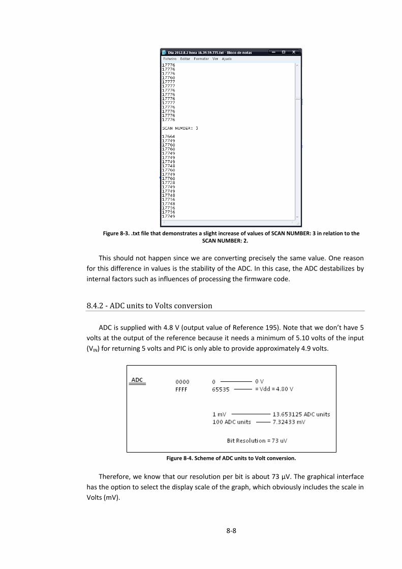
8-8
Figure 8-3. .txt file that demonstrates a slight increase of values of SCAN NUMBER: 3 in relation to the
SCAN NUMBER: 2.
This should not happen since we are converting precisely the same value. One reason
for this difference in values is the stability of the ADC. In this case, the ADC destabilizes by
internal factors such as influences of processing the firmware code.
8.4.2 - ADC units to Volts conversion
ADC is supplied with 4.8 V (output value of Reference 195). Note that we don’t have 5
volts at the output of the reference because it needs a minimum of 5.10 volts of the input
(VIN) for returning 5 volts and PIC is only able to provide approximately 4.9 volts.
Figure 8-4. Scheme of ADC units to Volt conversion.
Therefore, we know that our resolution per bit is about 73 µV. The graphical interface
has the option to select the display scale of the graph, which obviously includes the scale in
Volts (mV).

8-9
8.4.3 - SPI communication
Communication between PIC and ADC is done via SPI communication [Attachment XIII].
Since this is a continuing project, this communication was already established. However,
everything that concerns the code used in firmware has not been substantially changed.
Moreover, electrical connections of the PIC pins to ADC pins have been changed, since the
ADC was placed on daughter board.
Figure 8-5. Microchip PICtail Plus Daughter Board with components.
Legend of Figure 8-5:
1 -16-bit ADC AD7680
2 - ADC Reference 195
3 - Start, Clock and Trigger
4 -ADC Input
5 -signals for MOS
6 - GND
The Figure 8-6 shows a schematic of the correspondence of the pins of the ADC and the
pins of the PIC.
Figure 8-6. Schematic of the correspondence between ADC pins and PIC pins.

8-10
Note.: For more information about the communication between PIC and ADC see
Attachment XIII and Chapter 3.
8.5 - FFT-CCD image sensor
Results presented to the FFT-CCD image sensor are based only on simulations since this
device had a breakdown during the course of project. To continue the work we opted for a
sensor that was in stock, S3921-128Q MOS Linear Image Sensor, whose results were quite
satisfactory and will be presented later in this thesis.
8.5.1 - External control signals
The FFT-CCD image sensor circuit operates from two kinds of external control signals
(Start and Clock). The master clock pulse and start pulse signals are generated by PIC. Upon
receiving these signals, FFT-CCD image sensor is able to send a signal (Trigger) for external
A/D conversions, in this case, informs our firmware when you can do conversions.
Figure 8-7. Header (in PIC daughter board) for connecting the Start and Clock signals FFT-CCD image
sensor and for connection of Trigger signal to the PIC.
This circuit operates from four different supply voltages (+5V, +15V, -15V, +24V). These
supply voltages are provided by regulators that were described in Chapter 3. All signals and
power supplies are connected to the FFT-CCD image sensor by a 15-pin D-SUB Connector
can see that in view Attachment VI.
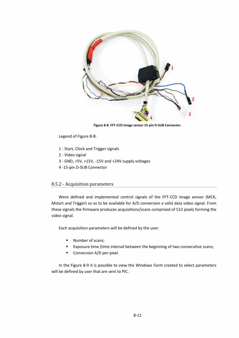
8-11
Figure 8-8. FFT-CCD image sensor 15-pin D-SUB Connector.
Legend of Figure 8-8:
1 - Start, Clock and Trigger signals
2 - Video signal
3 - GND, +5V, +15V, -15V and +24V supply voltages
4 -15-pin D-SUB Connector
8.5.2 - Acquisition parameters
Were defined and implemented control signals of the FFT-CCD image sensor (MCK,
Mstart and Trigger) so as to be available for A/D conversion a valid data video signal. From
these signals the firmware produces acquisitions/scans comprised of 512 pixels forming the
video signal.
Each acquisition parameters will be defined by the user:
Number of scans;
Exposure time (time interval between the beginning of two consecutive scans;
Conversion A/D per pixel.
In the Figure 8-9 it is possible to view the Windows Form created to select parameters
will be defined by user that are sent to PIC.

8-12
Figure 8-9. Picture of the selection window of FFT-CCD parameters.
Note 1.: In this case we have an exposure time limit (4s). The time defined by user is is
the time of each acquisition (512 points with a line of 3216 clocks). Thus, after an
acquisition the values are sent to PC and software processes these values. If exposure time
is more than 4 seconds, software does not respond because time of USB communication.it
exceeded.
Note 2.: This exposure time was not calculated, it was verified experimentally. Also
mean that the exposure times and conversions per pixel are not easy to calculate because
it does not depend only for interruptions but also data transmission and processing time
code. On the other hand, it is defined that the maximum time that a USB communication is
available is five seconds.
8.5.3 - Disk storage
The software is able to automatically store acquisitions in ASCII format. The file names
are automatically set and contains the time of recording (so we avoid writing the name of
the file, which would waste time between two consecutive acquisitions). Are also stored
individual scans, parameters of acquisition and other descriptive information.
The graphical interface created is able to save the acquisitions in “.file” format. So,
these images can be viewed later using the same platform.

8-13
8.5.4 - Processing of Data
It is possible the processing of files like: determination of mean and standard deviation,
peak values; loading several acquisitions (aquis1, aquis2, etc.) for comparison and
determination of differences.
8.6 - LIP – Temperature Monitor for Liquid Xenon Detector
The aim is to view and save values of temperature variations in two 1N4148 diodes.
To meet the challenge, our code of firmware is able to receive a square wave signal
(trigger) and convert various points in higher and lower level of the square wave.
From graphical interface user can select number of acquisitions (number of
measurements for each temperature of the diode). In each acquisition are made 256
conversions of the D1 and 256 conversions of D2 temperatures (total of 512 points), and
from this the software make an average for each 256 conversions. Was chosen this method
because we have enough time to do so, each data array sent to software had a length of
512 values and more than one point minimizes substantially the noise error.
Figure 8-10. Scheme illustrating the 1 Hz square wave used as a trigger to synchronize conversions of
diode D1 and diode D2.
The wave serving as a trigger which is 1Hz, ie, each cycle has a second. Therefore, we
make the first conversion when trigger = 1 (high level) and use an interruption with 0.25
seconds, when trigger = 0 (low level) we use the same interruption for the second
acquisition.
The graphical user interface created calculates mean and standard deviation for each
conversion and saves the corresponding values in .txt file format. Are also stored some
additional information such as time (in milliseconds) of the first conversion and it is known
that second conversion is 0.5 seconds later, third is 0.5 seconds later, until last conversion.

8-14
Figure 8-11. File in ASCII format which are stored the mean values and standard deviation of each D1 and
D2 conversion.
At the end are displayed in a graph all points relating each conversion. This image can
also be saved. During the various conversions are shown in the graph the points that are
being converted as well as mean, standard deviation, maximum and minimum values of
each conversion. Thus, it is possible to monitor the temperature variations in real time.
Figure 8-12. Picture of the GUI where we can view D1 and D2 variations.
Note.: In Figure 8-12, the range of values to the change in temperature of the diodes is
not very salient because we visualize the variation curves of the two diodes in the same
graph (chart). Using the values recorded on “.txt” file in excel page would have a results
from the Figure 8-13, where more easily visualize this variation.

8-15
Figure 8-13. Graphs of temperature variation in diodes D1 and D2. These graphs were obtained using an
excel sheet.
Note.: There was no need interest by us to record the temperature variations of the
diodes. The temperature varies between 24 º C and 70 º C (approximately). We had not a
particular interest in diodes calibration because it was not proposed to us at time. We take
the time to work on the most important aspects that we considered, how to make sure we
were doing the right conversions, calculate means and standard deviations.
8.7 - MOS Linear Image Sensor
This sensor was used due to damage that occurred with the Hamamatsu FFT-CCD
C5809 Image Sensor.
8.7.1 - External control signals
The MOS sensor circuit operates from some kinds of external control signals. All these
signals come from the PIC daughter board signals and are sent to the MOS sensor in a
header that is shown in Figure 8-14.
Figure 8-14. Header (in PIC daughter board) with all signals for MOS sensor.

8-16
8.7.2 - A/D Conversion
Since there was used the circuit shown in Figure 4-1, as stated in Chapter 4, the linear
image sensor provides an output signal with negative polarity boxcar waveform. Taking this
into account, the video signal that must be converted is the descending part of the output
signal. Thus, there is a portion which should remain constant that includes a DC offset of
approximately 1V when the reset voltage is 2.5V.and the other will vary with the light
enters on photodiode.
It was thought to make an acquisition of base (that part does not change) and signal
(part that varies with the light) and then do the subtraction. However, for a better
visualization of data we decided acquiring a part which varies with the amount of light that
falls on the detector and make processing in software, descending (negative) part.
8.7.3 - Pixel duration time
Another issue that should be talked about has to do with the duration of each pixel.
Firstly, it is noted that this is the most important parameter and is controlled by user. It is
the duration of each pixel that defines the exposure time for an acquisition.
To program duration of each signal in "MOS shift register" times that were used are
indicated in Figure 4-1 and Attachment X. However, to make sure we were on the parts you
want to convert the output signal, use an oscilloscope to check whether there was any
delay imposed by the operating system that would influence conversions.
Figure 8-15. Video output of S3921-128Q MOS linear image sensor in the oscilloscope and conversions to
be made.
Note.: In Figure 8-15 we can see the various conversions per pixel (20 conversions) that
are carried out on each "level" of the output signal. The output signal is a square wave
signal and the high level is the level of offset.

8-17
Figure 8-16. An acquisition of MOS.
In Figure 8-16 you can see the variation of the amount of light that is entering in
detector. More than that, it is possible to know the amount of light that is inserted in each
pixel. That is, each point on the graph corresponds to the respective pixel on the sensor.
Point 1 – Pixel 128; Point 128 – Pixel 1.
The exposure time that user selects is the exposure time for each pixel. Thus, this time
is the time between two consecutive phi_start (ɸst).
8.8 - Final prototype
The Figure 8-17 shows the final instrumentation prototype created. You can see the
power board, I/O Expansion Board with USB Starter Kit II and the connection to MOS. The
15-pin D-SUB Connector serves for connection to the FFT-CCD.
Figure 8-17. Final prototype with MOS.

8-18
Legend of Figure 8-17:
1 - PIC32 USB Starter Kit II
2 - I/O Expansion Board
3 - Microchip PICtail Plus Daughter Board.
4 - Power Supply Voltage Board
5 - FFT-CCD image sensor 15-pin D-SUB Connector
6 - S3921-128Q MOS Linear Image Sensor
In the Figure 8-17 it is possible to see a blue box where are placed the Power Board, the
I/O Expansion Board with USB Starter Kit II and PICtail Plus daughter board. This box has a
lid that when placed would complete the final prototype. The lid has the outputs cables for
USB PIC and other connecting cables. As a final model can’t end, the lid is not shown on the
picture. This lid would also reduce noise signal since exposure to external agents would be
substantially lower.
8.9 - Unsolved problems
As stated, the FFT-CCD had a malfunction during the project however, mean that the
instrumentation is prepared to receive the FFT-CCD. The FFT-CCD fault can be solved or
obtained a new and immediately placed in the instrumentation.
The J2 slot of the I/O Expansion Board is faulty. However this board has two slots for
PICtails and J4 is stable.
When sending data to the PC, sometimes the first data packet (32 points) arrives with
some errors. This happens when we have very small exposure times (milliseconds). This has
to do with shipping time USB communication, no time to send the packets correctly. To
improve this point we have to improve USB communication.
The maximum time for sending each data packet is 5 seconds, after which the USB
communication is broken, so each acquisition can’t last more than 5 seconds.
At the end, the S3921 MOS linear image sensor no longer has the desired sensitivity. By
this I mean that the image of the Figure 8-16 is no longer able to obtain due to a
malfunction. To rectify the fault are the following proposals:
Making an experience with another sensor
Placing the sensor on another signal board
Create a button on the GUI only for the sensor
It was found that the minimum voltage of each signal (Φ) must be 4.5 volts (low level).
However, the PIC logic outputs only provide 3.3 volts (even with 12 volts external supply).
Therefore, check if the problem keeps with 4.5 volts is also a proposal to try to fix the
problem of sensor sensitivity.

8-19
To be able to place all signals with 4.5 V can be used a state buffer/line driver (HCT244).
The Figure 8-18 shows the schematic which would be used for this purpose.
Figure 8-18. Schematic with state buffer/line driver (ex.: HCT244).
For the GUI created, this serves the purpose perfectly for sampling data. However,
there was one thing that was not quite finished. When sampling data packets, it is not
possible to stop viewing without using commands in Microsoft Visual Studio C++. By this I
mean that as there is a button that initiates acquisitions, it would be great to program a
button to stop the acquisition. This goal is not easy conclusion once during the course of an
event (eg, reading the code of a button) do not have access to another event until the first
finish.
All connections between the components of the power board and PICtail have been
checked and are stable. However, to improve the quality of the signals a PCB would be the
ideal solution. It would also be very important to put all entries of the devices in the
housing lid and close the box in order to give greater security to the PIC and power board.
During the project, some of our PIC had a malfunction described in Example 8-8. The
Microchip Technical Support was contacted and the solution was the replacement of new
PIC.
Example 8-8.Example of PIC problem description.
Target Device ID (000FF000) does not match expected Device ID (00007000). Device reset failed Make sure Configuration Bits are correct. PIC32 Starter Kit hardware initialization failure. Error = -1, Detail = 0x00000000 (LID: 29) Device reset failed Make sure Configuration Bits are correct.

9-1
Chapter 9. Conclusion and Future work
During the course of the project always occurring several problems that have been
solved. However, the connection to the FFT-CCD image sensor was not possible because
this sensor was damaged during the project. But, from simulations, the entire firmware and
software is ready to accept this sensor.
The great advantage of FFT-CCD image sensor is undoubtedly the sensitivity but also
the cooling. That is, both the light intensity being received by pixel to charge and discharge
the capacitor at each pixel influence the signal that is read. Once cooled know that there is
no influence of warming in the video signal. So, switching to a MOS Linear Image Sensor
was not an advantage, but it was the only way to continue to get results.
The results presented in Chapter 8 have been met with success, is to say that most of
these results were not foreseen at the beginning of the project. One such example is the
application for the LIP circuit, which was performed with success. In this application has
been used quite ingenuity to adapt both the GUI as the firmware once created for this new
application.
At the end of all this work it is possible to convert any signal in continuous mode.
Overcoming this goal was not a simple question because it implies knowing very well the
capabilities of the toolbox of Microsoft Visual Studio C++, in this case, I had to study very
well the features of "Chart" object and the way to go "updating" the values that is
receiving. This is not so easy because we will have to make sure that we keep getting values
in an array that also has features very own, an "ArrayList". After overcome this aim, the
step for the display of any entry of a pin of the PIC was very simple.
The programming of MOS Linear Image Sensor was not very difficult because we only
had to generate (in PIC) the signals that it needs. In this case, there were not used OC’s
(output compares) as in the case of FFT-CCD image sensor. How times had with a very
precise synchronization between each signal, the work was done in order to go modifying
the state of each pin of the PIC to take the desired signals. As the video signal generated by
MOS sensor signal is not "real", this processing was done in software and the results are
visualized are very well understood.
A future work will adapt our firmware and software for different types of MOS Linear
image sensors (256, 512 and 1028 pixels). This work began to be done at the end of the
project but no time to finish. More future work will be able to send commands to the PIC.
Controlling interrupts, set timer values or choose if you want a 16 or 32 bit timer...
At LIP circuit work, was never made a rigorous calibration of diodes temperature
curves. The truth is that we have never been asked but would be a work that would make
viewing the varying temperatures of the diodes more easily understandable.
The graphical interface created can store all values acquired in ASCII format but also in
system image format. This image format is a system format and been able to be opened by
the GUI. Thus, future work would be able to do calculations from these images.
A point to be noted is that our system is prepared to convert any signal by a trigger.
That is, we have a digital input (pin AN2) of the PIC always active to use as a trigger.

9-2
However, all code would have to be changed according to the characteristics of the signal
that we want to convert.
As stated, the damage that had happened in the PIC as a PIC replacement solution (by
Microchip Technical Support), since the fault was in a kind the code protect ON (a kind of
fuse is burned), the starter kit is broken and the arrangement was difficult. These faults
could have occurred by several factors but surely these factors have resulted in a short
circuit that burned the fuse. I want to mean that rapid support from Microchip was crucial
to proceed with work on the project.
Finally, I say that the work was made with the knowledge acquired during the course of
project. Departure for this project I had no knowledge in C language, so the process of
programming the PIC involved a lot of learning both the equipment with its programming.
The process of building the GUI also involved to study windows language very closely and
successfully to control an object minimally.
Therefore, I am pleased with the work accomplished and, more than that, on
knowledge that I now have about managed devices. It should be noted that this project
involved manipulation of electronic devices and is placed on integrated circuits, and the
whole panoply of processes that have to be made for their recognition by PIC and uptake of
results for a graphical interface.

I
Bibliography
1. Vinik, A. I. et al. Diabetic Neuropthies. Diabetologia. 2000, Vol. 43, pp. 957-
973.
2. The Diabetes Control and Complications Trial Research Group. The Effect of
Intensive Treatment of Diabetes on the Development and Progression of Long-
Term Complications in Insulin-Dependent Diabetes Mellitus. The New England
Journal of Medicine. 1993, Vol. 329, pp. 977-986.
3. Boulton, Abdrew J. M. Management of Diabetic Peripheral Neuropathy.
Clinical Diabetes. Number 1, 2005, Vol. 23.
4. Lin, Helen C. and Quan, Dianna. Diabetic Neuropathy. Medscape Reference.
November 2011.
5. Morgado, António M. et al. Evaluation of Corneal Nerves Morphology for
Diabetic Peripheral Neuropathy Assessment. 2012.
6. NeuroCornea. NeuroCornea. [Online] 2011. [Cited: June 3, 2012.]
http://neurocornea.net78.net/home.html.
7. CPU World. CPU World. [Online] Gennadiy Shvets, 2003-2010. [Cited: June 4,
2012.] http://www.cpu-world.com.
8. Riley, H. Norton. The von Neumann Architecture of Computer Systems.
Pomona, California : s.n., September 1987.
9. Gonçalves, Victor. Sistemas Baseados em Microcontroladores PIC. Porto :
Publindústria, Edições Técnicas, 2008.
10. Hof., Philipp. Von Newmann’s Architecture. Electrical and Computer
Engineering. [Online] University of Canterbury - Christchurch, New Zealand.
[Cited: June 20, 2012.]
http://www.elec.canterbury.ac.nz/PublicArea/Staff/hof/p10-embed/p10-
tutorial/p12.html.
11. ARM Technical Support Knowledge Articles. ARM The Architecture for the
Digital World. [Online] ARM Ltd. Copyright 2012. [Cited: June 17, 2012.]
http://infocenter.arm.com/help/index.jsp?topic=/com.arm.doc.faqs/ka3839.ht
ml
12. Microchip Technology Incorporated. PIC32 USB Starter Kit II. U.S.A. : s.n., 2010.
13. Microchip Technology Inc. Microchip. [Online] 1998-2012. [Cited: June 17,
2012.]
http://www.microchip.com/stellent/idcplg?IdcService=SS_GET_PAGE&nodeId=
1406&dDocName=en535536.
14. Starter Kit I/O Expansion Board Information Sheet. 2355 West Chandler Blvd,
Chandler : s.n., 2011.
15. Microchip. PIC32MX795F512L. [Online] Microchip Technology Inc., 2009.
[Cited: June 17, 2012.]
http://www.microchip.com/wwwproducts/Devices.aspx?dDocName=en54566
0.
16. Texas Instruments. PT78NR100 Series. s.l. : Power Trends Products, 2000.

II
17. STMicroelectronics. Group of Companies. L7800 Series, Positive Voltage
Regulators, 2000. [Cited: June 17, 2012.] http://www.pira.cz/pdf/78xx.pdf
18. National Semiconductor. LM78XX Series Voltage Regulators, May 2000. [Cited:
June 17, 2012.] http://pdf1.alldatasheet.com/datasheet-
pdf/view/9047/NSC/LM7815C.html
19. National Semiconductor. LM78M05CT 3-Terminal Positive Voltage Regulators,
July 1999. [Cited: June 17, 2012.] http://pdf1.alldatasheet.com/datasheet-
pdf/view/8862/NSC/LM78M05CT.html
20. STMicroelectronics. Group of Companies.LD1085xx, 3 A low drop positive
voltage regulator adjustable and fixed, 2009. [Cited: June 17, 2012.]
http://www.st.com/internet/com/TECHNICAL_RESOURCES/TECHNICAL_LITERA
TURE/DATASHEET/CD00001883.pdf
21. XP Power. IE1224S-H - Converter, DC/DC, 1W, 24V. August 30, 2011. [Cited:
June 17, 2012.] http://www.xppower.com/pdfs/SF_IE.pdf
22. Analog Devices. AD7680 - 16-Bit ADC, May 2011. [Cited: June 17, 2012.]
http://www.analog.com/static/imported-files/data_sheets/AD7680.pdf
23. Texas Instruments. PTN78000A 1.5-A, Wide-Input Adjustable Buck-Boost
Switching Regulator, January 2006. [Cited: August 26, 2012.]
http://www.ti.com/lit/ds/symlink/ptn78000a.pdf
24. Laboratório de Instrumentação e Física Experimental de Partículas (LIP). [Cited:
August 26, 2012.] http://www.lip.pt/index.php?id=6&subid=10&lg=pt
25. Wikipedia, the free encyclopedia. 1N4148. [cited: August 26, 2012.]
http://en.wikipedia.org/wiki/1N4148
26. NXP Semiconductors. High-speed diodes 1N4148, 1N4448, August 10, 2004.
[cited: August 26, 2012.]
http://www.nxp.com/documents/data_sheet/1N4148_1N4448.pdf
27. Lamas, João. NeuroCórnea – Desenvolvimento de Modulo Confocal para
Aplicação a Lâmpada de Fenda. A Electrónica de Controlo e Aquisição de
imagem. Coimbra, September 2011.
28. Hamamatsu. MOS Linear Image Sensors, Technical Data. Japan, March 1993.
pp. 17-24.
29. Hamamatsu. [cited: August 26, 2012]
http://sales.hamamatsu.com/en/products/solid-state-division/image-
sensors/ccd.php
30. Marques, R Ferreira et al. Performance of a Chamber for Studying the Liquid
Xenon Response to Nuclear Recoils. Nuclear Science. January 10, 2005.
31. Wilmshurst, Tim. Designing Embedded Systems with PIC Microcontrollers:
Principles and Applications. Elsevier, 2010.
32. Sampaio, Isabel and Sampaio, Alberto. Visual C++/CLI. Editora Informática
2007. ISBN:9789727223640

A
Attachment I

B
Attachment II

C
Attachment III

D
Attachment IV

E
Attachment V

F
Attachment VI

G
Attachment VII

H
Attachment VIII

I
Attachment IX

J
Attachment X

K
Attachment XI

L
Attachment XII

M
Attachment XIII
Information by AD7680 datasheet
The CS signal initiates the data transfer and conversion process. The falling edge of CS puts the
track-and-hold into hold mode, takes the bus out of three-state, and samples the analog input. The
conversion is also initiated at this point and requires at least 20 SCLK cycles to complete. Once 17
SCLK falling edges have elapsed, the track-and-hold goes back into track mode on the next SCLK rising
edge. Figure M-1 shows a 24 SCLK transfer that allows a 100 kSPS throughput rate. On the 24th SCLK
falling edge, the SDATA line goes back into three-state. If the rising edge of CS occurs before 24 SCLKs
have elapsed, the conversion terminates and the SDATA line goes back into three-state; otherwise
SDATA returns to three-state on the 24th SCLK falling edge as shown in Figure M-2.
Figure M-1. AD7680 Serial Interface Timing Diagram - 24SCLK Transfer.
A minimum of 20 serial clock cycles are required to perform the conversion process and to access
data from the AD7680. CS going low provides the first leading zero to be read in by the
microcontroller or DSP. The remaining data is then clocked out by subsequent SCLK falling edges
beginning with the second leading zero; thus the first falling clock edge on the serial clock has the
first leading zero provided and also clocks out the second leading zero. If a 24 SCLK transfer is used as
in Figure M-2, the data transfer consists of four leading zeros followed by the 16 bits of data,
followed by four trailing zeros. The final bit (fourth trailing zero) in the data transfer is valid on the
24th falling edge, having been clocked out on the previous (23rd) falling edge.
If a 20 SCLK transfer is used as shown in Figure M-2, the data output stream consists of only four
leading zeros followed by 16 bits of data with the final bit valid on the 20th SCLK falling edge. A 20
SCLK transfer allows for a shorter cycle time and therefore a faster throughput rate is achieved.
Figure M-2. AD7680 Serial Interface Timing Diagram - 20 SCLK Transfer.

N
Attachment XIV