Synthesis of Sn doped CuO nanotubes from core--shell Cu...
6
Synthesis of Sn doped CuO nanotubes from core–shell Cu/SnO 2 nanowires by the Kirkendall effect This article has been downloaded from IOPscience. Please scroll down to see the full text article. 2010 Nanotechnology 21 295601 (http://iopscience.iop.org/0957-4484/21/29/295601) Download details: IP Address: 152.3.196.116 The article was downloaded on 27/08/2010 at 21:19 Please note that terms and conditions apply. View the table of contents for this issue, or go to the journal homepage for more Home Search Collections Journals About Contact us My IOPscience
-
Upload
trinhduong -
Category
Documents
-
view
224 -
download
2
Transcript of Synthesis of Sn doped CuO nanotubes from core--shell Cu...

Synthesis of Sn doped CuO nanotubes from core–shell Cu/SnO2 nanowires by the Kirkendall
effect
This article has been downloaded from IOPscience. Please scroll down to see the full text article.
2010 Nanotechnology 21 295601
(http://iopscience.iop.org/0957-4484/21/29/295601)
Download details:
IP Address: 152.3.196.116
The article was downloaded on 27/08/2010 at 21:19
Please note that terms and conditions apply.
View the table of contents for this issue, or go to the journal homepage for more
Home Search Collections Journals About Contact us My IOPscience

IOP PUBLISHING NANOTECHNOLOGY
Nanotechnology 21 (2010) 295601 (5pp) doi:10.1088/0957-4484/21/29/295601
Synthesis of Sn doped CuO nanotubesfrom core–shell Cu/SnO2 nanowires by theKirkendall effectMin Lai1, Syed Mubeen2, Nicha Chartuprayoon2,Ashok Mulchandani2, Marc A Deshusses3 and Nosang V Myung2,4
1 School of Mathematics and Physics, Nanjing University of Information Science &Technology, Nanjing 210044, People’s Republic of China2 Department of Chemical and Environmental Engineering and Center for Nanoscale Scienceand Engineering, University of California-Riverside, Riverside, CA 92521, USA3 Department of Civil and Environmental Engineering, Duke University, Box 90287, Durham,NC 27708, USA
E-mail: [email protected]
Received 2 April 2010, in final form 1 June 2010Published 29 June 2010Online at stacks.iop.org/Nano/21/295601
AbstractSn doped CuO nanotubes were synthesized by thermal oxidization of Cu/SnO2 core–shellnanowires in air through the Kirkendall effect. The Cu/SnO2 core–shell nanowires weresequentially electrodeposited by forming a SnO2 shell followed by electrodeposition of the Cucore. After thermal treatment in air, the core–shell Cu/SnO2 (13 ± 2 nm thick shell on128 ± 15 nm in diameter core) nanowires were oxidized to form Sn doped CuO nanotubes withan average wall thickness and outer diameter of 54 nm and 176 nm, respectively. Roomtemperature I –V characterization indicated that the electrical resistivity of the nanostructureswas 870 ± 85 � cm. The methodology that was demonstrated is very general and could be usedto synthesize coaxial SnO2 shells with a variety of electrodeposited cores. In addition, dopedmetal oxide nanotubes can be readily synthesized by thermal oxidization of core–shellnanowires in air where the dopant content can be tuned by controlling the shell thicknessthrough adjusting the deposition time.
(Some figures in this article are in colour only in the electronic version)
1. Introduction
Cupric oxide (CuO) is an important p-type semiconductingmaterial with an indirect band gap (Eg) of 1.0–2.08 eV [1, 2].In particular, owing to their size-dependent propertiesand unique structures, one-dimensional (1D) cupric oxide(CuO)-based nanostructures have attracted intense scientificinterest with potential applications in heterogeneous catalysis,lithium batteries, solar energy conversion, high-temperaturesuperconductivity, chemical and biological sensing, andfield emission [1, 3–6]. A variety of physical andchemical techniques have been employed to form 1DCuO nanostructures including thermal evaporation, thermaldecomposition, thermal oxidation, electrospinning, solid–liquidarc discharge processes, chemical vapor deposition, anodization,
4 Author to whom any correspondence should be addressed.
templating routes, sol–gel methods, and hydrothermal orsolvothermal treatments [7–14]. The properties of CuO-basednanostructures can be tuned by forming heterostructures andcomposites or doping [15–18]. However, little effort has beenplaced in synthesizing doped CuO nanostructures.
The Kirkendall effect is a classical phenomenon inmaterials sciences, in which atomic diffusion is by a vacancymechanism. The Kirkendall effect was first applied at thenanoscale to form hollow cobalt oxide and chalcogenidenanocrystals by Yin et al [19]. Such an effect has alsobeen extended to fabricate various hollow nanoparticles andnanotubes [20–25] where diffusivity, reaction temperature,and concentration profile control the morphology of thenanostructures [20, 26, 27].
In this work, we employed a template-directed electrode-position route to first synthesize coaxial Cu/SnO2 core–shell
0957-4484/10/295601+05$30.00 © 2010 IOP Publishing Ltd Printed in the UK & the USA1

Nanotechnology 21 (2010) 295601 M Lai et al
Figure 1. (a) FE–SEM images of the as-prepared Cu/SnO2
core–shell nanowires. The insets show a higher magnification andthe corresponding EDS spectrum. (b) TEM image of the as-preparedCu/SnO2 core–shell nanowires. The inset is the corresponding SAEDpattern.
nanowires. Sn doped CuO nanotubes were then formed afterannealing the Cu/SnO2 core–shell nanowires in air.
2. Experimental details
Cu/SnO2 core–shell nanowires were first formed via a two-step process including template-directed electrodeposition ofSnO2 nanotubes and a further electrodeposition of a metalliccopper core within the as-grown SnO2 nanotubes. Inboth electrodepositions, platinum gauze was used as thecounter electrode and a Ag/AgCl (3 M KCl) electrodeserved as the reference electrode. Electrochemical synthesiswas performed under potentiostatic mode using a VMP2multichannel potentio/galvanostat (Bio-Logic LLC, Knoxville,TN). The procedure for the synthesis of a SnO2 shell hasbeen described in detail elsewhere [28]. Briefly, SnO2
shells were electrochemically synthesized using nuclear tracketch polycarbonate membranes (Whatman Nuclepore®) witha nominal pore diameter of 50 nm. The rated membranethickness and pore density were approx. 6 μm and 6 ×10⁸ pores cm−2, respectively. One side of the polycarbonate
membrane was first coated with a 500 nm thick layer ofgold by sputtering (Emitech K500X table-top sputter, UK), tocreate a seed layer. The electrical contact was made to themembrane working electrode using conductive copper tape.The resultant template was placed in an electrolyte cell suchthat an area of 1 cm2 was exposed to the electrolyte. Theelectrolyte consisted of 20 mM tin chloride, 0.1 M sodiumnitrate, and 75 mM nitric acid in nanopure (>18 M� cm−1)
water. SnO2 was deposited in the template using a fixedpotential of −0.4 V (versus Ag/AgCl reference electrode)for 2 h. Copper core electrodeposition was performed inan aqueous electrolyte solution containing 0.2 M CuSO4 and0.1 M H3BO3 with a constant potential of −0.2 V (versusthe Ag/AgCl reference electrode) for 1 h. After deposition,the gold layer used as the working electrode was mechanicallyremoved and the membrane was rinsed in deionized water. Thenanostructures were released by dissolving the polycarbonatemembrane in 10 ml dichloromethane. The suspension wascentrifuged and the nanostructures were washed three timeswith 1 ml dichloromethane and finally suspended in 0.5 mlisopropanol. To form Sn doped CuO nanotubes, the Cu/SnO2
core–shell nanowires were thermally oxidized in air at 400 ◦Cfor 4 h. All chemicals were analytical grade which werepurchased from Fisher Scientific, Inc.
Field emission scanning electron microscope (FE–SEM)images and energy-dispersive x-ray spectra (EDS) wereobtained using a Philips XL30 FEG SEM microscope operatedat 15 kV. Transmission electron microscope (TEM) images,high resolution TEM (HR-TEM) images and selected areaelectron diffraction (SAED) patterns were recorded on a FEI-Philips CM300 microscope operated at 300 kV. The electrodesfor the temperature-dependent resistance were microfabricatedby coating (100) oriented silicon wafers with 1 μm thick SiO2
film by CVD, photo-lithographically defining the electrodearea, evaporating a 20 nm thick Cr adhesion layer and a 300 nmthick Au layer and finally defining the electrodes using lift-off techniques. The gap distance between the electrodes wasfixed at 3 μm. Sn doped CuO nanotubes were assembledon the electrodes by AC dielectrophoretic alignment with thepeak-to-peak voltage of 20 V and frequency of 1 MHz, usingsuspensions in dimethyl formamide (DMF) [29]. Temperature-dependent electrical resistance (TCR) was determined usinga Keithley 236 source-measure unit and a cryogenic coolingsystem.
3. Results and discussion
The electrochemical assisted synthesis of SnO2 in templateshas been investigated by our group [28, 30]. In acidicelectrolyte solution, hydrogen ions are consumed during theelectrochemical reduction of nitrate ions. The increase of thelocal pH in the presence of tin ions leads to the precipitation oftin dioxide in template channels. FE–SEM images of coaxialCu/SnO2 core–shell nanowires are displayed in figure 1(a).The statistical result yields an average length of 5.4 μmand a standard deviation of 0.4 μm (8%). The relativestandard deviation in length is much smaller than that ofSnO2 nanotubes (33%) without a copper core [28]. The
2

Nanotechnology 21 (2010) 295601 M Lai et al
explanation for this difference may lie in the structure ofthe nanomaterials. In the core–shell nanowire structure, thecopper core improves the duality and strength of the nanowiresand results in less damage during the template removal andwashing processes. The SnO2 nanotubes in the absence ofthe core were mechanically weak due to the thin tube walls(less than 20 nm) and brittle nature of metal oxides. Highermagnification of the core–shell Cu/SnO2 nanowires (top insetin figure 1(a)) shows unfilled nanotube tips, indicating thecopper core is entirely covered by the SnO2 shell. It alsoindicates that the formation of the copper core was a bottom-up growth process and the conductivity of as-grown SnO2 tubewalls was poor before the crystallinity was enhanced via theannealing process. TEM images also confirmed this finding(figure 1(b)). The EDS spectrum (bottom inset figure 1(a))shows the presence of Cu, Sn and O peaks with an atomic ratioof tin to copper of 6/94.
Examination of the TEM image reveals that the core–shell nanowires possess a uniform SnO2 shell with a thicknessof 13 ± 2 nm, which is thinner than the walls of pureSnO2 nanotubes (24 ± 2 nm) synthesized using the sametemplates [28]. The diameter of the core–shell nanowires(128 ± 15 nm) is slightly larger than that of SnO2 nanotubes(103 ± 13 nm) without copper core. These differences can beattributed to the introduction of the copper core which mightcompress the SnO2 shell. The corresponding SAED pattern(inset figure 1(b)) is consistent with the cubic structure ofcopper, indicating that the copper core is a single crystal.
Figures 2(a) and (b) show the morphology of the Sn dopedCuO nanotubes after thermal oxidation in air at 400 ◦C for4 h. The bright field (BF)-TEM image (figure 2(b)) clearlyshows the formation of a tubular structure with an averageinternal diameter of 69 ± 8 nm. The corresponding SAEDpattern (inset figure 2(b)), and dark field (DF)-TEM image(figure 2(b) inset) reveal the polycrystalline nature of thethermally oxidized products. The SAED pattern is consistentwith polycrystalline monoclinic CuO structures, indicating thatCuO nanotubes were formed via the oxidation of the Cucores. Figure 2(c) shows the HR-TEM image of annealed Sndoped CuO nanotubes and the distance of the marked fringeswhich is consistent with interplanar spacing of the monoclinicCuO{110} planes.
Figure 3 shows histograms of the diameter distributionof the Sn doped CuO nanotubes after the annealing process.It is apparent that the diameter of the nanotubes increasedafter thermal oxidation. The mean diameter was 128 nm and176 nm for the as-prepared and annealed samples, respectively.The formation of the tubular structures after thermal oxidationcan be attributed to the Kirkendall effect (figure 4) bywhich atoms exchange with vacancies. At the beginningof the thermal oxidation process, at the interface betweenCu and SnO2, Cu diffused outward whereas oxygen diffusedinward. The outward diffusion of Cu is much faster than theinward diffusion of oxygen which generated vacancies duringoxidation [20, 31]. The formation of the hollow structuresduring the thermal oxidation of Cu/SnO2 core–shell nanowiresindicates that the SnO2 shell does not significantly affect thediffusion of copper and oxygen.
Figure 2. Sn doped CuO nanotubes: (a) FE–SEM images and highermagnification (inset); (b) BF-(left) and DF-(right) TEM images andcorresponding SAED pattern (inset); (c) HR-TEM image.
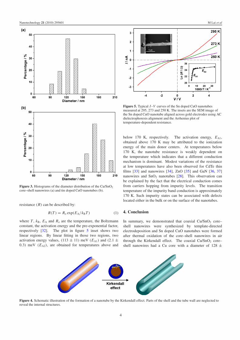
The electrical properties of the Sn doped CuO nanotubeswere investigated by performing I –V measurements at a seriesof temperatures from 30 to 295 K. Three typical I –V curvesare displayed in figure 5. The nonlinear curves indicate thatthe electrical characteristics follow Schottky barriers betweenthe Sn doped CuO nanotube and Au electrodes. The resistivityof the nanotubes is approximately (870 ± 85) � cm in air at295 K. The Arrhenius plot of TCR of the nanotubes is shownin figure 5 inset. For semiconducting materials, the electrical
3
Nanotechnology 21 (2010) 295601 M Lai et al
Figure 3. Histograms of the diameter distribution of the Cu/SnO2
core–shell nanowires (a) and tin doped CuO nanotubes (b).
resistance (R) can be described by:
R(T ) = Ro exp(EA/kBT ) (1)
where T , kB, EA and Ro are the temperature, the Boltzmannconstant, the activation energy and the pre-exponential factor,respectively [32]. The plot in figure 5 inset shows twolinear regions. By linear fitting in those two regions, twoactivation energy values, (113 ± 11) meV (EA1) and (2.1 ±0.3) meV (EA2), are obtained for temperatures above and
Figure 5. Typical I–V curves of the Sn doped CuO nanotubesmeasured at 295, 273 and 250 K. The insets are the SEM image ofthe Sn doped CuO nanotube aligned across gold electrodes using ACdielectrophoresis alignment and the Arrhenius plot oftemperature-dependent resistance.
below 170 K, respectively. The activation energy, EA1,obtained above 170 K may be attributed to the ionizationenergy of the main donor centers. At temperatures below170 K, the nanotube resistance is weakly dependent onthe temperature which indicates that a different conductionmechanism is dominant. Modest variations of the resistanceat low temperatures have also been observed for CdTe thinfilms [33] and nanowires [34], ZnO [35] and GaN [36, 37]nanowires and SnO2 nanotubes [28]. This observation canbe explained by the fact that the electrical conduction comesfrom carriers hopping from impurity levels. The transitiontemperature of the impurity band conduction is approximately170 K. Such impurity states can be associated with defectslocated either in the bulk or on the surface of the nanotubes.
4. Conclusion
In summary, we demonstrated that coaxial Cu/SnO2 core–shell nanowires were synthesized by template-directedelectrodeposition and Sn doped CuO nanotubes were formedafter thermal oxidation of the core–shell nanowires in airthrough the Kirkendall effect. The coaxial Cu/SnO2 core–shell nanowires had a Cu core with a diameter of 128 ±
Figure 4. Schematic illustration of the formation of a nanotube by the Kirkendall effect. Parts of the shell and the tube wall are neglected toreveal the internal structures.
4

Nanotechnology 21 (2010) 295601 M Lai et al
15 nm and a thin SnO2 shell with a thickness of 13 ±2 nm. The methodology that was demonstrated is verygeneral and it is envisaged that it can be extended to generatecoaxial SnO2-shelled materials with various electrodepositedcores. After thermal oxidation in air, the core–shell nanowireswere oxidized to Sn doped CuO nanotubes with internal andexternal diameters of 69 and 176 nm, respectively. The I –V measurements showed that the resistivity of the nanotubewas 870 � cm in air at 295 K. The temperature dependencyof the electrical resistance was investigated. Two dominantmechanisms were attributed to the electrical conduction aboveand below 170 K, respectively. Sn doped CuO nanotubes mayoffer promising applications in 1D nanostructure-based devicessuch as nano gas sensors.
Acknowledgments
This material is based on research sponsored by the NationalInstitute of Environmental Health Sciences under agreementnumber (grant No. U01ES016026) and National NaturalScience Foundation of China (NSFC, No. 20907021). TheUnited States government is authorized to reproduce anddistribute reprints for government purposes, not withstandingany copyright notation thereon.
References
[1] Jun J, Jin C, Kim H, Park S and Lee C 2009 Appl. Surf. Sci.255 8544
[2] Hao Y and Gong H 2008 Chem. Vapor Depos. 14 9[3] Anandan S, Wen X G and Yang S H 2005 Mater. Chem. Phys.
93 35[4] Wang X, Hu C, Liu H, Du G, He X and Xi Y 2010 Sensors
Actuators B 144 220[5] Aygun S and Cann D 2005 Sensors Actuators B 106 837[6] Li C, Wei W, Fang S, Wang H, Zhang Y, Gui Y and
Chen R 2010 J. Power Sources 195 2939[7] Huang L S, Yang S G, Li T, Gu B X, Du Y W, Lu Y N and
Shi S Z 2004 J. Cryst. Growth 260 130[8] Wang W, Zhan Y, Wang X, Lui Y, Zheng C and Wang G 2002
Mater. Res. Bull. 37 1093[9] Wang H, Xu J Z, Zhu J J and Chen H Y 2002 J. Cryst. Growth
244 88
[10] Xu J F, Ji W, Shen Z X, Tang S H, Ye X R, Jia D Z andXin X Q 1999 J. Solid State Chem. 147 516
[11] Xu G, Liu Y, Xu G and Wang G 2002 Mater. Res. Bull.37 2365
[12] Yu T, Zhao X, Shen Z X, Wu Y H and Su W H 2004 J. Cryst.Growth 268 590
[13] Jiang X C, Herricks T and Xia Y N 2002 Nano Lett. 2 1333[14] Xu C H, Woo C H and Shi S Q 2004 Chem. Phys. Lett. 399 62[15] Baek K-K and Tuller H L 1993 Sensors Actuators B 13 238[16] Hung C-M 2009 Power Technol. 196 56[17] Yu J H and Choi G M 2001 Sensors Actuators B 75 56[18] Prabhakaran D and Boothroyd A T 2003 J. Cryst. Growth
250 77[19] Yin Y, Rioux R M, Erdonmez C K, Hughes S, Somorjai G A
and Alivisatos A P 2004 Science 304 711[20] Fan H J, Gosele U and Zacharias M 2007 Small 3 1660[21] Sun Y and Xia Y 2002 Science 298 2176[22] Gao J H, Zhang B, Zhang X X and Xu B 2006 Angew. Chem.
Int. Edn 45 1220[23] Wang Y, Cai L and Xia Y 2005 Adv. Mater. 17 473[24] Fan H J, Knez M, Scholz R, Nielsch K, Pippel E, Hesse D,
Zacharias M and Gosele U 2006 Nat. Mater. 5 627[25] Zhou J, Liu J, Wang X D, Song J H, Tummala R, Xu N S and
Wang Z L 2007 Small 3 622[26] Yin Y, Erdonmez C K, Cabot A, Hughes S and Alivisatos A P
2006 Adv. Funct. Mater. 16 1389[27] Prasad S and Paul A 2007 Appl. Phys. Lett. 90 233114[28] Lai M, Lim J-H, Mubeen S, Rheem Y, Mulchandani A,
Deshusses M A and Myung N V 2009 Nanotechnology20 185602
[29] Lim J H, Phiboolsirichit N, Mubeen S, Rheem Y,Deshusses M A, Mulchandani A and Myung N V 2010Electroanalysis 22 99
[30] Lai M, Martinez J A G, Gratzel M and Riley D J 2006 J. Mater.Chem. 16 2843
[31] Nakamura R, Tokozakura D, Nakajima H, Lee J G andMori H 2007 J. Appl. Phys. 101 074303
[32] Willams W 1902 Phil. Mag. Series 6 3 515[33] Moesslein J, Lopez-Otero A, Fehrenbruch A, Kim D and
Bube R H 1993 J. Appl. Phys. 73 8359[34] Kum M C, Yoo B Y, Rheem Y W, Bozhilov K N, Chen W,
Mulchandani A and Myung N V 2008 Nanotechnology19 325711
[35] Tazlaoanu C, Ion L, Enculescu I, Sima M, Enculescu M,Matei E, Neumann R, Bazavan R, Bazavan D andAntohe S 2008 Physica E 40 2504
[36] Simpkins B S, Pehrsson P E and Laracuente A R 2006 Appl.Phys. Lett. 88 072111
[37] Motayed A, Davydov A V, Mohammad S N andMelngailis J 2008 J. Appl. Phys. 104 024302
5


![Iron-doped TiO2 Catalysts with Photocatalytic Activity · ZnO, CuO, TiO 2 and Ag [9,22-24]. The solid-state molten salt method is an easy, fast and inexpensive approach to provide](https://static.fdocuments.in/doc/165x107/5ec172b4d6a24453123925fa/iron-doped-tio2-catalysts-with-photocatalytic-zno-cuo-tio-2-and-ag-922-24.jpg)