Synthesis and Timing (Verilog)users.wpi.edu/~rjduck/Synthesis and Timing module 11 rev a.pdf · Jim...
28
Jim Duckworth, WPI Synthesis and Timing - Module 11 1 Synthesis and Timing (Verilog) Module 11
Transcript of Synthesis and Timing (Verilog)users.wpi.edu/~rjduck/Synthesis and Timing module 11 rev a.pdf · Jim...

Jim Duckworth, WPI Synthesis and Timing - Module 111
Synthesis and Timing (Verilog)
Module 11

Jim Duckworth, WPI Synthesis and Timing - Module 112
Overview
• Metastability
• Constraints
• Clock Skew
• Clock Domains
– Core Generator

Jim Duckworth, WPI Synthesis and Timing - Module 113
Metastability
• Flip-flops may go metastable if input signals do not meet
setup and hold specifications relative to clock signal
• Rules:
– Input only drives one FF, Add 2-FF synchronizer
always @ (posedge clk)
begin
inp_d <= inp;
inp_dd <= inp_d;
end
CLK
D
Q

Jim Duckworth, WPI Synthesis and Timing - Module 114
Creating one clk pulse synchronizer
• Sometimes an input signal is asynchronous and much longer than clock period
• Add 3FF synchronizer and generate single pulse
always @ (posedge clk)
begin
inp_d <= inp;
inp_dd <= inp_d;
inp_ddd <= inp_dd;
inp_pulse <= inp_dd & ~inp_ddd;

Jim Duckworth, WPI Synthesis and Timing - Module 115
Timing Constraints
• Used to guide the synthesis tools
• Example 32-bit counter - no constraints (speed grades -4 and -5)======================================================
Advanced HDL Synthesis Report
Macro Statistics
# Counters : 1
32-bit up counter : 1
======================================================
Timing Summary:
---------------
Speed Grade: -4
Minimum period: 6.680ns (Maximum Frequency: 149.703MHz)
Minimum input arrival time before clock: No path found
Maximum output required time after clock: 8.094ns
Maximum combinational path delay: No path found
===============================================
Speed Grade: -5
Minimum period: 5.767ns (Maximum Frequency: 173.400MHz)

Jim Duckworth, WPI Synthesis and Timing - Module 116
Adding timing constraint
• Add to UCF file:– NET "clk" PERIOD = 6ns HIGH 50%;
WARNING:Par:62 - Your design did not meet timing.
-------------------------------------------------------------------------------------------
Constraint | Check | Worst Case | Best Case | Timing |Timing | Slack | Achievable |
Errors | Score
-------------------------------------------------------------------------------------------
* NET "clk_BUFGP/IBUFG" PERIOD = 6 ns HIGH | SETUP| -0.456ns | 6.456ns | 9| 1430
50% | HOLD | 2.432ns | | 0| 0
-------------------------------------------------------------------------------------------
1 constraint not met.
Jim Duckworth, WPI Synthesis and Timing - Module 117
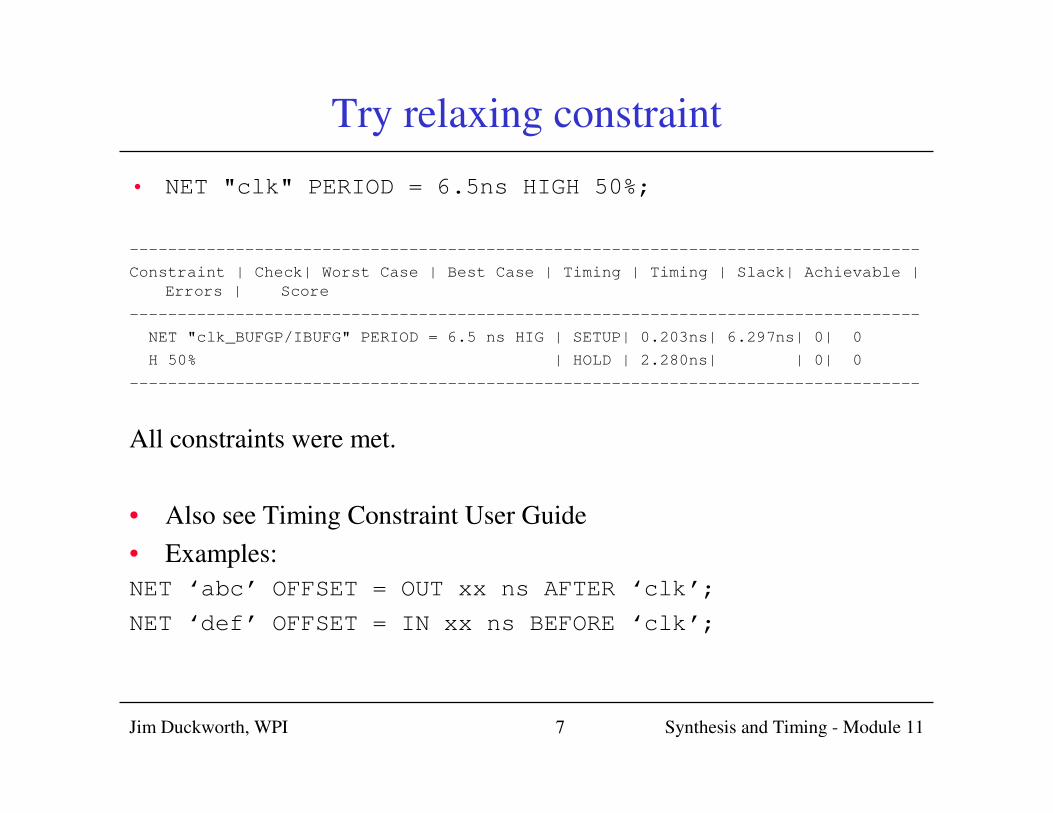
Try relaxing constraint
• NET "clk" PERIOD = 6.5ns HIGH 50%;
----------------------------------------------------------------------------------
Constraint | Check| Worst Case | Best Case | Timing | Timing | Slack| Achievable |
Errors | Score
----------------------------------------------------------------------------------
NET "clk_BUFGP/IBUFG" PERIOD = 6.5 ns HIG | SETUP| 0.203ns| 6.297ns| 0| 0
H 50% | HOLD | 2.280ns| | 0| 0
----------------------------------------------------------------------------------
All constraints were met.
• Also see Timing Constraint User Guide
• Examples:
NET ‘abc’ OFFSET = OUT xx ns AFTER ‘clk’;
NET ‘def’ OFFSET = IN xx ns BEFORE ‘clk’;

Jim Duckworth, WPI Synthesis and Timing - Module 118
Clock Skew
• The difference between the time a clock signal arrives at
the source flip-flop in a path and the time it arrives at the
destination flip-flop.
– Misalignment of clock edges
– Degrades (reduces) time for flip-flop to flip-flop timing
• Can be caused by different things but wire interconnect
delays are the main cause inside FPGAs
– There are fast dedicated clock circuits and slower data paths
Jim Duckworth, WPI Synthesis and Timing - Module 119
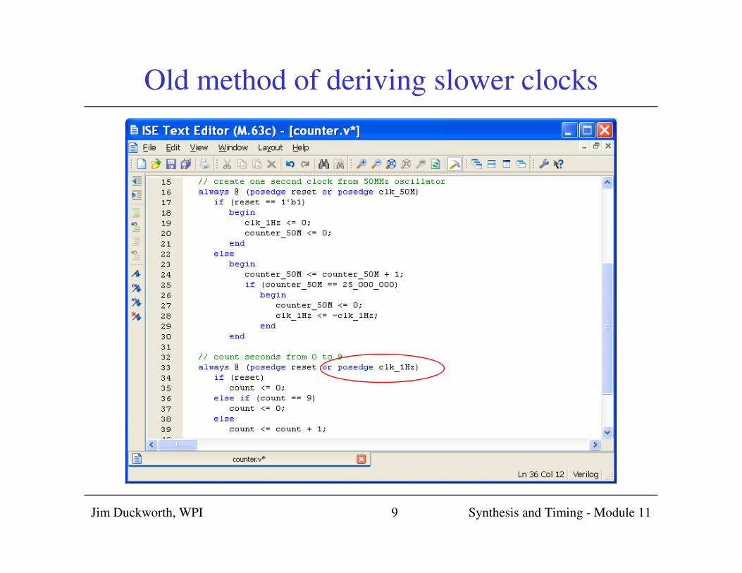
Old method of deriving slower clocks

Jim Duckworth, WPI Synthesis and Timing - Module 1110
WARNING:Route:455 - CLK Net:clk_1Hz may have excessive
skew because 0 CLK pins and 1 NON_CLK pins failed to
route using a CLK template.
Jim Duckworth, WPI Synthesis and Timing - Module 1111
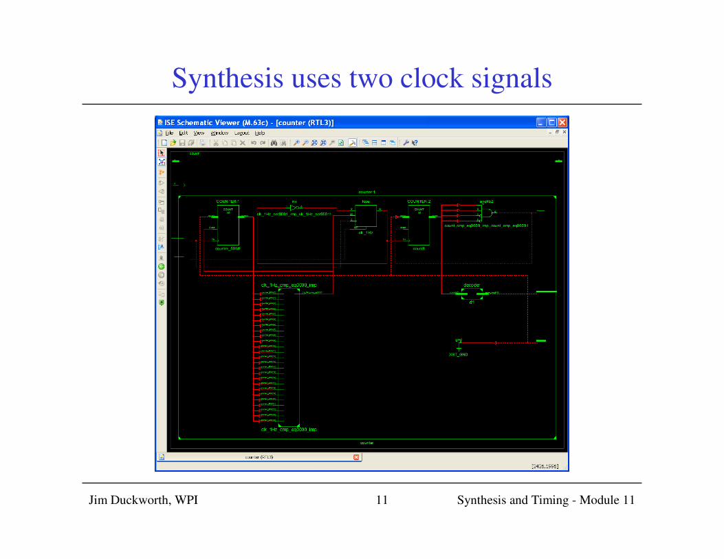
Synthesis uses two clock signals

Jim Duckworth, WPI Synthesis and Timing - Module 1112
Two clock signals – not so good!

Jim Duckworth, WPI Synthesis and Timing - Module 1113
Modify to only use one clock signal

Jim Duckworth, WPI Synthesis and Timing - Module 1114
Clock signals use dedicated lines

Jim Duckworth, WPI Synthesis and Timing - Module 1115
Clock drives all flip-flops

Jim Duckworth, WPI Synthesis and Timing - Module 1116Jim Duckworth, WPI 16
Crossing Clock Domains - FIFO
ADCFIFO
400 MHz
200 MHz
SRAM
FPGA
Jim Duckworth, WPI Synthesis and Timing - Module 1117
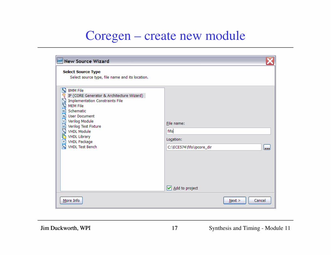
Coregen – create new module
Jim Duckworth, WPI 17

Jim Duckworth, WPI Synthesis and Timing - Module 1118
FIFO Generator
Jim Duckworth, WPI VHDL for Modeling - Module 1018

Jim Duckworth, WPI Synthesis and Timing - Module 1119
Select Options (1 of 6)
Jim Duckworth, WPI 19

Jim Duckworth, WPI Synthesis and Timing - Module 1120
Specifying Write and Read widths
Jim Duckworth, WPI 20
Jim Duckworth, WPI Synthesis and Timing - Module 1121
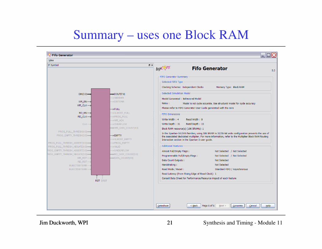
Summary – uses one Block RAM
Jim Duckworth, WPI 21

Jim Duckworth, WPI Synthesis and Timing - Module 1122
Core is added to Project
Jim Duckworth, WPI 22
Jim Duckworth, WPI Synthesis and Timing - Module 1123
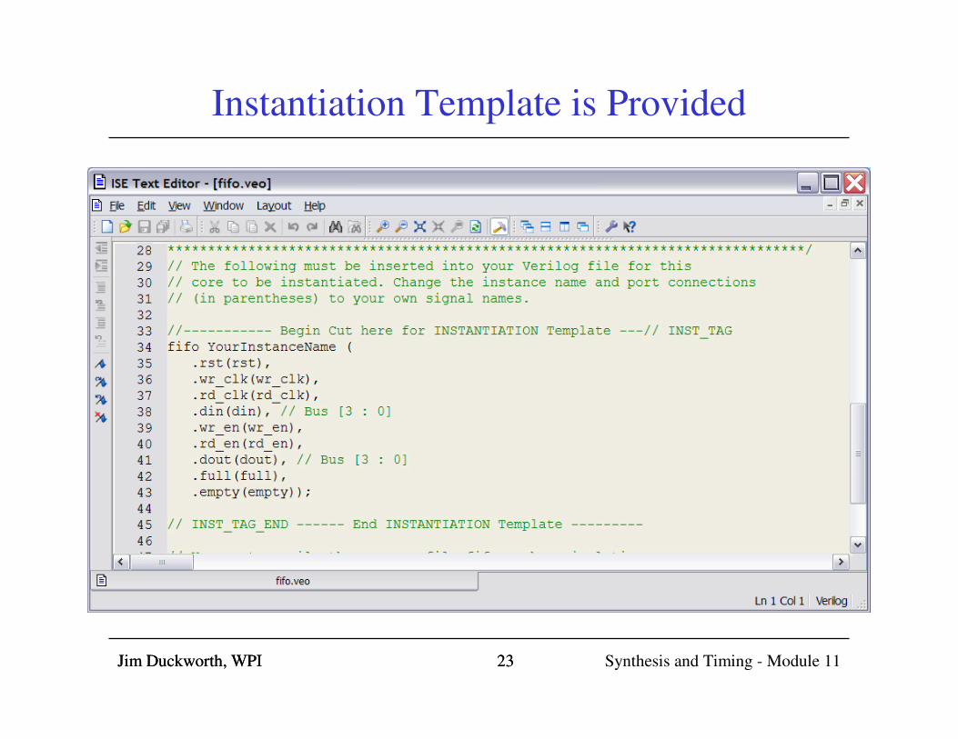
Instantiation Template is Provided
Jim Duckworth, WPI 23

Jim Duckworth, WPI Synthesis and Timing - Module 1124
Simple Top Level to Demonstrate Use
Jim Duckworth, WPI VHDL for Modeling - Module 1024
Jim Duckworth, WPI Synthesis and Timing - Module 1125
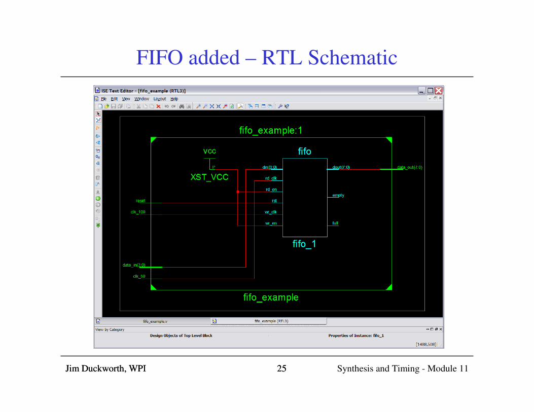
FIFO added – RTL Schematic
Jim Duckworth, WPI 25
Jim Duckworth, WPI Synthesis and Timing - Module 1126
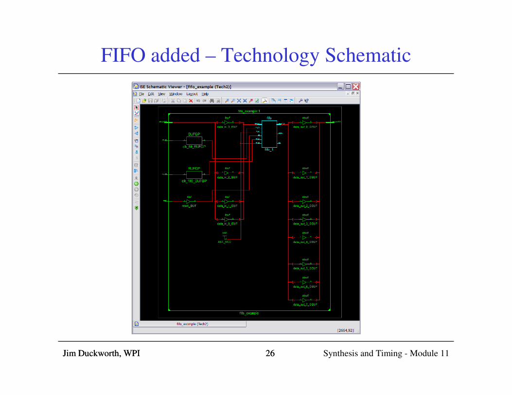
FIFO added – Technology Schematic
Jim Duckworth, WPI 26

Jim Duckworth, WPI Synthesis and Timing - Module 1127
Simple Test Bench to Show Operation
Jim Duckworth, WPI 27
Jim Duckworth, WPI Synthesis and Timing - Module 1128
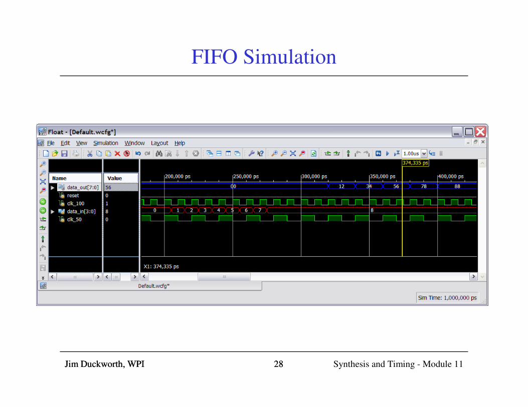
FIFO Simulation
Jim Duckworth, WPI 28