Converting Carbon to useful forms.. Carbon emission in the UK.

IOP PUBLISHING NANOTECHNOLOGY
Nanotechnology 18 (2007) 245603 (5pp) doi:10.1088/0957-4484/18/24/245603
Synthesis and field emission characteristicsof carbon nanocoils with a high aspectratio supported by copper micro-tipsWoo Yong Sung, Jong Girl Ok, Wal Jun Kim, Seung Min Lee,Soon Chang Yeon, Ho Young Lee and Yong Hyup Kim1
School of Mechanical and Aerospace Engineering, Seoul National University, Sillim-dong,Gwanak-gu, Seoul 151-742, Republic of Korea
E-mail: [email protected]
Received 27 February 2007, in final form 30 April 2007Published 18 May 2007Online at stacks.iop.org/Nano/18/245603
AbstractCarbon nanocoils (CNCs) were synthesized via thermal chemical vapourdeposition (CVD) with C2H2 and NH3 gases at 600 ◦C. A Ni catalyst wasplaced upon the copper micro-tip structures that were fabricated on a siliconsubstrate. Our CNCs had a long rope shape with a length not exceeding100 μm and a nanoscale diameter. The copper micro-tips were formedthrough high current pulse electroplating, which played a significant role incharacterizing our CNCs. The CNCs grown on the copper micro-tips showedoutstanding field emission performance and long-term stability. Their turn-onfield, defined as that at a current density of 10 μA cm−2, was 1.30 V μm−1
and the maximum current density reached 11.17 mA cm−2 at an electric fieldof 2.39 V μm−1.
1. Introduction
Since the discovery of carbon nanotubes (CNTs) by Iijima [1],there has been great interest in the physical, chemical andelectromechanical properties of carbon-based nanomaterialsincluding coiled carbon nanofibres [2–5] and carbon nanocoils(CNCs) [6, 7]. The synthesis conditions of CNCs withspecific catalysts [8–11] as well as analytical research havebeen intensively investigated [12]. Wen et al [13] suggesteda three-dimensional model for the growth mechanism of coiledcarbon nanofibres with respect to three contiguous crystalplanes. Xie et al [14] explained that coiled nanotubes involveperiodic insertion of pentagonal–heptagonal ‘defect’ pairs intothe hexagonal network on the wall. Pan et al [15] showed thatthe uneven speed of carbon extrusion at different parts of thecatalyst grain leads to the helical growth of coils. Bai et al [16]reported pure coiled carbon nanostructures synthesized by thecatalytic decomposition of acetylene on an alumina support.Huang et al [17] synthesized CNCs on silicon substrates havinga concave–convex surface morphology made by hydrofluoricacid (HF) erosion. Another method for synthesizing CNCs waspresented by Motojima and colleagues [18], who introduced
1 Author to whom any correspondence should be addressed[1] .
acetylene pyrolysis at 740–770 ◦C using Ni powder as thecatalyst. They applied an external magnetic field to thereaction zone, which was similar to the micro-coil preparationreactor. It was proposed that the application of a magneticfield considerably suppressed the sintering of fine Ni powder,which led Ni particles to become nanosized. Meanwhile,the field emission characteristics of CNCs have also beenwidely examined. Pan et al [19] demonstrated a high emissioncurrent density, excellent stability and good uniformity of CNCemitters prepared by the catalytic thermal decomposition ofacetylene pyrolysis at 700 ◦C. Jiang et al [20] reported oncoiled CNTs synthesized by plasma enhanced CVD (PECVD)using a C2H2–H2 gas mixture and their field emissioncharacteristics.
In the present study, we synthesized CNCs upon coppermicro-tips by thermal CVD at 600 ◦C, which is low enoughto utilize glass substrates, and investigated their properties aswell as their field emission characteristics. The copper micro-tips were fabricated using high current pulse electroplating,and had a very sharp appearance as shown in figure 1. Thisparticular substrate morphology with the copper micro-tipsallows our CNCs to have a remarkable growth feature: theinterspace of the micro-tips seems to accelerate the growth rate
0957-4484/07/245603+05$30.00 1 © 2007 IOP Publishing Ltd Printed in the UK
Nanotechnology 18 (2007) 245603 W Y Sung et al
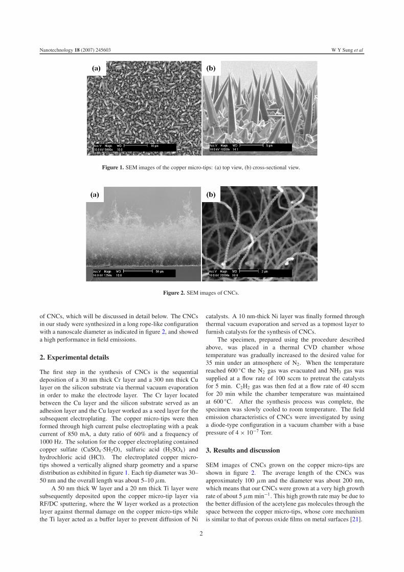
Figure 1. SEM images of the copper micro-tips: (a) top view, (b) cross-sectional view.
Figure 2. SEM images of CNCs.
of CNCs, which will be discussed in detail below. The CNCsin our study were synthesized in a long rope-like configurationwith a nanoscale diameter as indicated in figure 2, and showeda high performance in field emissions.
2. Experimental details
The first step in the synthesis of CNCs is the sequentialdeposition of a 30 nm thick Cr layer and a 300 nm thick Culayer on the silicon substrate via thermal vacuum evaporationin order to make the electrode layer. The Cr layer locatedbetween the Cu layer and the silicon substrate served as anadhesion layer and the Cu layer worked as a seed layer for thesubsequent electroplating. The copper micro-tips were thenformed through high current pulse electroplating with a peakcurrent of 850 mA, a duty ratio of 60% and a frequency of1000 Hz. The solution for the copper electroplating containedcopper sulfate (CuSO4·5H2O), sulfuric acid (H2SO4) andhydrochloric acid (HCl). The electroplated copper micro-tips showed a vertically aligned sharp geometry and a sparsedistribution as exhibited in figure 1. Each tip diameter was 30–50 nm and the overall length was about 5–10 μm.
A 50 nm thick W layer and a 20 nm thick Ti layer weresubsequently deposited upon the copper micro-tip layer viaRF/DC sputtering, where the W layer worked as a protectionlayer against thermal damage on the copper micro-tips whilethe Ti layer acted as a buffer layer to prevent diffusion of Ni
catalysts. A 10 nm-thick Ni layer was finally formed throughthermal vacuum evaporation and served as a topmost layer tofurnish catalysts for the synthesis of CNCs.
The specimen, prepared using the procedure describedabove, was placed in a thermal CVD chamber whosetemperature was gradually increased to the desired value for35 min under an atmosphere of N2. When the temperaturereached 600 ◦C the N2 gas was evacuated and NH3 gas wassupplied at a flow rate of 100 sccm to pretreat the catalystsfor 5 min. C2H2 gas was then fed at a flow rate of 40 sccmfor 20 min while the chamber temperature was maintainedat 600 ◦C. After the synthesis process was complete, thespecimen was slowly cooled to room temperature. The fieldemission characteristics of CNCs were investigated by usinga diode-type configuration in a vacuum chamber with a basepressure of 4 × 10⁻⁷ Torr.
3. Results and discussion
SEM images of CNCs grown on the copper micro-tips areshown in figure 2. The average length of the CNCs wasapproximately 100 μm and the diameter was about 200 nm,which means that our CNCs were grown at a very high growthrate of about 5 μm min−1. This high growth rate may be due tothe better diffusion of the acetylene gas molecules through thespace between the copper micro-tips, whose core mechanismis similar to that of porous oxide films on metal surfaces [21].
2

Nanotechnology 18 (2007) 245603 W Y Sung et al
Figure 3. HR-TEM image of CNCs.
Figure 3 is an HR-TEM image of an individual strand ofCNCs grown on copper micro-tips, which reveals the typicalnanocoil geometry. Amelinckx et al proposed that one ofthe plausible growth mechanisms of coiled nanostructures isbased on the asymmetric growth rate [22], i.e. inhomogeneousgrowth rates at different parts of the catalyst particles. Ourstudy maintains that the nanoparticles of the Ni catalystswere asymmetrically formed by means of very rough basestructures during the pretreatment process that affected thespecific growth characteristics of the CNCs.
Another possibility is the mobility of carbon atoms thataffect the growth mechanism of CNCs. While nanostructuresamples synthesized under very high temperatures (such as inarc discharge or laser ablation) contain only straight types [23],it is probable that the moderate mobility of carbon atoms dueto the relatively low growth temperature of our study causesthe coiled nanostructure morphology (figure 4).
Figure 4 clearly displays the morphological differencesbetween carbon nanostructures synthesized at differenttemperatures. Although grown on the same base of coppermicro-tips, long CNCs with a larger diameter were grown at600 ◦C while entangled carbon nanostructures with a relativelysmall diameter were formed at 700 ◦C and a mixture of CNCsand fine carbon nanostructures was observed at 650 ◦C.
In brief, the kinetic characteristics of carbon atomsare dependent on the growth temperature as well as the
Figure 5. Raman spectra of the CNCs.
geometrical irregularity of the catalytic particles created bythe characteristic substrate of copper micro-tips and play animportant role in the nanostructure growth mechanism.
The crystalline properties of CNCs grown on coppermicro-tips were inspected via Raman spectral analysis with anexcitation laser wavelength of 514.53 nm. Figure 5 illustratesthe results of Raman spectra measured in the frequency range1100–1700 cm−1. The relative intensity ratio of the D-bandto the G-band (ID/IG) was 0.92, indicating lower crystallinity,which is similar to that of the regular CNTs grown without anelectric field as reported in [24].
The field emission characteristics of the CNCs wereinvestigated by using a diode-type configuration in a vacuumchamber with a base pressure of 4 × 10⁻⁷ Torr. The CNC filmspecimen and a phosphor-coated indium-tin oxide (ITO) glasswere used as the cathode and anode, respectively, where thegap between the cathode and the anode was set to 610 μm.The emission current density was evaluated by averaging themeasured currents over the area of a 6 mm diameter hole.The specimens were aged to remove contaminants and allowedto degas before taking reliability measurements. The fieldemission measurements were carried out several times whileeach of the results was recorded using LABVIEW. Figure 6demonstrates the field emission characteristics of CNCs grownon copper micro-tips. The turn-on field, defined as the value of
Figure 4. SEM images of carbon nanostructures synthesized at the various growth temperatures: (a) 600 ◦C, (b) 650 ◦C, (c) 700 ◦C.
3

Nanotechnology 18 (2007) 245603 W Y Sung et al
0.0008
Ln(I
/V2 )
–22
–20
–18
–16
–14
–12
0.0010 0.0012 0.00141/V
0.0016
Figure 6. Current–voltage (I –V ) curve and Fowler–Nordheim (F–N)plot of CNCs grown on the copper micro-tips.
the applied electric field at a current density of 10 μA cm−2,was only 1.30 V μm−1, which is quite low. The maximumcurrent density of our CNCs was 11.17 mA cm−2 in an electricfield of 2.39 V μm−1. This distinguishing characteristic ofhigh current density could lead to the use of our CNCs inhigh current source applications including x-ray generatorsand microwave devices. The inset of figure 6 indicates theFowler–Nordheim (F–N) plot for the CNCs; it is obviousthat our emission results agree well with the theoretical F–N nature. The field-enhancement factor β of the emitter canbe evaluated from the well-known equation β = −Bφ3/2d/S,where B = 6.83 × 10⁹ (V eV−3/2 m−1), φ is a work function,d is the distance between the emitter tip and the anode, and Sis the slope of the F–N plot [25]. The slope of the F–N plot isdifferent in the low and high electric field regions, as revealedin figure 6. The slope of the F–N plot is steeper in the lowfield region than the high field region. Such a deviation of F–N behaviour caused by the current saturation effect might beattributed to the detachment of adsorbates [26]. The adsorptivegas molecules enhanced the field emission current of CNCs inthe low electric field range. When the current density grew asthe electric field increased, the tip temperature of the CNCsrose via Joule heating, which resulted in the desorption ofadsorbates on the CNCs and led to current saturation. Weworked out β in both the low and high field regimes andfound it to be about 2438 and 6430, respectively, where thework function φ was assumed to be 5 eV. These values canbe favourably compared with the previously reported values,which are in the range of 200–5000 [19]. From the interceptsand slopes of the F–N plots we estimated that the total realemitting area was 2.217 × 10⁻⁹ cm2 for our CNCs. The actualemitting area of CNCs is larger than that of CNTs in otherworks because CNCs have a larger surface area due to theircharacteristic morphology [27] and field emission can occur atthe side of the CNCs [28].
Our CNCs had a long emission lifetime. Figure 7represents the emission current stability over the test periodof 30 h at the direct current (DC) field of 1.64 V μm−1. Theemission current has a maximal drift of 11.3% over 30 h.After the initial 6 h, the emission current did not degrade
0 5 10 15 20 25 300.0
0.2
0.4
0.6
0.8
1.0
1.2
Cu
rren
t d
ensi
ty (
mA
/ cm
2 )
Time (hour)
Carbon nanocoilsIaverage
0.729mAStandard deviation +/- 0.0215mAfluctuation=2.95%
Figure 7. Time dependence of the emission current density of CNCs.
Figure 8. Emission image of CNC emitters at an applied field of2.2 V μm−1.
(This figure is in colour only in the electronic version)
significantly over a continuous 24 h period. The averageemission current Iaverage, standard deviation �I and fluctuationf = �I/Iaverage were determined for the studied CNCs. TheCNCs exhibited fluctuations of 2.95%.
Figure 8 displays a field emission image of the CNCsgrown on copper micro-tips in a vacuum chamber. It wasobserved that our CNCs supported a uniform distribution ofemission sites as well as a stable emission feature.
4. Conclusion
In summary, we synthesized CNCs upon copper micro-tips byusing thermal CVD at 600 ◦C. The copper micro-tips wereformed through high current pulse electroplating, and theirgeometry was very sharp. It is believed that the characteristicsof our CNCs originated from not only inhomogeneous growthrates due to asymmetric catalyst formation guided by thecopper micro-tips during the pretreatment process, but alsoa specific mobility of carbon atoms due to the low growthtemperature. Furthermore, good diffusion of acetylene gasmolecules through the spaces among the copper micro-tips
4

Nanotechnology 18 (2007) 245603 W Y Sung et al
contributed to the high growth rate of CNCs. Our CNCs grownon copper micro-tips showed excellent performance in fieldemission as well as good uniformity and stability. Moreover,the very regular configurations of our CNCs, whose pitch andcoil diameter are uniform, promise further applications in suchfields as nanoelectronics and nanomechanics.
Acknowledgments
This work was supported by a grant (code no 06K1501-01210)from ‘Center for Nanostructured Materials Technology’ under‘21st Century Frontier R&D Programs’ of the Ministry ofScience and Technology, and the Brain Korea 21 Project in2006, Korea.
References
[1] Iijima S 1991 Nature 354 56[2] Motojima S and Chen Q Q 1999 J. Appl. Phys. 85 3919[3] Fonseca A, Hernadi K, Nagy J B, Lambin Ph and Lucas A A
1996 Synth. Met. 77 235[4] Fonseca A, Hernadi K, Nagy J B, Lambin Ph and Lucas A A
1995 Carbon 33 1759[5] Du J H, Su G, Bai S, Sun C and Cheng H M 2001 Sci. China E
44 376[6] Tanaka K, Yoshimura M, Okamoto A and Ueda K 2005 Japan.
J. Appl. Phys. 44 L1158[7] Lau K T, Lu M and Hui D 2006 Composites B 37 437[8] Lu M, Li H L and Lau K T 2004 J. Phys. Chem. B 108 6186[9] Hou H Q, Jun Z, Weller F and Greiner A 2003 Chem. Mater.
15 3170
[10] Xu G, Chen B, Shiki H, Katsumata T, Takikawa H,Sakakibara T, Itoh S and Ina T 2005 Japan. J. Appl. Phys.44 1569
[11] Qin Y, Yu L Y, Wang Y, Li G C and Cui Z L 2006 Solid StateCommun. 138 5
[12] Qin Y, Jiang X and Cui Z L 2005 J. Phys. Chem. B 109 21749[13] Wen Y K and Shen Z M 2001 Carbon 39 2369[14] Xie J, Mukhopadyay K, Yadev J and Varadan V K 2003 Smart
Mater. Struct. 12 744[15] Pan L J, Mei Z and Yoshikazu N 2002 J. Appl. Phys.
91 10058[16] Bai J B 2003 Mater. Lett. 57 2629[17] Huang Z Y, Chen X, Haung J R, Li M Q and Liu J H 2006
Mater. Lett. 60 2073[18] Kuzuya C, Hwang W, Hirako S, Hishikawa Y and
Motojima S 2002 Chem. Vapor. Depos. 8 57[19] Pan L, Hayashida T, Zhang M and Nakayama Y 2001 Japan. J.
Appl. Phys. 40 L235[20] Jiang J, Feng T, Cheng X H, Dai L J, Cao G B, Zhang J H,
Jiang B Y, Wang X, Liu X H and Zou S C 2006 Mater. Lett.60 1085
[21] Shoushan F, Michael G C, Nathan R F, Thomas W T, Alan M Cand Hongjie D 1999 Science 283 512
[22] Amelinckx S, Zhang X B, Bernaerts D, Zhang X F,Ivanov V and Nagy J B 1994 Science 265 635
[23] Cheng J, Zhang X, Tu J, Tao X, Ye Y and Liu F 2006 Mater.Chem. Phys. 95 12
[24] Bao Q and Pan C 2006 Nanotechnology 17 1016[25] Choi J H, Choi S H, Han J H, Yoo J B, Park C Y, Jung T,
Yu S G, Han I T and Kim J M 2003 J. Appl. Phys. 94 487[26] Dean K A and Chalamala B R 2000 Appl. Phys. Lett. 76 375[27] Zeng B, Xiong G Y, Chen S, Wang W Z and Ren Z F 2006
Appl. Phys. Lett. 89 223119[28] Pan L, Konish Y, Tanaka H, Suekane O, Nosaka T and
Nakayama Y 2005 Japan. J. Appl. Phys. 44 1652
5