SYNTHESIS AND CHARACTERIZATION OF ZINC OXIDE/COPPER OXIDE DEPOSITION MUHAMMAD ARIF...
43
SYNTHESIS AND CHARACTERIZATION OF ZINC OXIDE/COPPER OXIDE CORE-SHELL HETEROJUNCTION NANOWIRES GROWN BY VAPOR DEPOSITION MUHAMMAD ARIF KHAN A thesis submitted in fulfilment of the requirements for the award of the degree of Doctor of Philosophy (Physics) Faculty of Science Universiti Teknologi Malaysia AUGUST 2017
Transcript of SYNTHESIS AND CHARACTERIZATION OF ZINC OXIDE/COPPER OXIDE DEPOSITION MUHAMMAD ARIF...
SYNTHESIS AND CHARACTERIZATION OF ZINC OXIDE/COPPER OXIDE
CORE-SHELL HETEROJUNCTION NANOWIRES GROWN BY VAPOR
DEPOSITION
MUHAMMAD ARIF KHAN
A thesis submitted in fulfilment of the
requirements for the award of the degree of
Doctor of Philosophy (Physics)
Faculty of Science
Universiti Teknologi Malaysia
AUGUST 2017

iii
DEDICATION
Specially dedicated to my beloved parents, my fam ily and my friends fo r their
patience, support, prayers, encouragement, and blessings.

iv
ACKNOWLEDGEMENT
First of all, I would like to praise and thank almighty Allah who enabled me
to complete my doctorate. I thank to almighty Allah for making my dream come true.
The day that I dreamt of has finally come and I am graduating my PhD.
I feel honored of being supervised by Prof. Yussof Wahab and Prof.
Samsudi Sakrani. This thesis would not have been completed without their help,
support and guidance. I would like to offer my sincerest gratitude and thanks to both
of my supervisors who have supported me throughout my PhD studies with his
patience and knowledge. Indeed, it was a great privilege to work together as a team.
I would like to express my thanks to UTM for providing me with the support
of best experimental facilities needed to complete my experimental research work
and thesis. My appreciation also goes to all the lecturers and laboratory officers at the
Department of physics, Centre for Sustainable Nanomaterial (CSNano) Ibnu Sina
Institute for Scientific and Industrial Research, and University Laboratory
Management Unit (UPMU) of UTM.
I am grateful to my family, parents and parents-in-law for all their love and
encouragement. They raised me with love and supported me in all my pursuits. They
have been a constant source of inspiration throughout my life. I will forever be
indebted to all of them for their support, encouragement and invaluable prayers.
The last but not the least heartfelt acknowledgment must go to my wife and
my lovely daughter Honey. Their love, support, encouragement and patience has
helped me massively throughout this period.
v
ABSTRACT
This thesis investigates the controlled growth and vertically aligned ZnO/CuO core-shell heterojunction nanowires (NWs) formation by vapor deposition and oxidation approach. ZnO/CuO heterostructure nanowires were grown on n-type Si substrate using modified thermal chemical vapor deposition (TCVD) assisted by sputtering deposition followed by thermal oxidation under controlled growth conditions. The effects of fabrication parameters on structure, growth mechanism, optical and electrical properties of the ZnO/CuO core-shell heterojunction were thoroughly investigated. Structural characterization by field emission scanning electron microscope (FESEM), high resolution transmission electron microscope (HR-TEM), scanning transmission electron microscope (STEM), X-ray photoelectron spectroscope (XPS), X-ray diffractometer (XRD) and energy dispersive X-ray (EDX) reveals that a highly pure crystalline ZnO core and polycrystalline CuO shell were successfully fabricated in which ZnO and CuO are of hexagonal wurtzite and monoclinic structures, respectively. The growth of ZnO nanowires is along the c-axis [002] direction and the nanowires have relatively smooth surfaces with diameters in the range of 35-45 nm and lengths in the range of 700-1300 nm. The CuO nanoshell with thickness of around 8-10 nm is constructed of nanocrystals with sizes in the range of 3-10 nm. EDX spectrum, elemental mapping and high angle annular dark field (HAADF) STEM confirmed that the NW compositions were Zn, Cu and O. Photoluminescence (PL) study shows the enhancement of intensity ratio and decrease in the energy band of ZnO/CuO coreshell heterojunction NW arrays that might be very useful in photocatalysis, light emission devices and solar energy conversion applications. Similarly, UV-VIS-NIR spectroscopy study shows that the grown ZnO NW arrays have a maximum reflectance of approximately 42% in the 200 to 800 nm range while the ZnO/CuO core-shell heterojunction NW arrays have a decreased value of 24%. This means that the absorption efficiency of ZnO/CuO core-shell heterojunction nanowire arrays clearly shows a higher absorption compared to pure ZnO nanowire arrays. Besides, the good rectifying behavior of ZnO/CuO core-shall NW by conductive AFM (C- AFM) showed that p-n junction was successfully fabricated. Furthermore, from the XPS analysis, the measured values for valence band offset (VBO) and conduction band offset (CBO) were found to be 2.4 eV and 0.23 eV, respectively for the fabrication of ZnO/CuO core-shell heterojunction NWs. It was observed that ZnO/CuO core-shell heterojunction NWs have type-II band alignment. This study obviously suggests that using the controlled growth mechanism, it is possible to control crystal structure, surface morphologies and orientation of the core-shell NW arrays.

vi
ABSTRAK
Tesis ini menyiasat pertumbuhan terkawal dan pembentukan teras-petala simpangan hetero dawai nano (NW) ZnO/CuO jajaran menegak dengan pendekatan pemendapan wap dan pengoksidaan. Dawai nano struktur hetero ZnO/CuO ditumbuhkan di atas substrat Si jenis-n nenggunakan pemendapan terma wap kimia (TCVD) yang diubah suai dibantu oleh pemendapan percikan diikuti dengan pengoksidaan terma di bawah keadaan pertumbuhan terkawal. Kesan parameter fabrikasi terhadap struktur, mekanisme pertumbuhan dan sifat-sifat optik dan elektrik bagi teras-petala simpangan hetero ZnO/CuO telah disiasat dengan menyeluruh. Pencirian struktur dengan mikroskop elektron pengimbas pemancaran medan (FESEM), mikroskop elektron penghantaran resolusi tinggi (HRTEM), mikroskop elektron penghantaran imbasan (STEM), spektroskop fotoelektron sinar-X (XPS), pembelau sinar-X (XRD) dan spektroskop serakan tenaga sinar-X (EDX) menunjukkan bahawa kristal teras ZnO yang sangat tulen dan polihabluran petala CuO telah berjaya difabrikasi di mana ZnO dan CuO masing-masing adalah berstruktur heksagon wurtzite dan monoklinik. Pertumbuhan dawai nano ZnO adalah sepanjang arah paksi-c [002] dan dawai nano mempunyai permukaan yang licin dengan diameter dalam julat 35-45 nm dan dan panjang dalam julat 700-1300 nm. Petala nano CuO dengan ketebalan sekitar 8-10 nm dibina daripada nanokristal dengan saiz dalam julat 3-10 nm. Spektrum EDX, STEM pemetaan unsur dan anulus medan gelap bersudut tinggi (HAADF) dan STEM mengesahkan bahawa komposisi NW ialah Zn, Cu dan O. Kajian photoluminescence (PL) menunjukkan peningkatan nisbah keamatan dan pengurangan jalur tenaga tatasusunan NW simpangan hetero teras-petala ZnO/CuO yang berkemungkinan sangat berguna dalam aplikasi fotomangkin, peranti pemancar cahaya dan penukaran tenaga solar. Begitu juga, spektroskopi UV-VIS-NIR menunjukkan bahawa tatasusunan NW ZnO yang ditumbuhkan menghasilkan pantulan maksimum kira-kira 42% dalam julat 200-800 nm manakala tatasusunan NW simpangan hetero teras-petala ZnO/CuO telah berkurangan kepada 24%. Ini bermakna tatasusunan NW simpangan hetero teras- petala ZnO/CuO menunjukkan kecekapan penyerapan lebih tinggi berbanding tatasusunan NW ZnO tulen. Selain itu, sifat membetulkan NW teras-petala ZnO/CuO yang baik menunjukkan yang persimpangan p-n telah berjaya difabrikasi. Tambahan pula, dari analisis XPS, telah ditemui nilai diukur bagi ofset jalur valens (VBO) dan ofset jalur konduksi (CBO) masing-masing ialah 2.4 eV dan 0.23 eV, untuk fabrikasi NW simpangan hetero teras-petala ZnO/CuO. Didapati bahawa penjajaran jalur bagi NW simpangan hetero teras-petala ZnO/CuO adalah jenis-II. Kajian ini jelas menunjukkan bahawa dengan menggunakan mekanisme pertumbuhan dikawal, terdapat kemungkinan untuk mengawal struktur kristal, morfologi permukaan dan orientasi teras-petala tatasusunan NW.
vii
TABLE OF CONTENTS
CHAPTER TITLE PAGE
DECLARATION ii
DEDICATION iii
ACKNOWLEDGEMNET iv
ABSTRACT v
ABSTRAK vi
TABLE OF CONTENTS vii
LIST OF TABLES xi
LIST OF FIGURES xii
LIST OF ABBREVIATIONS xviii
LIST OF SYMBOLS xix
LIST OF APPENDICES xx
1 INTRODUCTION 1
1.1 Background 1
1.2 Problem Statement 4
1.3 Research Objectives 6
1.4 Scope of the Study 6
1.5 Significance of the Study 8
1.6 Organization of Thesis 8
2 LITERATURE REVIEW 10
2.1 Introduction 10
2.2 ZnO/CuO Heterostructure Nanowires 10
2.3 Zinc Oxide Material Properties 14
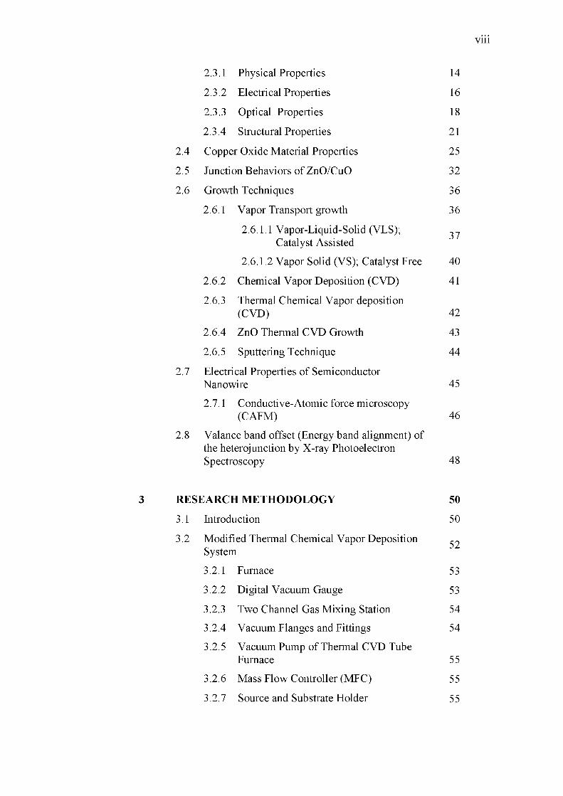
viii
2.3.1 Physical Properties 14
2.3.2 Electrical Properties 16
2.3.3 Optical Properties 18
2.3.4 Structural Properties 21
2.4 Copper Oxide Material Properties 25
2.5 Junction Behaviors of ZnO/CuO 32
2.6 Growth Techniques 36
2.6.1 Vapor Transport growth 36
2.6.1.1 Vapor-Liquid-Solid (VLS); ^Catalyst Assisted 3 7
2.6.1.2 Vapor Solid (VS); Catalyst Free 40
2.6.2 Chemical Vapor Deposition (CVD) 41
2.6.3 Thermal Chemical Vapor deposition(CVD) 42
2.6.4 ZnO Thermal CVD Growth 43
2.6.5 Sputtering Technique 44
2.7 Electrical Properties of SemiconductorNanowire 45
2.7.1 Conductive-Atomic force microscopy(CAFM) 46
2.8 Valance band offset (Energy band alignment) ofthe heterojunction by X-ray Photoelectron Spectroscopy 48
3 RESEARCH METHODOLOGY 50
3 .1 Introduction 50
3.2 Modified Thermal Chemical Vapor DepositionSystem 52
3.2.1 Furnace 53
3.2.2 Digital Vacuum Gauge 53
3.2.3 Two Channel Gas Mixing Station 54
3.2.4 Vacuum Flanges and Fittings 54
3.2.5 Vacuum Pump of Thermal CVD TubeFurnace 55
3.2.6 Mass Flow Controller (MFC) 55
3.2.7 Source and Substrate Holder 55
ix
3.2.8 Gas Supply Systems 56
3.3 Substrate Preparation 56
3.3.1 Substrate Cutting 57
3.3.2 Cleaning of Substrate 57
3.4 Synthesis of ZnO Nanowire by Thermal CVD 58
3.5 Synthesis of CuO Nanowire by Thermal Oxidation 60
3.6 High Vacuum Dual Target Sputtering System 61
3.7 Growth of ZnO/CuO Core-Shell heterojunction NW Arrays 62
3.8 Characterization Techniques 64
3.8.1 Field emission scanning electron microscope (FE-SEM) 64
3.8.2 Energy dispersive X-ray spectroscopy (EDX) 66
3.8.3 High-resolution transmission electron microscopy (HR-TEM) 67
3.8.4 X-ray photoelectron spectroscopy (XPS) 68
3.8.5 Raman Spectroscopy (RS) 70
3.8.6 X-ray diffraction (XRD) 72
3.8.7 Photoluminescence (PL) 74
3.8.8 UV-VIS NIR Reflectance spectroscopy 75
3.9 Electrical measurement (I-V Characteristic) of heterojunction nanowire by C-AFM 76
RESULTS AND DISCUSSION 78
4.1 Introduction 78
4.2 Structural Characterization of CuO Nanowires 79
4.2.1 Growth parameters of CuO Nanowires 79
4.2.2 Morphological Characteristics and EDXAnalysis 80
4.2.2.1 The effect of oxygen pressure on the formation of CuOnanowires 84
4.2.2.2 The effect of temperature on theformation of CuO nanowires 85
4.2.3 X-ray diffraction analysis of CuO 87
4
x
Nanowires
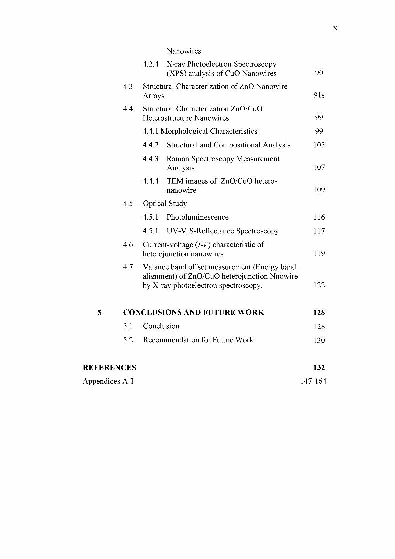
4.2.4 X-ray Photoelectron Spectroscopy(XPS) analysis of CuO Nanowires 90
4.3 Structural Characterization of ZnO NanowireArrays 91s
4.4 Structural Characterization ZnO/CuOHeterostructure Nanowires 99
4.4.1 Morphological Characteristics 99
4.4.2 Structural and Compositional Analysis 105
4.4.3 Raman Spectroscopy MeasurementAnalysis 107
4.4.4 TEM images of ZnO/CuO heteronanowire 109
4.5 Optical Study
4.5.1 Photoluminescence 116
4.5.1 UV-VIS-Reflectance Spectroscopy 117
4.6 Current-voltage (I-V) characteristic ofheterojunction nanowires 119
4.7 Valance band offset measurement (Energy band alignment) of ZnO/CuO heterojunction Nnowireby X-ray photoelectron spectroscopy. 122
5 CONCLUSIONS AND FUTURE WORK 128
5.1 Conclusion 128
5.2 Recommendation for Future Work 130
REFERENCES
Appendices A-I
132
147-164
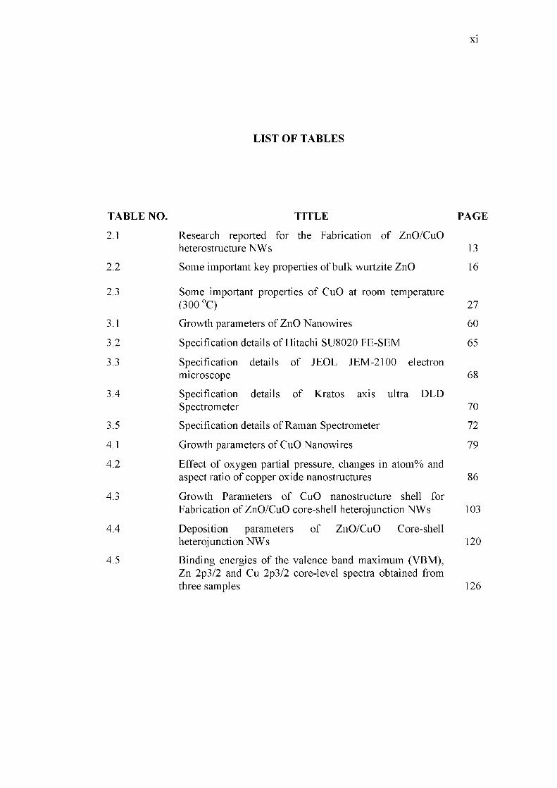
LIST OF TABLES
TABLE NO. TITLE PAGE
2.1 Research reported for the Fabrication of ZnO/CuO heterostructure NWs 13
2.2 Some important key properties of bulk wurtzite ZnO 16
2.3 Some important properties of CuO at room temperature (300 oC) 27
3.1 Growth parameters of ZnO Nanowires 60
3.2 Specification details of Hitachi SU8020 FE-SEM 65
3.3 Specification details of JEOL JEM-2100 electron microscope 68
3.4 Specification details of Kratos axis ultra DLD Spectrometer 70
3.5 Specification details of Raman Spectrometer 72
4.1 Growth parameters of CuO Nanowires 79
4.2 Effect of oxygen partial pressure, changes in atom% and aspect ratio of copper oxide nanostructures 86
4.3 Growth Parameters of CuO nanostructure shell for Fabrication of ZnO/CuO core-shell heterojunction NWs 103
4.4 Deposition parameters of ZnO/CuO Core-shell heterojunction NWs 120
4.5 Binding energies of the valence band maximum (VBM), Zn 2p3/2 and Cu 2p3/2 core-level spectra obtained from three samples 126
xii
LIST OF FIGURES
FIGURE NO. TITLE
2.1. The hexagonal wurtzite structure of ZnO [reproducedfrom Wikipedia]
2.2 I-V characteristic for different ZnO (nanostructures)/p- GaN LEDs
2.3 Schematic band diagram of intrinsic point defects in ZnO
2.4 PL spectra of ZnO NWs on Si substrates by Thermal CVD
2.5 PL spectra of ZnO NWs on sapphire and Si substrates
2.6 XRD patterns of ZnO nanostructures by thermal evaporation synthesized at different source temperatures:(a) 900 0C, (b) 975 0C, and (c) 1050 0C
2.7 XRD patterns of ZnO NWs by thermal CVD synthesized at temperatures 960 0C
2.8 XPS spectra of ZnO nanostructures (a) Zn 2p 3/2 and 1/2,(b) O1s core levels of ZnO NWs by thermal CVD synthesized at temperatures 800 0C
2.9 Copper oxide (CuO) monoclinic crystal structure
2.10 Oxidation states of CuO, Cu2O and Cu
2.11 Optical transmittance of CuO thin films deposited at various growth temperatures. The inset shows the absorbance spectra as a function of wavelength
2.12 (a) The I-V curve of the CuO nanowire measured by C- AFM (b) The plot of the positive current with V1/4 in log scale, which shows linear property
2.13 XRD spectra of the Cu foil after oxidation in wet air, showing: (1) very thin scale formed at 300 oC; (2) mainly Cu2 O with a small amount of CuO formed at 500 oC; and (3) only CuO formed at 800 oC
2.14 (a) core-level XPS spectrum of Cu2p; (b) core-level XPS of O1s for CuO samples
PAGE
15
18
19
20
21
22
23
24
26
28
29
30
31
31
2.15 (a) Depletion layer of pn-junction (b) Energy band structure of CuO/ZnO heterojunction 33
2.16
2.17
2.18
2.19
2.20
2.21
3.1
3.2
3.3
3.4
3.5
3.6
3.7
3.8
3.9
3.10
3.11
3.12
3.13
3.14
3.15
xiii
The characteristic of a p-n junction 35
Vapor-liquid-solid (VLS) Mechanism of Zinc Oxide Nanowires 37
Au-ZnO phase diagram and its eutectic point 38
Schematic diagram illustrates that the metal oxide nanowires via vapor- solid (VS) growth mechanism 40
Thermal Chemical Vapor Deposition (CVD) System 43
Simplified diagram of the experimental setup for CAFM 48
Research Flow Chart 51
Thermal Chemical Vapor Deposition System (a) Fitting for testing of thermal CVD (b) Actual setup of thermal CVD with gasses system at CS (Nano) IIS & IR UTM 52
CVD Tube Furnace system (a) Furnace (b) Bird View 53
Alumina source (Zn) boat (b) Stainless steel rod (c) Alumina flat boat used to hold the substrate at a desired position 56
Silicon substrate, diamond cutter, ruler and sample holding box 57
Schematic of thermal CVD for synthesis of ZnO Nanowires 59
Schematic set-up of thermal oxidation for synthesis of CuO nanowires 61
High Vacuum Dual Target Sputtering System (Q300T D)for deposition of copper nanofilm 62
Fabrication illustration of ZnO/CuO Core-Shell NW arrays 63
FE-SEM Machine, located at UPMU UTM (Hitachi SU8020) 65
HR-TEM machine located at CSNano Ibnu Sina, UTM (JEM-2100) 67
XPS instrument of Advance X-Ray Photoelectron Spectroscopy Laboratory located at UPMU UTM. (AXIS ULTRA DLD) 69
RAMAN Instrument of Advance Optical Microscope and Nano Raman Photoluminescence Laboratory located at UPMU UTM 71
XRD instrument in Mechanical Engineering Laboratory,UTM 73
Photoluminescence (PL) (Horiba Scientist) Laboratory located in physics Department, Faculty of Science 74
3.16
3.17
3.18
4.1
4.2
4.3
4.4
4.5
4.6
4.7
4.8
4.9
4.10
4.11
4.12
xiv
UV-VIS-NIR Scanning Spectrometer Instrument Located in Physics Department Faculty of Science UTM 75
Conductive AFM measurement system 76
Schematic setup of C-AFM for I-V measurement of ZnO/CuO heterojuncti on NW s 77
FE-SEM images of CuO nanowires thermally oxidized on copper foil substrate at temperature 400 °C for time 1h and partial pressure of oxygen 4.65 torr 81
High magnification FE-SEM images of CuO NWs thermally oxidized at 400 °C for time V h in the presence of pure oxygen of partial pressure 4.65 torr. 81
FE-SEM image & their EDX spectra of (a-b) Cu2O thick layer and (c, d) CuO nanowire. 82
(a) FE-SEM image of individual CuO NW (b - d) EDS taken from the single NW top, middle and bottom respectively (e) EDS taken from the background of CuO thin layer. 83
FE-SEM images of CuO nanowires thermally oxidized on copper foil substrate at temperature 400 °C for time V h and partial pressure of oxygen 6.2 torr. 84
FE-SEM images of CuO nanowires thermally oxidized on copper foil substrate at temperature 500 °C for time V h and partial pressure of oxygen 9.31 torr. 85
EDX spectrums of CuO nanowires thermally oxidized on copper foil substrate at temperature 500 °C for time V h and partial pressure of oxygen 9.31 torr 86
XRD spectrum of Cu foil substrate after the thermal oxidation in the presence of pure oxygen at pressure 4.65 torr and temperature 400 oC for 1h. 88
XRD spectrum of Cu foil substrate after the thermal oxidation in the presence of pure oxygen at pressure 6.2 torr and 400 oC for V h. 88
XRD spectrum of Cu foil substrate after the thermal oxidation in the presence of pure oxygen of partialpressure 9.31 torr and temperature 500 oC for V h. 89
((a) Wide scan XPS spectrum of CuO (b) XPS spectra ofO 1s (c) XPS spectra of Cu 2p. 90
Low and high magnification FESEM images of vertically- align ZnO NW arrays grown on Si substrates (a) FESEMimage of ZnO NWs at 3 pm (b) FESEM image of ZnONWs at 2pm (c) FESEM image of ZnO NWs at 1pm (d)FESEM image of ZnO NWs at 1p.m. The inset is shown an enlarged image of ZnO nanowire 92
4.13
4.14
4.15
4.16
4.17
4.18
4.19
4.20
4.21
4.22
4.23
4.24
4.25
100
xv
XRD OF ZnO NW arrays synthesized by Thermal CVD 93
(a) XPS survey spectra of ZnO NW arrays (b, c) High resolution spectra of O 1s and Zn 2p. 94
(a) A low-magnification TEM image of a ZnO NW (b)HRTEM image of a ZnO NW taken from the circle part of single NW shown in Figure 4.15 (a). (c) SAED pattern of the ZnO nanowire indicating the growth direction is [002](d) EDX analysis of Pure ZnO nanowires 96
Raman spectra of pure ZnO NW arrays. 97
Photoluminescence (PL) and UV-Visible reflectance spectra are at room temperature 98
FE-SEM images of low magnification and high magnification respectively (a) and (b) Pure ZnO NW arrays grown on Si substrates (c) and (d) ZnO/Cu coreshell NW arrays (e) and (f) ZnO/CuO core-shell NW arrays
(a) FE-SEM images of ZnO/CuO core-shell NW arrays at400 nm magnification and (b) EDX image. 101
Growth progress of the shell layer (CuO) for the ZnO/CuO core-shell nanowires and their X-ray differaction structures as a function of sputtering deposition time of copper nanofilm for (a-b) 2 min, (c-d) 3 min and (e-f) 4 min respectively at 400 oC for 1 h at pressure 75 torr and oxygen 40 - 45 sccm flow rate. 102
ZnO/CuO core-shell NW arrays formed after thermal oxidation of ZnO-Cu core-shell NW arrays at 400 oC for 1h (a) Pressure 50 torr and oxygen 25-30 sccm flow rate(b) XRD for (a). (c) Pressure 75 torr and oxygen 40-45sccm flow rate. (d) XRD for (c). 104
XRD spectrum of (a) Pure ZnO NW arrays (b) ZnO/Cu core-shall NW arrays and (c) ZnO/CuO core-shall NW arrays 105
XPS spectra of ZnO/CuO core-shall NW arrays corresponding to (a) Wide scan profile spectrum of ZnO/CuO core-shall NW arrays (b) O 1s spectrum (c) Cu 2p spectrum and (d) Zn 2p spectrum. 107
Raman spectra of pure ZnO and ZnO/CuO core-shall NW arrays
(a) A low-magnification TEM image of a ZnO NW (b)HRTEM image of a ZnO NW taken from the circle part of single NW shown in Figure 4.25(a). (c) SAED pattern of the ZnO nanowire indicating the growth direction is [002](d) HRTEM image of a ZnO/CuO NW. (e) HRTEM image of a ZnO/CuO nanowire heterostructure showing the interface and shell thickness taken at the edge from
108
111

xvi
4.26
4.27
4.28
4.29
4.30
4.31
4.32
4.33
4.34
4.35
rectangle part of (d). (f) SAED pattern of the ZnO/CuO core-shell nanowire.
HRTEM image of a ZnO/CuO core-shell heterojunction NW showing the interface and shell thickness (a-b)HRTEM image taken vertically from the edge of single ZnO/CuO core-shell heterojunction NW at magnification1 nm and 2 nm respectively (c-d) tilt HRTEM image of single ZnO/CuO core-shell heterojunction NW at magnification 1 nm and 2 nm respectively. 112
EDX spectrums of the NWs at different position (a) tip (b) middle and (c) bottom 113
(a) STEM (HAADF) image taken from one single CuO/ZnO heterojunction nanowire. (b) EDX elemental mapping of Cu (c) EDX elemental mapping of Zn (d)EDX elemental mapping of O. 114
EDX elemental mappings of Cu, O and Zn, respectively taken from one single p-CuO/n-ZnO heterojunction nanowire 115
Room temperature PL spectrum measured from (a) ZnO NWs and (b) the fabricated p-CuO/n-ZnO heterojunction nanostructure 117
UV-VIS-NIR light reflection of (a) ZnO NWs (b) ZnO/CuO heterojunction (sputtered 3 min) and (c) ZnO/CuO heterojunction (sputtered 4 min) 119
(a) Schematic of the C-AFM I - V measurement, the inset is the AFM image of core-shell heterojunction nanowires (b)The I-V characteristics of the n-ZnO/ p-CuO heterojunction diode (c) Semi-log I - V characteristics (d) Schematic energy band diagram of the heterojunction n- ZnO/p-CuO at zero voltage bias showing energy difference from core-level 122
(a) and (b) HRTEM images of ZnO/CuO heterojunction NW at low and high magnification focused on the interface region showing the interface and shell thickness(c) XRD result for the as fabricated ZnO/CuO heterojunction (d) SAED pattern of the ZnO/CuO coreshell nanowire 123
XPS core-level (CL) and Valence-band edge (VBE) spectra (a) CL of Zn 2p3/2 for ZnO (b) CL of Cu 2p3/2 for CuO (c) Zn 2p3/2 for ZnO/CuO heterojunction (d) Cu 2p3/2 for ZnO/CuO heterojunction (e) VBE spectra for ZnO (f)VBE spectra for CuO 125
Schematic energy band diagram of type-II band alignment of p-CuO/n-ZnO heterojunction 127
xvii
LIST OF ABBREVIATIONS
Ar
CVD
CuO
C-AFM
CB
CBO
CSNano
CL
Eg
eV
FTM
FE-SEM
HS
HRTEM
I-V
MFC
NWs
NRs
nm
NIR
O2
PVD
PL
PECVD
SAED
Argon
Chemical Vapor Deposition
Copper Oxide
Conductive Atomic Force Microscopy
Conduction band
Conduction band offset
Centre for Sustainable Nanomaterial
Core-Level
Band gap
Electron volt
Film Thickness Monitor
Field Emission Scanning Electron Microscopy
Heterostructure
High-Resolution Transmission Electron Microscopy
Current-voltage
Mass Flow Controller
Nanowires
Nanorods
Nanometers
Near infrared
Oxygen
Physical Vapor Deposition
Photoluminescence
Plasma Enhanced Chemical Vapor Deposition
Selected Area Electron Diffraction
xviii
STEM - Scanning Transmission Electron Microscopy
Si - Silicon
sccm - Standard cubic centimeter per minute
TCVD - Thermal Chemical Vapor Deposition
TEM - Transmission Electron Microscopy
UV - Ultra-Violet
UV-Vis - Ultra-Violet Visible
VB - Valance band
VBM - Valance Band Maximum
VBO - Valance band offset
VLS - Vapor-Liquid-Solid
VS - Vapor-Solid
XRD - X-rays Diffraction
XEDS - Energy Dispersive X-rays Spectroscopy
XPS - X-ray Photo-electron Spectroscopy
ZnO - Zinc Oxide
Zn - Zinc
xix
LIST OF SYMBOLS
T - Absolute Temperature
n - Ideality Factor
kB - Boltzmann constant
Is - Reverse saturation current
q - charge on electron
V - Applied Voltage
m - slope of straight line
O - Work function
xx
APPENDICES
APPENDIX TITLE PAGE
A XRD Analysis JCPDS Data for Cuprite 147
B XRD Analysis JCPDS Data for Copper 149
C XRD Analysis JCPDS Data for Copper Oxide 151
D XRD Analysis JCPDS Data for Zinc Oxide 153
E Detail Research Flow Chart 156
F FESM & XRD 158
G HRTEM & EDX 159
H Fabrication illustration of ZnO/CuO Core-Shellheterojunction NW arrays 162
I List of Publications 163
CHAPTER 1
INTRODUCTION
1.1 Background
In recent years the research on one-dimensional (1D) nanostructures of
different materials for their remarkable performance and properties have been
increasing and has gained much attention for the device fabrication due to their size
and shape dependent properties. This is the unique reason that nanostructures have
exceptional properties as compare to the bulk materials properties. This is due to the
dependence of the physical properties and chemical properties of one-dimensional
nanostructures on size and shape. One-dimensional nanostructures, including
nanowires (NWs) and nanorods (NRs) are the most studied nanomaterials for their
important future application prospects. High aspect ratio, extremely large surface
area as compared to volume ratio, high porosity and direct conduction path of
nanowires and nanorods are the important key factors compared with other
nanostructures materials. These properties of nanostructure would lead to potential
use for advanced applications in photonic and nano-optoelectronics like field
emission devices, nanogenerators, photovoltaics, sensing, storage devices and
efficient energy conversion (Jie et al., 2010; Dhara and Giri, 2013; Sun, 2015).
Semiconductor nanowires has become one of the most active area of research
within the science, engineering and technology (Fan and Lu, 2005; Yi et al., 2005;
2
Zhang et al., 2012; Khan and Sakrani, 2014). Many materials are under focus with
the potential of developing nano-systems and their combine heterostructure. The
optimization of the performance is the main challenge at the moment. The materials
to be discussed are copper oxide (CuO), zinc oxide (ZnO), and their core-shell
heterojunction. To grow the nanowires of these materials and their heterojunction
nanowires both high temperature methods and low temperatures methods are being
extensively used.
Copper oxide (CuO) is an attractive p-type material with semiconducting
property of direct band gap 1.2 eV and good absorption coefficient. Due to the
intrinsic, stable, direct band gap and p-type nature properties make CuO good
candidate for electrical, optical, sensing, catalysts, photovoltaic and optoelectronics
devices (Xu et al., 2004b; Cheng et al., 2008; Jung et al., 2011; Liang et al., 2011;
Wang et al., 2011a; b; Anandan et al., 2012; Chang and Yang, 2012; Filipic and
Cvelbar, 2012; Willander et al., 2012). 1D nanowires / nanorods of CuO synthesized
by various growth techniques such as thermal decomposition of CuC2 O4 precursors
(Raksa et al., 2005), hydrothermal decomposition route (Kim et al., 2014), self-
catalytic growth process (Chen et al., 2003), and so forth. In comparison to various
synthesizing methods, thermal annealing or thermal oxidation of copper foil using
hot tube vacuum thermal evaporation method is a simple, convenient, and the fast
method for synthesis nanostructures. Due to large surface areas CuO NWs are greatly
desirable. In CuO NWs large surface areas need to high absorption of photons for
greater efficiency in photovoltaic devices (Bao et al., 2009; Kargar et al., 2013a; Pal
et al., 2015), which are used for catalysis and gas-sensing (Chang and Yang, 2012).
In addition CuO NWs can be potentially applicable in gas sensing, magnetic storage
media, in nano-devices for catalysis and for field emitter devices (Liang et al., 2011)
Similarly Zinc Oxide (ZnO) is n-type metal oxide semiconductor and is very
popular due to easiness of growing it in the nanostructure form. ZnO material
possesses both semiconducting and piezoelectric properties (Cha et al., 2008; Aziz et
al., 2014). ZnO due to its popular material has different growth morphology, such as
nanowires, nanorods, nanotubes, nanofibers, nanospheres and nano-tetrapods, nano
3
cabbage, nanocombs, nanowalls and nanoprisms (Wang, 2004). These growth
morphologies have been successfully grown by different methods. Most of the
techniques have high temperature and long time required for the reaction. The
growth techniques of ZnO nanostructure include Hydrothermal methods (Azlinda et
al., 2011), vapour-liquid-solid (VLS) technique (Zhang et al., 2012), catalysed metal
Chemical Vapour Deposition (Yi et al., 2005), thermal chemical vapour deposition
(Cha et al., 2008), plasma enhanced CVD (Liu, 2004), oxidation method (Khanlary
et al., 2012), thermal evaporation (Suhaimi et al., 2014) and laser-ablation (Son et
al., 2007).
ZnO nanostructures have many diverse applications in nano-optoelectronics,
sensors, transducers, piezoelectric elements for nano-generators, sunscreens and
biomedical science, since it is a bio-safe material (Wang, 2004; Fan and Lu, 2005;
Schmidt-Mende and MacManus-Driscoll, 2007; Li et al., 2008; Pan and Zhu, 2009;
Ahmad et al., 2011; Zhang et al., 2012; Wei et al., 2012; H. Asif, 2013; Sun et al.,
2014; Zhan et al., 2015). The direct wide band gap of ZnO ~ 3.4 eV is suitable for
optoelectronic applications due to its short wavelength. ZnO naturally exhibits n-
type semiconductor, while polarity due to native defects such as oxygen vacancies
and zinc interstitials. P-type doping of ZnO is still a challenging problem that is
hindering the possibility of a p-n homojunction ZnO devices (Janotti and Van de
Walle, 2009).
Recently the fabrication of heterostructure (HS) nanowires is being deeply
studied in order to accomplishment the important properties of heterojunction of
different materials. Using heterojunction nanowires approach, researchers are able to
modify/improve the selective property of the oxide nanowires. Oxide nanowires are
expected to have improved charge collection efficiency because of the lower interval
and higher contact area between the p-type and n-type materials. ZnO NWs radial
heterostructure (core-shell) have been reported using several organic/and inorganic
materials (Plank et al., 2008; Wang et al., 2010, 2011b; Lin et al., 2012; Dhara et al.,
2013; Chu et al., 2014; Pradel et al., 2016) . Several new approaches have been used
for the synthesis of ZnO nanowires based on the radial heterostructures. The radial

4
heterostructures of ZnO NWs basically consist of core-shell nanowires, which have
ZnO as a core material, while a thin layer consist of a shell as a secondary material.
The thin shell layer as a secondary element has a strong impact on the properties of
the nanowires; however, individual property of the shell layer is not specific. These
HS shows significant improvement on certain properties, mainly photophysical
properties, like absorption, electron-hole pair generation and recombination rates.
Although the HS are superior for modulation of certain properties, control on the
external layer and formation of high quality interface between the external material
and NW are, however, challenging issues.
Consequently, there is a lot of interest in the fabrication of one dimensional
(1D) ZnO/CuO core-shell heterojunction nanowires for optoelectronic and
nanoelectronic devices applications. As these core-shell heterojunction nanowires are
expected to have improved charge collection efficiency because of the lower interval
and higher contact area between the p-type and n-type materials (Cao et al., 2012).
Different techniques have been combined and developed to grow ZnO/CuO core
shell NWs heterojunction including chemical reactions from aqueous solutions (e.g.
electrodeposition, hydrothermal growth), and vapor phase methods (chemical vapor
deposition through vapor-liquid-solid (VLS) or vapor-solid (VS) growth
mechanisms), Lithography and electrospinning processes and template-directed
methods (Mieszawska et al., 2007; Fang et al., 2009; Hochbaum and Yang, 2010;
Cao et al., 2012). In general, to synthesize one dimensional nanoscale
heterostructures or core-shell heterostructure all these methods can be applied very
carefully by manipulating the experimental growth parameters, such as source
materials, pressure, temperatures and deposition time etc.
1.2 Problem Statement
Research shows that ZnO/CuO core-shell nanowire (NW) heterojunction
have been studied in recent years, with emphasize generally on their synthesis and
5
properties which are interesting and potentially useful for developing new
challenging devices due to their high interfacial area, allowing for more electron-hole
formation or recombination (Wang and Lin, 2009; Wang et al., 2011b; Hsueh et al.,
2012; Kargar et al., 2013b; Sun, 2015). The shell formation of copper oxide (CuO) to
vertically aligned ZnO NW arrays has been reported as an especially attractive
platform for opto-electronic applications because of promising p-type semiconductor
having narrow band gap energy (1.2 eV) and strong absorption of the solar spectrum
(Kim et al., 2014).
Different techniques have been developed to grow ZnO/CuO core-shell NWs
heterojunction including chemical reactions from aqueous solutions (e.g.
electrodeposition, hydrothermal growth) and chemical vapor deposition (CVD)
through vapor liquid solid (VLS) or vapor-solid (VS) growth mechanisms (Wang
and Lin, 2009; Liao et al., 2011; Wang et al., 2011b; Wu et al., 2013). However,
these techniques have limitations to develop cost-effective and efficient
nanomaterials at commercial levels. The chemical reaction method in aqueous
solution needs a predeposited seed layer, and the aqueous environment tends to
produce very short nanowires with low crystallinity, which is not suitable for high
performance nano-devices fabrication (Zhan et al., 2015). Similarly, to grow high-
crystallinity core-shell nanowires heterojunction using high-temperature methods on
a Si substrate needed a layer of gold film as a catalyst (Pan et al., 2011). The usage
of metal catalyst tends to make impure the final synthetic products and potentially
impacting the electrical and optical performance.
The limited combined use of core-shell compositions in nanostructured
materials highlights the lack of versatility in current synthetic techniques and
emphasizes the need for new synthetic techniques to address unmet challenges facing
the photovoltaic community. Further examination showed that less study has been
available on CuO absorber layers (shell formation) synthesized by thermal oxidation
of copper nanofilm by a thermal chemical vapor deposition method in a horizontal
quartz glass reactor compared to widely used chemical methods. Therefore, it is of
great importance to explore new approach to improve the properties of CuO shell
6
formation or absorber layer properties under vapor solid (VS) grown mechanism.
This would be helpful to produce good p-n junction with ZnO NW arrays with
controlled morphology. A modified thermal CVD followed by sputtering and thermal
oxidation methods are proposed which will result in quality of the controlled growth
and vertically aligned large-area ZnO/CuO core-shell nanowire (NW)
heterojunction. The corresponding structural, optical, electrical and their band offsets
properties are expected to improve significantly.
1.3 Research Objectives
The objectives of this research are:
i) To synthesize ZnO and CuO nanowires by thermal CVD and thermal
oxidation methods respectively and measures its properties.
ii) To produce ZnO/CuO core-shell heterojunction nanowire arrays using
thermal CVD followed by sputtering and thermal oxidation methods.
iii) To measure current-voltage (I-V) of this nanowire heterojunction.
iv) To measured valance band offset of ZnO/CuO heterojunction by X-ray
photoelectron spectroscopy (XPS).
1.4 Scope of the Study
The scope of this research are devoted to the development of controlled
growth, vertically aligned ZnO, CuO and their core-shell (ZnO/CuO) heterojunction
nanowires (NWs) and investigation of structural, optical, electrical and their valance
band offset measurement properties at ZnO/CuO heterointerface.
7
The research work has been carried out for the selected materials keeping in
view of their technological importance and mainly focus on the growth of ZnO and
ZnO/CuO NWs. To produce vertically aligned ZnO/CuO core-shell heterojunction
nanowires (NWs), several steps are used and each step is need on benefits and boost
on the information bring into being in the previous steps. These are highlighted in the
experimental section. Modified thermal chemical vapor deposition (CVD) assisted
sputtering techniques followed by thermal oxidation method under controlled growth
conditions are employed to prepare ZnO/CuO core-shell heterojunction nanowires on
n-type Si substrate. Different deposition parameters such as; sputtering deposition
time, oxygen partial pressure and oxygen flow rate are applied to investigate the
growth process and surface evolution of ZnO/CuO core-shell heterojunction
nanowires. The morphology and crystal structure of the as-grown ZnO nanowires
and core-shell heterojunction NW arrays were characterized by field emission
scanning electron microscope (FESEM, SU8020, HITACHI), high-resolution
transmission electron microscopy (HRTEM, TECNAI G2 20 S-TWIN, FEI 200kV)
including special feature of STEM and EDX, X-ray diffractometer (XRD) (Bruker
AXS D5005, Cu K a radiation), X-ray photoelectron spectroscopy (XPS, AXIS
ULTRA DLD) and Raman spectrometer (HORIBA).
The optical property of the ZnO NWs and their core-shell heterojunction
NWs has been analyzed for the prepared samples at room temperature by using
Photoluminescence (PL), UV visible Reflectance spectroscopy (UV-Vis-NIR
Spectrometer). The electrical measurements (I-V characteristic) and rectifying
behavior of ZnO/CuO core-shell heterojunction NWs about the junction development
at interface were studied by Conductive Atomic Force Microscopy (CAFM). Also
the energy band alignment of the core-shell heterostructure nanowire i.e valance
band offset (VBO) and conduction band offset (CBO) were found experimentally
from X-ray photoelectron spectroscopy.
8
1.5 Significance of the Study
Semiconductor nanowires are exclusively interesting having deep impact on
nanoscience studies and nanotechnology application. It has been determined that one
dimensional (1-D) materials exhibit remarkable nano-optoelectronic, thermal and
mechanical properties as compared to bulk materials/ two dimensional thin film
semiconductors. This is the unique reason that nanostructures have exceptional
properties as compare to the bulk materials properties. This is due to the dependence
of the physical properties and chemical properties of one-dimensional nanostructures
on size and shape. Among the 1-D nanostructures, 1-D heterostructures with
modulated compositions and interfaces have recently become of particular interest
with respect to potential applications in nanoscale building blocks of future
optoelectronic devices and systems. Consequently, there is a lot of interest in the
fabrication of one dimensional (1D) ZnO/CuO core-shell heterojunction nanowires
for optoelectronic and nanoelectronic devices applications. As these core-shell
heterojunction nanowires are expected to have improved charge collection efficiency
because of the lower interval and higher contact area between the p-type and n-type
materials. The results of this dissertation research will be benefit for understanding in
the properties of ZnO/CuO core-shell heterojuction nanowires to meet the
requirements of using heterostructure nanaowires in developing high performance
opto-electronic devices.
1.6 Organization of Thesis
The complete research work of this dissertation is organized into a five-
chapter. Chapter 1 begins with the introduction, followed by the research
background, the statement of the research problem, research objectives, scope of the
study, and significance of this research and organization of the study.

9
Chapter 2 presents literature survey of ZnO, CuO and their heterostructure
nanowires, growth techniques including vapour transport growth, chemical vapour
deposition, thermal chemical vapour deposition and physical vapour deposition.
Then it’s followed by electrical properties of semiconductor nanowires by
conductive AFM and valance band offset measurement by X-ray photoelectron
spectroscopy for these heterostructure nanowires.
Chapter 3 is focused on the details of the experimental procedures, which
cover sample preparations of ZnO and CuO NWs fabricated by thermal chemical
vapour deposition (CVD) and thermal oxidation techniques respectively, while
ZnO/CuO Core-Shell heterojunction nanowire arrays were fabricated on a silicon
substrate through vapor-solid (VS) mechanism without using any catalyst or seed
layer via thermal CVD followed by sputtering and thermal oxidation. A brief
description of sample characterization is also discussed in chapter 3.
In the next Chapter 4, reports on the results and discussion of the
characterization part of the synthesised nanowires (CuO, ZnO and their ZnO/CuO
core-shell heterojunction NWs) are presented. To grow these nanowires and their
core-shell heterojunction nanowires successfully, various growth parameter were
studied. The growth mechanism were explained, and the structural, electrical, optical
and their energy band offsets properties of ZnO/CuO core-shell heterojunction NWs
were performed
Finally, in chapter 5, conclusions that are evident from the work results are
summarized and accompanied by a short outlook, which may boost additional efforts
in this exciting and promising field.
REFERENCES
Ahmad, M., Pan, C., Iqbal, J., Gan, L., and Zhu, J. (2009) Bulk synthesis route of the
oriented arrays of tip-shape ZnO nanowires and an investigation of their sensing
capabilities. Chemical Physics Letters, 480, 105-109.
Ahmad, M., Pan, C., Yan, W., and Zhu, J. (2010) Effect of Pb-doping on the
morphology, structural and optical properties of ZnO nanowires synthesized via
modified thermal evaporation. Materials Science and Engineering: B, 174, 55
58.
Ahmad, M., Sun, H., and Zhu, J. (2011) Enhanced photoluminescence and field-
emission behavior of vertically well aligned arrays of In-doped ZnO Nanowires.
ACS applied materials & interfaces, 3, 1299-305.
Ahmad, Z. and Sayyad, M.H. (2009) Electrical characteristics of a high rectification
ratio organic Schottky diode based on methyl red. Optoelectronics and
Advanced Materials, Rapid Communications, 3, 509-512.
Aleszkiewicz, M. and Fronc, K. (2007) Mechanical and Electrical Properties of ZnO-
Nanowire/Si-Substrate Junctions Studied by Scanning Probe Microscopy. Acta
Physica Polonica- A, 112, 255-260.
Alvi, N.H., Usman Ali, S.M., Hussain, S., Nur, O., and Willander, M. (2011)
Fabrication and comparative optical characterization of n-ZnO nanostructures
(nanowalls, nanorods, nanoflowers and nanotubes)/p-GaN white-light-emitting
diodes. Scripta Materialia, 64, 697-700.
Amin, G., Hussain, I., Zaman, S., Bano, N., Nur, O., and Willander, M. (2010)
Current-transport studies and trap extraction of hydrothermally grown ZnO
nanotubes using gold Schottky diode. Physica Status Solidi (A) Applications
and Materials Science, 207, 748-752.
Anandan, S., Lee, G.J., and Wu, J.J. (2012) Sonochemical synthesis of CuO
133
nanostructures with different morphology. Ultrasonics Sonochemistry, 19, 682
686.
Ashkarran, A.A., Afshar, S.A.A., Aghigh, S.M., and Kavianipour, M. (2010)
Photocatalytic activity of ZnO nanoparticles prepared by electrical arc discharge
method in water. Polyhedron, 29, 1370-1374.
Ashkenov, N., Mbenkum, B.N., Bundesmann, C., Riede, V., Lorenz, M., Spemann,
D., Kaidashev, E.M., Kasic, A., Schubert, M., and Grundmann, M. (2003)
Infrared dielectric functions and phonon modes of high-quality ZnO films.
Journal o f Applied Physics, 93, 126.
Aziz, N.S.A., Mahmood, M.R., Yasui, K., and Hashim, A.M. (2014) Seed/catalyst-
free vertical growth of high-density electrodeposited zinc oxide nanostructures
on a single-layer graphene. Nanoscale research letters, 9, 1-7.
Azlinda, A., Khusaimi, Z., Abdullah, S., and Bin Mahmood, M.R. (2011)
Characterization of Urea versus HMTA in the Preparation of Zinc Oxide
Nanostructures by Solution-Immersion Method Grown on Gold-Seeded Silicon
Substrate. Advanced Materials Research, 364, 45-49.
Baek, K.K. and Tuller, H.L. (1993) Electronic characterization of ZnO/CuO
heterojunctions. Sensors and Actuators: B. Chemical, 13, 238-240.
Bao, Q., Li, CM ., Liao, L., Yang, H., Wang, W., Ke, C., Song, Q., Bao, H., Yu, T.,
Loh, K.P., and Guo, J. (2009) Electrical transport and photovoltaic effects of
core-shell CuO/C60 nanowire heterostructure. Nanotechnology, 20, 1-8.
Bastard, G., Brum, J. a, and Ferreira, R. (1991) Electronic States in Semiconductor
Heterostructures. Solid State Physics-Advances in Research and Applications,
44, 229-415.
Behrisch, R. (1981). Sputtering by Particle bombardment. Springer, Berlin. ISBN
978-3-540-10521-3
Bu, I.Y.Y. (2013) Novel all solution processed heterojunction using p-type cupric
oxide and n-type zinc oxide nanowires for solar cell applications. Ceramics
International, 39, 8073-8078.
Bushan B. (2007). Springer Handbook o f Nano-technology. 2nd edition, Springer
Berlin Heidelberg; New York.
134
C. K. Ghosh, S. R. Popuri, T. U. Mahesh, K.K.C. (2009) Preparation of
nanocrystalline CuAlO2 through sol-gel route. J Sol-Gel Sci Technol, 52, 75
81.
Cao, Y., Wu, Z., and Ni, J. (2012) Type-II Core / Shell Nanowire Heterostructures
and Their Photovoltaic Applications. Nano-Micro Letters, 4, 135-141.
Cha, S.N., Song, B.G., Jang, J.E., Jung, J.E., Han, I T., Ha, J.H., Hong, J.P., Kang,
D.J., and Kim, J.M. (2008) Controlled growth of vertically aligned ZnO
nanowires with different crystal orientation of the ZnO seed layer.
Nanotechnology, 19, 235601.
Chambers, S.A., Droubay, T., Kaspar, T.C., Gutowski, M., Chambers, S.A.,
Droubay, T., Kaspar, T.C., and Gutowski, M. (2004) Experimental
determination of valence band maxima for SrTiO3 , TiO2 , and SrO and the
associated valence band offsets with Si ( 001 ). J. Vac. Sci. Technol. B, 22,
2205-2015.
Chang, S. and Yang, T. (2012) Sensing Performance of EGFET pH Sensors with
CuO Nanowires Fabricated on Glass Substrate. International Journal o f
Electrochemical Science, 7, 5020-5027.
Chen, D., Shen, G., Tang, K., and Qian, Y. (2003) Large-scale synthesis of CuO
shuttle-like crystals via a convenient hydrothermal decomposition route.
Journal o f Crystal Growth, 254, 225-228.
Chen, J.T., Zhang, F., Wang, J., Zhang, G. a., Miao, B.B., Fan, X.Y., Yan, D., and
Yan, P.X. (2008) CuO nanowires synthesized by thermal oxidation route.
Journal o f Alloys and Compounds, 454, 268-273.
Chen, Y., Jia, Q., Shen, Z., Zhao, J., Zhao, Z., Ji, H., and Technology, M. (2016) A
CuO-ZnO Nanostructured p-n Junction Sensor for Enhanced n-butanol
Detection. RSC Adv, 6, 2504-2511.
Chen, Y.S., Liao, C.H., Chueh, Y.L., Lai, C.C., Chen, L.Y., Chu, A.K., Kuo, C.T.,
and Wang, H.C. (2014) High performance Cu2O/ZnO core-shell nanorod arrays
synthesized using a nanoimprint GaN template by the hydrothermal growth
technique. Optical Materials Express, 4, 1473-1486.
Cheng, G., Wang, S., Cheng, K., Jiang, X., Wang, L., Li, L., Du, Z., and Zou, G.
(2008) The current image of a single CuO nanowire studied by conductive
135
atomic force microscopy. Applied Physics Letters, 92, 90-93.
Cheng, K., Li, Q., Meng, J., Han, X., Wu, Y., Wang, S., Qian, L., and Du, Z. (2013)
Interface engineering for efficient charge collection in Cu2 O/ZnO
heterojunction solar cells with ordered ZnO cavity-like nanopatterns. Solar
Energy Materials and Solar Cells, 116, 120-125.
Chiu, H.M., Chang, Y.T., Wu, W.W., and Wu, J.M. (2014) Synthesis and
characterization of one-dimensional Ag-doped ZnO/Ga-doped ZnO coaxial
nanostructure diodes. ACS Applied Materials and Interfaces, 6, 5183-5191.
Cho, S. (2013) Optical and Electrical Properties of CuO Thin Films Deposited at
Several Growth Temperatures by Reactive RF Magnetron Sputtering. Met.
Mater. Int, 19, 1327-1331.
Chu, L., Li, L., Ahmad, W., Wang, Z., Xie, X., Rao, J., Liu, N., Su, J., and Gao, Y.
(2014) Bandgap-graded ZnO/(CdS)1- x (ZnS)x coaxial nanowire arrays for
semiconductor-sensitized solar cells. Materials Research Express, 1, 1 -12.
Coleman, V.A. and Jagadish, C. (2006). Basic Properties and Applications of ZnO.
In: Chennupati Jagadish, Stephen J. Pearton. Zinc Oxide Bulk, Thin Films and
Nanostructures: Processing, Properties, and Applications (pp. 1 - 20). Oxford,
UK: Elsevier.
Dalal, S.H., Baptista, D.L., Teo, K.B.K., Lacerda, R.G., Jefferson, D. a, and Milne,
W.I. (2006) Controllable growth of vertically aligned zinc oxide nanowires
using vapour deposition. Nanotechnology, 17, 4811.
Dhara, S. and Giri, P.K. (2013) ZnO Nanowire Heterostructures: Intriguing
Photophysics and Emerging Applications. Reviews in Nanoscience and
Nanotechnology, 2, 147-170.
Dhara, S., Imakita, K., Giri, P.K., Mizuhata, M., and Fujii, M. (2013) Aluminum
doped core-shell ZnO/ZnS nanowires: Doping and shell layer induced
modification on structural and photoluminescence properties. Journal o f
Applied Physics, 114.
Donatini, F., Levy, F., Dussaigne, A., Ferret, P., and Pernot, J. (2014) Direct Imaging
of p - n Junction in Core - Shell GaN Wires. NANO LETTERS, 14, 3491-3498.
Etgar, L., Yanover, D., Capek, R.K., Vaxenburg, R., Xue, Z., Liu, B., Nazeeruddin,
136
M.K., Lifshitz, E., and Gratzel, M. (2013) Core/shell PbSe/PbS QDs TiO2
heterojunction solar cell. Advanced Functional Materials, 23, 2736-2741.
F. M. CAPECE, V. DI CASTRO, C.F. and G.M. (1982) “Copper Chrcmite”
Catalysts: XPS Structure and Correlation with Catalytic Activity. Journal o f
Electron Spectroscopy and Related Phenomena, 27, 119-128.
F. OZYURT KU§, T. SERiN, N.S. (2009) Current transport mechanisms of n-ZnO /
p-CuO heterojunctions. 11, 1855-1859.
Fan, Z. and Lu, J.G. (2005) Zinc oxide nanostructures: synthesis and properties.
Journal o f nanoscience and nanotechnology, 5, 1561-73.
Fang, X., Bando, Y., Gautam, U.K., Zhai, T., Gradecak, S., and Golberg, D. (2009)
Heterostructures and superlattices in one-dimensional nanoscale
semiconductors. Journal o f Materials Chemistry, 19, 5683.
Filipic, G. and Cvelbar, U. (2012) Copper oxide nanowires: a review of growth.
Nanotechnology, 23, 194001.
Fumagalli L., Casuso I., Ferrari G. and Gomila G. (2008). Probing electrical
transport properties at the nanoscale by current-sensing atomic force
microscopy. Applied Scanning Probe Methods. Vol VIII. Springer-Verlag:
Heidelberg. p 421 - 450.
G. Shen, D.Chen, Y.Bando, and D.G. (2008) One-Dimensional Nanoscale
Heterostructures. J. Mater. Sci. Technol., 24, 541-549.
Gacem K., Hdiy A. E, Troyon M., Berbezier I. and Rhonda A. (2010). Conductive
AFM microscopy study of the carrier transport and storage in Ge nanocrystal
grown by dewetting. Nanotechnology, 21, 065706, 1 - 6.
Guangtian Zou (2008). The current image of a single CuO NW studied by
conductive atomic force microscopy. Applied Physics Letter, 92, 223116.
Gao, P., Wang, L., Wang, Y., Chen, Y., Wang, X., and Zhang, G. (2012) One-pot
hydrothermal synthesis of heterostructured ZnO/ZnS nanorod arrays with high
ethanol-sensing properties. Chemistry - A European Journal, 18, 4681-4686.
Gu G., Burghard M., Kim G. T, Dusberg G. S, Chiu P. W., Krstic V., Roth S.and
Han W. Q. (2001). Growth and electrical transport of germanium NWs. Journal
o f Applied Physics, 90, 5747-5751
137
Guo, Z., Zhao, D., Liu, Y., Shen, D., Zhang, J., and Li, B. (2008) Visible and
ultraviolet light alternative photodetector based on ZnO nanowire/n-Si
heterojunction. Applied Physics Letters, 93, 163501.
Guozhong Cao (2005). Nanostructures & nanomaterials-synthesis, properties &
applications. 2nd edition. USA: Imperial College Press. World scientific
publishing. p 67 - 69
H. Asif, M. (2013) Electrochemical Biosensors Based on ZnO Nanostructures to
Measure Intracellular Metal Ions and Glucose. Journal o f Analytical &
Bioanalytical Techniques, 7, 1-9
He, J.H. and Ho, C.H. (2007) The study of electrical characteristics of heterojunction
based on ZnO nanowires using ultrahigh-vacuum conducting atomic force
microscopy. Applied Physics Letters, 91, 233105,1-3.
Ho, S.-T., Wang, C.-Y., Liu, H.-L., and Lin, H.-N. (2008) Catalyst-free selective-
area growth of vertically aligned zinc oxide nanowires. Chemical Physics
Letters, 463, 141-144.
Hochbaum, A.I. and Yang, P. (2010) Semiconductor nanowires for energy
conversion. Chemical reviews, 110, 527-46.
Hsueh, H.T., Chang, S.J., Weng, W.Y., Hsu, C.L., and Hsueh, T.J. (2012)
Fabrication and Characterization of Coaxial p- Fabrication and Characterization
of Coaxial p-Copper Oxide / n-ZnO Nanowire Photodiodes. IEEE Transactions
on Nanotechnology, 11, 127-133.
Hsueh, T., Hsu, C., Chang, S., and Guo, P. (2007) Cu2O / n-ZnO nanowire solar cells
on ZnO : Ga / glass templates. Scripta MATERILIA, 57, 53-56.
Hullavarad, S., Hullavarad, N., Look, D., and Claflin, B. (2009) Persistent
photoconductivity studies in nanostructured ZnO UV sensors. Nanoscale
Research Letters, 4, 1421-1427.
Hussain, M., Ibupoto, Z.H., Abbassi, M.A., Khan, A., Pozina, G., Nur, O., and
Willander, M. (2014) Synthesis of CuO/ZnO Composite Nanostructures, Their
Optical Characterization and Valence Band Offset Determination by X-Ray
Photoelectron Spectroscopy. Journal o f Nanoelectronics and Optoelectronics,
9, 348-356.
138
Hussain, S., Cao, C., Nabi, G., Khan, W.S., Usman, Z., and Mahmood, T. (2011)
Effect of electrodeposition and annealing of ZnO on optical and photovoltaic
properties of the p-Cu2O/n-ZnO solar cells. Electrochimica Acta, 56, 8342
8346.
Igor Beinik. Electrical Characterization o f Semiconductor Nanostructures by
Conductive Probe Based Atomic Force Microscopy Techniques. Ph.D. Thesis.
Montanuniversitat Leoben; 2011
Janotti, A. and Van de Walle, C.G. (2009) Fundamentals of zinc oxide as a
semiconductor. Reports on Progress in Physics, 72, 126501,1-29.
Jiang, X., Herricks, T., and Xia, Y. (2002) CuO Nanowires Can Be Synthesized by
Heating Copper Substrates in Air. Nano Letters, 2, 1333-1338.
Jie, J., Zhang, W., Bello, I., Lee, C.S., and Lee, S.T. (2010) One-dimensional II-VI
nanostructures: Synthesis, properties and optoelectronic applications. Nano
Today, 5, 313-336.
Jung, S., Jeon, S., and Yong, K. (2011) Fabrication and characterization of flower
like CuO-ZnO heterostructure nanowire arrays by photochemical deposition.
Nanotechnology, 22, 015606,1-9.
Kargar, A., Jing, Y., Kim, S.J., Riley, C.T., Pan, X., and Wang, D. (2013) ZnO/CuO
heterojunction branched nanowires for photoelectrochemical hydrogen
generation. ACS Nano, 7, 11112-11120.
Kamran ul Hasan. Graphene and ZnO Nanostructures fo r Nano- Optoelectronic &
Biosensing Applications. Ph.D. Thesis. Linkopings University Sweden; 2012.
Khan, M.A. and Sakrani, S. (2014) Synthesis of Cu2O and ZnO Nanowires and their
Heterojunction Nanowires by Thermal Evaporation: A Short Review. Jurnal
Teknologi, 5, 83-88.
Khanlary, M.R., Vahedi, V., and Reyhani, A. (2012) Synthesis and characterization
of ZnO nanowires by thermal oxidation of zn thin films at various temperatures.
Molecules, 17, 5021-5029.
Kim, S., Lee, Y., Gu, A., You, C., Oh, K., Lee, S., and Im, Y. (2014) Synthesis of
vertically conformal ZnO/CuO core-shell nanowire arrays by electrophoresis-
assisted electroless deposition. Journal o f Physical Chemistry C, 118, 7377-
139
7385.
Ko, K.Y., Kang, H., Park, J., Min, B.W., Lee, H.S., Im, S., Kang, J.Y., Myoung,
J.M., Jung, J.H., Kim, S.H., and Kim, H. (2014) ZnO homojunction core-shell
nanorods ultraviolet photo-detecting diodes prepared by atomic layer
deposition. Sensors and Actuators, A: Physical, 210, 197-204.
Kong X. Y. and Wang Z. L., (2003). Spontaneous Polarization-Induced Nanohelixes,
Nanosprings, and Nanorings of Piezoelectric Nanobelts. Nano Lett., 3, 1625
1631.
Kouklin N., (2008). Cu-Doped ZnO Nanowires for Efficient and Multospectral
Photodetection Applications. Adv. Matter, 20, 2190-2194.
Kraut, E.A., Grant, R.W., Waldrop, J.R., and Kowalczyk, S.P. (1980) Precise
determination of the valence-band edge in X-Ray photoemission spectra:
Application to measurement of semiconductor interface potentials. Physical
Review Letters, 44, 1620-1623.
Kraut, E.A., Grant, R.W., Waldrop, J.R., and Kowalczyk, S.P. (1983) Semiconductor
core-level to valence-band maximum binding-energy differences: Precise
determination by x-ray photoelectron spectroscopy. Physical Review B , 28,
1965-1977.
Kuo T. J., Lin C. N., Kuo C. L., and Huang M. H. (2007). Growth of Ultralong ZnO
Nanowires on Silicon Substrates by Vapor Transport and Their Use as
Recyclable Photocatalysts. Chemistry Materials, 19, 5143-5147
Lai, F., Lin, S., Chen, Z., Hu, H., and Lin, L. (2013) Wrinkling and Growth
Mechanism of CuO Nanowires in Thermal Oxidation of Copper Foil. Chinese
Journal o f Chemical Physics, 26, 585
Law, M., Greene, L.E., Johnson, J.C., Saykally, R., and Yang, P.D. (2005) Nanowire
dye-sensitized solar cells. Nature Materials, 4, 455-459.
Li, H., Huang, Y., Zhang, Q., Qiao, Y., Gu, Y., Liu, J., and Zhang, Y. (2011) Facile
synthesis of highly uniform Mn/Co-codoped ZnO nanowires: optical, electrical,
and magnetic properties. Nanoscale, 3, 654-60.
Li, J., Fang, G.J., Li, C., Yuan, L.Y., Ai, L., Liu, N.S., Zhao, D.S., Ding, K., Li,
G.H., and Zhao, X.Z. (2008) Synthesis and photoluminescence, field emission
140
properties of stalactite-like ZnS-ZnO composite nanostructures. Applied Physics
A: Materials Science and Processing, 90, 759-763.
Liang, J., Kishi, N., Soga, T., and Jimbo, T. (2011) The Synthesis of Highly Aligned
Cupric Oxide Nanowires by Heating Copper Foil. Journal o f Nanomaterials,
2011, 1-8.
Liao, K., Shimpi, P., and Gao, P.-X. (2011) Thermal oxidation of Cu nanofilm on
three-dimensional ZnO nanorod arrays. Journal o f Materials Chemistry, 21,
9564.
Lin, Y., Chen, W.-J., Lu, J., Chang, Y., Liang, C.-T., Chen, Y., and Lu, J.-Y. (2012)
Growth and characterization of ZnO/ZnTe core/shell nanowire arrays on
transparent conducting oxide glass substrates. Nanoscale Research Letters, 7,
401,1-5.
Liu, X., Wu, X., Cao, H., and Chang, R.P.H. (2004) Growth mechanism and
properties of ZnO nanorods synthesized by plasma-enhanced chemical vapor
deposition. Journal o f Applied Physics, 95, 3141-3147.
Liu, X., Du, H., Wang, P., Lim, T.-T., and Sun, X.W. (2014) A high-performance
UV/visible photodetector of Cu2 O/ZnO hybrid nanofilms on SWNT-based
flexible conducting substrates. J. Mater. Chem. C, 2, 9536-9542.
Lopez-Romero, S. and Garcia-H, M. (2013) Photoluminescence and Structural
Properties of ZnO Nanorods Growth by Assisted-Hydrothermal Method. World
Journal o f Condensed Matter Physics, 3, 152-157.
Mahmood, K., Park, S. Bin, and Sung, H.J. (2013) Enhanced photoluminescence,
Raman spectra and field-emission behavior of indium-doped ZnO
nanostructures. Journal o f Materials Chemistry C, 1, 3138.
Maiti, U.N., Maiti, S., Goswami, S., Sarkar, D., and Chattopadhyay, K.K. (2011)
Room temperature deposition of ultra sharp ZnO nanospike arrays on metallic,
non-metallic and flexible carbon fabrics: Efficient field emitters.
CrystEngComm, 13, 1976.
Manjon, F.J., Mari, B., Serrano, J., and Romero, A.H. (2005) Silent Raman modes in
zinc oxide and related nitrides. Journal o f Applied Physics, 97, 1-4.
Mema, R., Yuan, L., Du, Q., Wang, Y., and Zhou, G. (2011) Effect of surface
141
stresses on CuO nanowire growth in the thermal oxidation of copper. Chemical
Physics Letters, 512, 87-91.
Michelle J.S. Spencer. (2012) Gas sensing applications of 1D-nanostructured zinc
oxide: Insights from density functional theory calculations. Progress in
Materials Science, 57, 6425.
Mieszawska, A.J., Jalilian, R., Sumanasekera, G.U., and Zamborini, F.P. (2007) The
synthesis and fabrication of one-dimensional nanoscale heterojunctions. Small,
3, 722-756.
Milton Ohring (2001). Materials Science o f Thin Films, Deposition and Structure.
2nd Edition. Academic Press: USA
Modeshia, D.R., Dunnill, C.W., Suzuki, Y., Al-Ghamdi, A. a., El-Mossalamy, E.H.,
Obaid, A.Y., Basahel, S.N., Alyoubi, A.O., and Parkin, I.P. (2012) Control of
ZnO Nanostructures via Vapor Transport. Chemical Vapor Deposition, 18, 282
288.
Muhammad H. Asif, F.E. and M.W. (2011) Electrochemical Biosensors Based on
ZnO Nanostructures to Measure Intracellular Metal Ions and Glucose. Journal
o f Analytical & Bioanalytical Techniques, 7, 1-9.
Nasibulin, A., Richard, O., Kauppinen, E., Brown, D., Jokiniemi, J., and Altman, I.
(2002) Nanoparticle Synthesis by Copper (II) Acetylacetonate Vapor
Decomposition in the Presence of Oxygen. Aerosol Science and Technology, 36,
899-911.
Niebelschutz M., Cimalla V., Ambacher O., Machleidt T., Ristic J., Calleja E. (2007)
Electrical performance of gallium nitride nanocolumns. Physica E, 37, 200-203
Pal, S., Maiti, S., Maiti, U.N., and Chattopadhyay, K.K. (2015) Low temperature
solution processed ZnO/CuO heterojunction photocatalyst for visible light
induced photo-degradation of organic pollutants. CrystEngComm, 17, 1464
1476.
Pan, C. and Zhu, J. (2009) The syntheses, properties and applications of Si, ZnO,
metal, and heterojunction nanowires. Journal o f Materials Chemistry, 19, 869.
Pan, J., Shen, H., Werner, U., Prades, J.D., Hernandez-Ramirez, F., Soldera, F.,
Mucklich, F., and Mathur, S. (2011) Heteroepitaxy of SnO2 nanowire arrays on
142
TiO2 single crystals: Growth patterns and tomographic studies. Journal o f
Physical Chemistry C, 115, 15191-15197.
Pan, J., Ke, C., Zhu, W., Zhang, Z., Tok, S., and Pan, J. (2015) Energy band
alignment of SnO2 / SrTiO3 epitaxial heterojunction studied by X-ray
photoelectron spectroscopy. surface and interface analysis, 47, 824-827.
Pecharsky V. and Zavalij P. (2005). Fundamentals o f Powder Diffraction and
Structural Characterisation o f Materials. 2nd Edition. Springer: New York
Peksu, E. and Karaagac, H. (2015) Synthesis of ZnO Nanowires and Their
Photovoltaic Application: ZnO Nanowires / AgGaSe2 Thin Film Core-Shell
Solar Cell. 2015.
Plank, N.O. V, Snaith, H.J., Ducati, C., Bendall, J.S., Schmidt-Mende, L., and
Welland, M.E. (2008) A simple low temperature synthesis route for ZnO-MgO
core-shell nanowires. Nanotechnology, 19, 465603.
Pradel, K.C., Ding, Y., Wu, W., Bando, Y., Fukata, N., and Wang, Z.L. (2016)
Optoelectronic Properties of Solution Grown ZnO n - p or p - n Core - Shell
Nanowire Arrays. ACS Applied Materials & Interfaces, 8, 4287-4291.
Raksa, P., Kittikunodom, S., Choopun, S., Chairuangsri, T., Mangkorntong, P., and
Mangkorntong, N. (2005) CuO Nanowires by Oxidation Reaction. CMU.
Journal Special Issue on Nanotechnology, 4, 1-5.
Schmidt-Mende, L. and MacManus-Driscoll, J.L. (2007) ZnO - nanostructures,
defects, and devices. Materials Today, 10, 40-48.
Seghier, D. and Gislason, H.P. (2008) Shallow and deep donors in n-type ZnO
characterized by admittance spectroscopy. Journal o f Materials Science:
Materials in Electronics, 19, 687-691.
Shen, G. and Chen, D. (2010) One-dimensional nanostructures for electronic and
optoelectronic devices. Frontiers o f Optoelectronics in China, 3, 125-138.
Shinde, S.K., Dubal, D.P., Ghodake, G.S., and Fulari, V.J. (2014) Hierarchical 3D-
flower-like CuO nanostructure on copper foil for supercapacitors. RSC Adv., 5,
4443-4447.
Son, H.J., Jeon, K.A., Kim, C.E., Kim, J.H., Yoo, K.H., and Lee, S.Y. (2007)
Synthesis of ZnO nanowires by pulsed laser deposition in furnace. Applied
143
Surface Science, 253, 7848-7850.
Sreedharan, R.S., Ganesan, V., Sudarsanakumar, C.P., Bhavsar, K., Prabhu, R., and
Mahadevan Pillai, V.P.P. (2015) Highly textured and transparent RF sputtered
Eu2O3 doped ZnO films. Nano Reviews, 6, 1-16.
Suhaimi, S., Sakrani, S., Dorji, T., and Ismail, A.K. (2014) A catalyst-free growth of
aluminum-doped ZnO nanorods by thermal evaporation. Nanoscale Research
Letters, 9, 256.
Sun, S. (2015) Recent advances in hybrid Cu2O-based heterogeneous nanostructures.
Nanoscale, 7, 10850-10882.
Sun, S., Sun, Y., Chen, A., Zhang, X., and Yang, Z. (2015) Nanoporous copper oxide
ribbon assembly of free-standing nanoneedles as biosensors for glucose. The
Analyst, 140, 5205-5215.
Sun, X., Li, Q., Jiang, J., and Mao, Y. (2014) Morphology-tunable synthesis of ZnO
nanoforest and its photoelectrochemical performance. Nanoscale, 6, 8769-80.
Tian, B., Zheng, X., Kempa, T.J., Fang, Y., Yu, N., Yu, G., Huang, J., and Lieber,
C.M. (2007) Coaxial silicon nanowires as solar cells and nanoelectronic power
sources. Nature, 449, 885-889.
Thomas Martensson. Semiconductor Nanowires: Epitaxy and Applications. Ph.D.
Thesis. Lund University Sweden; 2008
Wang, G., San, X., Bing, L., Song, Y., Gao, S., Zhang, J., and Meng, F. (2015)
Catalyst-free growth of one-dimensional ZnO nanostructures on SiO2 substrate
and in situ investigation of their H2 sensing properties. Journal o f Alloys and
Compounds, 622, 73-78.
Wang, J.X., Sun, X.W., Yang, Y., Kyaw, K.K. a, Huang, X.Y., Yin, J.Z., Wei, J., and
Demir, H. V. (2011) Free-standing ZnO-CuO composite nanowire array films
and their gas sensing properties. Nanotechnology, 22, 325704.
Wang, K., Chen, J.J., Zeng, Z.M., Tarr, J., Zhou, W.L., Zhang, Y., Yan, Y.F., Jiang,
C.S., Pern, J., and Mascarenhas, A. (2010) Synthesis and photovoltaic effect of
vertically aligned ZnO/ZnS core/shell nanowire arrays. Applied Physics Letters,
96, 1-4.
Wang, P., Zhao, X., and Li, B. (2011) ZnO-coated CuO nanowire arrays:
144
fabrications, optoelectronic properties, and photovoltaic applications. Optics
express, 19, 11271-11279.
Wang, R.C. and Lin, H.Y. (2009) ZnO-CuO core-shell nanorods and CuO-
nanoparticle-ZnO-nanorod integrated structures. Applied Physics A: Materials
Science and Processing, 95, 813-818.
Wang, S.B., Hsiao, C.H., Chang, S.J., Jiao, Z.Y., Young, S.J., Hung, S.C., and
Huang, B.R. (2013) ZnO branched nanowires and the p-CuO/n-ZnO
heterojunction nanostructured photodetector. IEEE Transactions on
Nanotechnology, 12, 263-269.
Wang, Z., Jia, C., Chen, Y., Guo, Y., Liu, X., Yang, S., Zhang, W., and Wang, Z.
(2011) Valence band offset of InN / BaTiO3 heterojunction measured by X-ray
photoelectron spectroscopy. Nanoscale Research Letters, 6, 1-5.
Wang, Z.L. (2004) Zinc oxide nanostructures: growth, properties and applications.
Journal o f Physics: Condensed Matter, 16, R829-R858.
Wei, A., Xiong, L., Sun, L., Liu, Y.-J., and Li, W.-W. (2013) CuO Nanoparticle
Modified ZnO Nanorods with Improved Photocatalytic Activity. Chinese
Physics Letters, 30, 46202.
Wei, H., Gong, H., Wang, Y., Hu, X., Chen, L., Xu, H., Liu, P., and Cao, B. (2011)
Three kinds of Cu2 O/ZnO heterostructure solar cells fabricated with
electrochemical deposition and their structure-related photovoltaic properties.
CrystEngComm, 13, 6065.
Wei, Y., Ke, L., Kong, J., Liu, H., Jiao, Z., Lu, X., Du, H., and Sun, X.W. (2012)
Enhanced photoelectrochemical water-splitting effect with a bent ZnO nanorod
photoanode decorated with Ag nanoparticles. Nanotechnology, 23, 235401.
Willander, M., Yang, L.L., Wadeasa, a., Ali, S.U., Asif, M.H., Zhao, Q.X., and Nur,
O. (2009) Zinc oxide nanowires: controlled low temperature growth and some
electrochemical and optical nano-devices. Journal o f Materials Chemistry, 19,
1006.
Willander, M., ul Hasan, K., Nur, O., Zainelabdin, A., Zaman, S., and Amin, G.
(2012) Recent progress on growth and device development of ZnO and CuO
nanostructures and graphene nanosheets. Journal o f Materials Chemistry, 22,
2337.
145
Wilson, S.S., Tolstova, Y., Scanlon, D.O., Watson, G.W., and Atwater, H.A. (2014)
Interface stoichiometry control to improve device voltage and modify band
alignment in ZnO / Cu2 O heterojunction solar cells. Energy & Environmental
Science, 7, 3606-3610.
Wu, J.-K., Chen, W.-J., Chang, Y.H., Chen, Y.F., Hang, D.-R., Liang, C.-T., and Lu,
J.-Y. (2013) Fabrication and photoresponse of ZnO nanowires/CuO coaxial
heterojunction. Nanoscale research letters, 8, 387.
Xu, C.H., Woo, C.H., and Shi, S.Q. (2004a) Formation of CuO nanowires on Cu foil.
Chemical Physics Letters, 399, 62-66.
Xu, C.H., Woo, C.H., and Shi, S.Q. (2004b) The effects of oxidative environments
on the synthesis of CuO nanowires on Cu substrates. Superlattices and
Microstructures, 36, 31-38.
Xu, J.F., Ji, W., Shen, Z.X., Li, W.S., Tang, S.H., Ye, X.R., Jia, D.Z., and Xin, X.Q.
(1999) Raman spectra of CuO nanocrystals. Journal o f Raman Spectroscopy,
30, 413-415.
Xu, S. and Wang, Z.L. (2011) One-dimensional ZnO nanostructures: Solution
growth and functional properties. Nano Research, 4, 1013-1098.
Yang, Z., Zhu, L., Guo, Y., Tian, W., Ye, Z., and Zhao, B. (2011) Valence-band
offset of p-NiO / n-ZnO heterojunction measured by X-ray photoelectron
spectroscopy. Physics Letters A, 375, 1760-1763.
Yi, G.-C., Wang, C., and Park, W. Il. (2005) ZnO nanorods: synthesis,
characterization and applications. Semiconductor Science and Technology, 20,
S22-S34.
Yu, B. and Meyyappan, M. (2006) Nanotechnology: Role in emerging
nanoelectronics. Solid-State Electronics, 50, 536-544.
Yuan, Z., Yu, J., Ma, W., and Jiang, Y. (2012) A photodiode with high rectification
ratio based on well-aligned ZnO nanowire arrays and regioregular poly(3-
hexylthiophene-2,5-diyl) hybrid heterojunction. Applied Physics A: Materials
Science and Processing, 106, 511-515.
Zainelabdin, A., Zaman, S., Amin, G., Nur, O., and Willander, M. (2012) Optical and
current transport properties of CuO/ZnO nanocoral p-n heterostructure
146
hydrothermally synthesized at low temperature. Applied Physics A: Materials
Science and Processing, 108, 921-928.
Zeng, H., Xu, X., Bando, Y., Gautam, U.K., Zhai, T., Fang, X., Liu, B., and Golberg,
D. (2009) Template deformation-tailored ZnO nanorod/nanowire arrays: Full
growth control and optimization of field-emission. Advanced Functional
Materials, 19, 3165-3172.
Zhan, Z., Xu, L., Li, X., Wang, L., Feng, S., Chai, X., Lu, W., Shen, J., Weng, Z.,
and Sun, J. (2015) Catalyst-Free, Selective Growth of ZnO Nanowires on SiO2
by Chemical Vapor Deposition for Transfer-Free Fabrication of UV
Photodetectors. ACS Applied Materials & Interfaces, 7, 20264-20271.
Zhang, Y., Ram, M.K., Stefanakos, E.K., and Goswami, D.Y. (2012) Synthesis,
characterization, and applications of ZnO nanowires. Journal o f Nanomaterials,
2012, 1-22.
Zhao, R., Zhu, L., Cai, F., Yang, Z., Gu, X., Huang, J., and Cao, L. (2013) ZnO/TiO2
core-shell nanowire arrays for enhanced dye-sensitized solar cell efficiency.
Applied Physics A: Materials Science and Processing, 113, 67-73.
Zhu, H., Iqbal, J., Xu, H., and Yu, D. (2008) Raman and photoluminescence
properties of highly Cu doped ZnO nanowires fabricated by vapor-liquid-solid
process. Journal o f Chemical Physics, 129, 1-5.