SX48BD/SX52BD - Digi-Key Sheets/Parallax PDFs/SX48BD_SX52BD.pdfSX48BD/SX52BD Configurable...
58
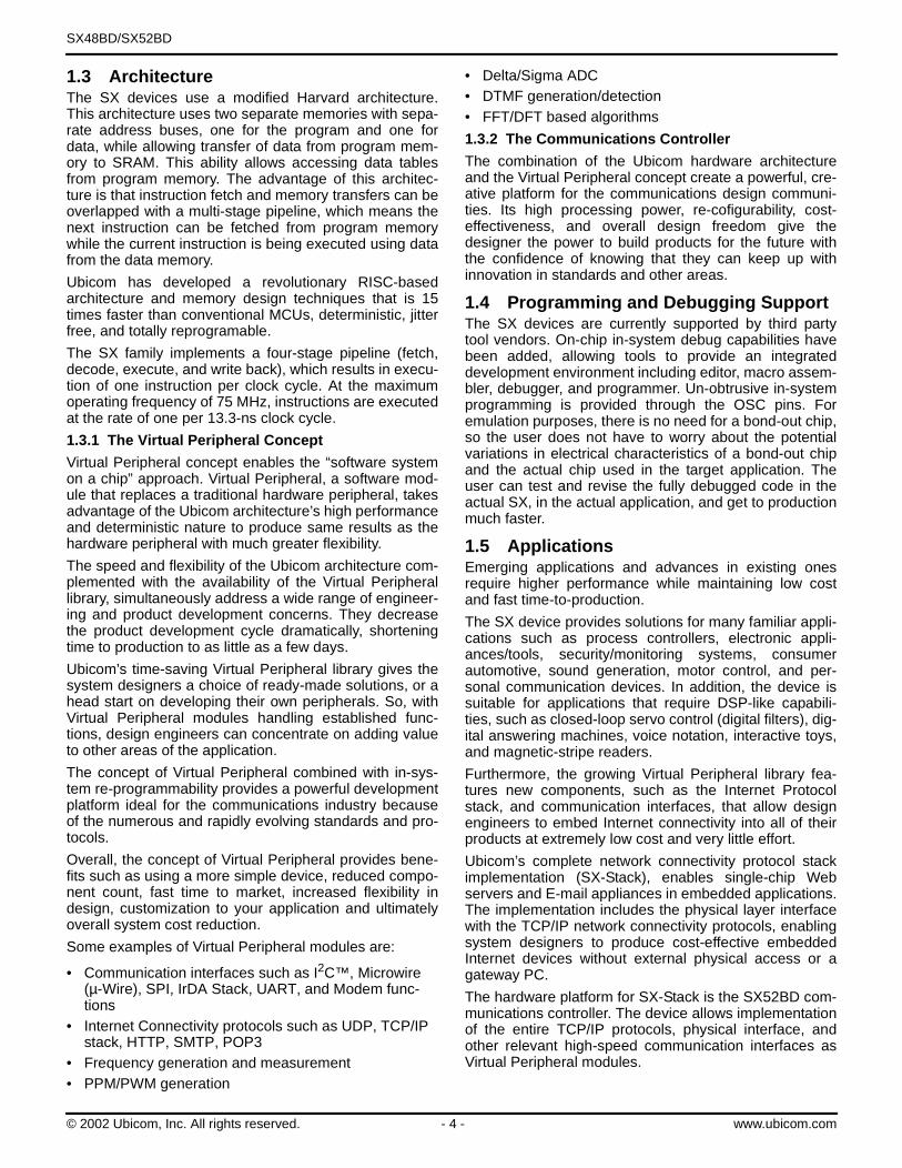
© 2002 Ubicom, Inc. All rights reserved. - 1 - www.ubicom.com Ubicom™ and the Ubicom logo are trademarks of Ubicom, Inc. I 2 C™ is a trademark of Philips Corporation. All other trademarks mentioned in this document are property of their respec- tive companies. April, 2002 SX48BD/SX52BD Configurable Communications Controllers with EE/Flash Program Memory, In-System Programming Capability, and On-Chip Debug 1.0 PRODUCT OVERVIEW 1.1 Introduction The Ubicom SX48BD/SX52BD are members of the SX family of configurable communications controllers fabri- cated in an advanced CMOS process technology. The advanced process, combined with a RISC-based archi- tecture, allows high-speed computation, flexible I/O con- trol, and efficient data manipulation. Throughput is enhanced by operating the device at frequencies up to 75 MHz and by optimizing the instruction set to include mostly single-cycle instructions. In addition, the SX archi- tecture is deterministic and totally reprogramable. The unique combination of these characteristics enables the device to implement hard real-time functions as software modules (Virtual Peripheral™) to replace traditional hard- ware functions. On-chip functions include two 16-bit timers with 8-bit prescalers supporting different operating modes (PWM, simultaneous PWM/capture, and external event counter), a general-purpose 8-bit timer with prescaler, an analog comparator, a brown-out detector, a watchdog timer, a power-save mode with multi-source wakeup capability, an internal R/C oscillator, user-selectable clock modes, and high-current outputs. The SX48BD and SX52BD are functionally the same, except for the package type and pinout. The SX48BD has four fewer pins and has only four rather than eight I/O pins for Port A. Figure 1-1. Block Diagram Interrupt MIWU Port B COMPARATOR Power-On Reset RESET 8-bit Watchdog Timer (WDT) 8-bit Timer RTCC 8 Internal Data Bus System Clock Brown-Out MIWU MCLR OSC Driver 4MHz Internal RC OSC (divided by Clock Select System Clock OSC1 OSC2 8 3 8 steps) 8-Bit Prescaler 16-Bit Timer 2 Port A 4/8 Port C Port D Port E 8 8 8 8 8 8 8 8 In-System Debugging In-System Programming 4k Words EEPROM 262 Bytes SRAM Address Write Data Read Data Instruction W FSR STATUS PC MODE OPTION Fetch 8 8 12 Address 12 8 8 8 8 ALU 8 8 8 PC 8 Level Decode Execute Write Back IREAD Stack Instruction Pipeline Interrupt Stack Prescaler for RTCC Postscaler for WDT or Data 8-Bit Prescaler 16-Bit Timer 1 Port B Port C RTCC WDT Clock SLEEP Clock
Transcript of SX48BD/SX52BD - Digi-Key Sheets/Parallax PDFs/SX48BD_SX52BD.pdfSX48BD/SX52BD Configurable...

© 2002 Ubicom, Inc. All rights reserved. - 1
Ubicom™ and the Ubicom logo are trademarks of Ubicom, Inc.I2C™ is a trademark of Philips Corporation.
April, 2002
SX48BD/SX52BDConfigurable Communications Controllers with EE/Flash Program Memory, In-System Programming Capability, and On-Chip Debug
1.0 PRODUCT OVERVIEW1.1 IntroductionThe Ubicom SX48BD/SX52BD are members of the SXfamily of configurable communications controllers fabri-cated in an advanced CMOS process technology. Theadvanced process, combined with a RISC-based archi-tecture, allows high-speed computation, flexible I/O con-trol, and efficient data manipulation. Throughput isenhanced by operating the device at frequencies up to 75MHz and by optimizing the instruction set to includemostly single-cycle instructions. In addition, the SX archi-tecture is deterministic and totally reprogramable. Theunique combination of these characteristics enables thedevice to implement hard real-time functions as softwaremodules (Virtual Peripheral™) to replace traditional hard-ware functions.
On-chip functions include two 16-bit timers with 8-bitprescalers supporting different operating modes (PWM,simultaneous PWM/capture, and external event counter),a general-purpose 8-bit timer with prescaler, an analogcomparator, a brown-out detector, a watchdog timer, apower-save mode with multi-source wakeup capability,an internal R/C oscillator, user-selectable clock modes,and high-current outputs.
The SX48BD and SX52BD are functionally the same,except for the package type and pinout. The SX48BDhas four fewer pins and has only four rather than eightI/O pins for Port A.
Interrupt MIWU
Port B COMPARATOR
Power-On
8-bit Watchdog Timer (WDT)
8-bit TimerRTCC
MCLR
OSC Driver
4MHz InternalRC OSC
(divided by
ClockSelect
System Clock
OSC1 OSC2
83
8 steps)
Port A
4/8
Port C Port D Port E
8 8 8
InterruptStack
Prescaler for RTCC
RTCCWDT Clock
SLE
EP
Clo
ck
Figure 1-1. Block Diagram
Reset RESET8
Internal Data Bus
SystemClock
Brown-OutMIWU
8-BitPrescaler
16-BitTimer 2
8 8 8 8 8
In-SystemDebugging
In-SystemProgramming
4k WordsEEPROM
262 BytesSRAM
Address
Write DataRead Data
Instruction
W
FSR
STATUS
PC
MODE
OPTION
Fetch
88
12
Address 12
8
88
8
ALU
88 8PC
8 Level
Decode
Execute
Write Back
IREAD
Stack
InstructionPipeline
Postscaler for WDTor
Data8-Bit
Prescaler
16-BitTimer 1
Port B Port C
- www.ubicom.com
All other trademarks mentioned in this document are property of their respec-tive companies.

SX48BD/SX52BD
Table of Contents1.0 Product Overview . . . . . . . . . . . . . . . . . . . . . . . . . . . . . . . . . . 1
1.1 Introduction . . . . . . . . . . . . . . . . . . . . . . . . . . . . . . . 11.2 Key Features . . . . . . . . . . . . . . . . . . . . . . . . . . . . . . 31.3 Architecture . . . . . . . . . . . . . . . . . . . . . . . . . . . . . . . 4
1.3.1 The Virtual Peripheral Concept . . . . . . . . 41.3.2 The Communications Controller . . . . . . . 4
1.4 Programming and Debugging Support . . . . . . . . . . 41.5 Applications . . . . . . . . . . . . . . . . . . . . . . . . . . . . . . . 4
2.0 Connection Diagrams . . . . . . . . . . . . . . . . . . . . . . . . . . . . . . . 52.1 Pin Assignments . . . . . . . . . . . . . . . . . . . . . . . . . . . 52.2 Pin Descriptions . . . . . . . . . . . . . . . . . . . . . . . . . . . 62.3 Part Numbering . . . . . . . . . . . . . . . . . . . . . . . . . . . . 7
3.0 Port Descriptions . . . . . . . . . . . . . . . . . . . . . . . . . . . . . . . . . . 83.1 Reading and Writing the Ports . . . . . . . . . . . . . . . . . 83.2 Read-Modify-Write Considerations . . . . . . . . . . . . 113.3 Port Configuration . . . . . . . . . . . . . . . . . . . . . . . . . 11
3.3.1 MODE Register . . . . . . . . . . . . . . . . . . . 113.3.2 Port Configuration Registers . . . . . . . . . 133.3.3 Port Configuration Upon Power-Up . . . . 13
4.0 Special-Function Registers . . . . . . . . . . . . . . . . . . . . . . . . . 144.1 PC Register (02h) . . . . . . . . . . . . . . . . . . . . . . . . . 144.2 STATUS Register (03h) . . . . . . . . . . . . . . . . . . . . . 144.3 OPTION Register . . . . . . . . . . . . . . . . . . . . . . . . . . 154.4 DEVICE CONFIGURATION AND ID REGISTERS 154.5 FUSE Word (Read/Program via programming
command) 164.6 FUSEX Word (Read/Program via Programming
Command) 174.7 DEVICE ID Word (Hard-Wired Read-Only Via
Programming Command)- Part ID Code . . . . . . . . 174.8 User Code ID . . . . . . . . . . . . . . . . . . . . . . . . . . . . . 17
5.0 Memory Organization . . . . . . . . . . . . . . . . . . . . . . . . . . . . . . 185.1 Program Memory . . . . . . . . . . . . . . . . . . . . . . . . . . 18
5.1.1 Program Counter . . . . . . . . . . . . . . . . . . 185.1.2 Subroutine Stack . . . . . . . . . . . . . . . . . . 18
5.2 Data Memory . . . . . . . . . . . . . . . . . . . . . . . . . . . . . 185.2.1 Addressing Modes/FSR . . . . . . . . . . . . . 185.2.2 Register Access Examples . . . . . . . . . . 20
6.0 Power Down Mode . . . . . . . . . . . . . . . . . . . . . . . . . . . . . . . . 216.1 Multi-Input Wakeup . . . . . . . . . . . . . . . . . . . . . . . . 216.2 Port B MIWU/Interrupt Configuration . . . . . . . . . . . 22
7.0 Interrupt Support . . . . . . . . . . . . . . . . . . . . . . . . . . . . . . . . . 238.0 Oscillator Circuits . . . . . . . . . . . . . . . . . . . . . . . . . . . . . . . . . 25
8.1 XT, LP or HS modes . . . . . . . . . . . . . . . . . . . . . . . 258.2 External RC Mode . . . . . . . . . . . . . . . . . . . . . . . . . 258.3 Internal RC Mode . . . . . . . . . . . . . . . . . . . . . . . . . . 26
9.0 Real Time Clock/Counter (RTCC)/Watchdog Timer . . . . . . 279.1 RTCC . . . . . . . . . . . . . . . . . . . . . . . . . . . . . . . . . . . 279.2 Watchdog Timer . . . . . . . . . . . . . . . . . . . . . . . . . . . 279.3 The Prescaler . . . . . . . . . . . . . . . . . . . . . . . . . . . . . 27
10.0 Multi-Function Timers . . . . . . . . . . . . . . . . . . . . . . . . . . . . . .2910.1 Timer Registers . . . . . . . . . . . . . . . . . . . . . . . . . . .2910.2 Timer Operating Modes . . . . . . . . . . . . . . . . . . . . .30
10.2.1 PWM Mode . . . . . . . . . . . . . . . . . . . . . .3010.2.2 Software Timer Mode . . . . . . . . . . . . . . .3010.2.3 External Event Mode . . . . . . . . . . . . . . .3010.2.4 Capture/Compare Mode . . . . . . . . . . . . .31
10.3 Timer Pin Assignments . . . . . . . . . . . . . . . . . . . . .3110.4 Timer Control Registers . . . . . . . . . . . . . . . . . . . . .31
11.0 Comparator . . . . . . . . . . . . . . . . . . . . . . . . . . . . . . . . . . . . . .3612.0 Reset . . . . . . . . . . . . . . . . . . . . . . . . . . . . . . . . . . . . . . . . . . . .3813.0 Brown-Out Detector . . . . . . . . . . . . . . . . . . . . . . . . . . . . . . .3914.0 Register States Upon Different Reset Conditions . . . . . . .4015.0 Instruction Set . . . . . . . . . . . . . . . . . . . . . . . . . . . . . . . . . . . .41
15.1 Instruction Set Features . . . . . . . . . . . . . . . . . . . . .4115.2 Instruction Execution . . . . . . . . . . . . . . . . . . . . . . .4115.3 Addressing Modes . . . . . . . . . . . . . . . . . . . . . . . . .4215.4 The Bank Instruction . . . . . . . . . . . . . . . . . . . . . . .4215.5 Bit Manipulation . . . . . . . . . . . . . . . . . . . . . . . . . . .4215.6 Input/Output Operation . . . . . . . . . . . . . . . . . . . . . .42
15.6.1 Read-Modify-Write Considerations . . . .4215.7 Increment/Decrement . . . . . . . . . . . . . . . . . . . . . . .4215.8 Loop Counting and Data Pointing Testing . . . . . . .4215.9 Branch and Loop Call Instructions . . . . . . . . . . . . .43
15.9.1 Jump Operation . . . . . . . . . . . . . . . . . . .4315.9.2 Page Jump Operation . . . . . . . . . . . . . .4315.9.3 Call Operation . . . . . . . . . . . . . . . . . . . .4315.9.4 Page Call Operation . . . . . . . . . . . . . . . .43
15.10 Return Instructions . . . . . . . . . . . . . . . . . . . . . . . . .4315.11 Subroutine Operation . . . . . . . . . . . . . . . . . . . . . . .44
15.11.1 Push Operation . . . . . . . . . . . . . . . . . . .4415.11.2 Pop Operation . . . . . . . . . . . . . . . . . . . .44
15.12 Comparison and Conditional Branch Instructions .4515.13 Logical Instruction . . . . . . . . . . . . . . . . . . . . . . . . .4515.14 Shift and Rotate Instructions . . . . . . . . . . . . . . . . .4515.15 Complement and SWAP . . . . . . . . . . . . . . . . . . . .4515.16 Key to Abbreviations and Symbols . . . . . . . . . . . . .45
16.0 Instruction Set Summary Table . . . . . . . . . . . . . . . . . . . . . .4616.1 Equivalent Assembler Mnemonics . . . . . . . . . . . . .49
17.0 Electrical Characteristics . . . . . . . . . . . . . . . . . . . . . . . . . . .5017.1 Absolute Maximum Ratings (beyond which
permanent damage may occur) 5017.2 DC Characteristics . . . . . . . . . . . . . . . . . . . . . . . . .5117.3 AC Characteristics . . . . . . . . . . . . . . . . . . . . . . . . .5217.4 Comparator DC and AC Specifications . . . . . . . . .5417.7 Typical Performance Characteristics (Room
Temperature) . . . . . . . . . . . . . . . . . . . . . . . . . . . . .5618.0 Package Dimensions . . . . . . . . . . . . . . . . . . . . . . . . . . . . . .57
© 2002 Ubicom, Inc. All rights reserved. - 2 - www.ubicom.com

SX48BD/SX52BD
1.2 Key Features75 MIPS Performance
• DC - 75 MHz operation• 13.3 ns instruction cycle, 39.9 ns internal interrupt re-
sponse at 75 MHz• 1 instruction per clock (branches 3)
EE/FLASH Program Memory ad SRAM Data Memory
• Access time of < 13.3 ns provides single cycle access• EE/Flash rated for > 10,000 rewrite cycles• 4096 Words of EE/Flash program memory• 262x8 bits SRAM data memory
CPU Features
• Compact instruction set• All instructions are single cycle except branch• Eight-level push/pop hardware stack for subroutine
linkage• Fast table lookup capability through run-time readable
code (IREAD instruction)• Predictable program execution flow for hard real-time
applications
Fast and Deterministic Interrupt
• Jitter-free 3-cycle internal interrupt response• Hardware context save/restore of key resources such
as PC, W, STATUS, and FSR within the 3-cycle inter-rupt response time
• External wakeup/interrupt capability on Port B (8 pins)
Flexible I/O
• All pins individually programmable as I/O• Inputs are TTL or CMOS level selectable• All pins have selectable internal pull-ups• Selectable Schmitt Trigger inputs on Ports B, C, D, and
E• All outputs capable of sourcing/sinking 30 mA• Port A outputs have symmetrical drive• Analog comparator support on Port B (RB0 OUT, RB1
IN-, RB2 IN+)• Selectable I/O operation synchronous to the oscillator
clock
Hardware Peripheral Features
• Two 16-bit timers with 8-bit prescalers supporting:– Software Timer mode– PWM mode– Simultaneous PWM/Capture mode– External Event mode
• One 8-bit Real Time Clock/Counter (RTCC) with pro-gramable 8-bit prescaler
• Watchdog Timer (shares the RTCC prescaler)• Analog comparator• Brown-out detector• Multi-Input Wakeup logic on 8 pins• Internal RC oscillator with configurable rate from 31.25
kHz to 4 MHz• Power-On-Reset
Packages
• 48-pin Tiny PQFP, and 52-pin PQFP
Programming and Debugging Support
• On- chip in-system programming support with serial or parallel interface
• In-system serial programming via oscillator pins• On-chip in-System debugging support logic• Real-time emulation, full program debug, and integrat-
ed development environment offered by third party tool vendors
Software Support
• Library of off-the-shelf Virtual Peripheral modules• Examples of Virtual Peripheral integration• Evaluation Kits for communication intensive applica-
tions
© 2002 Ubicom, Inc. All rights reserved. - 3 - www.ubicom.com
SX48BD/SX52BD
1.3 ArchitectureThe SX devices use a modified Harvard architecture.This architecture uses two separate memories with sepa-rate address buses, one for the program and one fordata, while allowing transfer of data from program mem-ory to SRAM. This ability allows accessing data tablesfrom program memory. The advantage of this architec-ture is that instruction fetch and memory transfers can beoverlapped with a multi-stage pipeline, which means thenext instruction can be fetched from program memorywhile the current instruction is being executed using datafrom the data memory.
Ubicom has developed a revolutionary RISC-basedarchitecture and memory design techniques that is 15times faster than conventional MCUs, deterministic, jitterfree, and totally reprogramable.
The SX family implements a four-stage pipeline (fetch,decode, execute, and write back), which results in execu-tion of one instruction per clock cycle. At the maximumoperating frequency of 75 MHz, instructions are executedat the rate of one per 13.3-ns clock cycle.
1.3.1 The Virtual Peripheral Concept
Virtual Peripheral concept enables the “software systemon a chip” approach. Virtual Peripheral, a software mod-ule that replaces a traditional hardware peripheral, takesadvantage of the Ubicom architecture’s high performanceand deterministic nature to produce same results as thehardware peripheral with much greater flexibility.
The speed and flexibility of the Ubicom architecture com-plemented with the availability of the Virtual Peripherallibrary, simultaneously address a wide range of engineer-ing and product development concerns. They decreasethe product development cycle dramatically, shorteningtime to production to as little as a few days.
Ubicom’s time-saving Virtual Peripheral library gives thesystem designers a choice of ready-made solutions, or ahead start on developing their own peripherals. So, withVirtual Peripheral modules handling established func-tions, design engineers can concentrate on adding valueto other areas of the application.
The concept of Virtual Peripheral combined with in-sys-tem re-programmability provides a powerful developmentplatform ideal for the communications industry becauseof the numerous and rapidly evolving standards and pro-tocols.
Overall, the concept of Virtual Peripheral provides bene-fits such as using a more simple device, reduced compo-nent count, fast time to market, increased flexibility indesign, customization to your application and ultimatelyoverall system cost reduction.
Some examples of Virtual Peripheral modules are:
• Communication interfaces such as I2C™, Microwire(µ-Wire), SPI, IrDA Stack, UART, and Modem func-tions
• Internet Connectivity protocols such as UDP, TCP/IP stack, HTTP, SMTP, POP3
• Frequency generation and measurement• PPM/PWM generation
• Delta/Sigma ADC• DTMF generation/detection• FFT/DFT based algorithms
1.3.2 The Communications Controller
The combination of the Ubicom hardware architectureand the Virtual Peripheral concept create a powerful, cre-ative platform for the communications design communi-ties. Its high processing power, re-cofigurability, cost-effectiveness, and overall design freedom give thedesigner the power to build products for the future withthe confidence of knowing that they can keep up withinnovation in standards and other areas.
1.4 Programming and Debugging Support The SX devices are currently supported by third partytool vendors. On-chip in-system debug capabilities havebeen added, allowing tools to provide an integrateddevelopment environment including editor, macro assem-bler, debugger, and programmer. Un-obtrusive in-systemprogramming is provided through the OSC pins. Foremulation purposes, there is no need for a bond-out chip,so the user does not have to worry about the potentialvariations in electrical characteristics of a bond-out chipand the actual chip used in the target application. Theuser can test and revise the fully debugged code in theactual SX, in the actual application, and get to productionmuch faster.
1.5 ApplicationsEmerging applications and advances in existing onesrequire higher performance while maintaining low costand fast time-to-production.
The SX device provides solutions for many familiar appli-cations such as process controllers, electronic appli-ances/tools, security/monitoring systems, consumerautomotive, sound generation, motor control, and per-sonal communication devices. In addition, the device issuitable for applications that require DSP-like capabili-ties, such as closed-loop servo control (digital filters), dig-ital answering machines, voice notation, interactive toys,and magnetic-stripe readers.
Furthermore, the growing Virtual Peripheral library fea-tures new components, such as the Internet Protocolstack, and communication interfaces, that allow designengineers to embed Internet connectivity into all of theirproducts at extremely low cost and very little effort.
Ubicom’s complete network connectivity protocol stackimplementation (SX-Stack), enables single-chip Webservers and E-mail appliances in embedded applications.The implementation includes the physical layer interfacewith the TCP/IP network connectivity protocols, enablingsystem designers to produce cost-effective embeddedInternet devices without external physical access or agateway PC.
The hardware platform for SX-Stack is the SX52BD com-munications controller. The device allows implementationof the entire TCP/IP protocols, physical interface, andother relevant high-speed communication interfaces asVirtual Peripheral modules.
© 2002 Ubicom, Inc. All rights reserved. - 4 - www.ubicom.com

SX48BD/SX52BD
2.0 CONNECTION DIAGRAMS
2.1 Pin Assignments
Top View
14 15 16 17 18 19 20 21 22 23 24 25 26
39383736353433323130292827
12345678910111213
52 51 50 49 48 47 46 45 44 43 42 41 40_____________
_____________
_ _ _ _ _ _ _ _ _ _ _ _ _
_ _ _ _ _ _ _ _ _ _ _ _ _
RD7RD6RD5RD4VssVddRD3RD2RD1RD0RC7RC6RC5
RA6RA7
MCLROSC1OSC2
VddVss
RA0RA1RA2RA3RB0RB1
RB
2R
B3
RB
4R
B5
RB
6R
B7
Vdd Vss
RC
0R
C1
RC
2R
C3
RC
4
RA
5R
A4
RT
CC
Vss
Vdd
RE
7R
E6
RE
5R
E4
RE
3R
E2
RE
1R
E0
52 - PINPQFP
Top View
363534333231302928272625
123456789101112
48 47 46 45 44 43 42 41 40 39 38 37____________
____________
_ _ _ _ _ _ _ _ _ _ _ _
_ _ _ _ _ _ _ _ _ _ _ _
RD6RD5RD4VssVddRD3RD2RD1RD0RC7RC6RC5
OSC1OSC2
VddVss
RA0RA1RA2RA3RB0RB1
RB
3R
B4
RB
5R
B6
RB
7V
dd Vss
RC
0R
C1
RC
2R
C3
RC
4
RT
CC
Vss
Vdd
RE
6R
E5
RE
4R
E3
RE
2R
E1
RE
0R
D7
48 - PINTQFP
MCLR
RB2
13 14 15 16 17 18 19 20 21 22 23 24
RE
7
© 2002 Ubicom, Inc. All rights reserved. - 5 - www.ubicom.com

SX48BD/SX52BD
2.2 Pin Descriptions
Name Pin Type Input Levels DescriptionRA0 I/O TTL/CMOS Bidirectional I/O Pin; symmetrical source / sink capabilityRA1 I/O TTL/CMOS Bidirectional I/O Pin; symmetrical source / sink capabilityRA2 I/O TTL/CMOS Bidirectional I/O Pin; symmetrical source / sink capabilityRA3 I/O TTL/CMOS Bidirectional I/O Pin; symmetrical source / sink capabilityRA4 I/O TTL/CMOS Bidirectional I/O Pin; symmetrical source / sink capability (52-pin pkg. only)RA5 I/O TTL/CMOS Bidirectional I/O Pin; symmetrical source / sink capability (52-pin pkg. only)RA6 I/O TTL/CMOS Bidirectional I/O Pin; symmetrical source / sink capability (52-pin pkg. only)RA7 I/O TTL/CMOS Bidirectional I/O Pin; symmetrical source / sink capability (52-pin pkg. only)RB0 I/O TTL/CMOS/ST Bidirectional I/O Pin; comparator output; MIWU/Interrupt inputRB1 I/O TTL/CMOS/ST Bidirectional I/O Pin; comparator negative input; MIWU/Interrupt inputRB2 I/O TTL/CMOS/ST Bidirectional I/O Pin; comparator positive input; MIWU/Interrupt inputRB3 I/O TTL/CMOS/ST Bidirectional I/O Pin; MIWU/Interrupt inputRB4 I/O TTL/CMOS/ST Bidirectional I/O Pin; MIWU/Interrupt input, Timer T1 Capture Input 1RB5 I/O TTL/CMOS/ST Bidirectional I/O Pin; MIWU/Interrupt input, Timer T1 Capture Input 2RB6 I/O TTL/CMOS/ST Bidirectional I/O Pin; MIWU/Interrupt input, Timer T1 PWM/Compare OutputRB7 I/O TTL/CMOS/ST Bidirectional I/O Pin; MIWU/Interrupt input, Timer T1 External Event InputRC0 I/O TTL/CMOS/ST Bidirectional I/O pin, Timer T2 Capture Input 1RC1 I/O TTL/CMOS/ST Bidirectional I/O pin, Timer T2 Capture Input 2RC2 I/O TTL/CMOS/ST Bidirectional I/O pin, Timer T2 PWM/Compare OutputRC3 I/O TTL/CMOS/ST Bidirectional I/O pin, Timer T2 External Event Counter InputRC4 I/O TTL/CMOS/ST Bidirectional I/O pinRC5 I/O TTL/CMOS/ST Bidirectional I/O pinRC6 I/O TTL/CMOS/ST Bidirectional I/O pinRC7 I/O TTL/CMOS/ST Bidirectional I/O pinRD0 I/O TTL/CMOS/ST Bidirectional I/O pinRD1 I/O TTL/CMOS/ST Bidirectional I/O pinRD2 I/O TTL/CMOS/ST Bidirectional I/O pinRD3 I/O TTL/CMOS/ST Bidirectional I/O pinRD4 I/O TTL/CMOS/ST Bidirectional I/O pinRD5 I/O TTL/CMOS/ST Bidirectional I/O pinRD6 I/O TTL/CMOS/ST Bidirectional I/O pinRD7 I/O TTL/CMOS/ST Bidirectional I/O pinRE0 I/O TTL/CMOS/ST Bidirectional I/O pinRE1 I/O TTL/CMOS/ST Bidirectional I/O pinRE2 I/O TTL/CMOS/ST Bidirectional I/O pinRE3 I/O TTL/CMOS/ST Bidirectional I/O pinRE4 I/O TTL/CMOS/ST Bidirectional I/O pinRE5 I/O TTL/CMOS/ST Bidirectional I/O pinRE6 I/O TTL/CMOS/ST Bidirectional I/O pinRE7 I/O TTL/CMOS/ST Bidirectional I/O pin
RTCC I ST Input to Real-Time Clock/CounterMCLR I ST Master Clear reset input – active low
OSC1/In/Vpp I ST Crystal oscillator input – external clock source input OSC2/Out O CMOS Crystal oscillator output – in R/C mode, internally pulled to Vdd through weak
pull-up Vdd P – Positive supply pins (a total of four positive supply pins, one on each side of
the device)Vss P – Ground pins (a total of four ground pins, one on each side of the device)
Note: I = input, O = output, I/O = Input/Output, P = Power, TTL = TTL input, CMOS = CMOS input, ST = Schmitt Trigger input, MIWU = Multi-Input Wakeup input
© 2002 Ubicom, Inc. All rights reserved. - 6 - www.ubicom.com

SX48BD/SX52BD
2.3 Part NumberingTable 1. Ordering Information
Device Pins I/O Max. Operating
Frequency (MHz)
EE/Flash
(Words)
RAM
(Bytes)
Voltage
Range (V)
Operating
Temp. (°C)SX48BD/TQ 48 36 50 4K 262 3.0 - 5.5 -40°C to +85°CSX48BD/TQ 48 36 75 4K 262 4.5 - 5.5 0°C to +70°CSX52BD/PQ 52 40 50 4K 262 3.0 - 5.5 -40°C to +85°CSX52BD/PQ 52 40 75 4K 262 4.5 - 5.5 0°C to +70°C
Figure 2-1. Part Number Reference Guide
SXxxBD/xx
Program
Feature Set
Pin Count
Product Family D = 4k word
Package Type
TQ = Tiny PQFP
PQ = PQFP
Memory Size
© 2002 Ubicom, Inc. All rights reserved. - 7 - www.ubicom.com

SX48BD/SX52BD
3.0 PORT DESCRIPTIONSThe device contains five 8-bit I/O ports (Port A throughPort E). Port A provides symmetrical drive capability. Inthe 48-pin version of the device, Port A has only four pinsrather than eight. The unavailable pins are pulled high.Each port has four associated 8-bit registers (Direction,Data, TTL/CMOS Select, and Pull-Up Enable) to config-ure each port pin as Hi-Z input or output, to select TTL orCMOS voltage levels, and to enable/disable the weakpull-up resistor. The least significant bit of the registerscorresponds to the least significant port pin. To accessthese configuration registers, an appropriate value mustbe written into the MODE register.
Upon power-up, all bits in these registers are initialized to“1”.
The associated registers allow for each port bit to be indi-vidually configured under software control as shownbelow:
Ports B, C, D, and E have additional associated registers(Schmitt-Trigger Enable Registers ST_B and ST_C) toenable or disable the Schmitt Trigger function on eachindividual port pin as indicated in table below.
Port B also supports the on-chip differential comparator.Ports RB1 and RB2 are the comparator negative andpositive inputs, respectively, while Port RB0 is the com-parator output pin. Port B also supports the Multi-InputWakeup feature on all eight pins.
Port B and Port C also support the multi-function timersT1 and T2. RB4 and RB5 are the T1 capture inputs, RB6is the T1 PWM output, and RB7 is the T1 external eventcounter input. Similarly, RC0 and RC1 are the T2 captureinputs, RC2 is the T2 PWM output, and RC3 is the T2external event counter input.
Figure 3-1 shows the internal hardware structure andconfiguration registers for each pin of Port A. Figure 3-2shows the same for each pin of Port B, C, D, or E.
3.1 Reading and Writing the PortsThe five ports are memory-mapped into the data memoryaddress space. To the CPU, the five ports are availableas the RA, RB, RC, RD, and RE file registers at datamemory addresses 05h through 09h, respectively. Writ-ing to a port data register sets the voltage levels of thecorresponding port pins that have been configured tooperate as outputs. Reading from a data register readseither the voltage levels of the corresponding port pins orthe data contained in the port data register depending onthe status PORTRD bit contained in the T2CNTB regis-ter.
Table 3-1. Port Configuration
Data Direction Registers: RA, RB, RC, RD, RE
TTL/CMOS Select Registers: LVL_A, LVL_B, LVL_C, LVL_D, LVL_E
Pullup Enable Registers: PLP_A, PLP_B, PLP_C, PLP_D, PLP_E
0 1 0 1 0 1
Output Hi-ZInput
CMOS TTL Enable Disable
Table 3-2. Schmitt Trigger Select
Schmitt Trigger Enable Registers: ST_B, ST_C, ST_D, ST_E
0 1
Enable Disable
© 2002 Ubicom, Inc. All rights reserved. - 8 - www.ubicom.com
SX48BD/SX52BD
Figure 3-1. Port A Configuration
MODE
RA
RA Data
LVL_A
0 = Output1 = Hi-Z Input
RD/WR
0 = CMOS Levels1 = TTL Levels
RD
TTL Buffer
CMOS Buffer
Vdd
Pullup (~20kΩ)
Port A PIN
Inte
rnal
Dat
a B
us
MUX
Mod
e 0F
/1F
Mod
e 0E
/1E
Mod
e 0D
/1D
Direction
PLP_A
0 = Pullup Enable1 = Pullup Disable
Port A INPUT
RD/WR
RD/WR
RD/WR
© 2002 Ubicom, Inc. All rights reserved. - 9 - www.ubicom.com

SX48BD/SX52BD
For example, suppose all four Port A pins are configuredas outputs. To make RA0 and RA1 high and the remain-ing Port A pins low, you could use the following code:
The second “mov” instruction in this example writes the PortA data register (RA), which controls the output levels of thePort A pins, RA0 through RA7. Note that Port A has onlyfour I/O pins in the 48-pin version of the device, in whichcase only the four least significant bits of this register areused.
When a write is performed to a port bit position that hasbeen configured as an input, a write to the port data registeris still performed, but it has no immediate effect on the pin. Iflater that pin is configured to operate as an output, it willreflect the value that has been written to the data register.
In the default device configuration, when a read is per-formed from a port bit position, the operation is actuallyreading the voltage level on the pin itself, not necessarily thebit value stored in the port data register. This is true whetherthe pin is configured to operate as an input or an output.Therefore, with the pin configured to operate as an input,the data register contents have no effect on the value thatyou read. With the pin configured to operate as an output,what is read generally matches what has been written to theregister. PORTRD of the T2CNT2 register determines howthe device reads data from its I/O ports (Port A through PortE). Clear this bit to 0 to have the device read data from theport I/O pins directly. Set this bit to 1 to have the device readdata from the port data registers. Under normal conditions, itshould not matter which method you use to read the portdata. However, if a port pin is configured as an output andan external circuit forces the pin to the opposite value, thevalue read from the port will depend on the reading modeused. Note that this control bit is not related to multi-functiontimers T1 and T2.
Figure 3-2. Port B, Port C, Port D, Port E Configuration
MODE
RB/RC/RD/RE
PLP_B/C/D/E
LVL_B/C/D/E
0 = Output1 = Hi-Z Input
0 = Pullup Enable1 = Pullup Disable
0 = CMOS Levels1 = TTL Levels
RD
Port B: Input, MIWU, Comparator, Timer T1
Vdd
Pullup Resistor(~20kΩ)
Port
Inte
rnal
Dat
a B
us
MUX
Mod
e 0F
/1F
Mod
e 0E
/1E
Mod
e 0D
/1D
Mod
e 0C
/1C
ST_B/C/D/ERD/WR
0 = Schmitt Trigger Enable1 = Schmitt Trigger Disable
Port C: Input, Timer T2
TTL Buffer
CMOS BufferMUX
Pin
Schmitt Trigger Buffer
Direction
RB/RC/RD/REData
~~
RD/WR
RD/WR
RD/WR
RD/WR
Port D and E: Input only
mov W,#$03 ;load W with the value 03h;(bits 0 and 1 high)
mov $05,W ;write 03h to Port A data;register
© 2002 Ubicom, Inc. All rights reserved. - 10 - www.ubicom.com

SX48BD/SX52BD
3.2 Read-Modify-Write ConsiderationsWhen two successive instructions are used on the sameI/O port (except “mov Rx,W” ) with a very high clock rate,the “write” part of one instruction might not occur soonenough before the “read” part of the very next instruction,resulting in getting “old” data for the second instruction.To ensure predictable results, avoid using two successiveread-modify-write instructions that access the same portdata register if the clock rate is high or, insert 3 NOPinstructions between the successive read-modify-writeinstructions (if SYNC bit in the FUSE register is enabled,5 NOP instructions are required), for operating frequen-cies of 50 MHz or lower. If bit 7 of the T2CNTB (POR-TRD) is set, the port reads data from the data registerinstead of port pins. In this case, the NOP instructionsare not required.
3.3 Port ConfigurationEach port pin offers the following configuration options:
• data direction• input voltage levels (TTL or CMOS)• pullup type (enable or disable)• Schmitt trigger input (except for Port A)Port B offers the additional option to use the port pins forthe Multi-Input Wakeup/Interrupt function, the analogcomparator function, or Timer T1 I/O. Port C offers theadditional option to use the port pins for Timer T2 I/O.
Port configuration is performed by writing to a set of con-trol registers associated with the port. A special-purposeinstruction is used to write these control registers:
• mov !RA,W (move W to/from Port A control register)• mov !RB,W (move W to/from Port B control register)• mov !RC,W (move W to/from Port C control register)• mov !RD,W (move W to/from Port D control register)• mov !RE,W (move W to/from Port E control register)Each one of these instructions reads or writes a port con-trol register for Port A, B, C, D, or E. There are multiplecontrol registers for each port. To specify which one youwant to access, you use another register called theMODE register.
3.3.1 MODE Register
The MODE register controls access to the port configura-tion registers and Timer T1/T2 control registers. Becausethe MODE register is not memory-mapped, it is accessedby the following special-purpose instructions:
• mov M, #lit (move literal to lower 4-bits of MODE regis-ter)
• mov M,W (move W to lower 5-bits of MODE register)• mov W,M (move MODE register to W)The value contained in the MODE register determineswhich port control register is accessed by the “mov !rx,W”instruction as indicated in Table 3-3. (The table alsoshows the timer control registers accessed according tothe MODE register setting.) MODE register values notdefined in the table are reserved for future expansion andshould not be used. Upon power-up, the MODE registeris initialized to 1Fh, which enables write access to theport direction control registers.
When bit 4 of the MODE register is 0 (the top half ofTable 3-3), a “mov !rx,W” instruction moves the contentsof the applicable control register into W. When bit 4 of theMODE register is 1 (the bottom half of Table 3-3), a “mov!rx,W” instruction moves the contents of W into the appli-cable control register. However, there are some excep-tions to this. For the CMP_B and WKPND_B registers,the CPU does an exchange of data between W and thecontrol register, regardless of the state of bit 4 in theMODE register. For the WKED_B and WKEN_B regis-ters, the CPU moves the data from W to the control regis-ter, regardless of the state of bit 4 in the MODE register.
After a value is written to the MODE register, that settingremains in effect until it is changed by writing to theMODE register again. For example, you can write thevalue 1Eh to the MODE register just once, and then writeto each of the five pullup configuration registers using thefive “mov !rx,W” instructions.
© 2002 Ubicom, Inc. All rights reserved. - 11 - www.ubicom.com

SX48BD/SX52BD
Table 3-3. Mode Register Settings
The following code example shows how to program thepullup control registers.
First the MODE register is loaded with 1Eh to select writeaccess to the pullup control registers (PLP_A, PLP_B,and so on). Then the MOV !rx,W instructions are used tospecify which port pins are to be connected to the inter-nal pullup resistors. Setting a bit to 1 disconnects the cor-responding pullup resistor, and clearing a bit to 0connects the corresponding pullup resistor.
MODE Reg. mov !RA,W mov !RB,W mov !RC,W mov !RD,W mov !RE,W00h Read T1CPL Read T2CPL
01h Read T1CPH Read T2CPH
02h Read T1R2CML Read T2R2CML
03h Read T1R2CMH Read T2R2CMH
04h Read T1R1CML Read T2R1CML
05h Read T1R1CMH Read T2R1CMH
06h Read T1CNTB Read T2CNTB
07h Read T1CNTA Read T2CNTA
08h Exchange CMP_B with W
09h Exchange WKPND_B with W
0Ah Write WKED_B
0Bh Write WKEN_B
0Ch Read ST_B Read ST_C Read ST_D Read ST_E
0Dh Read LVL_A Read LVL_B Read LVL_C Read LVL_D Read LVL_E
0Eh Read PLP_A Read PLP_B Read PLP_C Read PLP_D Read PLP_E
0Fh Read RA Direction Read RB Direction Read RC Direction Read RD Direction Read RE Direction
10h Clear Timer T1 Clear Timer T2
11h
12h Write T1R2CML Write T2R2CML
13h Write T1R2CMH Write T2R2CMH
14h Write T1R1CML Write T2R1CML
15h Write T1R1CMH Write T2R1CMH
16h Write T1CNTB Write T2CNTB
17h Write T1CNTA Write T2CNTA
18h Exchange CMP_B with W
19h Exchange WKPND_B with W
1Ah Write WKED_B
1Bh Write WKEN_B
1Ch Write ST_B Write ST_C Write ST_D Write ST_E
1Dh Write LVL_A Write LVL_B Write LVL_C Write LVL_D Write LVL_E
1Eh Write PLP_A Write PLP_B Write PLP_C Write PLP_D Write PLP_E
1Fh Write RA Direction Write RB Direction Write RC Direction Write RD Direction Write RE Direction
mov
mov
W,#$1E
M, W
;MODE=1Eh to write port pullup;registers
mov W,#$03 ;W = 0000 0011mov !RA,W ;disable pullups for A0 and A1
mov W,#$FF ;W = 1111 1111mov !RB,W ;disable all pullups for B0-B7
mov W,#$00 ;W = 0000 0000mov !RC,W ;enable all pullups for C0-C7
© 2002 Ubicom, Inc. All rights reserved. - 12 - www.ubicom.com
SX48BD/SX52BD
3.3.2 Port Configuration Registers
The port configuration registers that you control with theMOV !rx,W instruction operate as described below.
RA through RE Data Direction Registers (MODE=1Fh)
Each register bit sets the data direction for one port pin.Set the bit to 1 to make the pin operate as a high-imped-ance input. Clear the bit to 0 to make the pin operate asan output. Upon reset, the bit is set to 1.
PLP_A through PLP_E: Pullup Enable Registers (MODE=1Eh)
Each register bit determines whether an internal pullupresistor is connected to the pin. Set the bit to 1 to discon-nect the pullup resistor or clear the bit to 0 to connect thepullup resistor. Upon reset, the bit is set to 1.
LVL_A through LVL_E: Input Level Registers (MODE=1Dh)
Each register bit determines the voltage levels sensed onthe input port, either TTL or CMOS, when the Schmitttrigger option is disabled. Program each bit according tothe type of device that is driving the port input pin. Set thebit to 1 for TTL or clear the bit to 0 for CMOS. Upon reset,the bit is set to 1. If SYNC is enabled in the FUSE regis-ter, port data must be read more than 2 cycles after achange to the input level mode or Schmitt Trigger mode(see Figure 3-2).
ST_B through ST_E: Schmitt Trigger Enable Registers (MODE=1Ch)
Each register bit determines whether the port input pinoperates with a Schmitt trigger. Set the bit to 1 to disableSchmitt trigger operation and sense either TTL or CMOSvoltage levels; or clear the bit to 0 to enable Schmitt trig-ger operation. Upon reset, the bit is set to 1. If SYNC isenabled in the FUSE register, port data must be readmore than 2 cycles after a change to the input level modeor Schmitt Trigger mode (see Figure 3-2).
WKEN_B: Wakeup Enable Register (MODE=1Bh)
Each register bit enables or disables the Multi-InputWakeup/Interrupt (MIWU) function for the correspondingPort B input pin. Clear the bit to 0 to enable MIWU opera-tion or set the bit to 1 to disable MIWU operation. Uponreset, the bit is set to 1.For more information on using theMulti-Input Wakeup/Interrupt function, see Section 7.0.
WKED_B: Wakeup Edge Register (MODE=1Ah)
Each register bit selects the edge sensitivity of the Port Binput pin for MIWU operation. Clear the bit to 0 to senserising (low-to-high) edges. Set the bit to 1 to sense falling(high-to-low) edges. Upon reset, the bit is set to 1.
WKPND_B: Wakeup Pending Flag Register (MODE=19h)
When you access the WKPND_B register using MOV!RB,W, the CPU does an exchange between the contentsof W and WKPND_B. Each bit read from the WKPND_Bregister indicates the status of the corresponding MIWUpin. A bit set to 1 indicates that a valid edge has occurredon the corresponding MIWU pin, and has triggered awakeup or interrupt. A bit cleared to 0 indicates that novalid edge has occurred on the MIWU pin.
CMP_B: Comparator Register (MODE=08h)
When you access the CMP_B register using MOV!RB,W, the CPU does an exchange between the contentsof W and CMP_B. This feature lets you read the CMP_Bregister contents while writing a new value to the register.Clear bit 7 to enable operation of the comparator. Clearbit 6 to place the comparator result on the RB0 pin. Bit 0is a result flag that is set to 1 when the voltage on RB2(positive input) is greater than RB1 (negative input), orcleared to 0 otherwise. (For more information on usingthe comparator, see Section 11.0.)
3.3.3 Port Configuration Upon Power-Up
Upon power-up, all the port control registers are initial-ized to FFh. Thus, each port pin is configured to operateas a high-impedance input that senses TTL voltage lev-els, with no internal pullup resistor connected. TheMODE register is initialized to 1Fh, which allows immedi-ate write access to the data direction registers using the“MOV !rx,W” instruction.
© 2002 Ubicom, Inc. All rights reserved. - 13 - www.ubicom.com

SX48BD/SX52BD
4.0 SPECIAL-FUNCTION REGISTERSThe CPU uses a set of special-function registers to con-trol operation of the device.
The CPU registers include an 8-bit working register (W),which serves as a pseudo accumulator. It holds the sec-ond operand of an instruction, receives the literal inimmediate type instructions, and also can be program-selected as the destination register.
A set of 31 file registers serves as the primary accumula-tor. One of these registers holds the first operand of aninstruction and another can be program-selected as thedestination register. The first 10 file registers include theReal-Time Clock/Counter register (RTCC), the lowereight bits of the 12-bit Program Counter (PC), the 8-bitSTATUS register, five port control registers for Ports Athrough E, the 8-bit File Select Register (FSR), and INDF(used for indirect addressing).
The five low-order bits of the FSR register select one ofthe 31 file registers in the indirect addressing mode. Call-ing for the file register located at address 00h (INDF) inany of the file-oriented instructions selects indirectaddressing, which uses the FSR register. It should benoted that the file register at address 00h is not a physi-cally implemented register. The CPU also contains an 8-level, 12-bit hardware push/pop stack for subroutine link-age.
4.1 PC Register (02h) The PC register holds the lower eight bits of the programcounter. It is accessible at run time to perform branchoperations. The upper three bits are located in the STA-TUS register (PA2:0), bit 8 is not accessible.
4.2 STATUS Register (03h)The STATUS register holds the arithmetic status of theALU, the page select bits, and the reset state. The STA-TUS register is accessible during run time, except thatbits PD and TO are read-only. It is recommended thatonly SETB and CLRB instructions be used on this regis-ter. Care should be exercised when writing to the STA-TUS register as the ALU status bits are updated uponcompletion of the write operation, possibly leaving the
STATUS register with a result that is different thanintended.
Table 4-1. Special-Function Registers
Addr Name Function
00h INDF Used for indirect addressing
01h RTCC Real Time Clock/Counter
02h PC Program Counter (low byte)
03h STATUS Holds Status bits of ALU
04h FSR File Select Register
05h RA Port RA data register
06h RB Port RB data register
07h RC Port RC data register
08h RD Port RD data register
09h RE Port RE data register
PA2 PA1 PA0 TO PD Z DC C
Bit 7 Bit 0
Bit 7-5: Program memory page select bits PA2:PA0
000 = Page 0 (000h – 1FFh)
001 = Page 1 (200h – 3FFh)
...
111 = Page 7 (E00h – FFFh)
Bit 4: Time Out bit, TO (Read Only)
1 = Set to 1 after power up and upon exe-cution of CLRWDT or SLEEP instructions
0 = A watchdog time-out occurred
Bit 3: Power Down bit, PD (Read Only)
1= Set to a 1 after power up and upon ex-ecution of the CLR !WDT instruction
0 = Cleared to a ‘0’ upon execution of SLEEP instruction
Bit 2: Zero bit, Z (affected by most logical, arithmetic, and data movement instructions
1 = Result of math operation is zero
0 = Result of math operation is non-zero
Bit 1: Digit Carry bit, DC
After Addition:
1 = A carry from bit 3 occurred
0 = No carry from bit 3 occurred
After Subtraction:
1 = No borrow from bit 3 occurred
0 = A borrow from bit 3 occurred
Bit 0: Carry bit, C
After Addition:
1 = A carry from bit 7 of the result occurred
0 = No carry from bit 7 of the result oc-cured.
After Subtraction:
1 = No borrow from bit 7 of the result oc-curred
0 = A borrow from bit 7 of the result oc-curred
Rotate (RR or RL) Instructions:
The carry bit is loaded with the low or high order bit, respectively
When CF bit of the FUSEX register is cleared to 0, Carry bit works as input for ADD and SUB instructions.
© 2002 Ubicom, Inc. All rights reserved. - 14 - www.ubicom.com

SX48BD/SX52BD
4.3 OPTION Register
.
Upon reset, all bits in the OPTION register are set to 1.
4.4 DEVICE CONFIGURATION AND ID REGISTERS
The SX device has two registers (FUSE, FUSEX) thatcontrol functions such as clock oscillator configuration.These registers are not programmable “on the fly” duringnormal device operation. Instead, the FUSE and FUSEXregisters can only be accessed when the SX device isbeing programmed. The DEVICE ID register is a read-only, hard-wired register, defined during the manufactur-ing process. Locations 1000h to 100Fh are allocated foruser code ID.
RTW RTE_IE
RTS RTE_ES
PSA PS2 PS1 PS0
Bit 7 Bit 0
Bit 7: RTW RTCC/W register selection:0 = Register 01h addresses W1 = Register 01h addresses RTCC
Bit 6: RTE_IE RTCC interrupt enable: 0 = RTCC roll-over interrupt is en-abled1 = RTCC roll-over interrupt is dis-abled
Bit 5: RTS RTCC increment select:0 = RTCC increments on internal in-struction cycle1 = RTCC increments upon transition on RTCC pin
Bit 4: RTE_ES RTCC edge select:0 = RTCC increments on low-to-high transitions1 = RTCC increments on high-to-low transitions
Bit 3: PSA Prescaler Assignment:0 = Prescaler is assigned to RTCC, with divide rate determined by PS0-PS2 bits1 = Prescaler is assigned to WDT, and divide rate on RTCC is 1:1
Bits 2-0: PS2-PS0 Prescaler divider (see Table 4-2)
Table 4-2. Prescaler Divider Ratios
PS2, PS1, PS0RTCCDivide Rate
Watchdog Timer
Divide Rate
Approx.Watchdog
Timeout (sec)
000 1:2 1:1 0.016
001 1:4 1:2 0.032
010 1:8 1:4 0.064
011 1:16 1:8 0.128
100 1:32 1:16 0.256
101 1:64 1:32 0.5
110 1:128 1:64 1.0
111 1:256 1:128 2.0
© 2002 Ubicom, Inc. All rights reserved. - 15 - www.ubicom.com
SX48BD/SX52BD
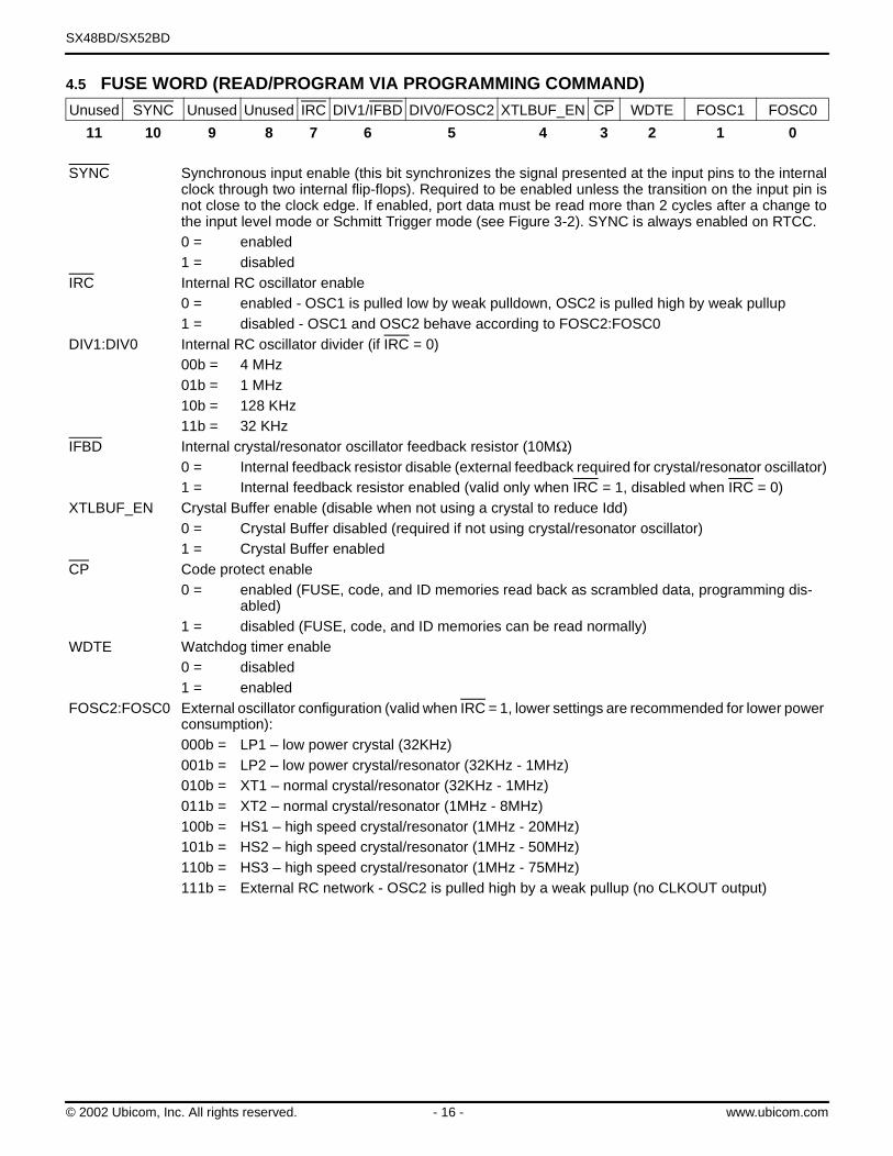
4.5 FUSE WORD (READ/PROGRAM VIA PROGRAMMING COMMAND) Unused SYNC Unused Unused IRC DIV1/IFBD DIV0/FOSC2 XTLBUF_EN CP WDTE FOSC1 FOSC0
11 10 9 8 7 6 5 4 3 2 1 0
SYNC Synchronous input enable (this bit synchronizes the signal presented at the input pins to the internalclock through two internal flip-flops). Required to be enabled unless the transition on the input pin isnot close to the clock edge. If enabled, port data must be read more than 2 cycles after a change tothe input level mode or Schmitt Trigger mode (see Figure 3-2). SYNC is always enabled on RTCC.0 = enabled1 = disabled
IRC Internal RC oscillator enable0 = enabled - OSC1 is pulled low by weak pulldown, OSC2 is pulled high by weak pullup1 = disabled - OSC1 and OSC2 behave according to FOSC2:FOSC0
DIV1:DIV0 Internal RC oscillator divider (if IRC = 0)00b = 4 MHz01b = 1 MHz10b = 128 KHz11b = 32 KHz
IFBD Internal crystal/resonator oscillator feedback resistor (10MΩ)0 = Internal feedback resistor disable (external feedback required for crystal/resonator oscillator)1 = Internal feedback resistor enabled (valid only when IRC = 1, disabled when IRC = 0)
XTLBUF_EN Crystal Buffer enable (disable when not using a crystal to reduce Idd)0 = Crystal Buffer disabled (required if not using crystal/resonator oscillator)1 = Crystal Buffer enabled
CP Code protect enable0 = enabled (FUSE, code, and ID memories read back as scrambled data, programming dis-
abled)1 = disabled (FUSE, code, and ID memories can be read normally)
WDTE Watchdog timer enable0 = disabled1 = enabled
FOSC2:FOSC0 External oscillator configuration (valid when IRC = 1, lower settings are recommended for lower power consumption):000b = LP1 – low power crystal (32KHz)001b = LP2 – low power crystal/resonator (32KHz - 1MHz)010b = XT1 – normal crystal/resonator (32KHz - 1MHz)011b = XT2 – normal crystal/resonator (1MHz - 8MHz)100b = HS1 – high speed crystal/resonator (1MHz - 20MHz)101b = HS2 – high speed crystal/resonator (1MHz - 50MHz)110b = HS3 – high speed crystal/resonator (1MHz - 75MHz)111b = External RC network - OSC2 is pulled high by a weak pullup (no CLKOUT output)
© 2002 Ubicom, Inc. All rights reserved. - 16 - www.ubicom.com
SX48BD/SX52BD
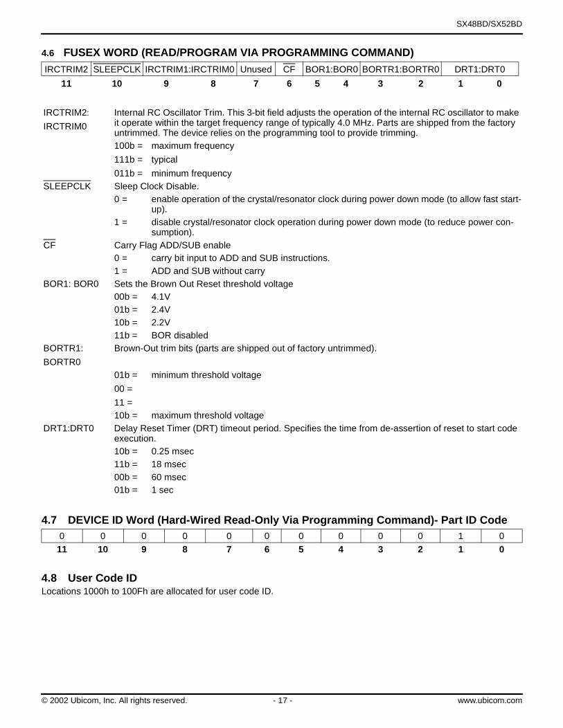
4.6 FUSEX WORD (READ/PROGRAM VIA PROGRAMMING COMMAND)
4.7 DEVICE ID Word (Hard-Wired Read-Only Via Programming Command)- Part ID Code
4.8 User Code IDLocations 1000h to 100Fh are allocated for user code ID.
IRCTRIM2 SLEEPCLK IRCTRIM1:IRCTRIM0 Unused CF BOR1:BOR0 BORTR1:BORTR0 DRT1:DRT0
11 10 9 8 7 6 5 4 3 2 1 0
IRCTRIM2:
IRCTRIM0
Internal RC Oscillator Trim. This 3-bit field adjusts the operation of the internal RC oscillator to make it operate within the target frequency range of typically 4.0 MHz. Parts are shipped from the factory untrimmed. The device relies on the programming tool to provide trimming.100b =
111b =
011b =
maximum frequency
typical
minimum frequencySLEEPCLK Sleep Clock Disable.
0 = enable operation of the crystal/resonator clock during power down mode (to allow fast start-up).
1 = disable crystal/resonator clock operation during power down mode (to reduce power con-sumption).
CF Carry Flag ADD/SUB enable0 = carry bit input to ADD and SUB instructions.1 = ADD and SUB without carry
BOR1: BOR0 Sets the Brown Out Reset threshold voltage00b = 4.1V01b = 2.4V10b = 2.2V11b = BOR disabled
BORTR1:
BORTR0
Brown-Out trim bits (parts are shipped out of factory untrimmed).
01b =
00 =
11 =
minimum threshold voltage
10b = maximum threshold voltageDRT1:DRT0 Delay Reset Timer (DRT) timeout period. Specifies the time from de-assertion of reset to start code
execution.10b = 0.25 msec11b = 18 msec00b = 60 msec01b = 1 sec
0 0 0 0 0 0 0 0 0 0 1 0
11 10 9 8 7 6 5 4 3 2 1 0
© 2002 Ubicom, Inc. All rights reserved. - 17 - www.ubicom.com

SX48BD/SX52BD
5.0 MEMORY ORGANIZATION
5.1 Program MemoryThe program memory is organized as 4K, 12-bit widewords. The program memory words are addressedsequentially by a binary program counter. Upon reset, theprogram counter is initialized with 0FFFh. If there is nobranch operation, it will increment to the maximum valuepossible for the device and roll over and begin again.
Internally, the program memory has a semi-transparentpage structure. A page is composed of 512 contiguousprogram memory words. The lower nine bits of the pro-gram counter are zeros at the first address of a page andones at the last address of a page. This page structurehas no effect on the program counter. The programcounter will freely increment through the page bound-aries.
5.1.1 Program Counter
The program counter contains the 12-bit address of theinstruction to be executed. The lower eight bits of the pro-gram counter are contained in the PC register (02h), andthe three upper bits are specified by the STATUS register(PA0, PA1, PA2). Bit 8 is not accessible. Changing theSTATUS bits is necessary to cause jumps and subroutinecalls across program memory page boundaries. Prior tothe execution of a branch operation, the user programmust initialize the upper bits of the STATUS register tocause a branch to the desired page. An alternativemethod is to use the PAGE instruction, which automati-cally causes branch to the desired page, based on thevalue specified in the operand field.
5.1.2 Subroutine Stack
The subroutine stack consists of eight 12-bit save regis-ters. A physical transfer of register contents from the pro-gram counter to the stack or vice versa, and within thestack, occurs on all operations affecting the stack, prima-rily calls and returns. The stack is physically and logicallyseparate from data RAM. The program cannot read orwrite the stack.
5.2 Data MemoryThe data memory is a RAM-based register set consistingof 262 general-purpose registers and nine special-pur-pose registers. All of these registers are eight bits wide.
The data memory is organized into 16 banks, designatedBank 0 through Bank F, each containing 16 registers,plus an additional bank of 16 “global” registers. Becausethe registers are organized into banks or “files,” thesememory-mapped registers are called “file registers.”
5.2.1 Addressing Modes/FSR
Each SX instruction that accesses a data memory regis-ter contains a 5-bit field in the instruction opcode thatspecifies the register to be accessed. The abbreviation“fr” (file register) represents the 5-bit register addressdesignator. For example, the instruction description “movfr,W” means that a 5-bit value or label must be substi-tuted for “fr” in the instruction, such as “mov $0F,W” (tomove the contents of the working register W into file reg-ister 0Fh).
There are three different addressing modes, called theindirect, direct, and semi-direct modes. The addressingmode used for register access depends on the 5-bit “fr”value used in the instruction:
• indirect mode: fr = 00h• direct mode (fr bit 4 = 0): fr = 01h through 0Fh• semi-direct mode (fr bit 4 = 1): fr = 10h through 1FhFigure 5-1 illustrates the data memory addressingscheme.
For indirect addressing (fr=00), the File Select Register(FSR) specifies the register to be accessed. FSR is an 8-bit, memory-mapped register (at address 04h) whichserves as an 8-bit pointer into data memory for indirectaddressing. In this mode, the global register bank andBank 1 through Bank F are accessible. Bank 0 is notaccessible.
For direct addressing (fr=01-0F), the value of “fr” itselfspecifies the register to be accessed, and the FSR regis-ter is ignored. For this addressing mode, only the globalregister bank is accessible. To gain access to any otherbank, you must use either indirect or semi-directaddressing.
For semi-direct addressing (fr=10-1F), the bank numberis selected by the four high-order bits of FSR, and theregister within that bank is selected by the four low-orderbits of “fr.” In other words, the register address isobtained by combining the four high-order bits of FSRwith the four low-order bits of “fr”. In this addressingmode, the low-order bits of FSR are ignored. Bank 0through Bank F are accessible, but the global registerbank is not accessible.
Figure 5-1 shows how register addressing works in theindirect, direct, and semi-direct modes. The 16 globalregisters are always accessible by direct addressing,regardless of what is contained in the FSR register. Theglobal registers are also accessible with indirect address-ing, but they are not accessible with semi-direct address-ing. Of the 16 global registers, nine are special-purposeregisters (RTCC, PC, STATUS, and so on), and six aregeneral-purpose registers. Location 00 is used for indi-rect addressing (INDF). All of the registers in Bank 0though Bank F are general-purpose registers.
To change the contents of the FSR register, the programcan either write an eight-bit value to the FSR register oruse the “bank” instruction. The “bank” instruction writesbits 4, 5, and 6 in the FSR register. Bit 7 of FSR is used toselect the upper or lower “bank” of memory banks. Thus,to change from one upper bank to another, only a single“bank” instruction is required. To change from one upperbank to a lower bank, the “bank” instruction must be fol-lowed by “setb FSR.7”.
© 2002 Ubicom, Inc. All rights reserved. - 18 - www.ubicom.com

SX48BD/SX52BD
Figure 5-1. Register Access Modes
00h
01h
02h
03h
04h
05h
06h
07h
08h
09h
0Ah
0Bh
0Ch
0Dh
0Eh
0Fh
10h
11h
12h
13h
14h
15h
16h
17h
18h
19h
1Ah
1Bh
1Ch
1Dh
1Eh
1Fh
Indirect Addressing
Direct Addressing
Semi-Direct Addressing
X X X X
FSR
5-Bit “fr” Value of Instruction
FSR bits 7:0 select one of the registers in the global register set or a register in Bank 1 through Bank F. Bank 0 is not accessible.
“fr” bits 3:0 select one of 15 registers in the global register set. The FSR register is ignored. Bank 0 through Bank F are not accessible.
FSR bits 7:4 select one of 16 banks, and “fr” bits 3:0 select one of 16 registers in that bank. The four low-order bits of FSR are ignored. All 256 registers in Bank 0 through Bank F are accessible. The global registers are not accessible.
Bank 0 Bank 1 Bank 2 Bank E Bank F
F0F1F2F3F4F5F6F7F8F9FAFBFCFDFEFF
E0E1E2E3E4E5E6E7E8E9EAEBECEDEEEF
101112131415161718191A1B1C1D1E1F
202122232425262728292A2B2C2D2E2F
00 0102030405060708090A0B0C0D0E0F
00 INDF01 RTCC 02 PC 03 STATUS 04 FSR 05 RA 06 RB 07 RC 08 RD 09 RE 0A0B0C0D0E0F
GlobalRegisters
fr
1
fr
0
UserConfigured Modified by BANK instruction
FSR
© 2002 Ubicom, Inc. All rights reserved. - 19 - www.ubicom.com

SX48BD/SX52BD
5.2.2 Register Access Examples
Here is an example of an instruction that uses directaddressing:
inc $0F ;increment file register 0Fh
This instruction increments the contents of file register0Fh in the global register bank. It does not matter what iscontained in the FSR register.
To gain access to any register outside of the global regis-ter bank, it is necessary to use semi-direct or indirectaddressing. In that case, you need to make sure that theFSR register contains the correct value for accessing thedesired bank.
Here are 2 examples that use semi-direct addressing:
mov W,#$F0 ;load W with F0h mov FSR,W ;load W into FSR (Bank F) inc $1F ;increment file register FFh
Or, to access bank 0,
mov W,#$00 ;load W with 00h mov FSR,W ;load W into FSR (Bank 0) inc $1F ;increment file register 0Fh
In these examples, “FSR” is a label that represents thevalue 04h, which is the address of the FSR register in theglobal register bank. Note that the FSR register is itself amemory-mapped global register, which is always acces-sible using direct addressing.
The “banked” data memory is divided into upper andlower blocks, each consisting of 8 banks of data memory.The range for the lower block is from $00 to $7F, whilethe rage for the upper block is from $80 to $FF. Bit 7 ofthe FSR is used to select the upper or lower block. TheBANK instruction is used to select the bank within thatblock.
To use the “bank” instruction, in the syntax of the assem-bly language, you specify an 8-bit value that correspondsto the desired bank number. The assembler encodes bits4, 5, and 6 of the specified value into the instructionopcode and ignores bit 7 and the low-order bits. Forexample, if another lower bank was being used to incre-ment file register 2Fh, you could use the followinginstructions: bank $20 ;select Bank 2 in FSRinc $1F ;increment register 2F
Note that the “bank” instruction only modifies bits 4, 5,and 6 the FSR register. Therefore, to change from alower block to an upper block bank, the “bank” instructionwill not work. Instead, you need to write the whole FSRregister using code such as the following:
mov W,#$80 ;load W with 80h mov FSR,W ;select Bank 8 in FSR
Another approach is to set bit 7 of the FSR register indi-vidually after the “bank” instruction to address an upper block bank.bank $80 ;set bits in 4, 5, and 6 FSRsetb FSR.7 ;select Bank 8 in FSR
To change from an upper block to a lower block bank, bit7 of FSR must be cleared.
With indirect addressing, you specify the full 8-bitaddress of the register using FSR as a pointer. Thisaddressing mode provides the flexibility to access differ-ent registers or multiple registers using the same instruc-tion in the program.
You invoke indirect addressing by using fr=00h. Forexample:
mov W,#$F5 ;load W with F5hmov $04,W ;move value F5h into FSRmov W,#$01 ;load W with 01hmov $00,W ;move value 01h into register F5h
In the second “mov” instruction, FSR is loaded with thedesired 8-bit register address. In the fourth “mov” instruc-tion, fr = 00, so the device looks at FSR and moves theresult to the register addressed by FSR, which is the reg-ister at F5h (Bank F, register number 5).
A practical example that uses indirect addressing is thefollowing program, which clears the upper eight registersin the global register bank and the upper 8 registers in allbanks from Bank 1 through Bank F:
clr FSR ;clear FSR to 00h (at address 04h):loop setb FSR.3 ;set FSR bit 3clr $00 ;clear register pointed to by FSRincsz FSR ;increment FSR and test
;skip jmp if 00hjmp:loop ;jump back and clear next reg.
This program initially clears FSR to 00h. At the beginningof the loop, it sets bit 3 of FSR so that it starts at 08h. The“clr $00” instruction clears the register pointed to by FSR(initially, the file register at 08h in the global registerbank). Then the program increments FSR and clearsconsecutive file registers, always in the upper half ofeach bank: (08h, 09h, 0Ah... 0Fh, 18h, 19h... FFh). Theloop ends when FSR wraps back to 00h.
For addresses from 01h through 0Fh, the global registerbank is accessed. For higher addresses, Bank 1 throughBank F are accessed. This program does not affect Bank0, which is not accessible in the indirect addressingmode. Bank 0 can be accessed only using the semi-direct mode.
© 2002 Ubicom, Inc. All rights reserved. - 20 - www.ubicom.com

SX48BD/SX52BD
6.0 POWER DOWN MODEThe power down mode is entered by executing theSLEEP instruction.
In power down mode, only the Watchdog Timer (WDT)and SLEEPCLOCK are active, if enabled. The operationclock can be enabled or disabled during this mode, byusing the SLEEPCLK bit of the FUSEX register. If theWatchdog Timer is enabled, upon execution of theSLEEP instruction, the Watchdog Timer is cleared, theTO (time out) bit is set in the STATUS register, and thePD (power down) bit is cleared in the STATUS register.
There are three different ways to exit from the powerdown mode:
1. A timer overflow signal from the Watchdog Timer (WDT).
2. A valid transition on any of the Multi-Input Wakeup pins (Port B pins).
3. An external reset input on the MCLR pin. The states of registers (upon wakeup) are described inSection 14.0.
To achieve the lowest possible power consumption, theWatchdog Timer should be disabled (the sleep clockshould be disabled) and the device should exit the powerdown mode through the (Multi-Input Wakeup) MIWU pinsor an external reset. In addition, the SLEEPCLOCKshould be disabled during the power down mode.
Bit 11 of the FUSEX can be used to enable (clear bit to 0)the clock operation during the power down mode (to
allow fast clock start-up upon exiting the power downmode).
6.1 Multi-Input WakeupMulti-Input Wakeup is one way of causing the device toexit the power down mode. Port B is used to support thisfeature. The WKEN_B register (Wakeup Enable Regis-ter) allows any Port B pin or combination of pins to causethe wakeup. Clearing a bit in the WKEN_B registerenables the wakeup on the corresponding Port B pin. Ifmulti-input wakeup is selected to cause a wakeup, thetrigger condition on the selected pin can be either risingedge (low to high) or falling edge (high to low). TheWKED_B register (Wakeup Edge Select) selects thedesired transition edge. Setting a bit in the WKED_B reg-ister selects the falling edge on the corresponding Port B.Resetting the bit selects the rising edge. The WKEN_Band WKED_B registers are set to FFh upon reset.
Once a valid transition occurs on the selected pin, theWKPND_B register (Wakeup Pending Register) latchesthe transition in the corresponding bit position. A logic ‘1’indicates the occurrence of the selected trigger edge onthe corresponding Port B pin. The WKPND_B comes upwith undefined value upon reset. The user program mustclear the WKPND_B register prior to enabling the inter-rupt.
Upon exiting the power down mode, the Multi-InputWakeup logic causes program counter to branch to themaximum program memory address (same as reset).
Figure 6-1 shows the Multi-Input Wakeup block diagram.
Figure 6-1. Multi-Input Wakeup Block Diagram
W
Inte
rnal
Dat
a B
us
MODE
Wake-up: Exit Power Down
8
8
RB7 RB6 RB1 RB0
WKED_B
WKPND_B
WKEN_B
MODE=09/19
MO
DE
=0B
/1B M
OD
E=
0A/1
A
Port BConfiguredas Input
0 1
8
0 = Enable1 = Disable
© 2002 Ubicom, Inc. All rights reserved. - 21 - www.ubicom.com
SX48BD/SX52BD
6.2 Port B MIWU/Interrupt ConfigurationThe WKPND_B register comes up with a random valueupon reset. The user program must clear the registerprior to enabling the wake-up condition or interrupts. Theproper initialization sequence is:
1. Select the desired edge (through WKED_B register).2. Clear the WKPND_B register.3. Enable the Wakeup condition (through WKEN_B regis-
ter).Below is an example of how to read the WKPND_B regis-ter to determine which Port B pin caused the wakeup orinterrupt, and to clear the WKPND_B register:
The final “mov” instruction in this example performs anexchange of data between the working register (W) andthe WKPND_B register. This exchange occurs only withaccesses to the WKPND_B and CMP_B registers. Other-wise, the “mov” instruction does not perform anexchange, but only moves data from the source to thedestination.
Here is an example of a program segment that config-ures the RB0, RB1, and RB2 pins to operate as Multi-Input Wakeup/Interrupt pins, sensitive to falling edges:
To prevent false interrupts, the enabling step (clearingbits in WKEN_B) should be done as the last step in asequence of Port B configuration steps.
After this program segment is executed, the device canreceive interrupts on the RB0, RB1, and RB2 pins. If thedevice is put into the power down mode (by executing aSLEEP instruction), the device can then receive wakeupsignals on those same pins.
mov W, #$19 ;prepare to exchange WKPND_B ;with W (can also use $09)
mov M, Wclr Wmov !RB,W ;W contains WKPND_B
;contents of W exchanged;with contents of WKPND_B
mov
mov
W,#$1F
M,W
;prepare to write port data ;direction registers
mov W,#$07 ;load W with the value 07hmov !RB,W ;configure RB0-RB2 to be inputs
mov
mov
W,#$1A
M,W
;prepare to write WKED_B ;(edge) register
mov W,#$07 ;load W with the value 07hmov !RB,W ;configure RB0-RB2 to sense
;falling edges
mov W,#$19 ;prepare to access WKPND_Bmov M,W ;(pending) registermov W,#$00 ;clear Wmov !RB,W ;clear all wakeup pending flags
mov
mov
W,#$1B
M,W
;prepare to write WKEN_B (enable);register
mov W,#$F8 ;load W with the value F8hmov !RB,W ;enable RB0-RB2 to operate as
;wakeup inputs
© 2002 Ubicom, Inc. All rights reserved. - 22 - www.ubicom.com
SX48BD/SX52BD
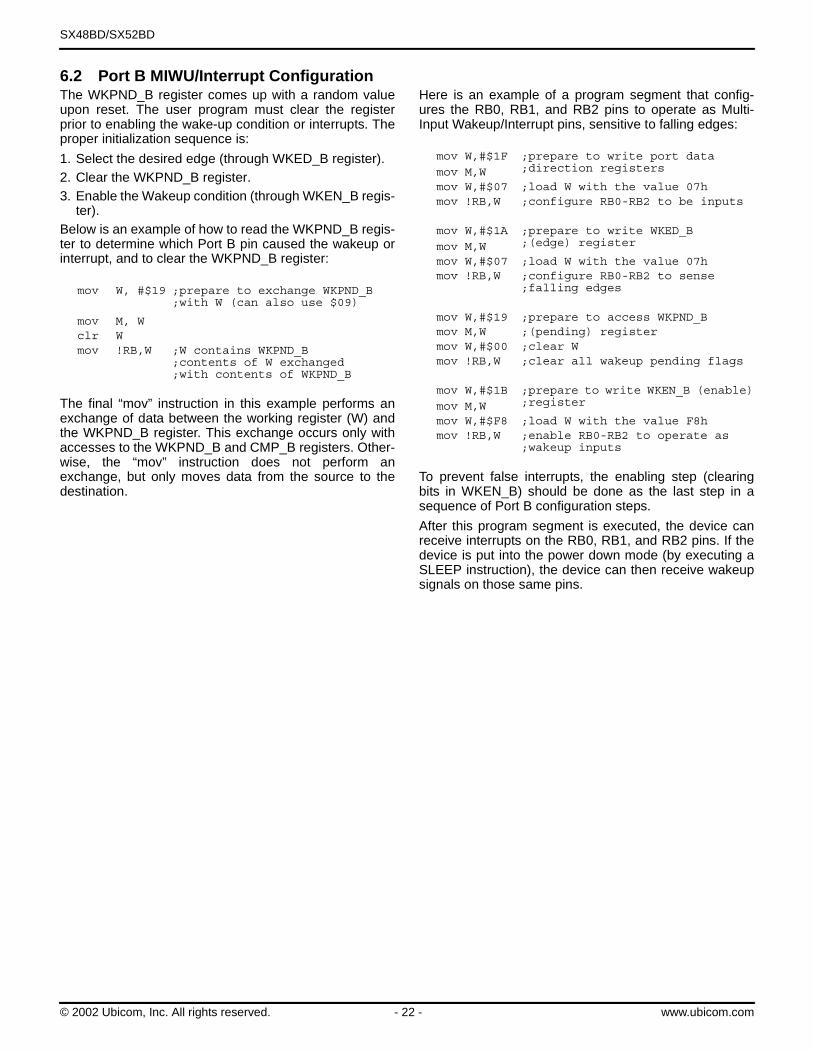
7.0 INTERRUPT SUPPORTThe device supports both internal and external maskableinterrupts. The internal interrupt is generated as a resultof the RTCC rolling over from FFh to 00h. This interruptsource has an associated enable bit located in theOPTION register and pending flag bit in the Timer T1Control B register. In addition, timers T1 and T2 eachhave three interrupt sources associated with counteroverflow, compare match, and input capture.
Port B provides the source for eight external softwareselectable, edge sensitive interrupts, when the device isnot in the power down mode. These interrupt sourcesshare logic with the Multi-Input Wakeup circuitry. TheWKEN_B register allows interrupt from Port B to be indi-vidually enabled or disabled. Clearing a bit in the
WKEN_B register enables the interrupt on the corre-sponding Port B pin. The WKED_B selects the transitionedge to be either positive or negative. The WKEN_B andWKED_B registers are set to FFh upon reset. Setting abit in the WKED_B register selects the falling edge whileclearing the bit selects the rising edge on the correspond-ing Port B pin.
The WKPND_B register serves as the external interruptpending register.
The WKPND_B register comes up with a random valueupon reset. The user program must clear the WKPND_Bregister prior to enabling the interrupt.
Figure 7-1. Interrupt Structure
RTCCWKED_B
Inte
rna
l Data
Bu
s
WKED_B
WKPND_BWKPND_B
From MODE(MODE = 09/19)
OPTIONRTE_IE
WKEN_B
1 = Ext. Interrupt through Port B0 = Sleep Mode, no Ext. Interrupt
STATUS
Port B PIN
Interrupt
PC000
Overflow
Device-SpecificInterrupt Sources(e.g. Timer T1)
RegisterPD Flag
From MODE(MODE = 0A/1A)
PC, STATUS, FSR, W, MODE Interrupt Stack
© 2002 Ubicom, Inc. All rights reserved. - 23 - www.ubicom.com

SX48BD/SX52BD
All interrupts are global in nature; that is, no interrupt haspriority over another. Interrupts are handled sequentially.Figure 7-2 shows the interrupt processing sequence.Once an interrupt is acknowledged, all subsequent inter-rupts are disabled until return from servicing the currentinterrupt. The PC is pushed onto the single level interruptstack, and the contents of the FSR, STATUS, MODE, andW registers are saved in their corresponding shadow reg-isters. The status bits PA2, PA1, and PA0 are clearedafter STATUS has been saved in its shadow register. Theinterrupt logic has its own single-level stack and is notpart of the CALL subroutine stack. The vector for theinterrupt service routine is address 0.
Once in the interrupt service routine, the user programmust poll all interrupt pending bits to determine thesource of the interrupt. The interrupt service routineshould clear the corresponding interrupt pending flag.
Normally it is a requirement for the user program to pro-cess every interrupt without missing any. To ensure this,the longest path through the interrupt routine must takeless time than the shortest possible delay between inter-rupts.
Using more than one interrupt, such as multiple externalinterrupts or both RTCC and external interrupts, canresult in missed or, at best, jittery interrupt handlingshould one occur during the processing of another. Whenhandling external interrupts, the interrupt routine shouldclear at least one pending register bit. The bit that iscleared should represent the interrupt being handled inorder for the next interrupt to trigger.
Upon return from the interrupt service routine, the con-tents of PC, FSR, STATUS, MODE, and W registers arerestored from their corresponding shadow registers. Theinterrupt service routine should end with instructions suchas RETI or RETIW. RETI pops the interrupt stack and thespecial shadow registers used for storing W, STATUS,MODE, and FSR (preserved during interrupt handling).RETIW behaves like RETI but also adds W to RTCC. Theinterrupt return instruction enables interrupts.
If a MIWU interrupt occurs during a pre-existing interruptservice routine, the MIWU interrupt flag is set immedi-ately, and the MIWU interrupt is serviced upon comple-tion of the pre-existing interrupt service routine.
Timer interrupt will occur only if the ISR is not executingwhen the interrupt occurs.
Figure 7-2. Interrupt Processing
Interrupt
PC
RETI
PC PC
WRegister
000h
Address 000h
ProgramMemory Interrupt
Service Routine
STATUSRegister
FSRRegister
WShadow Register
STATUSShadow Register
FSRShadow Register
WRegister
STATUSRegister
FSRRegister
WShadow Register
STATUSShadow Register
FSRShadow Register
StackInterrupt
Stack
Note:The interrupt logic has its own single-levelstack and is not part of the CALL subroutine stack.
MODERegister
MODEShadow Register
MODERegister
MODEShadow Register
© 2002 Ubicom, Inc. All rights reserved. - 24 - www.ubicom.com
SX48BD/SX52BD
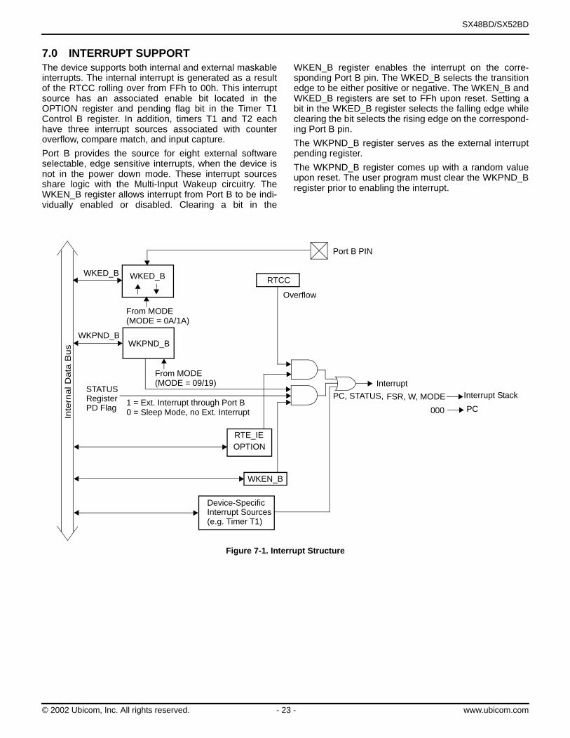
8.0 OSCILLATOR CIRCUITSThe device supports several user-selectable oscillatormodes. The oscillator modes are selected by program-ming the appropriate values into the FUSE Word register.These are the different oscillator modes offered:
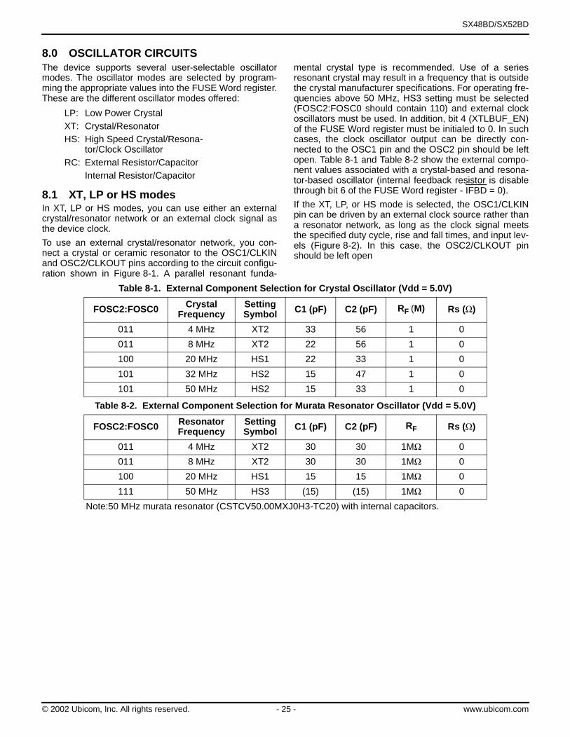
8.1 XT, LP or HS modesIn XT, LP or HS modes, you can use either an externalcrystal/resonator network or an external clock signal asthe device clock.
To use an external crystal/resonator network, you con-nect a crystal or ceramic resonator to the OSC1/CLKINand OSC2/CLKOUT pins according to the circuit configu-ration shown in Figure 8-1. A parallel resonant funda-
mental crystal type is recommended. Use of a seriesresonant crystal may result in a frequency that is outsidethe crystal manufacturer specifications. For operating fre-quencies above 50 MHz, HS3 setting must be selected(FOSC2:FOSC0 should contain 110) and external clockoscillators must be used. In addition, bit 4 (XTLBUF_EN)of the FUSE Word register must be initialed to 0. In suchcases, the clock oscillator output can be directly con-nected to the OSC1 pin and the OSC2 pin should be leftopen. Table 8-1 and Table 8-2 show the external compo-nent values associated with a crystal-based and resona-tor-based oscillator (internal feedback resistor is disablethrough bit 6 of the FUSE Word register - IFBD = 0).
If the XT, LP, or HS mode is selected, the OSC1/CLKINpin can be driven by an external clock source rather thana resonator network, as long as the clock signal meetsthe specified duty cycle, rise and fall times, and input lev-els (Figure 8-2). In this case, the OSC2/CLKOUT pinshould be left open
LP: Low Power CrystalXT: Crystal/ResonatorHS: High Speed Crystal/Resona-
tor/Clock OscillatorRC: External Resistor/Capacitor
Internal Resistor/Capacitor
Table 8-1. External Component Selection for Crystal Oscillator (Vdd = 5.0V)
FOSC2:FOSC0 CrystalFrequency
Setting Symbol C1 (pF) C2 (pF) RF (M) Rs (Ω)
011 4 MHz XT2 33 56 1 0
011 8 MHz XT2 22 56 1 0
100 20 MHz HS1 22 33 1 0
101 32 MHz HS2 15 47 1 0
101 50 MHz HS2 15 33 1 0
Table 8-2. External Component Selection for Murata Resonator Oscillator (Vdd = 5.0V)
FOSC2:FOSC0 ResonatorFrequency
Setting Symbol C1 (pF) C2 (pF) RF Rs (Ω)
011 4 MHz XT2 30 30 1MΩ 0
011 8 MHz XT2 30 30 1MΩ 0
100 20 MHz HS1 15 15 1MΩ 0
111 50 MHz HS3 (15) (15) 1MΩ 0
Note:50 MHz murata resonator (CSTCV50.00MXJ0H3-TC20) with internal capacitors.
© 2002 Ubicom, Inc. All rights reserved. - 25 - www.ubicom.com
SX48BD/SX52BD
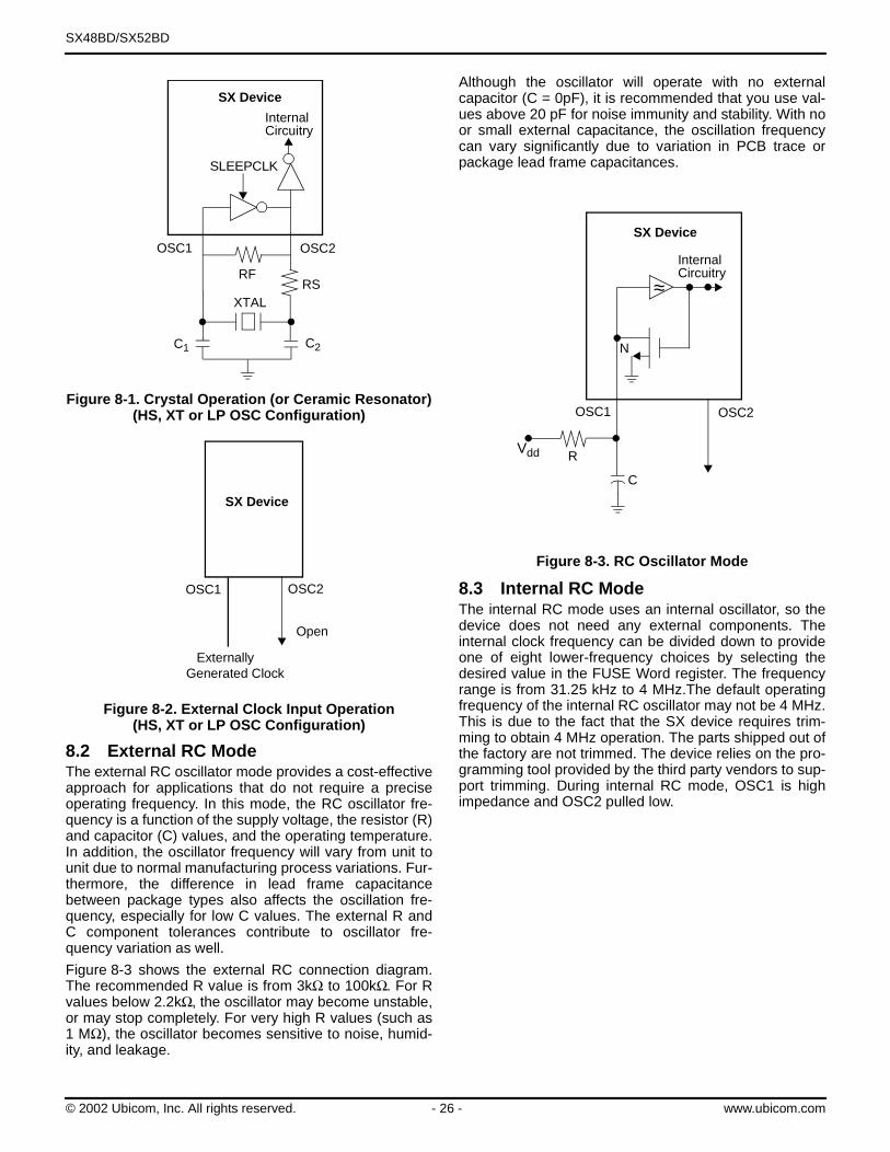
8.2 External RC ModeThe external RC oscillator mode provides a cost-effectiveapproach for applications that do not require a preciseoperating frequency. In this mode, the RC oscillator fre-quency is a function of the supply voltage, the resistor (R)and capacitor (C) values, and the operating temperature.In addition, the oscillator frequency will vary from unit tounit due to normal manufacturing process variations. Fur-thermore, the difference in lead frame capacitancebetween package types also affects the oscillation fre-quency, especially for low C values. The external R andC component tolerances contribute to oscillator fre-quency variation as well.
Figure 8-3 shows the external RC connection diagram.The recommended R value is from 3kΩ to 100kΩ. For Rvalues below 2.2kΩ, the oscillator may become unstable,or may stop completely. For very high R values (such as1 MΩ), the oscillator becomes sensitive to noise, humid-ity, and leakage.
Although the oscillator will operate with no externalcapacitor (C = 0pF), it is recommended that you use val-ues above 20 pF for noise immunity and stability. With noor small external capacitance, the oscillation frequencycan vary significantly due to variation in PCB trace orpackage lead frame capacitances.
8.3 Internal RC ModeThe internal RC mode uses an internal oscillator, so thedevice does not need any external components. Theinternal clock frequency can be divided down to provideone of eight lower-frequency choices by selecting thedesired value in the FUSE Word register. The frequencyrange is from 31.25 kHz to 4 MHz.The default operatingfrequency of the internal RC oscillator may not be 4 MHz.This is due to the fact that the SX device requires trim-ming to obtain 4 MHz operation. The parts shipped out ofthe factory are not trimmed. The device relies on the pro-gramming tool provided by the third party vendors to sup-port trimming. During internal RC mode, OSC1 is highimpedance and OSC2 pulled low.
Figure 8-1. Crystal Operation (or Ceramic Resonator) (HS, XT or LP OSC Configuration)
Figure 8-2. External Clock Input Operation (HS, XT or LP OSC Configuration)
SX Device
RF
XTAL
OSC2OSC1
C1 C2
InternalCircuitry
SLEEPCLK
RS
OSC1 OSC2
SX Device
ExternallyGenerated Clock
Open
Figure 8-3. RC Oscillator Mode
Vdd R
C
InternalCircuitry
OSC2OSC1
N
~~
SX Device
© 2002 Ubicom, Inc. All rights reserved. - 26 - www.ubicom.com

SX48BD/SX52BD
9.0 REAL TIME CLOCK/COUNTER (RTCC)/WATCHDOG TIMERThe device contains an 8-bit Real Time Clock/Counter(RTCC) and an 8-bit Watchdog Timer (WDT). An 8-bitprogrammable prescaler extends the RTCC to 16 bits. Ifthe prescaler is not used for the RTCC, it can serve as apostscaler for the Watchdog Timer. Figure 9-1 shows theRTCC and WDT block diagram.
9.1 RTCC RTCC is an 8-bit real-time timer that is incremented onceby the internal instruction cycle clock or from a transitionon the RTCC pin. The on-board prescaler can be used toextend the RTCC counter to 16 bits.
To select the internal clock source, bit 5 of the OPTIONregister should be cleared. In this mode, RTCC is incre-mented at each instruction cycle unless the prescaler isselected to increment the counter.
To select the external clock source, bit 5 of the OPTIONregister must be set. In this mode, the RTCC pin is sam-pled on each rising edge of the OSC1 pin (the signal fre-quency at the RTTC pin must be less half the frequencyon OSC1). By using bit 4 of the OPTION register, thetransition can be programmed to be either a falling edgeor rising edge. Setting the control bit selects the fallingedge to increment the counter. Clearing the bit selectsthe rising edge.
The RTCC generates an interrupt (if enabled) as a resultof an RTCC rollover from FFh to 00h. Bit 7 of the TimerT1 Control B register is an interrupt pending flag (RTC-COV) associated with this event. The program shouldread this flag to determine any rollover occurrence. Writ-ing to the RTCC also clears the prescaler if it is assignedto the RTCC (bit 3 at OPTION register is cleared).Usingthe “TEST fr” with RTCC (with fr being the RTCC andRTCC clock internally or externally) will not allow theRTCC to increment. The workaround is to use the “MOVW, RTCC” instruction instead.
9.2 Watchdog TimerThe watchdog logic consists of a Watchdog Timer whichshares the same 8-bit programmable prescaler with theRTCC. The prescaler actually serves as a postscaler ifused in conjunction with the WDT, in contrast to its use asa prescaler with the RTCC. The WDT is clocked by it’sown internal RC oscillator.
The Watchdog oscillator has a nominal operating fre-quency of 16 kHz, or a period of 62.5 microseconds. Atthis rate, the 8-bit counter counts from 00h to FFh in 16milliseconds. In the default configuration (prescalerassigned to WDT, with divide rate set to 1:128), the appli-cation program needs to execute a “CLR !WDT” instruc-tion at least once every 2 seconds to prevent a Watchdogreset (if the WDTE bit in the FUSE register is set to 1).
9.3 The Prescaler The 8-bit prescaler may be assigned to either the RTCCor the WDT through the PSA bit (bit 3 of the OPTION reg-ister). Setting the PSA bit assigns the prescaler to theWDT. If assigned to the WDT, the WDT clocks the pres-caler and the prescaler divide rate is selected by thePS0, PS1, and PS2 bits located in the OPTION register.Clearing the PSA bit assigns the prescaler to the RTCC.Once assigned to the RTCC, the prescaler clocks theRTCC and the divide rate is selected by the PS0, PS1,and PS2 bits in the OPTION register. The prescaler is notmapped into the data memory, so run-time access is notpossible.
The prescaler cannot be assigned to both the RTCC andWDT simultaneously.
© 2002 Ubicom, Inc. All rights reserved. - 27 - www.ubicom.com

SX48BD/SX52BD
Figure 9-1. RTCC and WDT Block Diagram
WDTE (from FUSE Word)
RTCC pin
MUX
8-Bit Prescaler
MUX (8 to 1)
8-Bits
WDT TimeoutData Bus
WDT
MUX
MUX
RTCC
MUX
FOSCRST
RTE_ESPSAPS2PS1PS0
OPTIONRegister
RTCC RolloverInterrupt
RTE_IERTW
RTCC Interrupt Enable
Interruptto CPU
Pending Flag(RTCCOV bit inT1CNTB Register,SX48/52BD only)
© 2002 Ubicom, Inc. All rights reserved. - 28 - www.ubicom.com
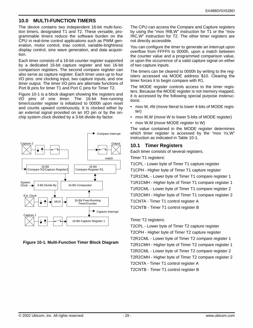
SX48BD/SX52BD
10.0 MULTI-FUNCTION TIMERSThe device contains two independent 16-bit multi-func-tion timers, designated T1 and T2. These versatile, pro-grammable timers reduce the software burden on theCPU in real-time control applications such as PWM gen-eration, motor control, triac control, variable-brightnessdisplay control, sine wave generation, and data acquisi-tion.
Each timer consists of a 16-bit counter register supportedby a dedicated 16-bit capture register and two 16-bitcomparison registers. The second compare register canalso serve as capture register. Each timer uses up to fourI/O pins: one clocking input, two capture inputs, and onetimer output. The timer I/O pins are alternate functions ofPort B pins for timer T1 and Port C pins for Timer T2.
Figure 10-1 is a block diagram showing the registers andI/O pins of one timer. The 16-bit free-runningtimer/counter register is initialized to 0000h upon resetand counts upward continuously. It is clocked either byan external signal provided on an I/O pin or by the on-chip system clock divided by a 3-bit divide-by factor.
The CPU can access the Compare and Capture registersby using the “mov !RB,W” instruction for T1 or the “mov!RC,W” instruction for T2. The other timer registers arenot directly accessible.
You can configure the timer to generate an interrupt uponoverflow from FFFFh to 0000h, upon a match betweenthe counter value and a programmed comparison value,or upon the occurrence of a valid capture signal on eitherof two capture inputs.
The timers can be cleared to 0000h by writing to the reg-isters accessed via MODE address $10. Clearing thetimer forces it to begin compare with R1.
The MODE register controls access to the timer regis-ters. Because the MODE register is not memory mapped,it is accessed by the following special purpose insteruc-tions:
• mov M, #lit (move literal to lower 4-bits of MODE regis-ter)
• mov M,W (move W to lower 5-bits of MODE register)• mov W,M (move MODE register to W)The value contained in the MODE register determineswhich timer register is accessed by the “mov !rx,W”instruction as indicated in Table 10-1.
10.1 Timer RegistersEach timer consists of several registers.
Timer T1 registers:
T1CPL - Lower byte of Timer T1 capture register
T1CPH - Higher byte of Timer T1 capture register
T1R1CML - Lower byte of Timer T1 compare register 1
T1R1CMH - Higher byte of Timer T1 compare register 1
T1R2CML - Lower byte of Timer T1 compare register 2
T1R2CMH - Higher byte of Timer T1 compare register 2
T1CNTA - Timer T1 control register A
T1CNTB - Timer T1 control register B
Timer T2 registers:
T2CPL - Lower byte of Timer T2 capture register
T2CPH - Higher byte of Timer T2 capture register
T2R1CML - Lower byte of Timer T2 compare register 1
T2R1CMH - Higher byte of Timer T2 compare register 1
T2R2CML - Lower byte of Timer T2 compare register 2
T2R2CMH - Higher byte of Timer T2 compare register 2
T2CNTA - Timer T1 control register A
T2CNTB - Timer T1 control register B
Figure 10-1. Multi-Function Timer Block Diagram
Ext. Clock
Capture 1
Capture 2
3-Bit Divide-By
16-Bit Free-Running
16-Bit Comparator
Compare Register R1Compare R2/Capture Register2
Timer/Counter
16-Bit Capture Register 1
MUX
match
Output
Compare Interrupt
SystemClock
Capture Interrupt
16-Bit 16-Bit
© 2002 Ubicom, Inc. All rights reserved. - 29 - www.ubicom.com
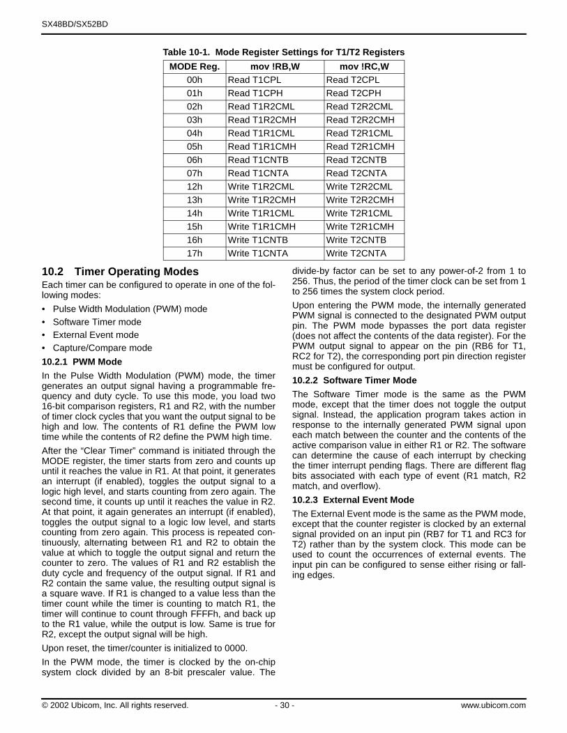
SX48BD/SX52BD
Table 10-1. Mode Register Settings for T1/T2 Registers
10.2 Timer Operating ModesEach timer can be configured to operate in one of the fol-lowing modes:
• Pulse Width Modulation (PWM) mode• Software Timer mode• External Event mode• Capture/Compare mode
10.2.1 PWM Mode
In the Pulse Width Modulation (PWM) mode, the timergenerates an output signal having a programmable fre-quency and duty cycle. To use this mode, you load two16-bit comparison registers, R1 and R2, with the numberof timer clock cycles that you want the output signal to behigh and low. The contents of R1 define the PWM lowtime while the contents of R2 define the PWM high time.
After the “Clear Timer” command is initiated through theMODE register, the timer starts from zero and counts upuntil it reaches the value in R1. At that point, it generatesan interrupt (if enabled), toggles the output signal to alogic high level, and starts counting from zero again. Thesecond time, it counts up until it reaches the value in R2.At that point, it again generates an interrupt (if enabled),toggles the output signal to a logic low level, and startscounting from zero again. This process is repeated con-tinuously, alternating between R1 and R2 to obtain thevalue at which to toggle the output signal and return thecounter to zero. The values of R1 and R2 establish theduty cycle and frequency of the output signal. If R1 andR2 contain the same value, the resulting output signal isa square wave. If R1 is changed to a value less than thetimer count while the timer is counting to match R1, thetimer will continue to count through FFFFh, and back upto the R1 value, while the output is low. Same is true forR2, except the output signal will be high.
Upon reset, the timer/counter is initialized to 0000.
In the PWM mode, the timer is clocked by the on-chipsystem clock divided by an 8-bit prescaler value. The
divide-by factor can be set to any power-of-2 from 1 to256. Thus, the period of the timer clock can be set from 1to 256 times the system clock period.
Upon entering the PWM mode, the internally generatedPWM signal is connected to the designated PWM outputpin. The PWM mode bypasses the port data register(does not affect the contents of the data register). For thePWM output signal to appear on the pin (RB6 for T1,RC2 for T2), the corresponding port pin direction registermust be configured for output.
10.2.2 Software Timer Mode
The Software Timer mode is the same as the PWMmode, except that the timer does not toggle the outputsignal. Instead, the application program takes action inresponse to the internally generated PWM signal uponeach match between the counter and the contents of theactive comparison value in either R1 or R2. The softwarecan determine the cause of each interrupt by checkingthe timer interrupt pending flags. There are different flagbits associated with each type of event (R1 match, R2match, and overflow).
10.2.3 External Event Mode
The External Event mode is the same as the PWM mode,except that the counter register is clocked by an externalsignal provided on an input pin (RB7 for T1 and RC3 forT2) rather than by the system clock. This mode can beused to count the occurrences of external events. Theinput pin can be configured to sense either rising or fall-ing edges.
MODE Reg. mov !RB,W mov !RC,W00h Read T1CPL Read T2CPL
01h Read T1CPH Read T2CPH
02h Read T1R2CML Read T2R2CML
03h Read T1R2CMH Read T2R2CMH
04h Read T1R1CML Read T2R1CML
05h Read T1R1CMH Read T2R1CMH
06h Read T1CNTB Read T2CNTB
07h Read T1CNTA Read T2CNTA
12h Write T1R2CML Write T2R2CML
13h Write T1R2CMH Write T2R2CMH
14h Write T1R1CML Write T2R1CML
15h Write T1R1CMH Write T2R1CMH
16h Write T1CNTB Write T2CNTB
17h Write T1CNTA Write T2CNTA
© 2002 Ubicom, Inc. All rights reserved. - 30 - www.ubicom.com

SX48BD/SX52BD
10.2.4 Capture/Compare Mode
In the Capture/Compare mode, the counter countsupward continuously without interruption. A valid transi-tion received on either of two input pins causes the cur-rent value of the counter to be captured in an associatedcapture register. This capture feature can be used tokeep track of the elapsed time between successive exter-nal events. In addition, the timer continuously comparesthe counter value against the value programmed into theR1 register. Each time a match occurs, it toggles thetimer output pin, generates an interrupt (if enabled) andsets an associated interrupt pending flag. The timer con-tinues to count upward after a match occurs (unlike thePWM mode, which resets the counter to zero when amatch occurs).
In the Capture/Compare mode, the timer is clocked bythe on-chip system clock divided by a value defined by a3-bit divide-by factor. The divide-by factor can be set toany power-of-2 from 1 to 128.
The two input capture pins are designated Capture 1 andCapture 2. They can be configured to sense either risingor falling edges. The Capture 1 pin captures the countervalue in a dedicated 16-bit capture register, a read-onlyregister. The Capture 2 pin captures the counter value inthe R2 register. The occurrence of a capture event alsogenerates an interrupt (if enabled) and sets an associ-ated interrupt pending flag.
Overflow of the counter from FFFFh to 0000h also gener-ates an interrupt (if enabled) and sets an associatedinterrupt pending flag. Because the counter is free-run-ning, an overflow can occur at any time. In cases wherethe time between successive capture events mightexceed 65,536 counts of the timer, the software shouldkeep track of the number of overflows between succes-
sive events in order to determine the true amount of timebetween such events.
10.3 Timer Pin AssignmentsThe following table lists the I/O port pins associated withthe Timer T1 and Timer T2 I/O functions.
10.4 Timer Control RegistersThere are two 8-bit control registers associated with eachtimer, called the Control A and Control B registers. TheControl A register contains the interrupt enable bits andinterrupt flag bits associated with the timer. (Interrupts arecaused by comparison, capture, and overflow events.)The Control B register contains bits for setting the timeroperating mode, the clock prescaler divide-by factor, andthe input signal edge sensitivity. Each Control B registeralso contains one device configuration bit not related tooperation of the multi-function timers.
The register formats are shown in the following diagrams.
Table 10-2. Timer T1/T2 Pin Assignments
I/O Pin Timer T1/T2 Function
RB4 Timer T1 Capture Input 1
RB5 Timer T1 Capture Input 2
RB6 Timer T1 PWM/Compare Output
RB7 Timer T1 External Event Clock Source
RC0 Timer T2 Capture Input 1
RC1 Timer T2 Capture Input 2
RC2 Timer T2 PWM/Compare Output
RC3 Timer T2 External Event Clock Source
© 2002 Ubicom, Inc. All rights reserved. - 31 - www.ubicom.com
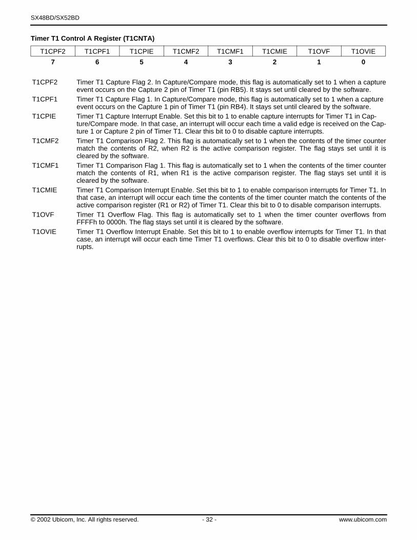
SX48BD/SX52BD
Timer T1 Control A Register (T1CNTA)
T1CPF2 T1CPF1 T1CPIE T1CMF2 T1CMF1 T1CMIE T1OVF T1OVIE
7 6 5 4 3 2 1 0
T1CPF2 Timer T1 Capture Flag 2. In Capture/Compare mode, this flag is automatically set to 1 when a captureevent occurs on the Capture 2 pin of Timer T1 (pin RB5). It stays set until cleared by the software.
T1CPF1 Timer T1 Capture Flag 1. In Capture/Compare mode, this flag is automatically set to 1 when a capture event occurs on the Capture 1 pin of Timer T1 (pin RB4). It stays set until cleared by the software.
T1CPIE Timer T1 Capture Interrupt Enable. Set this bit to 1 to enable capture interrupts for Timer T1 in Cap-ture/Compare mode. In that case, an interrupt will occur each time a valid edge is received on the Cap-ture 1 or Capture 2 pin of Timer T1. Clear this bit to 0 to disable capture interrupts.
T1CMF2 Timer T1 Comparison Flag 2. This flag is automatically set to 1 when the contents of the timer countermatch the contents of R2, when R2 is the active comparison register. The flag stays set until it iscleared by the software.
T1CMF1 Timer T1 Comparison Flag 1. This flag is automatically set to 1 when the contents of the timer countermatch the contents of R1, when R1 is the active comparison register. The flag stays set until it iscleared by the software.
T1CMIE Timer T1 Comparison Interrupt Enable. Set this bit to 1 to enable comparison interrupts for Timer T1. Inthat case, an interrupt will occur each time the contents of the timer counter match the contents of theactive comparison register (R1 or R2) of Timer T1. Clear this bit to 0 to disable comparison interrupts.
T1OVF Timer T1 Overflow Flag. This flag is automatically set to 1 when the timer counter overflows fromFFFFh to 0000h. The flag stays set until it is cleared by the software.
T1OVIE Timer T1 Overflow Interrupt Enable. Set this bit to 1 to enable overflow interrupts for Timer T1. In thatcase, an interrupt will occur each time Timer T1 overflows. Clear this bit to 0 to disable overflow inter-rupts.
© 2002 Ubicom, Inc. All rights reserved. - 32 - www.ubicom.com

SX48BD/SX52BD
Timer T1 Control B Register (T1CNTB)
RTCCOV T1CPEDG T1EXEDG T1PS2-T1PS0 T1MC1-T1MC0
7 6 5 4 3 2 1 0
RTCCOV RTCC Overflow Flag. This flag is automatically set to 1 when the Real-Time Clock/Counter (RTCC)overflows from FFh to 00h. This flag stays set until it is cleared by the software. Note that this flag is notrelated to multi-function timers T1 and T2.
T1CPEDG Timer T1 Capture Edge. This bit sets the edge sensitivity of the Timer T1 input capture pins, Capture 1and Capture 2 (RB4 and RB5). Set this bit to 1 to sense positive-going (low-to-high) edges. Clear thisbit to 0 to sense negative-going (high-to-low) edges.
T1EXEDG Timer T1 External Event Clock Edge. This bit sets the edge sensitivity of the Timer T1 input used tocount external events (RB7). Set this bit to 1 to sense positive-going (low-to-high) edges. Clear this bitto 0 to sense negative-going (high-to-low) edges.
T1PS2-T1PS0
Timer T1 Prescaler Divider field. This 3-bit field specifies the divide-by factor for generating the timerclock from the on-chip system clock: 000 = divide by 1001 = divide by 2010 = divide by 4011 = divide by 8100 = divide by 16101= divide by 32110 = divide by 64111 = divide by 128
For example, setting this field to 010 sets the divide-by factor to 4, which means that the T1 counterregister is incremented once every four system clock cycles.
T1MC1-T1MC0
Timer T1 Mode Control field. This 2-bit field specifies the Timer T1 operating mode as follows:
00 = Software Timer mode01 = PWM mode10 = Capture/Compare mode11 = External Event mode
© 2002 Ubicom, Inc. All rights reserved. - 33 - www.ubicom.com

SX48BD/SX52BD
Timer T2 Control A Register (T2CNTA)
T2CPF2 T2CPF1 T2CPIE T2CMF2 T2CMF1 T2CMIE T2OVF T2OVIE
7 6 5 4 3 2 1 0
T2CPF2 Timer T2 Capture Flag 2. In Capture/Compare mode, this flag is automatically set to 1 when a captureevent occurs on the Capture 2 pin of Timer T2 (pin RC1). It stays set until cleared by the software.
T2CPF1 Timer T2 Capture Flag 1. In Capture/Compare mode, this flag is automatically set to 1 when a capture event occurs on the Capture 1 pin of Timer T2 (pin RC1). It stays set until cleared by the software.
T2CPIE Timer T2 Capture Interrupt Enable. Set this bit to 1 to enable capture interrupts for Timer T2 in Cap-ture/Compare mode. In that case, an interrupt will occur each time a valid edge is received on the Cap-ture 1 or Capture 2 pin of Timer T2. Clear this bit to 0 to disable capture interrupts.
T2CMF2 Timer T2 Comparison Flag 2. This flag is automatically set to 1 when the contents of the timer countermatch the contents of R2, when R2 is the active comparison register. The flag stays set until it iscleared by the software.
T2CMF1 Timer T2 Comparison Flag 1. This flag is automatically set to 1 when the contents of the timer countermatch the contents of R1, when R1 is the active comparison register. The flag stays set until it iscleared by the software.
T2CMIE Timer T2 Comparison Interrupt Enable. Set this bit to 1 to enable comparison interrupts for Timer T2. Inthat case, an interrupt will occur each time the contents of the timer counter match the contents of theactive comparison register (R1 or R2) of Timer T2. Clear this bit to 0 to disable comparison interrupts.
T2OVF Timer T2 Overflow Flag. This flag is automatically set to 1 when the timer counter overflows fromFFFFh to 0000h. The flag stays set until it is cleared by the software.
T2OVIE Timer T2 Overflow Interrupt Enable. Set this bit to 1 to enable overflow interrupts for Timer T2. In thatcase, an interrupt will occur each time Timer T2 overflows. Clear this bit to 0 to disable overflow inter-rupts.
© 2002 Ubicom, Inc. All rights reserved. - 34 - www.ubicom.com
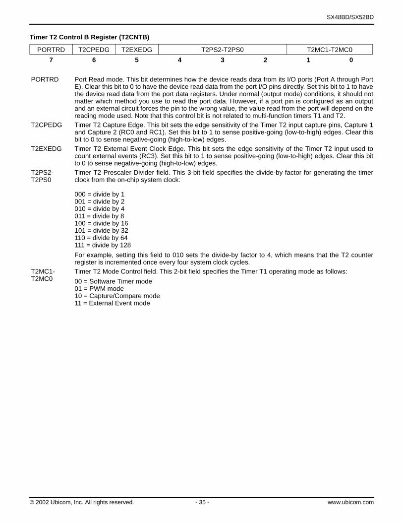
SX48BD/SX52BD
Timer T2 Control B Register (T2CNTB)
PORTRD T2CPEDG T2EXEDG T2PS2-T2PS0 T2MC1-T2MC0
7 6 5 4 3 2 1 0
PORTRD Port Read mode. This bit determines how the device reads data from its I/O ports (Port A through PortE). Clear this bit to 0 to have the device read data from the port I/O pins directly. Set this bit to 1 to havethe device read data from the port data registers. Under normal (output mode) conditions, it should notmatter which method you use to read the port data. However, if a port pin is configured as an outputand an external circuit forces the pin to the wrong value, the value read from the port will depend on thereading mode used. Note that this control bit is not related to multi-function timers T1 and T2.
T2CPEDG Timer T2 Capture Edge. This bit sets the edge sensitivity of the Timer T2 input capture pins, Capture 1and Capture 2 (RC0 and RC1). Set this bit to 1 to sense positive-going (low-to-high) edges. Clear thisbit to 0 to sense negative-going (high-to-low) edges.
T2EXEDG Timer T2 External Event Clock Edge. This bit sets the edge sensitivity of the Timer T2 input used tocount external events (RC3). Set this bit to 1 to sense positive-going (low-to-high) edges. Clear this bitto 0 to sense negative-going (high-to-low) edges.
T2PS2-T2PS0
Timer T2 Prescaler Divider field. This 3-bit field specifies the divide-by factor for generating the timerclock from the on-chip system clock:
000 = divide by 1001 = divide by 2010 = divide by 4011 = divide by 8100 = divide by 16101 = divide by 32110 = divide by 64111 = divide by 128
For example, setting this field to 010 sets the divide-by factor to 4, which means that the T2 counterregister is incremented once every four system clock cycles.
T2MC1-T2MC0
Timer T2 Mode Control field. This 2-bit field specifies the Timer T1 operating mode as follows:
00 = Software Timer mode01 = PWM mode10 = Capture/Compare mode11 = External Event mode
© 2002 Ubicom, Inc. All rights reserved. - 35 - www.ubicom.com

SX48BD/SX52BD
11.0 COMPARATORThe device contains an on-chip differential comparator.Ports RB0-RB2 support the comparator. Pins RB1 andRB2 are the comparator negative and positive inputs,respectively, while RB0 serves as the comparator outputpin. To use these pins in conjunction with the comparator,the user program must configure RB1 and RB2 as inputsand RB0 as an output. The CMP_B register is used toenable the comparator, to read the output of the compar-ator internally, and to enable the output of the comparatorto the comparator output pin.
The comparator enable bits are set to “1” upon reset,thus disabling the comparator. To avoid drawing addi-tional current during the power down mode, the compara-tor should be disabled before entering the power downmode. Here is an example of how to set up the compara-tor and read the CMP_B register.
The final “mov” instruction in this example performs anexchange of data between the working register (W) andthe CMP_B register. This exchange occurs only withaccesses to CMP_B and WKPEND_B. Otherwise, the“mov” instruction does not perform an exchange, but onlymoves data from the source to the destination.
The following figure shows the format of the CMP_B reg-ister.
CMP_B - Comparator Enable/Status Register
;enable RB0 as output
mov
mov
W,#$18
M,W
;set MODE register to access;CMP_B
mov W,#$00 ;clear W
mov !RB,W ;enable comparator and its ;output
... ;delay after enabling ;comparator for response
mov
mov
W,#$18
M,W
;set MODE register to access;CMP_B
mov W,#$00 ;clear W
mov !RB,W ;enable comparator and its ;output and also read CMP_B;(exchange W and CMP_B)
and W,#$01 ;set/clear Z flag based on ;comparator result
snb $03.2 ;test Z flag in STATUS reg ;(0 => RB2<RB1)
jmp rb2_hi ;jump only if RB2>RB1
...
CMP_EN CMP_OE Reserved CMP_RES
Bit 7 Bit 6 Bits 5–1 Bit 0
CMP_EN When cleared to 0, enables the compar-ator.
CMP_OE When cleared to 0, enables the compar-ator output to the RB0 pin if RB0 is con-figured as an output.
CMP_RES Comparator result (Read Only): 1 for RB2>RB1 or 0 for RB2<RB1. Compara-tor must be enabled (CMP_EN = 0) to read the result. The result can be read whether or not the CMP_OE bit is cleared.
© 2002 Ubicom, Inc. All rights reserved. - 36 - www.ubicom.com

SX48BD/SX52BD
Figure 11-1. Comparator Block Diagram
W
MODE
CMP_EN
CMP_OE
RESERVED
CMP_RES
RB0
RB1
RB2
CMP_B
MODE = 08/18
Point to CMP_B
Internal Data Bus
7
6
0
-
+
© 2002 Ubicom, Inc. All rights reserved. - 37 - www.ubicom.com

SX48BD/SX52BD
12.0 RESETPower-On-Reset, Brown-Out reset, watchdog reset,wakeup reset, or external reset initializes the device.Each one of these reset conditions causes the programcounter to branch to the top of the program memory(FFFh).
The device incorporates an on-chip Power-On Reset(POR) circuit that generates an internal reset as Vdd risesduring power-up. Figure 12-1 shows the block diagram ofthe circuit. The circuit contains a 10-bit Delay ResetTimer (DRT) (2 bits contained in the FUSEX register) anda reset latch. The DRT controls the reset timeout delay.The reset latch controls the internal reset signal. Uponpower-up, the reset latch is set (device held in reset), andthe DRT starts counting once it detects a valid logic highsignal at the MCLR pin. Once DRT reaches the end ofthe timeout period (default of 18 msec), the reset latch iscleared, releasing the device from reset state.
Figure 12-2 shows a power-up sequence where MCLR isnot tied to the Vdd pin and Vdd signal is allowed to riseand stabilize before MCLR pin is brought high. Thedevice will actually come out of reset Tdrt msec afterMCLR goes high.
The brown-out circuitry resets the chip when devicepower (Vdd) dips below its minimum allowed value, butnot to zero, and then recovers to the normal value.
Figure 12-3 shows the on-chip Power-On Resetsequence where the MCLR and Vdd pins are tiedtogether. The Vdd signal is stable before the DRT time-out period expires. In this case, the device will receive aproper reset. However, Figure 12-4 depicts a situationwhere Vdd rises too slowly. In this scenario, the DRT willtime-out prior to Vdd reaching a valid operating voltagelevel (Vdd min). This means the device will come out ofreset and start operating with the supply voltage not at avalid level. In this situation, it is recommended that youuse the external RC circuit. The RC delay should exceedthe time period it takes Vdd to reach a valid operating
Note:Ripple counter is 10 bits for Power on Reset (POR)only.
Figure 12-1. Block Diagram of On-Chip Reset Circuit
POR
BROWN-OUT
MIWU
MCLR wdt_time_out
10-Bit AsynchRipple
Counter(DRT Start-Up
Timer)
Vdd
rc_clkdrt_time
_out
S
R
Q
QNRESET
POR
enable
Figure 12-2. Time-Out Sequence on Power-Up (MCLR not tied to Vdd)
Figure 12-3. Time-out Sequence on Power-up(MCLR tied to Vdd): Slow Rise Time
Figure 12-4. External Power-On Reset Circuit (For Slow Vdd Power-up)
Figure 12-5. Time-out Sequence on Power-up (MCLR tied to Vdd): Fast Vdd Rise Time
Vdd
MCLR
POR
drt_time_out
RESET
Tdrt
Vdd
MCLR
POR
drt_time_out
RESET
Tdrt
V1
Vdd
R
C
MCLR
DR1
Vdd
MCLR
POR
drt_time_out
RESET
Tdrt
© 2002 Ubicom, Inc. All rights reserved. - 38 - www.ubicom.com
SX48BD/SX52BD
A 2-bit field in the FUSEX register can be used to specify the Delay Reset Timer (DRT) timeout period that results in an automatic wake-up from the power down mode.
10 = 0.25 msec11 = 18 msec (default)00 = 60 msec01 = 1 secFor fast start-up from the power down mode, clear the SLEEPCLK bit and set the WDRT1:WDRT0 field to 00. This will keep the clock operating during the power down mode and allow a minimum start-up delay.
Note 1: The external Power-On Reset circuit is requiredonly if Vdd power-up is too slow. The diode D helps dis-charge the capacitor quickly when Vdd powers down andcomes back within a short period of time.
Note 2: R < 40 kΩ is recommended to make sure thatvoltage drop across R does not violate the device electri-cal specifications.
R1 = 100Ω to 1kΩ will limit any current flowing into MCLRfrom external capacitor C. This helps prevent MCLR pinbreakdown due to Electrostatic Discharge (ESD) or Elec-trical Overstress (EOS).
13.0 BROWN-OUT DETECTORThe on-chip brown-out detection circuitry resets thedevice when Vdd dips below the specified brown-out volt-age. The device is held in reset as long as Vdd staysbelow the brown-out voltage. The device will come out ofreset when Vdd rises above the brown-out voltage. Thebrown-out level can be set to 2.2V, 2.4V, OR 4.1V levelsthrough BOR1:BOR0 bits in the FUSEX register.
© 2002 Ubicom, Inc. All rights reserved. - 39 - www.ubicom.com
SX48BD/SX52BD
14.0 REGISTER STATES UPON DIFFERENT RESET CONDITIONSThe effect of different reset operations on a registerdepends on the register and the type of reset operation.Some registers are initialized to specific values, someare left unchanged, some are undefined, and some areinitialized to an unknown value.
A register that starts with an unknown value should beinitialized by the software to a known value; you cannotsimply test the initial state and rely on it starting in that
state consistently. Table 14-1 lists the SX registers andshows the state of each register upon reset, with a differ-ent column for each type of reset.
Table 14-1. Register States Upon Different Resets
Register Power-On Wakeup Brown-out Watchdog Timeout MCLR
W Undefined Unchanged Undefined Unchanged Unchanged
OPTION FFh FFh FFh FFh FFh
MODE (Note 3) 1Fh 1Fh 1Fh 1Fh 1Fh
RTCC (01h) Undefined Unchanged Undefined Unchanged Unchanged
PC (02h) FFh FFh FFh FFh FFh
STATUS (03h)(Note 3)
Bits 0-2: Unde-finedBits 3-4: 11Bits 5-7: 000
Bits 0-2: Un-changedBits 3-4: Unch.Bits 5-7: 000
Bits 0-4: Unde-finedBits 5-7: 000
Bits 0-2: Un-changedBits 3-4: (Note 1)Bits 5-7: 000
Bits 0-2: Un-changedBits 3-4: (Note 2)Bits 5-7:000
FSR (04h) Undefined Bits 0-6: Un-changedBit 7: 1
Bits 0-6: Unde-finedBit 7: 1
Bits 0-6: Un-changedBit 7: 1
Bits 0-6: Un-changedBit 7: 1
RA through REDirection
FFh FFh FFh FFh FFh
RA through RE Data Undefined Unchanged Undefined Unchanged Unchanged
Other File Registers -SRAM
Undefined Unchanged Undefined Unchanged Unchanged
CMP_B Bits 0, 6-7: 1Bits 1-5: Unde-fined
Bits 0, 6-7: 1Bits 1-5: Undefined
Bits 0, 6-7: 1Bits 1-5: Unde-fined
Bits 0, 6-7: 1Bits 1-5: Undefined
Bits 0, 6-7: 1Bits 1-5: Undefined
WKPND_B Undefined Unchanged Undefined Unchanged Unchanged
WKED_B FFh FFh FFh FFh FFh
WKEN_B FFh FFh FFh FFh FFh
ST_B through ST_E FFh FFh FFh FFh FFh
LVL_A through LVL_E FFh FFh FFh FFh FFh
PLP_A through PLP_E FFh FFh FFh FFh FFh
Watchdog Counter Undefined Unchanged Undefined Unchanged Unchanged
Timers T1 and T2 Free-Running Timer/Counter
0001 0001 0001 0001 0001
Timers T1 and T2 Com-pare/Capture Registers
0000 0000 0000 0000 0000
Timers T1 and T2 Control Registers (Note 3)
00 00 00 00 00
NOTE: 1. Watchdog reset during power down mode: 00 (bits TO, PD) Watchdog reset during Active mode: 01 (bits TO, PD)
NOTE: 2. External reset during power down mode: 10 (bits TO, PD) External reset during Active mode: Unchanged (bits TO, PD)
Note:. 3. MODE, STATUS, and Timer registers are not initialized properly by the development system in Debug mode.
© 2002 Ubicom, Inc. All rights reserved. - 40 - www.ubicom.com

SX48BD/SX52BD
15.0 INSTRUCTION SETAs mentioned earlier, the SX family of devices uses amodified Harvard architecture with memory-mappedinput/output. The device also has a RISC type architec-ture in that there are 43 single-word basic instructions.The instruction set contains byte-oriented file register, bit-oriented file register, and literal/control instructions.
Working register W is one of the CPU registers, whichserves as a pseudo accumulator. It is a pseudo accumu-lator in a sense that it holds the second operand,receives the literal in the immediate type instructions, andalso can be program-selected as the destination register.The bank of 31 file registers can also serve as the pri-mary accumulators, but they represent the first operandand may be program-selected as the destination regis-ters.
15.1 Instruction Set Features1. All single-word (12-bit) instructions for compact code
efficiency.2. All instructions are single cycle except the jump type in-
structions (JMP, CALL) and failed test instructions (DECSZ fr, INCSZ fr, SB bit, SNB bit), which are two-cycle.
3. A set of file registers can be addressed directly or indi-rectly, and serve as accumulators to provide first oper-and; W register provides the second operand.
4. Many instructions include a destination bit which se-lects either the register file or the accumulator as the destination for the result.
5. Bit manipulation instructions (Set, Clear, Test and Skip if Set, Test and Skip if Clear).
6. STATUS Word register memory-mapped as a register file, allowing testing of status bits (carry, digit carry, ze-ro, power down, and timeout).
7. Program Counter (PC) memory-mapped as register file allows W to be used as offset register for indirect ad-dressing of program memory.
8. Indirect addressing data pointer FSR (file select regis-ter) memory-mapped as a register file.
9. IREAD instruction allows reading the instruction from the program memory addressed by W and upper four bits of MODE register.
10.Eight-level, 12-bit push/pop hardware stack for sub-routine linkage using the Call and Return instructions.
11.Seven addressing mode provide great flexibility.
15.2 Instruction ExecutionAn instruction goes through a four-stage pipeline to beexecuted (Figure 15-1). The first instruction is fetchedfrom the program memory on the first clock cycle. On thesecond clock cycle, the first instruction is decoded andthe second instruction is fetched. On the third clock cycle,the first instruction is executed, the second instruction isdecoded, and the third instruction is fetched. On thefourth clock cycle, the first instruction’s results are writtento its destination, the second instruction is executed, thethird instruction is decoded, and the fourth instruction isfetched. Once the pipeline is full, instructions are exe-cuted at the rate of one per clock cycle.
Instructions that directly affect the contents of the pro-gram counter (such as jumps and calls) require that thepipeline be cleared and subsequently refilled. Therefore,these instructions take more than one clock cycle.
The instruction execution time is derived by dividing theoscillator frequency by one (bit 11 of the FUSE Word reg-ister must be initialized to 0).
Figure 15-1. Pipeline and Clock Scheme
Fetch Decode Execute Write
Clock
Cycle
1
Clock
Cycle
2
Clock
Cycle
3
Clock
Cycle
4
© 2002 Ubicom, Inc. All rights reserved. - 41 - www.ubicom.com
SX48BD/SX52BD
15.3 Addressing ModesThe device support the following addressing modes:
Data DirectData IndirectData SemidirectImmediateProgram DirectProgram IndirectRelative
Both direct and indirect addressing modes are available.The INDF register, though physically not implemented, isused in conjunction with the indirect data pointer (FSR) toperform indirect addressing. An instruction using INDF asits operand field actually performs the operation on theregister pointed by the contents of the FSR. Conse-quently, processing two multiple-byte operands requiresalternate loading of the operand addresses into the FSRpointer as the multiple byte data fields are processed.
Examples:
Direct addressing:
Indirect Addressing:
Semidirect Addressing:
15.4 The Bank InstructionOften it is desirable to set the bank select bits of the FSRregister in one instruction cycle. The Bank instructionprovides this capability. This instruction sets the upper 3bits 4, 5 and 6 of the FSR to point to a specific RAM bankwithout affecting the lower 4 FSR bits, in preparation forusing direct or semidirect addressing. Bit 7 of the FSRregister is used to select the lower or upper block ofbanks.
Example:
15.5 Bit ManipulationThe instruction set contains instructions to set, reset, andtest individual bits in data memory. The device is capableof bit addressing anywhere in data memory.
15.6 Input/Output OperationThe device contains three registers associated with eachI/O port. The first register (Data Direction Register), con-
figures each port pin as a Hi-Z input or output. The sec-ond register (TTL/CMOS Register), selects the desiredinput level for the input. The third register (Pull-Up Regis-ter), enables a weak pull-up resistor on the pin configuredas a input. To read or write these registers, you must firstwrite an appropriate value into the MODE register toselect the desired register set, and then use the “mov!rx,W” instruction to read or write the register.
15.6.1 Read-Modify-Write Considerations
When two successive instructions are used on the sameI/O port (except “mov Rx, W”) with a very high clock rate,the “write” part of one instruction might not occur soonenough before the “read” part of the very next instruction,resulting in getting “old” data for the second instruction.To ensure predictable results, avoid using two successiveread-modify-write instructions that access the same portdata register if the clock rate is high or, insert 3 NOPinstructions between the successive read-modify-writeinstructions (if SYNC bit in the FUSE register is enabled,5 NOP instructions are required). For operating frequen-cies of 50 Mhz or lower, if bit 7 of the T2CNTB (PORTRD)is set, the port reads data from the data register insteadof port pins. In this case, the NOP instructions are notrequired.
In the default device configuration, when a read is per-formed from a port bit position, the operation is actuallyreading the voltage level on the pin itself, not necessarilythe bit value stored in the port data register. This is truewhether the pin is configured to operate as an input or anoutput. Therefore, with the pin configured to operate asan input, the data register contents have no effect on thevalue that you read. With the pin configured to operate asan output, what is read generally matches what has beenwritten to the register. PORTRD of the T2CNTB registerdetermines how the device reads data from its I/O ports(Port A through Port E). Clear this bit to 0 to have thedevice read data from the port I/O pins directly. Set thisbit to 1 to have the device read data from the port dataregisters. Under normal output mode conditions, it shouldnot matter which method you use to read the port data.However, if a port pin is configured as an output and anexternal circuit forces the pin to the opposite value, thevalue read from the port will depend on the reading modeused. Note that this control bit is not related to multi-func-tion timers T1 and T2.
15.7 Increment/DecrementThe current selected bank of 31 registers serves as a setof accumulators. The instruction set contains instructionsto increment and decrement the register file. The devicealso includes both INCSZ fr (increment file register andskip if zero) and DECSZ fr (decrement file register andskip if zero) instructions.
15.8 Loop Counting and Data Pointing Testing
The device has specific instructions to facilitate loopcounting. The DECSZ fr (decrement file register and skipif zero) tests any one of the file registers and skips thenext instruction (which can be a branch back to loop) ifthe result is zero.
mov W,#1
mov RA,W ;move “1” to RA
mov W,#RA
mov FSR,W ;FSR = address of RA
mov INDF,#$01 ;move “1” to RA
mov W,#$00
mov FSR,W ;FSR = bank 0 address
inc $1F ;increment file ;register 0Fh
bank $E0 ;Select Bank E in FSR
inc $1F ;increment file register;EFh using semidirect addressing
© 2002 Ubicom, Inc. All rights reserved. - 42 - www.ubicom.com

SX48BD/SX52BD
15.9 Branch and Loop Call InstructionsThe device contains an 8-level hardware stack where thereturn address is stored with a subroutine call. Multiplestack levels allow subroutine nesting. The instruction setsupports absolute address branching.
15.9.1 Jump Operation
When a JMP instruction is executed, the lower nine bitsof the program counter are loaded with the address of thespecified label. The upper three bits of the programcounter are loaded with the page select bits, PA2:PA0,contained in the STATUS register. Therefore, care mustbe exercised to ensure the page select bits are pointingto the correct page before the jump occurs.
15.9.2 Page Jump Operation
When a JMP instruction is executed and the intendeddestination is on a different page, the page select bitsmust be initialized with appropriate values to point to thedesired page before the jump occurs. This can be doneeasily with SETB and CLRB instructions or by writing avalue to the STATUS register. The device also has thePAGE instruction, which automatically selects the page ina single-cycle execution.
Note:“N” must be 0, 1, 2, or 3.
15.9.3 Call Operation
The following happens when a CALL instruction is exe-cuted:
• The current value of the program counter is increment-ed and pushed onto the top of the stack.
• The lower eight bits of the label address are copied into the lower eight bits of the program counter.
• The ninth bit of the Program Counter is cleared to zero. • The page select bits (in STATUS register) are copied
into the upper three bits of the 12-bit program counter. This means that the call destination must start in thelower half of any page. For example, 00h-0FFh, 200h-2FFh, 400h-4FFh, etc.
15.9.4 Page Call Operation
When a subroutine that resides on a different page iscalled, the page select bits must contain the proper val-ues to point to the desired page before the call instructionis executed. This can be done easily using SETB andCLRB instructions or writing a value to the STATUS reg-ister. The device also has the PAGE instruction, whichautomatically selects the page in a single-cycle execu-tion.
15.10 Return InstructionsThe device has several instructions for returning fromsubroutines and interrupt service routines. The returnfrom subroutine instructions are RET (return withoutaffecting W), RETP (same as RET but affects PA2:PA0),RETI (return from interrupt), RETIW (return and add W toRTCC), and RETW #literal (return and place literal in W).The literal serves as an immediate data value from mem-ory. This instruction can be used for table lookup opera-tions. To do table lookup, the table must contain a stringof RETW #literal instructions. The first instruction just infront of the table calculates the offset into the table. Thetable can be used as a result of a CALL.
STATUS<7:5> JMP LABEL (9 BITS)
PC<11:9> PC<8:0>
PAGE N
STATUS<7:5> JMP LABEL (9 BITS)
PC<11:9> PC<8:0>
STATUS<7:5> 0 CALL LABEL (8 BITS)
PC<11:9> PC<8> PC<7:0>
PAGE N
STATUS<7:5> 0 CALL LABEL (8 BITS)
PC<11:9> PC<8> PC<7:0>
© 2002 Ubicom, Inc. All rights reserved. - 43 - www.ubicom.com
SX48BD/SX52BD
15.11 Subroutine Operation15.11.1 Push Operation
When a subroutine is called, the return address ispushed onto the subroutine stack. Specifically, eachaddress in the stack is moved to the next lower level inorder to make room for the new address to be stored.Stack 1 receives the contents of the program counter.Stack 8 is overwritten with what was in Stack 7. The con-tents of stack 8 are lost.
15.11.2 Pop Operation
When a return instruction is executed the subroutinestack is popped. Specifically, the contents of Stack 1 arecopied into the program counter and the contents of eachstack level are moved to the next higher level. For exam-ple, Stack 1 receives the contents of Stack 2, etc., untilStack 7 is overwritten with the contents of Stack 8. Stack8 is left unchanged, so the contents of Stack 8 are dupli-cated in Stack 7.
PC<11:0>
STACK 1
STACK 2
STACK 3
STACK 4
STACK 5
STACK 6
STACK 7
STACK 8
PC<11:0>
STACK 1
STACK 2
STACK 3
STACK 4
STACK 5
STACK 6
STACK 7
STACK 8
© 2002 Ubicom, Inc. All rights reserved. - 44 - www.ubicom.com
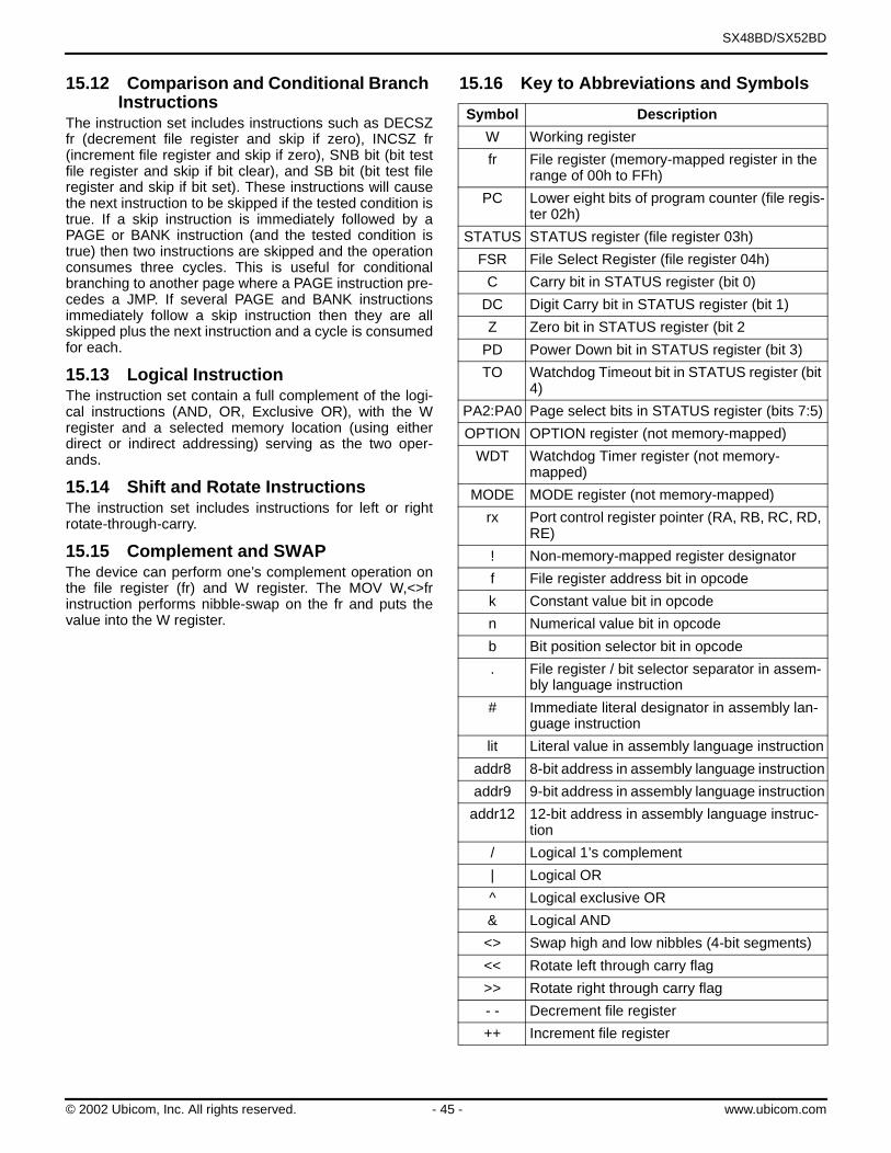
SX48BD/SX52BD
15.12 Comparison and Conditional Branch Instructions
The instruction set includes instructions such as DECSZfr (decrement file register and skip if zero), INCSZ fr(increment file register and skip if zero), SNB bit (bit testfile register and skip if bit clear), and SB bit (bit test fileregister and skip if bit set). These instructions will causethe next instruction to be skipped if the tested condition istrue. If a skip instruction is immediately followed by aPAGE or BANK instruction (and the tested condition istrue) then two instructions are skipped and the operationconsumes three cycles. This is useful for conditionalbranching to another page where a PAGE instruction pre-cedes a JMP. If several PAGE and BANK instructionsimmediately follow a skip instruction then they are allskipped plus the next instruction and a cycle is consumedfor each.
15.13 Logical InstructionThe instruction set contain a full complement of the logi-cal instructions (AND, OR, Exclusive OR), with the Wregister and a selected memory location (using eitherdirect or indirect addressing) serving as the two oper-ands.
15.14 Shift and Rotate InstructionsThe instruction set includes instructions for left or rightrotate-through-carry.
15.15 Complement and SWAPThe device can perform one’s complement operation onthe file register (fr) and W register. The MOV W,<>frinstruction performs nibble-swap on the fr and puts thevalue into the W register.
15.16 Key to Abbreviations and Symbols
Symbol Description
W Working register
fr File register (memory-mapped register in the range of 00h to FFh)
PC Lower eight bits of program counter (file regis-ter 02h)
STATUS STATUS register (file register 03h)
FSR File Select Register (file register 04h)
C Carry bit in STATUS register (bit 0)
DC Digit Carry bit in STATUS register (bit 1)
Z Zero bit in STATUS register (bit 2
PD Power Down bit in STATUS register (bit 3)
TO Watchdog Timeout bit in STATUS register (bit 4)
PA2:PA0 Page select bits in STATUS register (bits 7:5)
OPTION OPTION register (not memory-mapped)
WDT Watchdog Timer register (not memory-mapped)
MODE MODE register (not memory-mapped)
rx Port control register pointer (RA, RB, RC, RD, RE)
! Non-memory-mapped register designator
f File register address bit in opcode
k Constant value bit in opcode
n Numerical value bit in opcode
b Bit position selector bit in opcode
. File register / bit selector separator in assem-bly language instruction
# Immediate literal designator in assembly lan-guage instruction
lit Literal value in assembly language instruction
addr8 8-bit address in assembly language instruction
addr9 9-bit address in assembly language instruction
addr12 12-bit address in assembly language instruc-tion
/ Logical 1’s complement
| Logical OR
^ Logical exclusive OR
& Logical AND
<> Swap high and low nibbles (4-bit segments)
<< Rotate left through carry flag
>> Rotate right through carry flag
- - Decrement file register
++ Increment file register
© 2002 Ubicom, Inc. All rights reserved. - 45 - www.ubicom.com

SX48BD/SX52BD
16.0 INSTRUCTION SET SUMMARY TABLETable 16-1 lists all of the instructions, organized by cate-gory. For each instruction, the table shows the instructionmnemonic (as written in assembly language), a briefdescription of what the instruction does, the number ofinstruction cycles required for execution, the binaryopcode, and the status flags affected by the instruction.
The “Cycles” column typically shows a value of 1, whichmeans that the overall throughput for the instruction isone per clock cycle. In some cases, the exact number of
cycles depends on the outcome of the instruction (suchas the test-and-skip instructions). In those cases, all pos-sible numbers of cycles are shown in the table.
The instruction execution time is derived by dividing theoscillator frequency by one (bit 11 of the FUSE Word reg-ister must be initialized to 0).
Table 16-1. The SX Instruction Set
Mnemonic, Operands Description Cycles Opcode Flags
Affected
Logical Operations
AND fr, W AND of fr and W into fr (fr = fr & W) 1 0001 011f ffff Z
AND W, fr AND of W and fr into W (W = W & fr) 1 0001 010f ffff Z
AND W,#lit AND of W and Literal into W (W = W & lit) 1 1110 kkkk kkkk Z
NOT fr Complement of fr into fr (fr = fr ^ FFh) 1 0010 011f ffff Z
OR fr,W OR of fr and W into fr (fr = fr | W) 1 0001 001f ffff Z
OR W,fr OR of W and fr into fr (W = W | fr) 1 0001 000f ffff Z
OR W,#lit OR of W and Literal into W (W = W | lit) 1 1101 kkkk kkkk Z
XOR fr,W XOR of fr and W into fr (fr = fr ^ W) 1 0001 101f ffff Z
XOR W,fr XOR of W and fr into W (W = W ^ fr) 1 0001 100f ffff Z
XOR W,#lit XOR of W and Literal into W (W = W ^ lit) 1 1111 kkkk kkkk Z
Arithmetic and Shift Operations
ADD fr,W Add W to fr (fr = fr + W); carry flag is added if CF bit in FUSEX register is cleared to 0
1 0001 111f ffff C, DC, Z
ADD W,fr Add fr to W (W = W + fr); carry flag is added if CF bit in FUSEX register is cleared to 0
1 0001 110f ffff C, DC, Z
CLR fr Clear fr (fr = 0) 1 0000 011f ffff Z
CLR W Clear W (W = 0) 1 0000 0100 0000 Z
CLR !WDT Clear Watchdog Timer (TO = 1, PD = 1, clears prescaler if assigned)
1 0000 0000 0100 TO, PD
DEC fr Decrement fr (fr = fr - 1) 1 0000 111f ffff Z
DECSZ fr Decrement fr and Skip if Zero (fr = fr - 1 and skip next instruction if result is zero)
1 or
2 (skip)
0010 111f ffff none
INC fr Increment fr (fr = fr + 1) 1 0010 101f ffff Z
INCSZ fr Increment fr and Skip if Zero (fr = fr + 1 and skip next instruction if result is zero)
1 or
2 (skip)
0011 111f ffff none
RL fr Rotate fr Left through Carry (fr = << fr) 1 0011 011f ffff C
RR fr Rotate fr Right through Carry (fr = >> fr) 1 0011 001f ffff C
SUB fr,W Subtract W from fr (fr = fr - W); complement of the carry flag is subtracted if CF bit in FUSEX register is cleared to 0
1 0000 101f ffff C, DC, Z
SWAP fr Swap High/Low Nibbles of fr (fr = <> fr) 1 0011 101f ffff none
© 2002 Ubicom, Inc. All rights reserved. - 46 - www.ubicom.com

SX48BD/SX52BD
Bitwise Operations
CLRB fr.bit Clear Bit in fr (fr.bit = 0) 1 0100 bbbf ffff none
SB fr.bit Test Bit in fr and Skip if Set (test fr.bit and skip next instruction if bit is 1)
1 or
2 (skip)
0111 bbbf ffff none
SETB fr.bit Set Bit in fr (fr.bit = 1) 1 0101 bbbf ffff none
SNB fr.bit Test Bit in fr and Skip if Clear (test fr.bit and skip next instruction if bit is 0)
1 or
2 (skip)
0110 bbbf ffff none
Data Movement Instructions
MOV fr,W Move W to fr (fr = W) 1 0000 001f ffff none
MOV W,fr Move fr to W (W = fr) 1 0010 000f ffff Z
MOV W,fr-W Move (fr-W) to W (W = fr - W); complement of carry flag is subtracted if CF bit in FUSEX regis-ter is cleared to 0
1 0000 100f ffff C, DC, Z
MOV W,#lit Move Literal to W (W = lit) 1 1100 kkkk kkkk none
MOV W,/fr Move Complement of fr to W (W = fr ^ FFh) 1 0010 010f ffff Z
MOV W,--fr Move (fr-1) to W (W = fr - 1) 1 0000 110f ffff Z
MOV W,++fr Move (fr+1) to W (W = fr + 1) 1 0010 100f ffff Z
MOV W,<<fr Rotate fr Left through Carry and Move to W (W = << fr)
1 0011 010f ffff C
MOV W,>>fr Rotate fr Right through Carry and Move to W(W = >> fr)
1 0011 000f ffff C
MOV W,<>fr Swap High/Low Nibbles of fr and move to W(W = <> fr)
1 0011 100f ffff none
MOV W,M Move MODE Register to W (W = MODE), high nibble of W cleared
1 0000 0100 0010 none
MOVSZ W,--fr Move (fr-1) to W and Skip if Zero (W = fr -1 and skip next instruction if result is zero)
1
2 (skip)
0010 110f ffff none
MOVSZ W,++fr Move (fr+1) to W and Skip if Zero (W = fr + 1 and skip next instruction if result is zero)
1
2 (skip)
0011 110f ffff none
MOV M,W Move W to MODE Register (MODE = W) 1 0000 0100 0011 none
MOV M,#lit Move Literal to MODE Register (MODE = lit, only lower 4 bits)
1 0000 0101 kkkk none
MOV !rx,W Move Data Between W and Control Register:rx = W (move W to rx) - MODE Reg bit 4 = 1W = rx (move rx to W) - MODE Reg bit 4 = 0rx <=> W (exchange W and rx) - MODE = x8 or x9
1 0000 0000 ffff none
MOV !OPTION, W Move W to OPTION Register (OPTION = W) 1 0000 0000 0010 none
TEST fr Test fr for Zero (fr = fr to set or clear Z flag) 1 0010 001f ffff Z
Program Control Instructions
Table 16-1. The SX Instruction Set (Continued)
Mnemonic, Operands Description Cycles Opcode Flags
Affected
© 2002 Ubicom, Inc. All rights reserved. - 47 - www.ubicom.com

SX48BD/SX52BD
CALL addr8 Call Subroutine: top-of-stack = program counter + 1PC(7:0) = addr8program counter (8) = 0program counter (11:9) = PA2:PA0
3 1001 kkkk kkkk none
JMP addr9 Jump to Address:PC(7:0) = addr9(7:0)program counter (8) = addr9(8)program counter (11:9) = PA2:PA0
3 101k kkkk kkkk none
NOP No Operation 1 0000 0000 0000 none
RET Return from Subroutine (program counter = top-of-stack)
Note: Not recommended, use RETP
3 0000 0000 1100 none
RETP Return from Subroutine Across Page Boundary(PA2:PA0 = top-of-stack (11:9) and program counter = top-of-stack)
3 0000 0000 1101 PA2, PA1, PA0
RETI Return from Interrupt (restore W, STATUS, FSR, MODE and program counter from shadow registers)
3 0000 0000 1110 all STATUS except TO, PD bits
RETIW Return from Interrupt and add W to RTCC (re-store W, STATUS, FSR, MODE and program counter from shadow registers; and add W to the RTCC register)
3 0000 0000 1111 all STATUS except TO, PD bits
RETW lit Return from Subroutine with Literal in W (W = lit and program counter = top-of-stack)
3 1000 kkkk kkkk none
System Control Instructions
BANK addr12 Load Bank Number into FSR(6:4)FSR(6:4) = addr12(10:8)
1 0000 0001 1nnn none
IREAD Read Word from Instruction MemoryMODE:W = data at address (MODE:W)
4 0000 0100 0001 none
PAGE addr12 Load Page Number into STATUS(7:5)STATUS(7:5) = addr12(11:9)
1 0000 0001 0nnn PA2, PA1, PA0
SLEEP Power Down ModeWDT = 00h, TO = 1, stop oscillator
(PD = 0, clear prescaler if assigned)
1 0000 0000 0011 TO, PD
Table 16-1. The SX Instruction Set (Continued)
Mnemonic, Operands Description Cycles Opcode Flags
Affected
© 2002 Ubicom, Inc. All rights reserved. - 48 - www.ubicom.com

SX48BD/SX52BD
16.1 Equivalent Assembler MnemonicsSome assemblers support additional instruction mne-monics that are special cases of existing instructions oralternative mnemonics for standard ones. For example,an assembler might support the mnemonic “CLC” (clearcarry), which is interpreted the same as the instruction
“clrb $03.0” (clear bit 0 in the STATUS register). Some ofthe commonly supported equivalent assembler mnemon-ics are described in Table 16-2.
Table 16-2. Equivalent Assembler Mnemonics
Syntax Description Equivalent Cycles
CLC Clear Carry Flag CLRB $03.0 1
CLZ Clear Zero Flag CLRB $03.2 1
JMP W Jump Indirect W MOV $02,W 3
JMP PC+W Jump Indirect W Relative ADD $02,W 3
MODE imm4 Move Immediate to MODE Register
MOV M,#lit 1
NOT W Complement W XOR W,#$FF 1
SC Skip if Carry Flag Set SB $03.0 1 or 2 (note 1)
SKIP Skip Next Instruction SNB $02.0 or SB $02.0 2 (note 2)
Note 1: The SC instruction takes 1 cycle if the tested condition is false or 2 cycles if the tested condition is true.
Note 2: The assembler converts the SKIP instruction into a SNB or SB instruction that tests the least significant bitof the program counter, choosing SNB or SB so that the tested condition is always true.
© 2002 Ubicom, Inc. All rights reserved. - 49 - www.ubicom.com

SX48BD/SX52BD
17.0 ELECTRICAL CHARACTERISTICS
17.1 Absolute Maximum Ratings (beyond which permanent damage may occur)
Ambient temperature under bias -40°C to +85°C
Storage temperature -65°C to +150°C
Voltage on Vdd with respect to Vss 0 V to +7.0 V
Voltage on OSC1 with respect to Vss 0 V to +13.5 V
Voltage on MCLR with respect to Vss 0 V to +13.5 V
Voltage on all other pins with respect to Vss - 0.6 V to (Vdd + 0.6 V) V
Total power dissipation 1 W at 70°C
1.5 W at 25°C
Max. current out of Vss pins 180 mA at 70°C
300 mA at 25°C
Max. current into Vdd pins 180 mA at 70°C
300 mA at 25°C
Max. DC current into an input pin (with internal protection diode forward biased)
+500 µA
Input clamp current, Iik (Vi < 0 or Vi > Vdd) +20 mA
Output clamp current, lok (VO < 0 or VO > Vdd) +20 mA
Max. allowable sink current per I/O pin 45 mA
Max. allowable source current per I/O pin 45 mA
Max. allowable sink current per group of I/O pins between Vdd pins 50 mA
Max. allowable source current per group of I/O pins between Vdd pins 50 mA
Latchup 200 mA
θJA, 48-pin Package 85°C/W
θJA, 52-pin Package 82°C/W
Number of EEPROM Write Cycles 10,000
ESD Human Body Model - all pins 2000V
ESD Machine Model - all pins 200V
© 2002 Ubicom, Inc. All rights reserved. - 50 - www.ubicom.com
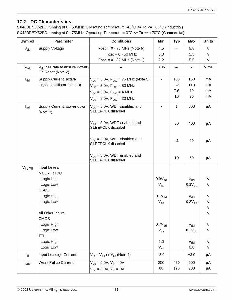
SX48BD/SX52BD
17.2 DC CharacteristicsSX48BD/SX52BD running at 0 - 50MHz: Operating Temperature -40°C <= Ta <= +85°C (Industrial)
SX48BD/SX52BD running at 0 - 75MHz: Operating Temperature 0°C <= Ta <= +70°C (Commercial)
Symbol Parameter Conditions Min Typ Max Units
Vdd Supply Voltage Fosc = 0 - 75 MHz (Note 5)
Fosc = 0 - 50 MHz
Fosc = 0 - 32 MHz (Note 1)
4.5
3.0
2.2
– 5.5
5.5
5.5
V
V
V
SVdd Vdd rise rate to ensure Power-On Reset (Note 2)
– 0.05 – - V/ms
Idd Supply Current, active
Crystal oscillator (Note 3)
Vdd = 5.0V, Fosc = 75 MHz (Note 5)
Vdd = 5.0V, Fosc = 50 MHz
Vdd = 5.0V, Fosc = 4 MHz
Vdd = 3.0V, Fosc = 20 MHz
- 106
82
7.6
16
150
110
10
20
mA
mA
mA
mA
Ipd Supply Current, power down
(Note 3)
Vdd = 5.0V, WDT disabled and SLEEPCLK disabled
Vdd = 5.0V, WDT enabled and SLEEPCLK disabled
Vdd = 3.0V, WDT disabled and SLEEPCLK disabled
Vdd = 3.0V, WDT enabled and SLEEPCLK disabled
- 1
50
<1
10
300
400
20
50
µA
µA
µA
µA
Vih, Vil Input Levels
MCLR, RTCC
Logic High
Logic Low
OSC1
Logic High
Logic Low
All Other Inputs
CMOS
Logic High
Logic Low
TTL
Logic High
Logic Low
0.9Vdd
Vss
0.7Vdd
Vss
0.7Vdd
Vss
2.0
Vss
Vdd
0.1Vdd
Vdd
0.3Vdd
Vdd
0.3Vdd
Vdd
0.8
V
V
V
V
V
V
V
V
V
V
Iil Input Leakage Current Vin = Vdd or Vss (Note 4) -3.0 +3.0 µA
Ipup Weak Pullup Current Vdd = 5.5V, Vin = 0V
Vdd = 3.0V, Vin = 0V
250
80
430
120
600
200
µA
µA
© 2002 Ubicom, Inc. All rights reserved. - 51 - www.ubicom.com
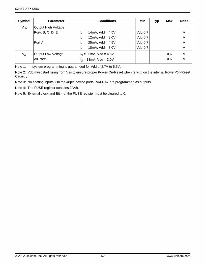
SX48BD/SX52BD
Note 1: In- system programming is guaranteed for Vdd of 2.7V to 5.5V.
Note 2: Vdd must start rising from Vss to ensure proper Power-On-Reset when relying on the internal Power-On-ResetCircuitry.
Note 3: No floating inputs. On the 48pin device ports RA4-RA7 are programmed as outputs.
Note 4: The FUSE register contains 0AAh.
Note 5: External clock and Bit 4 of the FUSE register must be cleared to 0.
Voh Output High Voltage
Ports B, C, D, E
Port A
Ioh = 14mA, Vdd = 4.5V
Ioh = 12mA, Vdd = 3.0V
Ioh = 25mA, Vdd = 4.5V
Ioh = 18mA, Vdd = 3.0V
Vdd-0.7
Vdd-0.7
Vdd-0.7
Vdd-0.7
V
V
V
V
Vol Output Low Voltage
All Ports
Iol = 25mA, Vdd = 4.5V
Iol = 18mA, Vdd = 3.0V
0.6
0.6
V
V
Symbol Parameter Conditions Min Typ Max Units
© 2002 Ubicom, Inc. All rights reserved. - 52 - www.ubicom.com

SX48BD/SX52BD
17.3 AC CharacteristicsSX48BD/SX52BD running at 50MHz: Operating Temperature -40°C <= Ta <= +85°C (Industrial)
SX48BD/SX52BD running at 75MHz: Operating Temperature 0°C <= Ta <= +70°C (Commercial)
Note:Data in the Typical (“TYP”) column is at 5V, 25°C unless otherwise stated.
Symbol Parameter Min Typ Max Units Conditions
Fosc External CLKIN Frequency DC - 32.0
1.0
4.0
1.0
8.0
50.0
75.0
KHz
MHz
MHz
MHz
MHz
MHz
MHz
LP1
LP2
RC
XT1
XT2
HS1/HS2/HS3
HS3
Oscillator Frequency
(Crystal/Resonator)
DC
0.032
DC
0.032
1.0
1.0
1.0
- 32.0
1.0
4.0
1.0
8.0
50.0
75.0
KHz
MHz
MHz
MHz
MHz
MHz
MHz
LP1
LP2
RC
XT1
XT2
HS1/HS2/HS3
HS3
Tosc External CLKIN Period 31.25
1.0
250.0
1.0
125.0
20.0
13.3
- - µs
µs
ns
µs
ns
ns
ns
LP1
LP2
RC
XT1
XT2
HS1/HS2/HS3
HS3
Oscillator Period
(Crystal/Resonator)
31.25
1.0
250.0
1.0
125.0
20.0
13.3
- -
31.25
-
31.25
1000
1000
-
µs
µs
ns
µs
ns
ns
LP1
LP2
RC
XT1
XT2
HS1/HS2/HS3
HS3
TosL, TosH Clock in (OSC1) Low or High Time 400
50.0
8.0
5.3
- - ns
ns
ns
ns
LP1/LP2
XT1/XT2
HS1/HS2/HS3
HS3
© 2002 Ubicom, Inc. All rights reserved. - 53 - www.ubicom.com

SX48BD/SX52BD
17.4 Comparator DC and AC Specifications
17.5 Typical Performance Characteristics (25°C)
Parameter Conditions Min Typ Max Units
Input Offset Voltage 0V < Vin < Vdd +/- 10 +/- 25 mV
Input Common Mode Voltage Range 0 Vdd V
Voltage Gain 300k V/V
Response Time Voverdrive = 25 mV 250 ns
Active Supply Current Idd Vs Operating Frequency (Crystal Clock)
Active Idd Vs Vdd (Crystal Clock)
Vdd (V)
I dd
(mA
)
70
60
50
40
30
20
10
_
_
_
_
_
_
_
2.5 3 3.5 4.5 5
_
_
90
80
Operating Frequency (MHz)
I dd
(mA
)
V dd =
5.0
V
Vdd = 3.0V
70
60
50
40
30
20
10
_
_
_
_
_
_
_
10 20 30 40 50
_
_
90
80
_100_100
4 5.52
50 M
Hz
4 MHz
8 MHz
20 MHz
32 MHz
© 2002 Ubicom, Inc. All rights reserved. - 54 - www.ubicom.com

SX48BD/SX52BD
17.7 Typical Performance Characteristics (25°C)(continued)
Sleep Ipd Vs Vdd (WDT and SLEEPCLK Disabled)
Vdd (V)
Sle
ep I p
d (µ
A)
1.4
1.2
1.0
0.8
0.6
0.4
0.2
_
_
_
_
_
_
_
2.5 3 3.5 4.5 5
_1.6
4 5.52
25°C
70°C
85°C
Weak Pullup Source Current Ipup (Ports A/B/C/D/E)
Voh (V)
I pup
(µ
A)
350
300
250
200
150
100
50
_
_
_
_
_
_
_
1 2 3 5 6
_
_
450
400
400
Vdd = 5.5V
Vdd = 3.0V
Active Current Idd Vs Operating Frequency (External Clock)
Operating Frequency (MHz)
I dd
(mA
)
V dd =
5.0
V
Vdd = 3.0V
70
60
50
40
30
20
10
_
_
_
_
_
_
_
10 20 30 40 50
_
_
90
80
_100
Active Idd Vs Vdd (External Clock)
Vdd (V)
I dd
(mA
)
70
60
50
40
30
20
10
_
_
_
_
_
_
_
2.5 3 3.5 4.5 5
_
_
90
80
_100
4 5.52
50 M
Hz
4 MHz8 MHz
20 MHz
32 MHz
© 2002 Ubicom, Inc. All rights reserved. - 55 - www.ubicom.com

SX48BD/SX52BD
17.7 Typical Performance Characteristics (25°C) (continued)
Sink Current Iol (Ports A/B/C/D/E)
Voh (V)
I oh
(mA
)
140
120
100
80
60
40
20
_
_
_
_
_
_
1 2 3 5 6
_
_
160
400
Vdd = 4.5V
Vdd = 3.0V
Vdd = 5.5V
Maximum Propagation Delay vs
Temperature (°C)
Pro
p D
elay
(ns
)
Vdd = 2.7V, Rising Edge
50
40
30
_
_
_
-20 0 20 40 60 80
20
-40
Temperature and Vdd
Vdd = 4.0V, Rising Edge
Vdd = 4.0V, Falling Edge
Vdd = 2.7V, Falling Edge
Source Current Ioh (Ports B/C/D/E)
Voh (V)
I oh
(µA
)
80
70
60
50
40
30
20
_
_
_
_
_
_
_
1 2 3 5 6
_
_
100
90
400
Vdd = 4.5V
Vdd = 3.0V
_
10
Vdd = 5.5V
Source Current Ioh (Port A)
Voh (V)
I oh
(mA
)
140
120
100
80
60
40
20
_
_
_
_
_
_
1 2 3 5 6
_
_
180
160
400
Vdd = 4.5V
Vdd = 3.0V
_
Vdd = 5.5V
© 2002 Ubicom, Inc. All rights reserved. - 56 - www.ubicom.com
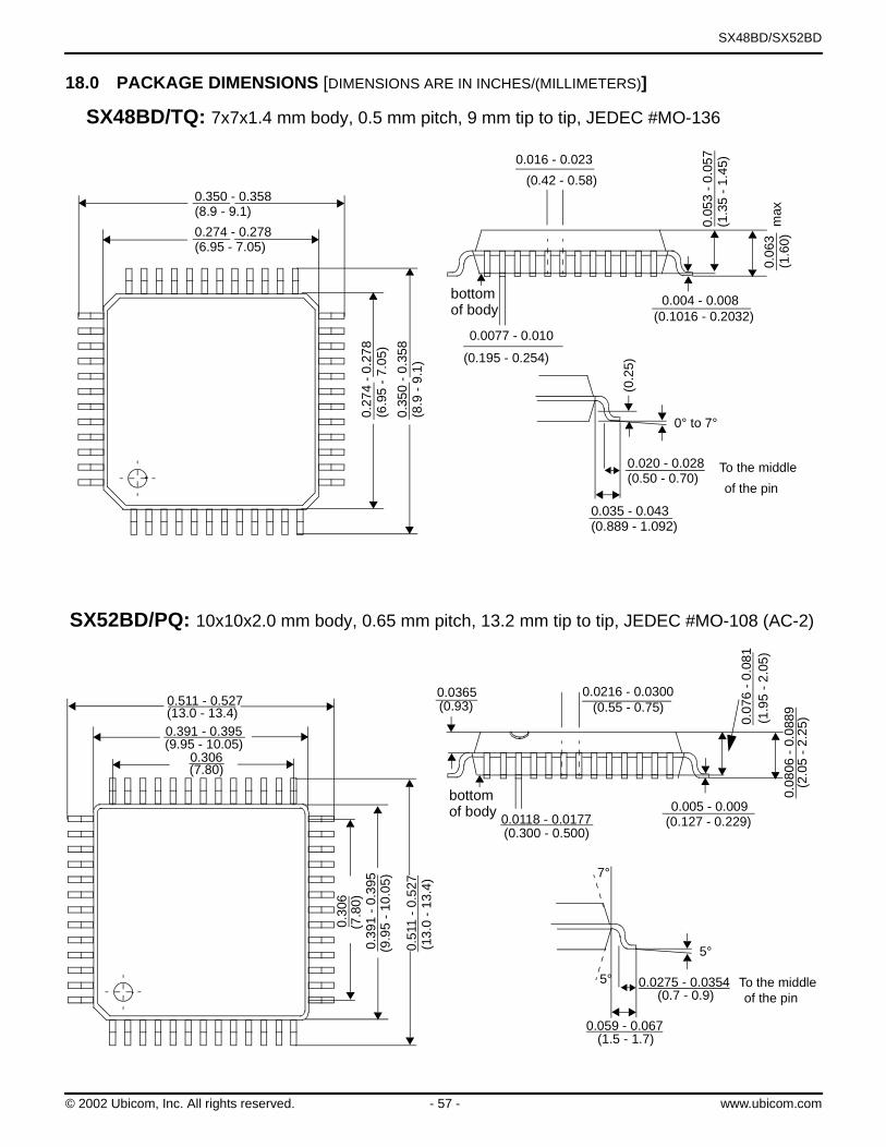
SX48BD/SX52BD
18.0 PACKAGE DIMENSIONS [DIMENSIONS ARE IN INCHES/(MILLIMETERS)]
SX48BD/TQ: 7x7x1.4 mm body, 0.5 mm pitch, 9 mm tip to tip, JEDEC #MO-136
0.350 - 0.358(8.9 - 9.1)
0.274 - 0.278(6.95 - 7.05)
0.35
0 -
0.35
8(8
.9 -
9.1
)
0.27
4 -
0.27
8(6
.95
- 7.
05)
0.035 - 0.043(0.889 - 1.092)
0.020 - 0.028(0.50 - 0.70)
(0.2
5)
0° to 7°
0.0077 - 0.010
0.06
3(1
.60)
0.05
3 -
0.05
7(1
.35
- 1.
45)
(0.1016 - 0.2032)
bottom of body
max
(0.195 - 0.254)
0.004 - 0.008
0.016 - 0.023
(0.42 - 0.58)
To the middle
of the pin
(1.5 - 1.7)
(0.7 - 0.9)
0.0118 - 0.0177(2
.05
- 2.
25)
(9.95 - 10.05)
(7.80)
(13.0 - 13.4)
(9.9
5 -
10.0
5)
(7.8
0)
(13.
0 -
13.4
) 7°
5°
(0.93)
5°
0.0365
0.08
06 -
0.0
889
(0.300 - 0.500)
0.51
1 -
0.52
7
0.39
1 -
0.39
5
0.30
6
0.511 - 0.527
0.391 - 0.395
0.306
0.0275 - 0.0354
0.059 - 0.067
bottom of body
0.0216 - 0.0300(0.55 - 0.75)
(0.127 - 0.229)0.005 - 0.009
0.07
6 -
0.08
1(1
.95
- 2.
05)
To the middleof the pin
SX52BD/PQ: 10x10x2.0 mm body, 0.65 mm pitch, 13.2 mm tip to tip, JEDEC #MO-108 (AC-2)
© 2002 Ubicom, Inc. All rights reserved. - 57 - www.ubicom.com
© 2002 Ubicom, Inc. All rights reserved. - 58 - www.ubicom.com
Sales and Tech Support Contact Information
For the latest contact and support information on SX devices, please visit the Ubicom website at www.ubicom.com.The site contains technical literature, local sales contacts, tech support and many other features.
635 Clyde Ave.Mountain View, CA 94043
Tel.: (650) 210-1500Fax: (650) 210-8715
E-Mail: [email protected] Site: www.ubicom.com
SX48BD/SX52BD
Lit #: SX-DDS-SX4852BD-13