Porting the Helix MP3 Decoder Onto Microchip's PIC32MX 32-bit ...

SWPM Power Inverter(using ATtiny25)
Hardware and Firmware Information
March 2019© Nikos Bovos

SPWM Power Inverter with ATtiny25© Nikos Bovos March 2019
Email: [email protected] / [email protected]
Disclaimer: This project is the author's work and provided with no guarantees of any form. Anyone who could use theinformation provided herein accepts the responsibility of his/her acts. Although hard work was made for the information tobe as accurate as possible, still there is no guarantee about any results or proper work of the unit when built differentfrom the author's design guidelines and/or notes. All information in this document are free for private/non-commercialuse. For commercial use, please contact the author. AVR is a trademark of Microchip Technology Inc. All other mentionedproducts/signs might be trademarks or registered trademarks of their respective holders and are referred where possible.For any further information, please contact the author.
1. Basic idea and requirementsThis is a project about a sinusoidal pulse width modulation (spwm) power inverter
“update”. The topology selected for this project is push-pull, by means that the output isequally driven by the power stages (a semi-period by each stage) - although spwminverters are usually based on full-bridge topology. The basic requirements:
a. Output RMS voltage 220 Volt AC (more on this later)
b. Frequency of the output signal 50Hz
c. Total RMS power by the inverter 300 Watt (more on this later)
d. Input Voltage 12V DC
e. Sine wave output waveform (more on this later)
Although 300 Watt RMS power selected for this project, the general terms andfunctions are the same for any power desired (more details will be presented during thisproject in order one will be able to construct the same project with more power).Thereason of 300 Watt is that I already have an 24 VDC / 230 VAC 750Watt RMS Powerinverter in my lab constructed a long time ago (in 2002) and I had build another inverter,the 48 VDC / 220 VAC 1500 Watt Sine Wave Inverter using Hexfet* transistors, presenteda long-long time ago (in 1997), as a project in graduating from Technological EducationalInstitute of Athens and get my diploma. Because that one constructed then and after awhile disassembled, this smaller inverter is the “reincarnation” of the older one, followingthe same principles that I used in that project (although with totally new approach). AlsoI've built a 12 VDC/230V AC 300Watt push-pull power inverter with modified square waveoutput (in 2003), which is the one that will be “updated” (although still working fine as it is).Whenever you see in the text “old brother” or “older inverter” or any similar, it is referred tothe 1997 sine wave one (whose the basic principles will follow). 230VAC or 220VAC wherereferenced are the same (I have a 2x9V/220V transformer, but now 230V AC became thestandard voltage in Greece, but loads can work with either of them).
The reason for presenting this one, is because it's smaller and easier to build.Previous inverters had at first uncontrolled output voltage, updated later (in 2012) forautomatic control by manually setting the desired output voltage. Why follow principles of1997 you may ask? That project was awesome for it's time, for me, gave me a grade ofperfect 10 and why not? Principles are still the same...I'm a principal guy!
Hexfet was a trademark of International Rectifier (1997), now acquired by Infineon Technologies
SPWM Push-Pull Power Inverter with ATtiny25 - Nikos Bovos - [email protected] March 2019 Page 1 of 19
2. Basic calculations and a little info
a. Maximum Power and currentThe inverter will be powered by 12 Volt direct current voltage provided from
batteries. Let's calculate the maximum currents (for DC and AC Side):
P = V*I and PMAX = 300 Watt , VDC = 12 Volt , so IDC = 300W/12V = 25 AOn the AC side we have P = 300Watt and V=230V, so IAC = 1,30 A
Given the above results, the fuses that we will use to protect each side, are:1) 25A - 30A Fuse (Fast) on the DC side2) 1,5A - 2 A Fuse (Fast) on the AC Side.
b. Operation and waveformThe operation of this inverter (and any other despite the topology) lies in the
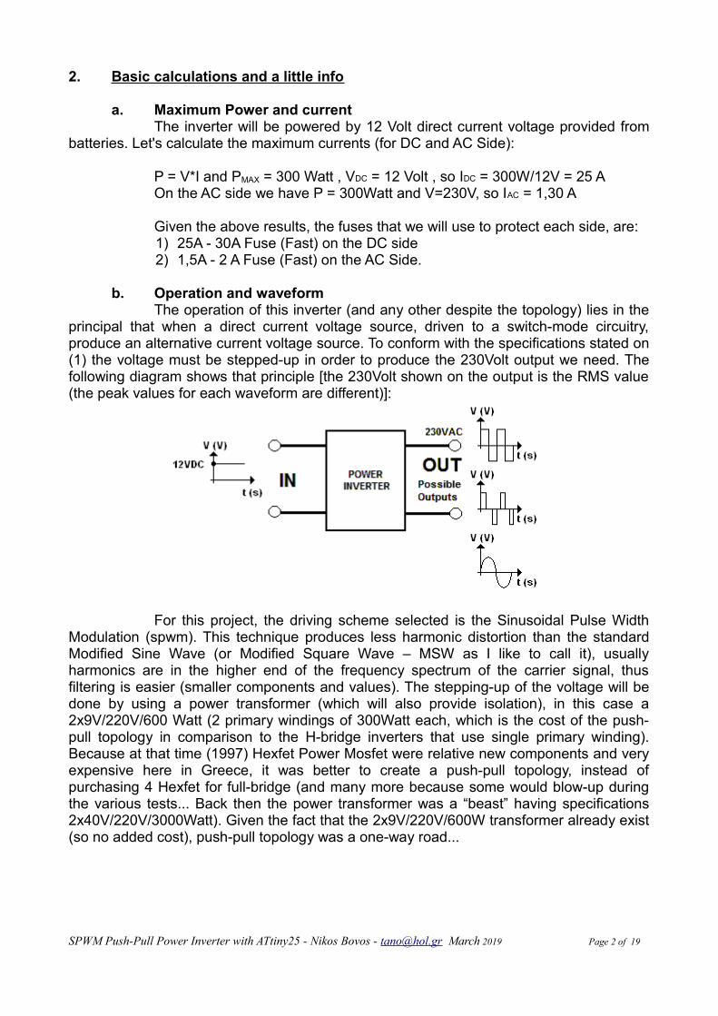
principal that when a direct current voltage source, driven to a switch-mode circuitry,produce an alternative current voltage source. To conform with the specifications stated on(1) the voltage must be stepped-up in order to produce the 230Volt output we need. Thefollowing diagram shows that principle [the 230Volt shown on the output is the RMS value(the peak values for each waveform are different)]:
For this project, the driving scheme selected is the Sinusoidal Pulse WidthModulation (spwm). This technique produces less harmonic distortion than the standardModified Sine Wave (or Modified Square Wave – MSW as I like to call it), usuallyharmonics are in the higher end of the frequency spectrum of the carrier signal, thusfiltering is easier (smaller components and values). The stepping-up of the voltage will bedone by using a power transformer (which will also provide isolation), in this case a2x9V/220V/600 Watt (2 primary windings of 300Watt each, which is the cost of the push-pull topology in comparison to the H-bridge inverters that use single primary winding).Because at that time (1997) Hexfet Power Mosfet were relative new components and veryexpensive here in Greece, it was better to create a push-pull topology, instead ofpurchasing 4 Hexfet for full-bridge (and many more because some would blow-up duringthe various tests... Back then the power transformer was a “beast” having specifications2x40V/220V/3000Watt). Given the fact that the 2x9V/220V/600W transformer already exist(so no added cost), push-pull topology was a one-way road...
SPWM Push-Pull Power Inverter with ATtiny25 - Nikos Bovos - [email protected] March 2019 Page 2 of 19

3. Circuits and components used
a) DC Input Voltage and power supplyThe battery (or batteries) that will be used in this project, must provide the
inverter with the necessary power. The type can be SLA, GEL or any other type. Voltage ofthese batteries can vary depending on their charged state. Under normal conditions, thevoltage in open circuit must be > 12.50 V (when fully charged with 2,275V/cell – at 13,65V)down to 11,80 Volt or less. When discharged, can reach 10,50V (ending discharging pointat 1,75V/cell for SLA type – or lower to 10,00Volts or less for other battery types). Theoperation is the same, the charging process is slightly different between for the differentbattery types (each manufacturer gives the details for their batteries).
Given the above situation, the power supply of the inverter can beconstructed using everyday components, found in anyone's self. A simple circuit diagramof the power supply of this inverter is presented below:
All schematics were made by using Bsch3V by H.Okada(Suigyodo) (c)1997-2014 , [email protected] for contacting the author.
The above circuit is straightforward, a typical 7805 circuit with furtherprotection. I used Texas Instruments LM7805 IC and it will be referred that way throughthis document, as well as any other IC used in this project. D1 is used to protect the circuitif polarity is reversed and diode D4 is used to protect the LM7805 if the output is shorted(providing a return path for reverse currents). The D3 diode is protecting the LM7805 thesame way for as the D4 and “takes” the reversed currents together with D2 to provide thereturn path to reverse currents. The two capacitors used, input 100nF to provide theLM7805 with filtered input and C2 for output (value 1uF to 10uF (or larger) to fit therequirements. In the final PCB the simple version used (with not all protection).
The “old brother” used a power supply circuit build around a SimpleSwitcher© LM2576HV step down switching regulator capable of providing 3A outputcurrent. This project does not have the same power requirements, so a simpler circuit isbuilt (you can use a variable regulator - LM317 or similar instead of LM7805). Also the oldone had 48V DC input voltage (and thus working with the HV version of LM2576), hereonly 12V DC will be the DC input voltage.
Simple Switcher was a trademark of National Semiconductor (1997) - now Texas Instruments after acquisition
SPWM Push-Pull Power Inverter with ATtiny25 - Nikos Bovos - [email protected] March 2019 Page 3 of 19

b) Sine and Triangle signals and production of spwm signal
In order to produce an spwm signal, a sinusoidal waveform and a trianglewaveform (of the same max and min amplitudes for best results) must be compared. Theproduct of this comparison, the spwm signal which will be used in driving the powerstages. For the sine and triangle reference waveforms, the older brother used two IntersilICL8038 analog function generator chips. This one will be build around a microcontroller,thus saving space, specifically a Microchip's AVR© 8bit RISC MCU (based on a modifiedHarvard architecture), that will be programmed to perform the necessary functions. Thesemicros can be programmed in Assembly, C, Pascal, Basic and others as well. Usually forsuch projects I prefer the Assembly language (although a little more messy and timeconsuming to do the programming)
In the older inverter, a nice trick was used... Instead of comparing a fullperiod of the reference sine-wave, only a semi-period was used and later “replicated” as itis symmetrical. To accomplish that, the sine waveform was rectified and thus producing thefollowing waveform (as shown a double-frequency waveform produced (100 Hz), but thiswas not a problem since the distribution circuits for the power stages used a 50 Hzreference signal, thus re-creating the correct sequence.
The new version will use an MCU... Of course the same principal can beapplied here also by means to produce the sine waveform (usually by using a lookuptable), pass it through a R-2R circuit, filter it out, produce the triangle waveform the sameway, produce the 100Hz and 50Hz square reference waveforms etc etc etc. To producethe sine-wave (at least to a good fidelity) a lookup table for at least 8 bits is needed andthe more the better. For the triangle also about the same stuff and not to mention that theautomatic voltage control will be implemented in the MCU as well, so probably these aretoo many jobs to do with this MCU (or at least too many jobs for me to do with this MCU).
So, in order to have the MCU do less jobs (and write less in the firmware) a“good trick” was used... The sine and triangle waveforms instead of the MCU, were bothproduced by a PC-Software of mine, the comparison made by the same software and theproduct of this comparison (the spwm signal) was produced also there... The times that thesquare waveform changes from 0V to 5V and from 5V to 0V were recorded on a table forfurther processing. The more high the triangle frequency, the more the comparisonsneeded and the lower the triangle frequency, fewer comparisons will be made. If insteadof triangle a high frequency sine waveform is used, yields to the same results (more orless – depending on the frequencies ratio).
AVR is a trademark of Microchip Technology Inc
SPWM Push-Pull Power Inverter with ATtiny25 - Nikos Bovos - [email protected] March 2019 Page 4 of 19

Some of the waveforms produced by the PC-software:
100Hz and 10kHz results
100Hz and 2kHz results
100Hz and 1kHz results
SPWM Push-Pull Power Inverter with ATtiny25 - Nikos Bovos - [email protected] March 2019 Page 5 of 19

The above figures show how the spwm signal is produced by comparing thereference and the high frequency sine waveform. The amplitude of the spwm signal is +5V(it is shown to have half the amplitude for cosmetic reasons - to be able to distinguish thechanges more easily). The old brother used two comparator circuits build around LM311voltage comparators, having the sine waveform in the non-inverting (+) input and thetriangle waveform in the inverting input (-).
With the above technique there is no need for negative power supply, whichwould be necessary if it was to compare a full-period (non-rectified) sine wave with thecorresponding triangle wave. Also the comparators circuits and power stages would needthis negative power supply to distinguish the signals, so space and complexity saved atthe same time.
Since microcontrollers have less processing power than computers, anothertrick was used... After finding the times of the comparisons, the table of values was furtherprocessed based on the clock frequency of the MCU calculating the ratio of the MCU clockversus comparison time. Since the output signal is in milliseconds (we want 50 Hz output)and the MCU clock usually is in nanoseconds (usually > 1MHz), the duration of transitionswas recorded. Further more another bunch of calculations made in accordance to Timerprescaler, in order to decide which Timer (and with what prescaler) is better to use andhow many interrupts would occur per period. The selected Timer will be configured forinterrupt on overflow. The table shown below is for 100Hz and 1kHz waveforms forMCUCLK = 2 MHz
Idx Time (s)spwm
(V)Duration
(μs)MCUClock
MCUClocks
Tmr8(250 kHz)
Tmr64(31.25 kHz)
Tmr256(7.812 kHz)
Tmr1024 (1.953kHz)
1 910 μs 5 V 910 μs 500 ns 1820 228 28 7 2
2 1113 μs 0 V 203 μs 500 ns 406 51 6 2 0
3 1820 μs 5 V 707 μs 500 ns 1414 177 22 6 1
4 2222 μs 0 V 402 μs 500 ns 804 101 13 3 1
5 2727 μs 5 V 505 μs 500 ns 1010 126 16 4 1
6 3335 μs 0 V 608 μs 500 ns 1216 152 19 5 1
7 3637 μs 5 V 302 μs 500 ns 604 75 9 2 1
8 4445 μs 0 V 808 μs 500 ns 1616 202 25 6 2
9 4547 μs 5 V 102 μs 500 ns 204 25 3 1 0
10 5455 μs 0 V 908 μs 500 ns 1816 227 28 7 2
11 5558 μs 5 V 103 μs 500 ns 206 26 3 1 0
12 6365 μs 0 V 807 μs 500 ns 1614 202 25 6 2
13 6668 μs 5 V 303 μs 500 ns 606 76 9 2 1
14 7275 μs 0 V 607 μs 500 ns 1214 152 19 5 1
15 7780 μs 5 V 505 μs 500 ns 1010 126 16 4 1
16 8183 μs 0 V 403 μs 500 ns 806 101 13 3 1
17 8890 μs 5 V 707 μs 500 ns 1414 177 22 6 1
18 9092 μs 0 V 202 μs 500 ns 404 51 6 2 0
19 10000 μs 0 V 908 μs 500 ns 1816 227 28 7 2
Table 1 – Calculations for 1 kHz spwm signal for fMCU = 2 MHz
SPWM Push-Pull Power Inverter with ATtiny25 - Nikos Bovos - [email protected] March 2019 Page 6 of 19

The last entry is to complete one semi-period (output is still 0V during thistime, so no transition is made). All values were rounded to the nearest integer (% of erroris negligible). “Typical” prescaler values used, although some Timers on AVRs have also16, 32 and other prescaler settings, but since many values can do the job, no need toover-calculate ! All other tables for the frequencies used are calculated in the same way. Itis easily seen that prescalers 256 and 1024 can't be used for the selected MCU clockfrequency, since there are too few ticks per interrupt, so one of the others will be used.
The final decision was made to use the prescaler value = 8 (for 250 kHztimer frequency) for the 1 kHz spwm signal. Timer0 will be used and configured togenerate an overflow interrupt for the spwm signal generation and Timer1 will beconfigured to generate an overflow interrupt for each semi-period (every 10ms). Timer1will be configured for prescaler = 256 (thus 7812.5 Hz frequency). To generate anoverflow interrupt need 78 ''ticks'' (because 78 * (1/7812.5) = 9.984ms). The period TTMR1 =2 x 9.984ms = 19.968ms or FTMR1 = 50,08 Hz which is what we want to produce (with %error approximately 0,16% which is practically nothing...) and so the start-up value ofTimer1 will be 255 - 78 = 177 (or $B1 in hexadecimal).
After prescaler selection, a new table was constructed in order to find thestart-up values of Timer0. Because Table1 display 'clock ticks' needed by Timer0 to reachthe desired time, there is no need to have the mcu do the calculation, we will calculate theactual values needed to load Timer0 to perform the counting. The values to load Timer0are calculated as 255 – value as with Timer1 (both are 8-bit counters)
Idx From (s) To (s)Duration
(μs)Output (V) MCU Clocks
Timer0Ticks
(CLK / 8)
Timer0StartupValue
1 0 μs 910 μs 910 μs 0 V 1820 228 27
2 910 μs 1113 μs 203 μs 5 V 406 51 204
3 1113 μs 1820 μs 707 μs 0 V 1414 177 78
4 1820 μs 2222 μs 402 μs 5 V 804 101 154
5 2222 μs 2727 μs 505 μs 0 V 1010 126 129
6 2727 μs 3335 μs 608 μs 5 V 1216 152 103
7 3335 μs 3637 μs 302 μs 0 V 604 75 180
8 3637 μs 4445 μs 808 μs 5 V 1616 202 53
9 4445 μs 4547 μs 102 μs 0 V 204 25 230
10 4547 μs 5455 μs 908 μs 5 V 1816 227 28
11 5455 μs 5558 μs 103 μs 0 V 206 26 229
12 5558 μs 6365 μs 807 μs 5 V 1614 202 53
13 6365 μs 6668 μs 303 μs 0 V 606 76 179
14 6668 μs 7275 μs 607 μs 5 V 1214 152 103
15 7275 μs 7780 μs 505 μs 0 V 1010 126 129
16 7780 μs 8183 μs 403 μs 5 V 806 101 154
17 8183 μs 8890 μs 707 μs 0 V 1414 177 78
18 8890 μs 9092 μs 202 μs 5 V 404 51 204
19 9092 μs 10000 μs 908 μs 0 V 1816 227 28
Table 2 – Calculations for start-up values of Timer0 for 1kHz spwm
SPWM Push-Pull Power Inverter with ATtiny25 - Nikos Bovos - [email protected] March 2019 Page 7 of 19

ATtiny25 is equipped with 128 bytes of internal non-volatile eeprom and 128bytes of internal volatile static ram. It has also 2 kbytes of non volatile program flashmemory, so the necessary time-values will be stored in one of these memory spaces. Itcan be configured for internal clock or external clock, external crystal or resonator. Theclock that will be used is external crystal at 2.000 MHz because I have many availablefrom past projects (any other crystal can be used as long as the calculations will be donefor that clock frequency), along with two 22pF ceramic capacitors. The internal fuses of theMCU were programmed as: CKSEL [3:0] = 1010 for external crystal or ceramic resonator(0.9 MHz to 3.0MHz) and the Clock Divide by 8 fuse (CKDIV8) was disabled (un-programmed to 1). Please note! In AVR microcontrollers fuses '0' means programmedwhilst '1' means un-programmed.
ATtiny25 has six programmable I/O lines on PORTB (PB0 to PB5), wherePB5 will be used as RESET and the rest for the various functions. The port-map of themicrocontroller used in this project is presented below:
Port pin Function / Description Direction
PB0 SPWM Signal for channel #1 OUT
PB1 SPWM Signal for channel #2 OUT
PB2 ADC1 input for automatic voltage regulation IN
PB3 XTAL1 for 2 MHz crystal IN
PB4 XTAL2 for 2 MHz crystal IN
PB5 Used as RESET (user configuration doesn't mind) IN
In the next chapter the automatic voltage regulation will be analyzed, alongwith some more information about the microcontroller.
A must-say note! Although no code accompany this document, theguidelines and information provided here are more than enough for anyone with ''typicalknowledge'' to build this project and adjust it for his/her own needs. Because I spent toomuch of my – not so free - time to construct, write, build, test, update etc I'm awfullyirritated when I'm asked to provide the full listing for ''copy & paste” from others. I'm sorryto say that, but buying 2 boards, connect them with 2 cables and writing two lines of codeto your computer does not help you in any way to learn how and more important why itworks (even if that LCD screen is displaying 'Hello world !')...It's better to try and fail andthen to repeat until you get it and learn a lot in the process, than to get the “working code”from others without even scratching your brain on how to do it.
SPWM Push-Pull Power Inverter with ATtiny25 - Nikos Bovos - [email protected] March 2019 Page 8 of 19

c) Automatic output voltage regulation (AVR)
This project will have the ability to stabilize the output RMS voltage to the'desired' value (here 220V AC). The existing MSW inverters I've built, do the same,according to the selection of the user (by using a potentiometer in the front panel), so theycan theoretically produce output values from 0V to 300V (although 99% of the timesthey've been used for 220V AC output RMS voltage whenever a utility black-out occur).This is accomplished by varying the duty cycle of the MSW signal (modified square wave –suitable for 90% of the devices at home - or modified sine wave as the advertisements liketo refer to it). In this project regulation will be done automatically (no user intervention).
Unfortunately, it is “forbidden“ to touch the duty cycle of the signal - as it isnot a MSW signal, so there are really only two available options. The first is to modify thepeak voltage of each pulse (by using multiple windings in output transformer or variableDC input) and the second is to modify the frequency of the pulses of the spwm signal(which is what we are going to do, since the existing transformer will be used).
Before entering to this, a little more information about how the automaticvoltage regulation will be done... In the output of the inverter, a simple circuit built toreference the output voltage, as shown in the following schematic:
Not much to over-analyze for the above circuit... Output is stepped-down by aPCB-transformer to ''MCU-acceptable'' levels. Then rectified, filtered and then it is dividedby the voltage divider that consisted by resistors R1 and R2 and then driven to the ADCinput of the MCU (to PB2 input as shown on the port-map before). The Zener diode isthere to protect the input pin of the MCU if the input voltage exceed 5,1 Volt (which isnearly impossible for the current setup). The above circuit was adjusted to provide to theMCU pin VPB2 = 3,003 V, when the output voltage is 220V AC. The capacitor's value (68μF- 100μF) selected is one that is not too big to loose small changes of output voltage, nortoo small to have rippling (and give wrong results - the A/D of MCU has a very goodresolution). A good test is to measure with oscilloscope/voltemter the rippling to find thegolden rule . A table of values could be constructed with the levels of the output rmsvoltage versus the corresponding A/D values, but it's easy to calculate for yourself.
In order to automatically regulate the output voltage, it's unrealistic to stick to220V RMS voltage (although not impossible since A/D has good resolution). A realisticapproach is to define a ''safe window'' of acceptable voltage (and regulate when voltage isoutside this window). The margin chosen is 4 Volt (nearly nothing), so we will acceptoutput voltages for RMS values between 218-222 Volt (or 228-232V for 230V output). Weare not trying to create a ''stabilizer'' here, but to have a voltage source that can be usedwith the loads we have at home (although still not impossible for smaller ''window'').
SPWM Push-Pull Power Inverter with ATtiny25 - Nikos Bovos - [email protected] March 2019 Page 9 of 19

ATtiny25 features a 10-bit successive approximation Analog to DigitalConverter with 4 single ended channels (or 2 differential channels) and temperaturemeasurement capability. ADC1 input (PB2) will be used to measure the input signal fromthe feedback circuit. For single-ended channel 10-bit resolution the result is given by:
(datasheet states 1024, but result is 1023 (1024 are the A/D 'steps'
from 0 to 1023). Highest ADC result is $3FF = 1023 (1024 minus one LSB) and lowestresult is $00 (as with all 10bit A/D converters). The reference of the ADC was selected tobe VREF =VCC = 5V and so for 10-bit resolution each ADC measurement 'step' will be 5V /1024 = 4,88mV (for 5.00V power supply). For the selected voltage window, we calculateminimum and maximum acceptable values as ADCMIN = 2,974V (this is translated by A/Das $261) and ADCMAX = 3,027V ($26C). So we will have a safe window of $26C - $261 =$0B or 11 A/D 'steps'. The previous values were setup to microcontroller to be comparedwith the result of the A/D conversion. If more or less safe window needed, the abovevalues can be changed accordingly.
The A/D converter was setup for prescaler = 32 (by setting ADPS2=1,ADPS1=0, ADPS0=1 in ADCSRA register) thus having clock with f=62,5 kHz. Eachconversion according to the datasheet takes about 13 ADC clock cycles (after the firstconversion), or about 200 μs. The A/D converter configured for free-running mode (bitsADTS2=0, ADTS1=0, ATDS0=0 in ADCSRB register). The first A/D conversion howevermust be started by the user by setting ADSC bit in ADCSRA (using sbi ADCSRA, ADSC)
To be able to regulate the output voltage, in each period of the output signalthe A/D is comparing the ADC result to the maximum and minimum values setup on themcu (this is done about every 100 A/D conversions or 20ms). As stated before, we can'ttouch the duty cycle of the spwm signal and must stay in that form in order to reproduce asine wave in the output, so the realistic approach is to change the driving scheme withhigher frequency when we want lower output voltage, or lower frequency when we wanthigher output voltage (and always keep the spwm form of driving). The value from ADCused, is the full 10-bit (could also use 8-bits, by setting ADLAR=1 in ADMUX I/O registerand read ADCH register value only, but didn't need that, so the full 10-bit result isprocessed).
On previous page, the table of the values for one driving scheme (spwm for1kHz) is shown. For the current setup (battery, transformer, Hexfet etc) six of thesetables defined, from 400Hz to 2000Hz to fit various loads and saved in flash memory ofthe MCU. For your setup maybe a different frequency scheme might be needed... To dothe automatic output voltage regulation, the mcu start from the highest frequency (whichgives the lowest RMS output voltage) and then switch tables according to the result of theA/D comparison (or stays on the same table if the output voltage is within the acceptedlimits). One final note, is that the prescaler of Timer0 is changed according to the drivingscheme needed (because for every table a different Timer0 prescaler value is needed, forinstance 1 kHz spwm driving need prescaler = 8, while 600 Hz need prescaler = 64). Onelast note, if the lowest frequency (400Hz) fail to have the output voltage within the limits,then the mcu automatically switch to 50% and 60% Modified Square Wave (MSW) drivingas on the existing PCB and fall back to SPWM driving when “allowed”. Why higher spwmfrequency produces lower voltage? Because on-times of pulses are smaller than in MSWand so the total Root Mean Square (RMS) value is lower.
SPWM Push-Pull Power Inverter with ATtiny25 - Nikos Bovos - [email protected] March 2019 Page 10 of 19

d) Drivers and output power stages
Another critical note! The ''comfort zone'' of 5V low current mcuenvironment is long gone here If you plan on building this project. Extra care must betaken, high currents are produced in this part of the project, capable of doing damage !Use adequate cables and connectors and take all safety measures (even wear protectiveglasses when lean above to work on these PCBs. Any mistake or short-circuit will ''kill''components instantly spreading their pieces around. Double-check everything beforepower up! Please don't mess with this, if you are not 100% sure of what you are doing !
The spwm signal produced by the MCU is at a voltage level capable ofdriving logic-level Mosfet transistors, but not at necessary power for fast switch-on.Because the existing boards of the MSW inverter will be used, the following is the existingcircuit from 2003 (which have standard level Hexfet Power Mosfet Transistors).
A few words about the above circuit...U1 is a LM311 voltage comparator thatproduces +12V from +5V input pulses. R3 variable resistor set a low voltage (~ 300mV) onthe non-inverting input to avoid the possibility of oscillation when both pins are 0 volt - dueto the high open gain of the comparator. Transistors Q1 and Q2 form a 'totem pole' with lowimpedance output path. These are switching transistors (BD239 and BD240 but any pair ofNPN/PNP switching transistors can be used capable to charge Mosfet's C ISS). TransistorQ1 drives the Hexfet Power Mosfet Transistors, whereas Q2 provide a return path forreverse currents (can be omitted if you trust the two diodes speed) when Q3 is switching-off and driving signal is 0 volt. R1 is typical < 10Ω providing a low impedance path toMosfet's Gate. D1 is a 12V Zener diode to protect Mosfet's Gate from over-voltage (by notallowing voltage to exceed maximum VGS). D2 is a fast recovery small signal diode(1N4148 or similar) and provide a return path of induced currents by the Source. Q3 isconsisted of two IRFP250 Hexfet Power Mosfet transistors connected in parallel (each oneis 30A/200V), whereas D3 is an 60EPU02 Ultrafast Soft Recovery Diode (60A/200V). R2 isa varistor (V130K14) protecting the D-S junction of the Mosfets (clamping excessiveinduced voltages to about 170V DC) and finally transformer T1 is the existing center-tapped 2x9V/220V/600Watt. Bypass capacitors are 0,1μF/16V tantalum or similar for allICs used. The other leg not shown is exactly the same, only the input to comparator isfrom PB1 pin of the microcontroller.
SPWM Push-Pull Power Inverter with ATtiny25 - Nikos Bovos - [email protected] March 2019 Page 11 of 19

Since we are using a push-pull topology, all references are to the commonground (the battery '-') so there are no floating parts - as with full bridge circuits where theupper leg components are at the output voltage level and thus need a bootstrap / drivingcircuit. Here a simpler driving scheme is used. The above circuit has proven to be veryrobust all these years, whenever it had (and has) to operate. The big brother 24V/750Wattalso uses the same circuit for each leg but with different components. An optional R-C orR-C-D snubber circuit can be used (aiding the Mosfet Transistors at switch-off with typicalvalues 33-47 Ω and capacitor of 10nF) placed in parallel to the D-S junction. ''Usually'' forall other Mosfet circuits are omitted except for chopper applications. For the existingboards, no snubber circuits exist, without any problems with various types of loads (atleast so far...).
If higher output power is desired, output power transformer and Mosfettransistors need to be changed accordingly and the protective diodes if existing ones arenot sufficient. Cables and connectors also to handle the necessary current (usually I uselarger diameter cables and connectors, to avoid any voltage drop and heat on the cablesand to be sure that they can withstand more than the current needed by the application, somost of the times when upgrading a circuit it's not necessary to change the cabling).
A quick note about the external anti-parallel ultrafast recovery diode... PowerMosfet Transistors have an anti-parallel diode build-in in it's body. Usually (and thisdepends on the application) it's a good practice to have an external diode to increase theprotection level. For instance, the internal diode of IRFP250 has reverse recovery time ofmax. 280ns (IRF datasheet). If this is not enough (high dv/dt exist, an ultrafast (35ns)external diode is used. Newer Mosfet have faster and more robust characteristics for theirinternal diode and capabilities - check with datasheet – here the old 2003 circuit is used sothese information apply and the external diodes were mandatory.
A quick note about filtering... spwm is multi-pulsed-signal so you need to filterthe voltage waveform. Usually an L-C filter designed for 1/10 the carrier frequency ofspwm signal will give enough attenuation to the higher order harmonics. More later...
A quick note about Mosfet voltage selection. Even though we have ''only''12V input DC voltage, on inductive loads (and the power transformer is an inductive loadfor the Mosfet transistors) induced voltages occur at switching times (at turn-off). Thesecan be as large as 10 times or more the switching voltage, thus the Mosfet transistorsselected have VDSS = 200V. If any 40V or 50V Mosfet were used, probably they would bedestroyed relatively quick after power-up. In general, for switching applications is a goodpractice to select components with capability to withstand 10 times the switching voltage –although we use a varistor for protection, sometimes they are not ''quick enough'' for thedv/dt of the induced voltage. Again, newer components have better characteristics andprotections, see their datasheet, but in general it's a good practice to select componentswith maximum ratings higher than the ratings of the application (a little more costly butsurely worth it to save the most expensive components).
A quick note about transformer selection. This is a small headache, becausethe “correct” transformer depends on the spwm carrier frequency. Unfortunately for mysetup I had available the 2x9V/220V for the MSW so I stick to that. A greater ratio i.e2x6V/220V would allow higher driving frequencies and thus smaller filters, but this wasavailable to work with so a few compromises made...
SPWM Push-Pull Power Inverter with ATtiny25 - Nikos Bovos - [email protected] March 2019 Page 12 of 19
4. Construction and testing
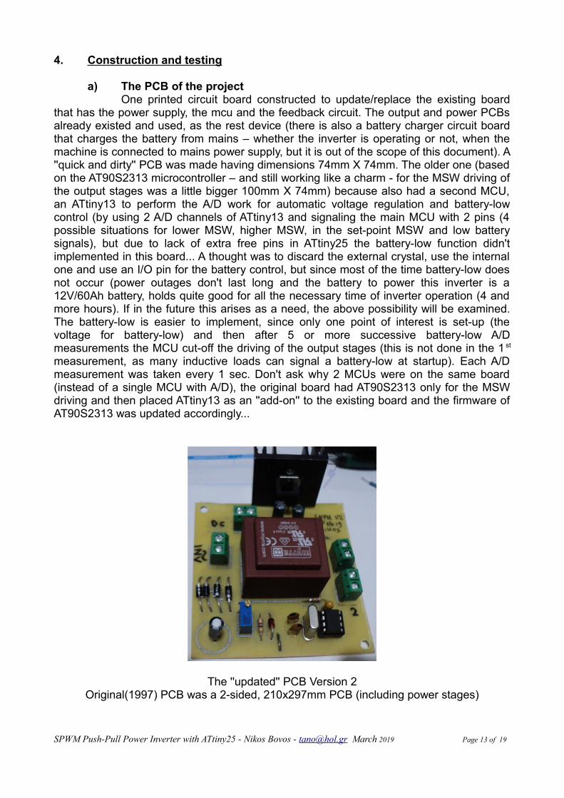
a) The PCB of the projectOne printed circuit board constructed to update/replace the existing board
that has the power supply, the mcu and the feedback circuit. The output and power PCBsalready existed and used, as the rest device (there is also a battery charger circuit boardthat charges the battery from mains – whether the inverter is operating or not, when themachine is connected to mains power supply, but it is out of the scope of this document). A''quick and dirty'' PCB was made having dimensions 74mm X 74mm. The older one (basedon the AT90S2313 microcontroller – and still working like a charm - for the MSW driving ofthe output stages was a little bigger 100mm X 74mm) because also had a second MCU,an ATtiny13 to perform the A/D work for automatic voltage regulation and battery-lowcontrol (by using 2 A/D channels of ATtiny13 and signaling the main MCU with 2 pins (4possible situations for lower MSW, higher MSW, in the set-point MSW and low batterysignals), but due to lack of extra free pins in ATtiny25 the battery-low function didn'timplemented in this board... A thought was to discard the external crystal, use the internalone and use an I/O pin for the battery control, but since most of the time battery-low doesnot occur (power outages don't last long and the battery to power this inverter is a12V/60Ah battery, holds quite good for all the necessary time of inverter operation (4 andmore hours). If in the future this arises as a need, the above possibility will be examined.The battery-low is easier to implement, since only one point of interest is set-up (thevoltage for battery-low) and then after 5 or more successive battery-low A/Dmeasurements the MCU cut-off the driving of the output stages (this is not done in the 1 st
measurement, as many inductive loads can signal a battery-low at startup). Each A/Dmeasurement was taken every 1 sec. Don't ask why 2 MCUs were on the same board(instead of a single MCU with A/D), the original board had AT90S2313 only for the MSWdriving and then placed ATtiny13 as an ''add-on'' to the existing board and the firmware ofAT90S2313 was updated accordingly...
The ''updated'' PCB Version 2Original(1997) PCB was a 2-sided, 210x297mm PCB (including power stages)
SPWM Push-Pull Power Inverter with ATtiny25 - Nikos Bovos - [email protected] March 2019 Page 13 of 19

b) Waveform filtering
As stated, SPWM signal is a multi-pulsed signal so it must be filtered out inorder to be accepted by the loads. The ''old brother'' used 30 kHz carrier for the spwmsignal and the filtering was done in the input (primary of the transformer), by constructingtwo “big” air inductors of 330μH each, with wire capable of delivering 35A and it was a realchallenge to make them (the transformer primary usually has low inductance valuecompared to the much higher inductance of the secondary)... The capacitors used were33μF non-polarized, thus giving two low-pass filters (one for each leg) with cutofffrequency (-3db) approximately f=1,5 kHz. The output waveform was a good sine-wavewith low THD (the attenuation on the 30kHz carrier was more than 100db) and transformernoise was eliminated.
In this setup, unfortunately the carrier frequency is much smaller (MSW 50%,MSW 60% and SPWM 400Hz up to 2kHz) and I didn't want to challenge myself again witheven bigger inductors in the primary this time, so the filtering was made in the secondaryof the transformer, sacrificing the ''transformer noise'' and sacrificing a little of the efficiencyalso. Because of the secondary big inductance (> 10H) only a capacitor filter placed inparallel to the secondary winding. After a few tests, the finalized value is 10μF (composedby 10 capacitors of 1μF/630V polyester non polarized, connected in parallel). For thisperiod and the available time that I don't have, it's more than fine... Either way, I wanted toexperiment more on the waveform and the automatic regulation, than to have the cleanestsine wave in the output (not impossible though if you can wind the needed primary air-coreinductors).
SPWM Push-Pull Power Inverter with ATtiny25 - Nikos Bovos - [email protected] March 2019 Page 14 of 19

c) Installation and tests
The board installed and inverter powered-up for load = 100 Watt (30%).
The board is sitting on top of the existing one. Apart from the new board, thetwo output & power stages are shown. Behind the two heat sinks there is a 12V DC fan,the battery is shown under the boards on the right is a car battery 12V/60Ah). The outputtransformer is in the left-back side and not shown. In the bottom is just visible the batterycharger circuit. The ''big cables'' connect the Drain of the parallel Mosfets to Transformerprimary winding and the Source to battery negative (ground). The high current connectionsas seen is made with nuts and bolts... Overall it's a heavy metal construction (exceeding20 kg, since the car battery itself is > 10 kg) and it is placed on four wheels for easytransportation whenever is needed to operate.
SPWM Push-Pull Power Inverter with ATtiny25 - Nikos Bovos - [email protected] March 2019 Page 15 of 19

For 100 Watt load, the waveforms of the old PCB and the new PCB were''taken'' (photographed), with and without output filtering. The tests that conducted were forfiltering by the (total) capacitor of 10μF.
For the MSW inverter this filter smooths too much the waveform, whilstwithout filter is the classic MSW waveform (the MSW driving is done a 50 Hz only and youcan't hear the transformer). In the spwm driving PCB filtering is mandatory becauseotherwise the waveform can't be used with normal loads (a photo was taken also). Allphotos were taken for 220 – 230VAC. The ''noise'' of driving is audible.
The oscilloscope (a Hameg 303-4) was setup for 5ms/div on X-axis and 100V/div onY-axis (10V x10 on probe). The output frequency of the signal was measured at 50 Hz by amultimeter and on the screen of the oscilloscope. Load on all photos is 100W (30%).
The old ''standard'' 50Hz MSW (no filter) of the old PCB (the above is for Duty Cycle approximately 70%)
SPWM Push-Pull Power Inverter with ATtiny25 - Nikos Bovos - [email protected] March 2019 Page 16 of 19

The ''updated'' SPWM waveform without filters (600 Hz driving)
The SPWM waveform with 10μF output filter (600Hz driving)
SPWM Push-Pull Power Inverter with ATtiny25 - Nikos Bovos - [email protected] March 2019 Page 17 of 19

The SPWM waveform with 10μF output filter (1 kHz driving)
“Heavy filtered” and attenuated (with L=4mH, C=10μF) for 600Hz driving(RMS value of the above is 195V AC)
SPWM Push-Pull Power Inverter with ATtiny25 - Nikos Bovos - [email protected] March 2019 Page 18 of 19

The Modified Square Wave mode (MSW) when “heavy loaded” (70% Load)The above refers to D=60% with the 10μF output filter
Overall the project can be characterized as success (at least for me so far)...The output is holding to the predefined values and the switching of tables when changingloads or if voltage drops/rises outside the defined window was perfect. One point thatcould be better was, if the transformer ratio was not that small and had a higher ratiotransformer (2x6V/220V instead of 2x9V/220V). That would have better results and allowhigher frequency driving - but it was not available, so I had to work with the current setup...
The firmware of the MCU was programmed in Assembly. The final assembledfile is 616 words (occupying only 30% of the mcu flash memory – which has 2048 bytes),so there is plenty of room for any future expansion or update...
One may ask...Why ATtiny25 ? Well if you want to go to the corner of yourstreet, then you don't go with your car, but you go on foot instead ! Since ATtiny25 can dothe job just fine, there is no really need to use an ATMega with 100 pins, to use just 3 !Maybe if you program in C or Basic etc the alternatives could be ATtiny45 or ATtiny85(same mcu with larger memories), but really there is no need to select a so much biggermicrocontroller than the one that can do the job fine. That's why they have so manymodels, to choose the one for the job...
Overall it worked as expected and I'm more than pleased with the results...More to come if the free time is found somewhere... Up to this point, thanks for baring withme and reading so far... Any comments or suggestions would be very much appreciated...Any donations via paypal to [email protected] would be very much appreciated also...Comments or questions I would gladly answer if the answer is not already in this document(otherwise I will use the well-known RTFM !!!)
Until the next time be well... See ya !
SPWM Push-Pull Power Inverter with ATtiny25 - Nikos Bovos - [email protected] March 2019 Page 19 of 19