SWITCHING VOLTAGE REGULATOR AND VARIABLE … · OPERATIONAL AMPLIFIER LM741 ... of the filter with...
30
1 SWITCHING VOLTAGE REGULATOR AND VARIABLE CURRENT LIMITER ARENDEL RICHARDS YUN TANG PETER TU JEFFREY WHITE ADVISOR: DR. MICHAEL CAGGIANO DEPARTMENT OF ELECTRICAL AND COMPUTER ENGINEERING 14:332:468 CAPSTONE DESIGN – ELECTRONICS SPRING 2013
Transcript of SWITCHING VOLTAGE REGULATOR AND VARIABLE … · OPERATIONAL AMPLIFIER LM741 ... of the filter with...

1
SWITCHING VOLTAGE REGULATOR AND VARIABLE CURRENT LIMITER
ARENDEL RICHARDS
YUN TANG
PETER TU
JEFFREY WHITE
ADVISOR: DR. MICHAEL CAGGIANO
DEPARTMENT OF ELECTRICAL AND COMPUTER ENGINEERING
14:332:468 CAPSTONE DESIGN – ELECTRONICS
SPRING 2013

2
TABLE OF CONTENTS
COVER PAGE ................................................................................................................................................. 1
TABLE OF CONTENTS .................................................................................................................................... 2
ABSTRACT ..................................................................................................................................................... 3
TRANSFORMER-RECTIFIER-FILTER ............................................................................................................... 4
9-0-9 TRANSFORMER ....................................................................................................................... 4
RECTIFIER ......................................................................................................................................... 4
FILTER ............................................................................................................................................... 6
VOLTAGE INVERTER ...................................................................................................................................... 7
BACKGROUND .................................................................................................................................. 7
PROJECT SPECIFICATIONS ................................................................................................................ 8
555 TIMER ..................................................................................................................................................... 9
BACKGROUND .................................................................................................................................. 9
PINOUT ........................................................................................................................................... 10
INTERNAL CIRCUITRY IN RELATION TO PINOUT ............................................................................ 11
DIFFERENT CONFIGURATIONS ....................................................................................................... 12
CONCLUSION .................................................................................................................................. 15
SWITCHING REGULATOR ............................................................................................................................ 16
LINEAR vs. SWITCHING................................................................................................................... 16
SWITCHING OPERATION ................................................................................................................ 17
BUCK CONVERTER CONFIGURATION ............................................................................................. 19
MOSFETs & BJTs ............................................................................................................................. 21
CURRENT LIMITER ...................................................................................................................................... 22
LINEAR REGULATORS ..................................................................................................................... 22
SELECTION OF REGULATOR............................................................................................................ 23
CONSTANT vs. FOLDBACK .............................................................................................................. 24
OPERATIONAL AMPLIFIER LM741 .................................................................................................. 25
LM741 PINOUT ............................................................................................................................... 26
VARIABLE CURRENT LIMITING CIRCUIT ......................................................................................... 27
TESTING .......................................................................................................................................... 28
DIVISION OF LABOR .................................................................................................................................... 29
REFERENCES ................................................................................................................................................ 30

3
ABSTRACT:
One of the main hazards in electrical or electronic circuits is over-current, or an excessive amount of
current being delivered to the load due to a short circuit.
Circuits can be protected from over-current by simple means such as using a fuse. As the current exceeds
the fuse’s limits, it blows and therefore disconnects the load from the source, preventing further current
from damaging the load. This is common method for protecting house-hold mains. A similar device is the
circuit breaker. While fuses are simple and secure, the drawback is that once they are blown, they need
to be replaced or reset.
A much more efficient method is implementing an active current limiting circuit. Because a fuse is a
passive element, it alone may not be able to protect internal devices from over-current, as it is generally
too slow in operation and the time it takes for it to blow may be enough to destroy the devices. An active
current limiting circuit sets a maximum load current by using sensing resistors along with transistors that
act as on and off switches.
Our project explores how current can be limited independent of the input voltage by passing signals
through various circuits including a transformer, rectifier, filter, and regulator.

4
TRF – 9-0-9 TRANSFORMER:
The power supply used in this project comes from a wall socket. These wall sockets provide a 120V, 60-
cycle AC power. The difference between AC (alternating current) and DC (direct current) is that while DC
power sources, such as batteries, fuel cells, and solar cells, has current flowing in the same direction
between two terminals, the direction of the current in AC sources reverses, or alternates, at 60 times
per second.
The big advantage of using an AC source is that it is easy to change the voltage of the power, using a
device called a transformer.
This integrated circuit starts off with a step down transformer 9-0-9. It is a symmetrically balanced
transformer relative to the output on the secondary side. In this case there is a 120V AC coming from
the wall into the primary. This 120V is stepped down to 18V AC on the secondary. However, this 18V AC
output can be tapped in the center with a ground of 0V AC and therefore splitting it into perfect halves
where the result is now two 9V AC terminals that are of opposite polarity. Hence the name 9-0-9,
meaning 9V AC on the output line terminal, 0V AC because of the center tapped to ground, and 9V AC
on the neutral terminal as shown in the diagram below.
RECTIFIER:
The significance of this configuration is that the two 9V AC terminals are now in opposite polarity. So,
like opposing magnets, the fields cancel. This provides symmetrically balanced power which contributes
to noise reduction because it cancels common mode noise, making the signal more efficient and linear
across a huge bandwidth. This also allows the effective use two diodes in creating a full wave rectifier as
opposed to the typical full bridge, 4 diode configurations. With this balanced output and two diodes, a
full wave rectifier is created that allows the conversion of incoming AC power to DC.

5
The signal leaving the transformer and prior to going through the diodes is sinusoidal as shown below.
The signal leaving the rectifier is no longer a sinusoid, but a pulsed, or rippled, DC signal. This is shown
below.

6
TRF – FILTER:
A capacitor is used in parallel between the rectified signal and the load. This will smooth out the ripple
and produce a fairly smooth horizontal signal which is the desired response for a DC signal.
When this filter is used, the RC charge time of the filter capacitor must be short and the RC discharge
time must be long enough to eliminate ripple action. In other words, the capacitor must charge up fast,
preferably with no discharge at all. Better filtering also results when the input frequency is high, thus
leading to the choice of a full wave rectifier over a half wave rectifier. The output of a full wave rectifier
is easier to filter than that of a half wave rectifier because of its higher frequency.
The smaller the impedance (Xc) of the filter with respect to the load resistance, the better the filtering
action. The impedance is calculated with the following parameters.
Frequency = 60Hz and Capacitance = 18,000uF. This value equates to:
With no capacitor connected the output of the rectifier circuit, the waveform would show a large
pulsating component (ripple) compared with a filtered output. When a capacitor is connected across the
output, the value of the voltage is increased due to the filtering action.

7
VOLTAGE INVERTER – BACKGROUND:
In many cases, an integrated circuit may need a negative voltage input in order to operate. A negative
supply voltage can be constructed using a 555 timer and some simple passive components, such as a
couple diodes, capacitors and resistors. The advantage of using this circuit is that the negative voltage
together with the original positive supply can be used to simulate a dual supply. Reversal is done by
routing the circuit through diodes and capacitor in such a manner that the output will always be
negative with respect to ground as seen in the circuit diagram below.
The circuit above depicts how a +12V DC on the input will be ideally be inverted to a -12V DC at the
output, with the NE555 timer as the heart of the circuit.

8
VOLTAGE INVERTER – PROJECT SPECIFICATIONS:
However, the negative voltage output will normally be 1 or 2 volts lower than the original positive
supply. For example, if the original input voltage is +9V, the output will be roughly -8V to -7.5V so this
must be accounted for if a specific value is desired. There is also the fact that a certain amount of
voltage will be lost across several of these passive components, especially diodes that need anywhere
from 0.5V to 0.7V to work. In the circuit above +12V is inserted initially and although the ideal output
voltage should be -12V, the realistic output voltage will average between -10.5 and -11V.
The project includes a current limiter that requires a -5V input to drive an op amp, which requires the
need for this voltage inverter circuit. In order to get the necessary output voltage, additional resistors
are needed, along with a capacitor, to drop the output voltage. The calculations made to find the values
of the resistors needed to drop the output voltage from an assumed -11.5V to -5V is shown below:
(
)
( ) (
)
The NE555 is wired as an astable multivibrator operating at around 1 KHz. The square wave output, if
available, is at pin number 3 of the IC. During the positive half of the square wave, the capacitor charges
through one diode and when the output of the IC is at zero, the capacitor discharges through the other.

9
555 TIMER – BACKGROUND:
In addition for its part in generating an inverted voltage signal, a 555 timer is also used to generate a
triangular pulse wave as an input to the switching voltage regulator circuit of the project.
The 555 timer is an integrated circuit chip that can be used for generating extremely precise time delays
or oscillations. It has been around since the 1970s as the first commercial timer IC available, and it
continues to be popular among the industry and hobbyists due to its ease of use, low cost, and reliable
stability.
Internal Circuitry of 555 Timer
10
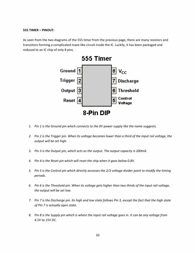
555 TIMER – PINOUT:
As seen from the two diagrams of the 555 timer from the previous page, there are many resistors and
transistors forming a complicated maze-like circuit inside the IC. Luckily, it has been packaged and
reduced to an IC chip of only 8 pins.
1. Pin 1 is the Ground pin which connects to the 0V power supply like the name suggests.
2. Pin 2 is the Trigger pin. When its voltage becomes lower than a third of the input rail voltage, the
output will be set high.
3. Pin 3 is the Output pin, which acts as the output. The output capacity is 200mA.
4. Pin 4 is the Reset pin which will reset the chip when it goes below 0.8V.
5. Pin 5 is the Control pin which directly accesses the 2/3 voltage divider point to modify the timing
periods.
6. Pin 6 is the Threshold pin. When its voltage gets higher than two thirds of the input rail voltage,
the output will be set low.
7. Pin 7 is the Discharge pin. Its high and low state follows Pin 3, except the fact that the high state
of Pin 7 is actually open state.
8. Pin 8 is the Supply pin which is where the input rail voltage goes in. It can be any voltage from
4.5V to 15V DC.

11
555 TIMER – INTERNAL CIRCUITRY IN RELATION TO PINOUT:
As seen from the above basic structure of a 555 timer diagram, on the left are 3 resistors in series. They
are being used as voltage divider resistors so that there can be a one third VCC and two third VCC
voltages into the comparators. These three 5k resistors are where the name 555 timer comes from.
After the resistors are the 2 comparators.
The top comparator compares the Threshold pin voltage with the 2/3 VCC voltage to get an output. Its
output goes high when Threshold is higher than 2/3 VCC, and it goes low when Threshold is lower than
2/3 VCC.
The bottom comparator compares the Trigger pin voltage with the 1/3 VCC voltage to get another
output. Its output goes high when Trigger is lower than 1/3 VCC, and it goes low when Trigger is higher
than 1/3 VCC.
Now these two outputs are put into the flip flop. The top threshold comparator output will go into the
Reset pin of the flip flop. The bottom trigger comparator output will go into the Set pin of the flip flop.
When set is high, the output will be high, when reset is high, the output will be low. If both are low, then
output does not change. If both are high, then it is undefined.
There is a transistor on the bottom after the flip flop. The output of the flip flop is called Q Not. When
Q Not goes high, the transistor turns on, and the discharge voltage of Pin 7 will be pulled down to low
state. When Q Not goes low, the transistor turns off, and Pin 7 is high, or open, to be more precise.

12
Finally, the output Q Not is passed through an inverter to produce the final output of the 555 timer, Q.
Its high low state follows that of the Discharge pin except the fact that its high state is the actual high
state, not just open.
The most important thing to remember from this is when Threshold goes higher than 2/3 VCC, output
goes low and vice versa. When Trigger goes higher than 1/3 VCC, output goes low and vice versa.
555 TIMER – DIFFERENT CONFIGURATIONS:
MONOSTABLE MODE (ONE SHOT):
The 555 timer has different uses depend on how its pins are connected. One configuration of the IC is in
monostable mode, also known as one shot configuration. This is shown below
Monostable Mode (One Shot) 555 Timer Ouput (Monostable Configuration)
In the beginning, the Output pin will be at 0V. So that means the Discharge pin will also be low and will
be pulled to 0V since it follows the output. Now, if we make the Trigger pin low, the output will become
high and this will make the Discharge pin high and open. Next, the capacitor C below Pin 7 will start
charging through the resistor. Eventually this will make the voltage at Pin 6 reach and surpass the
threshold voltage, making the output low again. The Discharge pin will also be low again, which closes
the open circuit and discharges the capacitor through Pin 7. The width of the pulse T generated can be
calculated using the equation:
It can be seen that this monostable configuration can be used as a pulse width modulator. The desired
pulse can be generated using the above equation.

13
BISTABLE MODE (SCHMITT TRIGGER):
The bistable mode, also known as Schmitt trigger is similar to the monostable mode. It acts as a flip flop
with two stable states, high and low. To get a high state output, the Trigger input is simply set low. To
get a low state output, the Reset pin is simply set low.
Bistable Mode (Schmitt Trigger) 555 Timer Output (Bistable Configuration)
ASTABLE MODE:
The astable mode generates an output that, like the name suggests, is unstable. It will change high low
states constantly.
Astable Mode 555 Timer Output (Astable Configuration)
Output Pin (Top) and Capacitor (Bottom)

14
In the beginning, there is no voltage across the capacitor C. As time passes by, it will charge up through
R1 and R2 and continuously increase the voltage at Pin 6 (Threshold) and Pin 2 (Trigger), which are tied
together.
At a certain time, the voltage at Pin 2 will go above 1/3 VCC due to the charging capacitor. This will keep
the output low. After a while, the voltage at Pin 6 will go above 2/3 VCC due to the charging capacitor,
making the output low. This results in Pin 7 being low, so that the capacitor can discharge through R2
and into Pin 7.
The frequency of the output pulse can be calculated using the following formula:
To calculate the time for high state Thigh, use the formula:
( ) ( )
To calculate the time for low state Tlow, use the formula:
( )
This astable mode can be used to generate a pulse wave which is used in this project. This circuit takes
the generated pulse from the capacitor instead of the output because a triangular wave, not square
wave, is needed.

15
Calculations:
Total period T = 0.693*(R1 +2R2)C = 0.693*(1k + 2*50k)*(500pf) = 35ns
Ton = 0.693*(R1+R2)*C = 0.693*(1k+50k)*500pf = 17.7ns
Toff = 0.693*R2*C = 0.693*50k*500pf = 17.3ns
555 TIMER – CONCLUSION:
555 Timer is a very useful IC chip throughout the field. It can be used in LED light blinker, lamp dimmer,
police siren, traffic lights, intruder alarm, motion detector, mobile incoming call indicator, this capstone
project’s switching regulator, and many more applications. There have been billions of 555 timers in
existence to this day, and since it is so easy to use for even beginners, it is known as the gateway to
electronic circuits.

16
SWITCHING REGULATOR – LINEAR vs. SWITCHING:
Once rectified from AC to DC, the current is ready to pass through the regulation component of the
circuit. The purpose of the switching regulator is to regulate and step down the voltage it receives as an
input, much like a buck converter, while providing a highly efficient output as well. In the initial design
stages, two options were available to be incorporated, which were the linear and switching regulators.
The linear regulator is popular in modern day electronics, but lacks in efficiency and power delivery.
While the switching regulator has typical efficiency rates of 85%-97%, its linear counterpart has lower
efficiencies between 14%-40%. Power wasted in the circuit can be calculated with the formula below.
( )
This lower efficiency rate also results in a higher heat dissipation, which requires additional peripheral
components on the circuit, such as heat sinks, cooling fans, and isolation transformers that are bulky
and invasive.
The larger heat dissipation is also a product of the difference between the input and output voltages
being too great, which can be seen in the linear regulators lower efficiency rates. Linear regulators
function by transferring power continuously from the input to an output. A switching regulator, on the
other hand, keeps its efficiency high by breaking up small chunks of energy, bit by bit, and moving them
between the input and output. The inductor and fast-switching diode are responsible for the “switch”
aspect of the switching regulator, hence its coined name.
While linear regulators can power very low powered devices and are cheap to purchase, they are very
inefficient by design. They take the difference between the input and the output, burning it up as heat.
The larger this difference is, the more heat is produced and the more power is wasted in the circuit.
These regulators can waste more power just stepping down the voltage then actually gets delivered to
the output itself. The switching regulator, which delivers energies in bursts, alleviates this fault. These
bursts of energy are controlled by the switching component (inductor/diode) and a controller (555) in
the circuit. The controller regulates the rate at which energy is transferred to the output.

17
SWITCHING REGULATOR – SWITCHING OPERATION:
Because it was known the circuit would be driving an at least 1 Ampere load and a loss of power was not
advantageous, the switching regulator became the preferred choice. Pictured below is a diagram of the
regulation circuit used.
With regards to the controller in this circuit, the 555 timer is responsible for sending pulses to the
comparator (U4 and U5). The regulator relies on a pulse width modulated output that can be controlled
via voltage feedback. Using pulse width modulation controls the average power to the load by
controlling the average voltage it receives.
In the above schematic, D8 is the fast-switching diode and L1 is the inductor component of the buck
converter. When the switch is closed, L1 opposes rising current and generates an electromagnetic field
in its core. The fast-switching diode thus becomes reverse biased. Once current has been established
in the inductor, the switch opens. This current in the inductor causes the current charging in the
adjacant capacitors to rise smoothly. The switch opening is caused by the fast-switching diode that
closes the loop which permits the inductor’s current to keep flowing.
Switch is closed

18
Because the current through the inductor resists change, it must flow through the diode and to the
output. This change in the current causes a step voltage to appear across the inductor. The current
then flows to the higher voltage at Vout. When the switch is open, the inductor’s electromagentic field
discharges and generates a current in the reverse polarity. The fast-switching diode then conducts until
the electromagentic field in the inductor has been depleted.
While there are many and varied ways to step down a voltage between an input and output, a switching
regulator was the optimal choice because it doesn’t incur as many losses in power. Whenever a voltage
source is connected to a capacitor whose initial voltage is not the same as the voltage source, you waste
energy and losses occur.
Alternatively, this loss can be avoided by connecting a voltage source to a current source. An inductor is
the physical element most similar to a current source, which is why it is an important aspect of the
switching regulator. It provides a steady current while stepping down the voltage. Because the current
is reactive and out of phase for the 555 timer’s clock switch as a step down device, it becomes more
efficient.

19
SWITCHING REGULATOR – BUCK CONVERTER CONFIGURATION:
Pictured below is the physical representation of the switching regulator circuit.
This circuit incorporated a 250 uH inductor, F15UP20 fast-switching diode, 2N3904 BJT’s, and a 2N7000
power MOSFET for its regulatory aspect.
As can be observed from above, the circuit utilizes a buck converter configuration to step down the
voltage from 12 V to 8 V. The 555 timer is located on the left section of the board and connects from its
pin 6 to the base of the regulator’s comparator. The buck converter has the inductor connected to the
output of the circuit.
Buck converters use a power MOSFET(2N7000) as a switch that connects and disconnects the input
voltage to the inductor. The inductor acts as a reservoir for every segment of current it receives. Once
the voltage reaches the required level, only the energy necessary for the load is transferred from the
input to the output. Pictured on the next page are the closed and opened states of the buck converter.

20
Once the switch is on, the input voltage connects to the inductor. The difference between the input and
output voltages is then transferred across the inductor, causing its own current to increase.
The current flows into both the load of the circuit and the output capacitor (C2), which begins to charge
the capacitor as well. When the switch is turned off, the input voltage first applied disappears. Because
inductors by nature discharge current steadily over time, the voltage across the inductor will hold the
current constant.
The current through the inductor steps up when the switch is on and steps down when the switch is off.
Usually, the current in the inductor does not drop to zero during operation. Performance is genuinely
better in the continuous mode and it allows maximum output power to be acquired.
Mathematically, VLOn D + VLOf f (1 – D) = 0, where D is the duty cycle.
A fast-switching diode (F15UP20) has a high reverse recovery time and continues to conduct in the
reverse direction because of the stored charges. These diodes become non-conductive much sooner
than their non-fast switching counterparts. The pathway between the anode and the cathode is
somewhat conductive after the current that placed them in that state has disappeared.
The reverse polarity in the diode causes a conductive path in the reverse direction. These diodes act like
capacitors that have been charged, and once a reverse voltage is applied, exerts a current.

21
SWITCHING REGULATOR – MOSFETs & BJTs:
The power MOSFET is fundamental to the switching regulator for a number of reasons. It is unipolar in
nature, which allows it to switch at very high speeds. The only limitation upon the speed is decided by
the transistor’s own internal capacitances. The capacitances must be charged or discharged when the
transistor switches. This can sometimes be a slow affair, as the current that goes through the gate
capacitances is limited by the external circuit. Pictured below is a diagram of the typical power MOSFET.
The CGD capacitance is the connection in series of two
capacitances. The first is COXD, which is created by the
gate electrode, silicon dioxide, and top of the N epitaxial
layer. The other capacitance is CGDJ, caused by the
space-charge zone when the MOSFET is in an off-state.
Controlling the circuit itself can be explained by examining the diagram below.
The switching regulating circuit uses the second pair of BJT’s as a pulse width modulation comparator
from the 555 timer. The first pair are responsible for being the error amplifier. It receives a reference
voltage from the initial 12 V, while the comparator compares the amplified error signal with a waveform
generated across the timing capacitor, C2. The error amplifier output is compared to the voltage from
the 12 V input and energy is then transferred to the buck converter and output of the circuit.

22
CURRENT LIMITER – LINEAR REGULATORS:
As stated in the abstract, the function of current limiting circuitry is to prevent damage to the IC when
an overload is placed on the output of the regulator. In other words, if the load impedance is too low,
such as a short circuit, the regulator would source excessive load current and destroy the pass
transistor.
Every electronic circuit is designed to operate off of some voltage supply, which is assumed to be
constant. A voltage regulator provides this constant DC voltage and with external components,
continuously holds the output voltage at a designed value regardless of changes in load current or input
voltage (as long as the load current and input voltage are within the specified operating range for the
regulator)
The basic linear regulator operates by forcing a fixed voltage to appear at the regulator output terminal.
The control circuitry senses the output voltage, and adjusts the current source according to the load in
order to hold the output voltage at the desired value. A basic linear regulator diagram is shown below.
There are three basic types of linear regulator designs that can maintain a designed output voltage:
Standard (NPN) Regulator, Low Dropout (LDO) Regulator, and Quasi LDO Regulator. The most important
difference between these types as the dropout voltage, which is the minimum voltage drop required
across the regulator to maintain output voltage regulation. A critical point in determining selection of
regulator is that the linear regulator that operates with the smallest voltage across it dissipates the least
internal power, and therefore has the highest efficiency.

23
CURRENT LIMITER – SELECTION OF REGULATOR:
In selecting the best choice for this project, several specifications are evaluated. The major ones include
maximum load current, type of input voltage source, and output voltage precision. The load current that
is needed for this project is a single value, and the regulator selected must be able to provide sufficient
current to the load even under worst-case scenarios.
By the time the input signal reaches the current limiting circuit, it will be a DC voltage. In this case, an
LDO regulator is the best choice because it will utilize the available input voltage more fully. In addition,
LDO regulators allow for greater design flexibility because they offer special features such as load-dump
protection, reverse input voltage protection, error flag, and others. These other features will not be
explored in depth in this project.
The reason for choosing a linear regulator over a switching regulator is because of two protection
circuits found in nearly all ICs: thermal shutdown and current limiting. While the first is not necessarily
needed, as adding a heat sink can be a suitable substitution, the second provides the fundamental core
of this entire current limiter.
The specific IC linear regulator used in this project is the LM317T. This IC is very easy to use, and requires
minimal external circuitry to set regulation. The device itself also includes on-chip current limiting,
thermal overload protection, and safe-operating-are protection.
In terms of meeting specifications, the LM317T can operate with an input voltage of anywhere from 3V
to 37V, and can supply a constant load current of 10mA to 1.5A.

24
CURRENT LIMITER – CONSTANT vs. FOLDBACK:
There are two basic types of current limiting circuits that are most commonly used in linear regulators,
Constant Current Limiting and Voltage-Dependent Current Limiting (sometimes referred to as Foldback
Limiting).
CONSTANT CURRENT LIMITING:
With constant current limiting, the maximum current that the regulator can supply to a load is specified
on its data sheet. Most LDO regulators specify only a single value of maximum current. This value is
guaranteed for any input or output voltage within the operating range for the regulator.
For the simple diagram shown on the previous page, the load current is sensed by the “I SENSE” resistor,
which generates a voltage that is directly related to the current. This voltage is shifted and amplified by
the differential amplifier. The voltage at the output of the differential amplifier is a ground-referenced
signal that is proportional to the load current. This signal is then applied to the inverting input of the
current error amplifier, while a reference voltage is applied to the non-inverting input. The maximum
current limit point occurs when the reference voltage is equal to the voltage at the output of the
differential amplifier.
When load current reaches the limit, the regulator operates in constant current mode. At this point, the
regulator limits the load current to the maximum value, and the output voltage can vary from any value
down to zero volts.
VOLTAGE DEPENDENT (FOLDBACK) CURRENT LIMITING:
This type of current limiting is used by regulators that are high current, greater than 1A. The maximum
load current is dependent on the input-output voltage differential across the IC. This is due to the safe
operating area of transistors, which limits the amount of current a transistor can safely handle as the
voltage increases.

25
In this project, the designed maximum load current is 1A. This means that the load current should never
exceed this value. Due to this specification, constant current limiting is more desirable.
CURRENT LIMITER – OPERATIONAL AMPLIFIER LM741:
In general, the LM741 operational amplifier can be used in many different circuits. They can function as
inverting or non-inverting amplifiers, differentiators or integrators, filters, regulators, peak detectors,
etc. For this project’s purpose, the LM741 will serve as a comparator.
Below is a diagram of the internal circuitry of the LM741.

26
CURRENT LIMITER – LM741 PINOUT:
1. Pin 1 (Offset Null): Since the operational amplifier is the differential type, input offset voltage
must be controlled so as to minimize offset
2. Pin 2 (Inverting Input): All input signals at this pin will be inverted at the output pin
3. Pin 3 (Non-Inverting Input): All input signals at this pin will be process normally without inversion
4. Pin 4 (V-): Negative supply voltage terminal. Operating range for the 741 is -4.5V (minimum) to -
18V (maximum), while specified operating range is between -5V and -15V DC
5. Pin 5 (Offset Null): Same as Pin 1
6. Pin 6 (Output): Output signal’s polarity will be the opposite of the input’s polarity when this
signal is applied to the inverting input
7. Pin 7 (V+): Positive supply voltage terminal. Operating range for the 741 is +4.5V (minimum) to
+18V (maximum), while specified operating range is between +5V and +15V DC.
8. Pin 8 (NC): Stands for “Not Connected”. Nothing connects to this pin

27
CURRENT LIMITER – VARIABLE CURRENT LIMITING CIRCUIT:
This circuit is used to impose a max load current, protecting it from over-current in the case of a short
circuit load. It takes two inputs, a positive 8V DC from the switching voltage regulator, and another -5V
DC from the voltage inverter to power the operational amplifier.
The TIP42 TO-220 package PNP BJT transistor is the only transistor used in this project’s current limiter.
This transistor acts as an on/off switch for determining how much voltage and current to allow at the
load terminals. It takes a small current leaving the base junction and amplifies it at the collector output.
In the event of a short circuit load, the entire input voltage will be dumped across this transistor. This
evaluates to about 64W using the formula below. The TIP42’s power dissipation max rating is 60W, this
transistor must be mounted on a heat sink.
Adjustable current limiting is provided by the operational amplifier LM741, which is used as a
comparator. This IC monitors the voltage across R_SENSE. If this voltage exceeds a certain level, set by
the potentiometer R_LIMIT, the output goes low, dragging down the ADJ pin of the LM317 and thus the
output voltage.
The LED lights up when the load current has reached the limit. Also the potentiometer R21 has one side
connected to -5V instead of 0V so that the output voltage can be varied down to zero volts instead of
the 1.2V limit of the LM317.

28
0.00
0.20
0.40
0.60
0.80
1.00
1.20
0.005.0010.0015.00
Loa
d C
urr
ent
(A)
Load Resistance (Ohms)
CURRENT LIMITER – TESTING:
The current limit is tested by using a load resistance of 10 ohms and lowering it to 1 ohm by 1 ohm
increments. As resistance is decreased, the current should gradually increase until it hits a certain max
limit. Once it hits the maximum load current, the LED lights up, indicating the limit has been reached.
From this point on, any further reduction in load resistance will continue to produce a constant max load
current.
The short-circuit test is performed by replacing the load resistance with a wire. Without a current
limiter, this would result in over-current and the load circuit would be damaged. However, as shown
below, even with a short-circuit the output load current is still under the set maximum limit of 1 A.

29
DIVISION OF LABOR:
ARENDEL RICHARDS
Transformer-Rectifier-Filter
Voltage Inverter
YUN TANG
555 Timer
PETER TU
Current Limiter
JEFFREY WHITE
Switching Regulator
30
REFERENCES:
"555 Timer Circuits." 555 Timer Circuits. 05 May 2013 <http://www.555-timer-circuits.com/>. "555 Timer Circuits." 555 Timer Operating Modes. 05 May 2013 <http://www.555-timer-
circuits.com/operating-modes.html>. "555 timer IC." Wikipedia. 05 May 2013. Wikimedia Foundation. 05 May 2013
<http://en.wikipedia.org/wiki/555_timer_IC>. "The 741 Op-Amp." The 741 Op-Amp. 05 May 2013 <http://www.electronics.dit.ie/staff/mtully/741
tutorial/741 Op-Amp Tutorial.htm>. "A beginner's guide to switching regulators." DimensionEngineering. 05 May 2013
<http://www.dimensionengineering.com/info/switching-regulators>. "Current limiting." Wikipedia. 19 Apr. 2013. Wikimedia Foundation. 05 May 2013
<http://en.wikipedia.org/wiki/Current_limiting>. "Doctronics." 555 timer. 05 May 2013 <http://www.doctronics.co.uk/555.htm>. "Extreme Circuits." Electronics Circuits Diagrams, DIY Electronics Projects, Circuit Schematics. 05 May
2013 <http://www.extremecircuits.net/2010/06/fully-adjustable-power-supply_17.html>. Lager, Aaron. "Use a 555 timer as a switch-mode power supply." EDN. 14 Nov. 2002. 05 May 2013
<http://www.edn.com/design/analog/4345674/Use-a-555-timer-as-a-switch-mode-power-supply>.
"LM317-TI pdf, LM317-TI description, LM317-TI datasheets, LM317-TI view ::: ALLDATASHEET :::."
LM317-TI pdf, LM317-TI description, LM317-TI datasheets, LM317-TI view ::: ALLDATASHEET :::. 05 May 2013 <http://pdf1.alldatasheet.com/datasheet-pdf/view/95600/TI/LM317-TI.html>.
"LM741CN - LM741 Operational Amplifier Datasheet - Buy LM741CN." LM741CN Datasheet. 05 May
2013 <http://www.futurlec.com/Linear/LM741CN.shtml>. "Overclockers." Overclockers. 05 May 2013 <http://www.overclockers.com/understanding-buck-
regulators/>.