Switching Regulator IC Efficiency of Buck Converter -...
16
1/15 www.rohm.co.com December 2016 - Rev.001 © 2016 ROHM Co., Ltd. AEK59-D1-0364-0 Switching Regulator IC Series Efficiency of Buck Converter Switching regulators are known as being highly efficient power sources. To further improve their efficiency, it is helpful to understand the basic mechanism of power loss. This application note explains power loss factors and methods for calculating them. It also explains how the relative importance of power loss factors depends on the specifications of the switching power source. Synchronous rectification type Figure 1 shows the circuit diagram of a synchronous rectification type DC/DC converter. Figure 2 shows the waveforms of the voltage of a switch node and the current waveform of the inductor. The striped patterns represent the areas where the loss occurs. The following nine factors are the main causes of power loss: 1. Conduction loss caused by the on-resistance of the MOSFET ைேு , ைே 2. Switching-loss in the MOSFET ௌௐு , ௌௐ 3. Reverse recovery loss in the body diode ூைா 4. Output capacitance loss in the MOSFET ைௌௌ 5. Dead time loss 6. Gate charge loss in the MOSFET 7. Operation loss caused by the IC control circuit ூ 8. Conduction loss in the inductor ሺோሻ 9. Loss in the capacitor ூே , ை Conduction loss in the MOSFET The conduction loss in the MOSFET is calculated in the A and B sections of the waveform in Figure 2. As the high-side MOSFET is ON and the low-side MOSFET is OFF in the A section, the conduction loss of the high-side MOSFET can be estimated from the output current, on-resistance, and on-duty cycle. As the high-side MOSFET is OFF and the low-side MOSFET is ON in the B section, the conduction loss of the low-side MOSFET can be estimated from the output current, on-resistance, and off-duty cycle. The conduction losses ைேு and ைே are calculated with the following equations. High-side MOSFET ைேு ൌ ܫை ଶ ൈ ைேு ൈ ை ூே ሾሿ Low-side MOSFET ைே ൌ ܫை ଶ ൈ ைே ൈ ൬1 െ ை ூே ൰ ሾሿ ܫை : Output current ሾܣሿ ைேு : High-side MOSFET on-resistance ሾߗሿ ைே : Low-side MOSFET on-resistance ሾߗሿ ூே : Input voltage ሾሿ ை : Output voltage ሾሿ In the equations (1) and (2), the output current is used as the current value. This is the average current of the inductor. As shown in the lower part of Figure 2, greater losses are generated in the actual ramp waveforms. If the current waveform is sharper (peak current is higher), the effective current is obtained by integrating the square of the differential between the peak and bottom values of the current. The loss can then be calculated in more detail. The conduction losses ைேு and ைே are calculated with the following equations. High-side MOSFET ைேு ൌ ቈ ܫை ଶ ሺ ܫ െ ܫ ሻ ଶ 12 ൈ ைேு ൈ ை ூே ሾሿ (1) (2) (3)
Transcript of Switching Regulator IC Efficiency of Buck Converter -...

1/15 www.rohm.co.com December 2016 - Rev.001© 2016 ROHM Co., Ltd. AEK59-D1-0364-0
Switching Regulator IC Series
Efficiency of Buck Converter
Switching regulators are known as being highly efficient power
sources. To further improve their efficiency, it is helpful to
understand the basic mechanism of power loss. This
application note explains power loss factors and methods for
calculating them. It also explains how the relative importance
of power loss factors depends on the specifications of the
switching power source.
Synchronous rectification type
Figure 1 shows the circuit diagram of a synchronous
rectification type DC/DC converter. Figure 2 shows the
waveforms of the voltage of a switch node and the current
waveform of the inductor. The striped patterns represent the
areas where the loss occurs.
The following nine factors are the main causes of power loss:
1. Conduction loss caused by the on-resistance of the
MOSFET ,
2. Switching-loss in the MOSFET ,
3. Reverse recovery loss in the body diode
4. Output capacitance loss in the MOSFET
5. Dead time loss
6. Gate charge loss in the MOSFET
7. Operation loss caused by the IC control circuit
8. Conduction loss in the inductor
9. Loss in the capacitor ,
Conduction loss in the MOSFET
The conduction loss in the MOSFET is calculated in the A and
B sections of the waveform in Figure 2. As the high-side
MOSFET is ON and the low-side MOSFET is OFF in the A
section, the conduction loss of the high-side MOSFET can be
estimated from the output current, on-resistance, and on-duty
cycle. As the high-side MOSFET is OFF and the low-side
MOSFET is ON in the B section, the conduction loss of the
low-side MOSFET can be estimated from the output current,
on-resistance, and off-duty cycle.
The conduction losses and are calculated with
the following equations.
High-side MOSFET
Low-side MOSFET
1
:Output current
:High-side MOSFET on-resistance
:Low-side MOSFET on-resistance
: Input voltage
:Output voltage
In the equations (1) and (2), the output current is used as the
current value. This is the average current of the inductor. As
shown in the lower part of Figure 2, greater losses are
generated in the actual ramp waveforms. If the current
waveform is sharper (peak current is higher), the effective
current is obtained by integrating the square of the differential
between the peak and bottom values of the current. The loss
can then be calculated in more detail.
The conduction losses and are calculated with
the following equations.
High-side MOSFET
12
(1)
(2)
(3)

Application Note
2/15 www.rohm.co.com December 2016 - Rev.001 © 2016 ROHM Co., Ltd.
Efficiency of Buck Converter
AEK59-D1-0364-0
Low-side MOSFET
𝑃𝑃𝑂𝑂𝑂𝑂−𝐿𝐿 = �𝐼𝐼𝑂𝑂𝐶𝐶𝐶𝐶 2 +
(𝐼𝐼𝑃𝑃 − 𝐼𝐼𝑉𝑉)2
12 � × 𝑅𝑅𝑂𝑂𝑂𝑂−𝐿𝐿 × �1 −𝑉𝑉𝑂𝑂𝐶𝐶𝐶𝐶
𝑉𝑉𝐷𝐷𝑂𝑂� [𝑊𝑊]
𝛥𝛥𝐼𝐼𝐿𝐿 =(𝑉𝑉𝐷𝐷𝑂𝑂 − 𝑉𝑉𝑂𝑂𝐶𝐶𝐶𝐶)
𝑓𝑓𝑆𝑆𝑆𝑆 × 𝐿𝐿 ×𝑉𝑉𝑂𝑂𝐶𝐶𝐶𝐶
𝑉𝑉𝐷𝐷𝑂𝑂 [𝐴𝐴]
𝐼𝐼𝑃𝑃 = 𝐼𝐼𝑂𝑂𝐶𝐶𝐶𝐶 +Δ𝐼𝐼𝐿𝐿
2 [𝐴𝐴]
𝐼𝐼𝑃𝑃 = 𝐼𝐼𝑂𝑂𝐶𝐶𝐶𝐶
𝐼𝐼𝑂𝑂𝐶𝐶𝐶𝐶: Output current [𝐴𝐴]
𝐼𝐼𝑃𝑃: Inductor current peak [𝐴𝐴]
𝐼𝐼𝑉𝑉: Inductor current bottom [𝐴𝐴]
𝑅𝑅𝑂𝑂𝑂𝑂−𝐻𝐻: High-side MOSFET on-resistance [𝛺𝛺]
𝑅𝑅𝑂𝑂𝑂𝑂−𝐿𝐿: Low-side MOSFET on-resistance [𝛺𝛺]
𝑉𝑉𝐷𝐷𝑂𝑂: Input voltage [𝑉𝑉]
𝑉𝑉𝑂𝑂𝐶𝐶𝐶𝐶: Output voltage [𝑉𝑉]
𝛥𝛥𝐼𝐼𝐿𝐿: Ripple current of inductor [𝐴𝐴]
𝑓𝑓𝑆𝑆𝑆𝑆: Switching frequency [𝐻𝐻𝐻𝐻]
𝐿𝐿: Inductance value [𝐻𝐻]
Switching-loss in the MOSFET
The switching-losses are calculated in the C and D sections or
in the E and F sections of the waveform in Figure 2. When the
high-side and low-side MOSFETs are turned ON and OFF
alternately, a loss is generated during the transition of the on-
switching. Since the equation for calculating the area of the
two triangles is similar to the equation for calculating the power
losses during the rising and falling transitions, this calculation
can be approximated using a simple geometric equation.
The switching-loss 𝑃𝑃𝑆𝑆𝑆𝑆−𝐻𝐻 is calculated with the following
equation.
High-side MOSFET
𝑃𝑃𝑆𝑆𝑆𝑆−𝐻𝐻 =12
× 𝑉𝑉𝐷𝐷𝑂𝑂 × 𝐼𝐼𝑂𝑂𝐶𝐶𝐶𝐶 × �𝑡𝑡𝑟𝑟−𝐻𝐻 + 𝑡𝑡𝑓𝑓−𝐻𝐻� × 𝑓𝑓𝑆𝑆𝑆𝑆 [𝑊𝑊]
𝑉𝑉𝐷𝐷𝑂𝑂: Input voltage [𝑉𝑉]
𝐼𝐼𝑂𝑂𝐶𝐶𝐶𝐶: Output current [𝐴𝐴]
𝑡𝑡𝑟𝑟−𝐻𝐻: High-side MOSFET rise time [𝑠𝑠𝑠𝑠𝑠𝑠]
𝑡𝑡𝑓𝑓−𝐻𝐻: High-side MOSFET rise time [𝑠𝑠𝑠𝑠𝑠𝑠]
𝑓𝑓𝑆𝑆𝑆𝑆: Switching frequency [𝐻𝐻𝐻𝐻]
When the low-side MOSFET is turned ON by the gate voltage
while the body diode is energized and then the FET is turned
OFF by the gate voltage, the load current continues to flow in
the same direction through the body diode. Therefore, the
drain voltage becomes equal to the forward direction voltage
and remains low. Then, the resulting switching-loss 𝑃𝑃𝑆𝑆𝑆𝑆𝐿𝐿 is
very small, as described in the following equation.
Low-side MOSFET
𝑃𝑃𝑆𝑆𝑆𝑆−𝐿𝐿 =12 × 𝑉𝑉𝐷𝐷 × 𝐼𝐼𝑂𝑂𝐶𝐶𝐶𝐶 × �𝑡𝑡𝑟𝑟−𝐿𝐿 + 𝑡𝑡𝑓𝑓−𝐿𝐿� × 𝑓𝑓𝑆𝑆𝑆𝑆 [𝑊𝑊]
𝑉𝑉𝐷𝐷: Forward direction voltage of
low-side MOSFET body diode [𝑉𝑉]
𝐼𝐼𝑂𝑂𝐶𝐶𝐶𝐶: Output current [𝐴𝐴]
𝑡𝑡𝑟𝑟−𝐿𝐿: Low-side MOSFET rise time [𝑠𝑠𝑠𝑠𝑠𝑠]
𝑡𝑡𝑓𝑓−𝐿𝐿: Low-side MOSFET rise time [𝑠𝑠𝑠𝑠𝑠𝑠]
𝑓𝑓𝑆𝑆𝑆𝑆: Switching frequency [𝐻𝐻𝐻𝐻]
Reverse recovery loss in the body diode
When the high-side MOSFET is turned ON, the transition of
the body diode of the low-side MOSFET from the forward
direction to the reverse bias state causes a diode recovery,
which in turn generates a reverse recovery loss in the body
diode. This loss is determined by the reverse recovery time of
the diode 𝑡𝑡𝐷𝐷𝐷𝐷 . From the reverse recovery properties of the
diode, the loss is calculated with the following equation.
𝑃𝑃𝐷𝐷𝐷𝐷𝑂𝑂𝐷𝐷𝐷𝐷 =12 × 𝑉𝑉𝐷𝐷𝑂𝑂 × 𝐼𝐼𝐷𝐷𝐷𝐷 × 𝑡𝑡𝐷𝐷𝐷𝐷 × 𝑓𝑓𝑆𝑆𝑆𝑆 [𝑊𝑊]
𝑉𝑉𝐷𝐷𝑂𝑂: Input voltage [𝑉𝑉]
𝐼𝐼𝐷𝐷𝐷𝐷: Peak value of
body diode reverse recovery current [𝐴𝐴]
𝑡𝑡𝐷𝐷𝐷𝐷: Body diode reverse recovery time
𝑓𝑓𝑆𝑆𝑆𝑆: Switching frequency [𝐻𝐻𝐻𝐻]
Output capacitance loss in the MOSFET
In each switching cycle, the loss is generated because the
output capacitances of the high-side and low-side MOSFETs
𝐶𝐶𝑂𝑂𝑆𝑆𝑆𝑆 are charged. This loss is calculated with the following
equation.
(5)
(6)
(7)
(4)

Application Note
3/15 www.rohm.co.com December 2016 - Rev.001 © 2016 ROHM Co., Ltd.
Efficiency of Buck Converter
AEK59-D1-0364-0
𝑃𝑃𝐶𝐶𝑂𝑂𝑆𝑆𝑆𝑆 =12 × (𝐶𝐶𝑂𝑂𝑆𝑆𝑆𝑆−𝐿𝐿 + 𝐶𝐶𝑂𝑂𝑆𝑆𝑆𝑆−𝐻𝐻) × 𝑉𝑉𝐷𝐷𝑂𝑂
2 × 𝑓𝑓𝑆𝑆𝑆𝑆 [𝑊𝑊]
𝐶𝐶𝑂𝑂𝑆𝑆𝑆𝑆−𝐿𝐿 = 𝐶𝐶𝐷𝐷𝑆𝑆−𝐿𝐿 + 𝐶𝐶𝐺𝐺𝐷𝐷−𝐿𝐿 [𝐹𝐹]
𝐶𝐶𝑂𝑂𝑆𝑆𝑆𝑆−𝐻𝐻 = 𝐶𝐶𝐷𝐷𝑆𝑆−𝐻𝐻 + 𝐶𝐶𝐺𝐺𝐷𝐷−𝐻𝐻 [𝐹𝐹]
𝐶𝐶𝑂𝑂𝑆𝑆𝑆𝑆−𝐿𝐿: Low-side MOSFET output capacitance [𝐹𝐹]
𝐶𝐶𝐷𝐷𝑆𝑆−𝐿𝐿: Low-side MOSFET drain-source capacitance [𝐹𝐹]
𝐶𝐶𝐺𝐺𝐷𝐷−𝐿𝐿: Low-side MOSFET gate-drain capacitance [𝐹𝐹]
𝐶𝐶𝑂𝑂𝑆𝑆𝑆𝑆−𝐻𝐻: High-side MOSFET output capacitance [𝐹𝐹]
𝐶𝐶𝐷𝐷𝑆𝑆−𝐻𝐻: High-side MOSFET
drain-source capacitance [𝐹𝐹]
𝐶𝐶𝐺𝐺𝐷𝐷−𝐻𝐻: High-side MOSFET gate-drain capacitance [𝐹𝐹]
𝑉𝑉𝐷𝐷𝑂𝑂: Input voltage [𝑉𝑉]
𝑓𝑓𝑆𝑆𝑆𝑆: Switching frequency [𝐻𝐻𝐻𝐻]
Dead time loss
When the high-side and low-side MOSFETs are turned ON
simultaneously, a short circuit occurs between the VIN and
ground, generating a very large current spike. A period of dead
time is provided for turning OFF both of the MOSFETs to
prevent such current spikes from occurring, while the inductor
current continues to flow. During the dead time, this inductor
current flows to the body diode of the low-side MOSFET. The
dead time loss 𝑃𝑃𝐷𝐷 is calculated in the G and H sections of the
waveform in Figure 2 with the following equation.
𝑃𝑃𝐷𝐷 = 𝑉𝑉𝐷𝐷 × 𝐼𝐼𝑂𝑂𝐶𝐶𝐶𝐶 × �𝑡𝑡𝐷𝐷𝑟𝑟 + 𝑡𝑡𝐷𝐷𝑓𝑓� × 𝑓𝑓𝑆𝑆𝑆𝑆 [𝑊𝑊]
𝑉𝑉𝐷𝐷: Forward direction voltage of
low-side MOSFET body diode [𝑉𝑉]
𝐼𝐼𝑂𝑂𝐶𝐶𝐶𝐶: Output current [𝐴𝐴]
𝑡𝑡𝐷𝐷𝑟𝑟: Dead time for rising [𝑠𝑠𝑠𝑠𝑠𝑠]
𝑡𝑡𝐷𝐷𝑓𝑓: Dead time for falling [𝑠𝑠𝑠𝑠𝑠𝑠]
𝑓𝑓𝑆𝑆𝑆𝑆: Switching frequency [𝐻𝐻𝐻𝐻]
Gate charge loss
The Gate charge loss is the power loss caused by charging
the gate of the MOSFET. The gate charge loss depends on
the gate charges (or gate capacitances) of the high-side and
low-side MOSFETs. It is calculated with the following
equations.
𝑃𝑃𝐺𝐺 = �𝑄𝑄𝑔𝑔−𝐻𝐻 + 𝑄𝑄𝑔𝑔−𝐿𝐿� × 𝑉𝑉𝑔𝑔𝑔𝑔 × 𝑓𝑓𝑆𝑆𝑆𝑆 [𝑊𝑊]
or
𝑃𝑃𝐺𝐺 = (𝐶𝐶𝐺𝐺𝑆𝑆−𝐻𝐻 + 𝐶𝐶𝐺𝐺𝑆𝑆−𝐿𝐿) × 𝑉𝑉𝑔𝑔𝑔𝑔 2 × 𝑓𝑓𝑆𝑆𝑆𝑆 [𝑊𝑊]
𝑄𝑄𝑔𝑔−𝐻𝐻: Gate charge of high-side MOSFET [𝐶𝐶]
𝑄𝑄𝑔𝑔−𝐿𝐿: Gate charge of low-side MOSFET [𝐶𝐶]
𝐶𝐶𝐺𝐺𝑆𝑆−𝐻𝐻: Gate capacitance of high-side MOSFET [𝐹𝐹]
𝐶𝐶𝐺𝐺𝑆𝑆−𝐿𝐿: Gate capacitance of low-side MOSFET [𝐹𝐹]
𝑉𝑉𝑔𝑔𝑔𝑔: Gate drive voltage [𝑉𝑉]
𝑓𝑓𝑆𝑆𝑆𝑆: Switching frequency [𝐻𝐻𝐻𝐻]
Operation loss caused by the IC
The consumption power used by the IC control circuit 𝑃𝑃𝐷𝐷𝐶𝐶 is
calculated with the following equation.
𝑃𝑃𝐷𝐷𝐶𝐶 = 𝑉𝑉𝐷𝐷𝑂𝑂 × 𝐼𝐼𝐶𝐶𝐶𝐶 [𝑊𝑊]
𝑉𝑉𝐷𝐷𝑂𝑂: Input voltage [𝑉𝑉]
𝐼𝐼𝐶𝐶𝐶𝐶: IC current consumption [𝐴𝐴]
Conduction loss in the inductor
There are two types of the power loss in the inductor: the
conduction loss caused by the resistance and the core loss
determined by the magnetic properties. Since the calculation
of the core loss is too complex, it is not described in this article.
The conduction loss is generated by the DC resistance (DCR)
of the winding that forms the inductor. The DCR increases as
the wire length increases; on the other hand, it decreases as
the wire cross-section increases. If this trend is applied to the
inductor parts, the DCR increases as the inductance value
increases and decreases as the case size increases.
The conduction loss of the inductor can be estimated with the
following equation. Since the inductor is always energized, it
is not affected by the duty cycle. Since the power loss is
proportional to the square of the current, a higher output
current results in a greater loss. For this reason, it is important
to select the appropriate inductors.
𝑃𝑃𝐿𝐿(𝐷𝐷𝐶𝐶𝐷𝐷) = 𝐼𝐼𝑂𝑂𝐶𝐶𝐶𝐶 2 × DCR [𝑊𝑊]
𝐼𝐼𝑂𝑂𝐶𝐶𝐶𝐶: Output current [𝐴𝐴]
𝐷𝐷𝐶𝐶𝑅𝑅: Inductor direct current resistance [Ω]
Since the output current is used in this equation, the average
current of the inductor is used for the calculation. Similar to the (10)
(11)
(12)
(9)
(13)
(8)

Application Note
4/15 www.rohm.co.com December 2016 - Rev.001 © 2016 ROHM Co., Ltd.
Efficiency of Buck Converter
AEK59-D1-0364-0
above-mentioned calculation for the conduction loss of the
MOSFET, the loss can be calculated in more detail by using
the ramp waveform for the inductor current calculation.
𝑃𝑃𝐿𝐿(𝐷𝐷𝐶𝐶𝐷𝐷) = �𝐼𝐼𝑂𝑂𝐶𝐶𝐶𝐶 2 +
(𝐼𝐼𝑃𝑃 − 𝐼𝐼𝑉𝑉)2
12 � × 𝐷𝐷𝐶𝐶𝑅𝑅 [𝑊𝑊]
𝐼𝐼𝑂𝑂𝐶𝐶𝐶𝐶: Output current [𝐴𝐴]
𝐼𝐼𝑃𝑃: Inductor current peak [𝐴𝐴]
𝐼𝐼𝑉𝑉: Inductor current bottom [𝐴𝐴]
𝐷𝐷𝐶𝐶𝑅𝑅: Inductor direct current resistance [Ω]
Loss in the capacitor
Although several losses are generated in the
capacitor―including series resistance, leakage, and dielectric
loss―these losses are simplified into a general loss model as
equivalent series resistance (ESR). The power loss in the
capacitor is calculated by multiplying the ESR by the square
of the RMS value of the AC current flowing through the
capacitor.
𝑃𝑃𝐶𝐶𝐶𝐶𝑃𝑃(𝐷𝐷𝑆𝑆𝐷𝐷) = 𝐼𝐼𝐶𝐶𝐶𝐶𝑃𝑃(𝐷𝐷𝑅𝑅𝑆𝑆) 2 × 𝐸𝐸𝐸𝐸𝑅𝑅 [𝑊𝑊]
𝐼𝐼𝐶𝐶𝐶𝐶𝑃𝑃(𝐷𝐷𝑅𝑅𝑆𝑆): RMS current of capacitor [𝐴𝐴]
𝐸𝐸𝐸𝐸𝑅𝑅: Equivalent series resistance of capacitor [Ω]
The RMS current in the input capacitor is complex, but it can
be estimated with the following equation.
𝐼𝐼𝐶𝐶𝐷𝐷𝑂𝑂(𝐷𝐷𝑅𝑅𝑆𝑆) = 𝐼𝐼𝑂𝑂𝐶𝐶𝐶𝐶 ×�(𝑉𝑉𝐷𝐷𝑂𝑂 − 𝑉𝑉𝑂𝑂𝐶𝐶𝐶𝐶) × 𝑉𝑉𝑂𝑂𝐶𝐶𝐶𝐶
𝑉𝑉𝐷𝐷𝑂𝑂 [𝐴𝐴]
𝑉𝑉𝐷𝐷𝑂𝑂: Input voltage [𝑉𝑉]
𝑉𝑉𝑂𝑂𝐶𝐶𝐶𝐶: Output voltage [𝑉𝑉]
𝐼𝐼𝑂𝑂𝐶𝐶𝐶𝐶: Output current [𝐴𝐴]
The RMS current in the output capacitor is equal to the RMS
value of the ripple current in the inductor, and calculated with
the following equation.
𝐼𝐼𝐶𝐶𝑂𝑂𝐶𝐶𝐶𝐶(𝐷𝐷𝑅𝑅𝑆𝑆) =𝛥𝛥𝐼𝐼𝐿𝐿
2√3 [𝐴𝐴]
𝛥𝛥𝐼𝐼𝐿𝐿: Ripple current of inductor [𝐴𝐴]
𝛥𝛥𝐼𝐼𝐿𝐿 =(𝑉𝑉𝐷𝐷𝑂𝑂 − 𝑉𝑉𝑂𝑂𝐶𝐶𝐶𝐶)
𝑓𝑓𝑆𝑆𝑆𝑆 × 𝐿𝐿 ×𝑉𝑉𝑂𝑂𝐶𝐶𝐶𝐶
𝑉𝑉𝐷𝐷𝑂𝑂 [𝐴𝐴]
𝑉𝑉𝐷𝐷𝑂𝑂: Input voltage [𝑉𝑉]
𝑉𝑉𝑂𝑂𝐶𝐶𝐶𝐶: Output voltage [𝑉𝑉]
𝑓𝑓𝑆𝑆𝑆𝑆: Switching frequency [𝐻𝐻𝐻𝐻]
𝐿𝐿: Inductance value [𝐻𝐻]
The losses in the input capacitor 𝑃𝑃𝐶𝐶𝐷𝐷𝑂𝑂 and the output
capacitor 𝑃𝑃𝐶𝐶𝑂𝑂𝐶𝐶𝐶𝐶 are calculated by substituting the RMS
current in the equation (15) by those calculated in the
equations (16) and (17), respectively.
Total power loss
The power loss of the IC, P, is obtained by adding all the
losses together.
𝑃𝑃 = 𝑃𝑃𝑂𝑂𝑂𝑂−𝐻𝐻 + 𝑃𝑃𝑂𝑂𝑂𝑂−𝐿𝐿 + 𝑃𝑃𝑆𝑆𝑆𝑆−𝐻𝐻 + 𝑃𝑃𝑆𝑆𝑆𝑆−𝐿𝐿 + 𝑃𝑃𝐷𝐷𝐷𝐷𝑂𝑂𝐷𝐷𝐷𝐷 + 𝑃𝑃𝐶𝐶𝑂𝑂𝑆𝑆𝑆𝑆 +
𝑃𝑃𝐷𝐷 + 𝑃𝑃𝐺𝐺 + 𝑃𝑃𝐷𝐷𝐶𝐶 + 𝑃𝑃𝐿𝐿(𝐷𝐷𝐶𝐶𝐷𝐷) + 𝑃𝑃𝐶𝐶𝐷𝐷𝑂𝑂 + 𝑃𝑃𝐶𝐶𝑂𝑂𝐶𝐶𝐶𝐶 [𝑊𝑊]
𝑃𝑃𝑂𝑂𝑂𝑂−𝐻𝐻: Conduction loss of high-side MOSFET [𝑊𝑊]
𝑃𝑃𝑂𝑂𝑂𝑂−𝐿𝐿: Conduction loss of low-side MOSFET [𝑊𝑊]
𝑃𝑃𝑆𝑆𝑆𝑆−𝐻𝐻: Switching-loss of high-side MOSFET [𝑊𝑊]
𝑃𝑃𝑆𝑆𝑆𝑆−𝐿𝐿: Switching-loss of low-side MOSFET [𝑊𝑊]
𝑃𝑃𝐷𝐷𝐷𝐷𝑂𝑂𝐷𝐷𝐷𝐷: Reverse recovery loss of body diode [𝑊𝑊]
𝑃𝑃𝐶𝐶𝑂𝑂𝑆𝑆𝑆𝑆: Output capacitance loss of MOSFET [𝑊𝑊]
𝑃𝑃𝐷𝐷: Dead time loss [𝑊𝑊]
𝑃𝑃𝐺𝐺: Gate charge loss [𝑊𝑊]
𝑃𝑃𝐷𝐷𝐶𝐶: IC operation loss [𝑊𝑊]
𝑃𝑃𝐿𝐿(𝐷𝐷𝐶𝐶𝐷𝐷): Conduction loss of inductor [𝑊𝑊]
𝑃𝑃𝐶𝐶𝐷𝐷𝑂𝑂: Input capacitor loss [𝑊𝑊]
𝑃𝑃𝐶𝐶𝑂𝑂𝐶𝐶𝐶𝐶: Output capacitor loss [𝑊𝑊]
Efficiency
Since the total power loss is obtained, the efficiency can be
calculated with the following equation.
η=𝑉𝑉𝑂𝑂𝐶𝐶𝐶𝐶 × 𝐼𝐼𝑂𝑂𝐶𝐶𝐶𝐶
𝑉𝑉𝑂𝑂𝐶𝐶𝐶𝐶 × 𝐼𝐼𝑂𝑂𝐶𝐶𝐶𝐶 + 𝑃𝑃
𝑉𝑉𝑂𝑂𝐶𝐶𝐶𝐶: Output voltage [𝑉𝑉]
𝐼𝐼𝑂𝑂𝐶𝐶𝐶𝐶: Output current [𝐴𝐴]
𝑃𝑃: Total power loss [𝑊𝑊]
(19)
(14)
(15)
(16)
(17)
(18)
(20)

Application Note
5/15 www.rohm.co.com December 2016 - Rev.001 © 2016 ROHM Co., Ltd.
Efficiency of Buck Converter
AEK59-D1-0364-0
D
CGS-L
S
G
D
S
G
CGS-H
Controller
ICCVIN
High-side MOSFETRON-H
Low-side MOSFETRON-L
Body-DiodeVD
RLVOUT
IOUT
IL
VSW
FB
RDCRL
COUT
ESR
CGD-H
CGD-L
CDS-H
CDS-L
Figure 1. Circuit diagram of the synchronous rectification type DC/DC converter
tr-H tf-HtONtOFF
tDf tDr
VINVSW
0
IL(AVERAGE)
t
RON-H×IOUT
RON-L×IOUT
Ⓒ Ⓐ Ⓓ Ⓑ
Ⓖ Ⓗ
IP(PEAK)
IV(VALLEY)
Ⓔ Ⓕtr-L tf-L
VD
ΔIL
Figure 2. Switching waveform and loss

Application Note
6/15 www.rohm.co.com December 2016 - Rev.001 © 2016 ROHM Co., Ltd.
Efficiency of Buck Converter
AEK59-D1-0364-0
Calculation example (synchronous rectification type)
Calculation formula Parameters Result
1. Conduction loss
𝑃𝑃𝑂𝑂𝑂𝑂−𝐻𝐻 = �𝐼𝐼𝑂𝑂𝐶𝐶𝐶𝐶 2 +
(𝐼𝐼𝑃𝑃 − 𝐼𝐼𝑉𝑉)2
12 � × 𝑅𝑅𝑂𝑂𝑂𝑂−𝐻𝐻 ×𝑉𝑉𝑂𝑂𝐶𝐶𝐶𝐶
𝑉𝑉𝐷𝐷𝑂𝑂 [𝑊𝑊]
𝑃𝑃𝑂𝑂𝑂𝑂−𝐿𝐿 = �𝐼𝐼𝑂𝑂𝐶𝐶𝐶𝐶 2 +
(𝐼𝐼𝑃𝑃 − 𝐼𝐼𝑉𝑉)2
12 � × 𝑅𝑅𝑂𝑂𝑂𝑂−𝐿𝐿 × �1 −𝑉𝑉𝑂𝑂𝐶𝐶𝐶𝐶
𝑉𝑉𝐷𝐷𝑂𝑂� [𝑊𝑊]
𝛥𝛥𝐼𝐼𝐿𝐿 =(𝑉𝑉𝐷𝐷𝑂𝑂 − 𝑉𝑉𝑂𝑂𝐶𝐶𝐶𝐶)
𝑓𝑓𝑆𝑆𝑆𝑆 × 𝐿𝐿 ×𝑉𝑉𝑂𝑂𝐶𝐶𝐶𝐶
𝑉𝑉𝐷𝐷𝑂𝑂 [𝐴𝐴]
𝐼𝐼𝑃𝑃 = 𝐼𝐼𝑂𝑂𝐶𝐶𝐶𝐶 +Δ𝐼𝐼𝐿𝐿
2 [𝐴𝐴]
𝐼𝐼𝑉𝑉 = 𝐼𝐼𝑂𝑂𝐶𝐶𝐶𝐶 −Δ𝐼𝐼𝐿𝐿
2 [𝐴𝐴]
𝑉𝑉𝐷𝐷𝑂𝑂 ∶ Input voltage 12 𝑉𝑉
𝑉𝑉𝑂𝑂𝐶𝐶𝐶𝐶 ∶ Output voltage 5.0 𝑉𝑉
𝐼𝐼𝑂𝑂𝐶𝐶𝐶𝐶 ∶ Output current 3.0 𝐴𝐴
𝑅𝑅𝑂𝑂𝑂𝑂−𝐻𝐻 ∶ High-side MOSFET on-resistance 100 𝑚𝑚𝛺𝛺
𝑅𝑅𝑂𝑂𝑂𝑂−𝐿𝐿 ∶ Low-side MOSFET on-resistance 70 𝑚𝑚𝛺𝛺
𝐿𝐿 ∶ Inductance value 4.7 𝜇𝜇𝐻𝐻
𝑓𝑓𝑆𝑆𝑆𝑆 ∶ Switching frequency 1.0 𝑀𝑀𝐻𝐻𝐻𝐻
𝑡𝑡𝑟𝑟−𝐻𝐻 ∶ High-side MOSFET rise time 4 𝑛𝑛𝑠𝑠𝑠𝑠𝑠𝑠
𝑡𝑡𝑓𝑓−𝐻𝐻 ∶ High-side MOSFET fall time 6 𝑛𝑛𝑠𝑠𝑠𝑠𝑠𝑠
𝑡𝑡𝑟𝑟−𝐿𝐿 ∶ Low-side MOSFET rise time 2 𝑛𝑛𝑠𝑠𝑠𝑠𝑠𝑠
𝑡𝑡𝑓𝑓−𝐿𝐿 ∶ Low-side MOSFET fall time 2 𝑛𝑛𝑠𝑠𝑠𝑠𝑠𝑠
𝑉𝑉𝐷𝐷 ∶ Forward direction voltage of low-side MOSFET body diode 0.5 𝑉𝑉
𝐼𝐼𝐷𝐷𝐷𝐷 ∶ Peak value of body diode reverse recovery current 0.3 𝐴𝐴
𝑡𝑡𝐷𝐷𝐷𝐷 ∶ Body diode reverse recovery time 25 nsec
𝐶𝐶𝐷𝐷𝑆𝑆−𝐻𝐻 ∶ High-side MOSFET drain-source capacitance 40 𝑝𝑝𝐹𝐹
𝐶𝐶𝐺𝐺𝐷𝐷−𝐻𝐻 ∶ High-side MOSFET gate-drain capacitance 40 𝑝𝑝𝐹𝐹
𝐶𝐶𝐷𝐷𝑆𝑆−𝐿𝐿 ∶ Low-side MOSFET drain-source capacitance 40 𝑝𝑝𝐹𝐹
𝐶𝐶𝐺𝐺𝐷𝐷−𝐿𝐿 ∶ Low-side MOSFET gate-drain capacitance 40 𝑝𝑝𝐹𝐹
𝑡𝑡𝐷𝐷𝑟𝑟 ∶ Dead time for rising 30 𝑛𝑛𝑠𝑠𝑠𝑠𝑠𝑠
𝑡𝑡𝐷𝐷𝑓𝑓 ∶ Dead time for falling 30 𝑛𝑛𝑠𝑠𝑠𝑠𝑠𝑠
𝑄𝑄𝑔𝑔−𝐻𝐻 ∶ Gate charge of high-side MOSFET 1 𝑛𝑛𝐶𝐶
𝑄𝑄𝑔𝑔−𝐿𝐿 ∶ Gate charge of low-side MOSFET 1 𝑛𝑛𝐶𝐶
𝐶𝐶𝐺𝐺𝑆𝑆−𝐻𝐻 ∶ Gate capacitance of high-side MOSFET 200 𝑝𝑝𝐹𝐹
𝐶𝐶𝐺𝐺𝑆𝑆−𝐿𝐿 ∶ Gate capacitance of low-side MOSFET 200 𝑝𝑝𝐹𝐹
𝑉𝑉𝑔𝑔𝑔𝑔 ∶ Gate drive voltage 5.0𝑉𝑉
𝐼𝐼𝐶𝐶𝐶𝐶 ∶ IC current consumption 1.0 𝑚𝑚𝐴𝐴
𝐷𝐷𝐶𝐶𝑅𝑅 ∶ Inductor direct current resistance 80 𝑚𝑚Ω
𝐸𝐸𝐸𝐸𝑅𝑅𝐶𝐶𝐷𝐷𝑂𝑂 ∶ Equivalent series resistance of input capacitor 3 𝑚𝑚𝛺𝛺
𝐸𝐸𝐸𝐸𝑅𝑅𝐶𝐶𝑂𝑂𝐶𝐶𝐶𝐶 ∶ Equivalent series resistance of output capacitor 1 𝑚𝑚𝛺𝛺
376 𝑚𝑚𝑊𝑊 369 𝑚𝑚𝑊𝑊
2. Switching-loss
𝑃𝑃𝑆𝑆𝑆𝑆−𝐻𝐻 =12 × 𝑉𝑉𝐷𝐷𝑂𝑂 × 𝐼𝐼𝑂𝑂𝐶𝐶𝐶𝐶 × �𝑡𝑡𝑟𝑟−𝐻𝐻 + 𝑡𝑡𝑓𝑓−𝐻𝐻� × 𝑓𝑓𝑆𝑆𝑆𝑆 [𝑊𝑊]
𝑃𝑃𝑆𝑆𝑆𝑆−𝐿𝐿 =12 × 𝑉𝑉𝐷𝐷 × 𝐼𝐼𝑂𝑂𝐶𝐶𝐶𝐶 × �𝑡𝑡𝑟𝑟−𝐿𝐿 + 𝑡𝑡𝑓𝑓−𝐿𝐿� × 𝑓𝑓𝑆𝑆𝑆𝑆 [𝑊𝑊]
180 𝑚𝑚𝑊𝑊 3 𝑚𝑚𝑊𝑊
3. Reverse recovery loss
𝑃𝑃𝐷𝐷𝐷𝐷𝑂𝑂𝐷𝐷𝐷𝐷 =12 × 𝑉𝑉𝐷𝐷𝑂𝑂 × 𝐼𝐼𝐷𝐷𝐷𝐷 × 𝑡𝑡𝐷𝐷𝐷𝐷 × 𝑓𝑓𝑆𝑆𝑆𝑆 [𝑊𝑊]
45 𝑚𝑚𝑊𝑊
4. Output capacitance loss in the MOSFET
𝑃𝑃𝐶𝐶𝑂𝑂𝑆𝑆𝑆𝑆 =12 × (𝐶𝐶𝑂𝑂𝑆𝑆𝑆𝑆−𝐿𝐿 + 𝐶𝐶𝑂𝑂𝑆𝑆𝑆𝑆−𝐻𝐻) × 𝑉𝑉𝐷𝐷𝑂𝑂
2 × 𝑓𝑓𝑆𝑆𝑆𝑆 [𝑊𝑊]
𝐶𝐶𝑂𝑂𝑆𝑆𝑆𝑆−𝐿𝐿 = 𝐶𝐶𝐷𝐷𝑆𝑆−𝐿𝐿 + 𝐶𝐶𝐺𝐺𝐷𝐷−𝐿𝐿 [𝐹𝐹]
𝐶𝐶𝑂𝑂𝑆𝑆𝑆𝑆−𝐻𝐻 = 𝐶𝐶𝐷𝐷𝑆𝑆−𝐻𝐻 + 𝐶𝐶𝐺𝐺𝐷𝐷−𝐻𝐻 [𝐹𝐹]
11.5 𝑚𝑚𝑊𝑊
5. Dead time loss
𝑃𝑃𝐷𝐷 = 𝑉𝑉𝐷𝐷 × 𝐼𝐼𝑂𝑂𝐶𝐶𝐶𝐶 × �𝑡𝑡𝐷𝐷𝑟𝑟 + 𝑡𝑡𝐷𝐷𝑓𝑓� × 𝑓𝑓𝑆𝑆𝑆𝑆 [𝑊𝑊] 90 𝑚𝑚𝑊𝑊
6. Gate charge loss
𝑃𝑃𝐺𝐺 = �𝑄𝑄𝑔𝑔−𝐻𝐻 + 𝑄𝑄𝑔𝑔−𝐿𝐿� × 𝑉𝑉𝑔𝑔𝑔𝑔 × 𝑓𝑓𝑆𝑆𝑆𝑆
or
𝑃𝑃𝐺𝐺 = (𝐶𝐶𝐺𝐺𝑆𝑆−𝐻𝐻 + 𝐶𝐶𝐺𝐺𝑆𝑆−𝐿𝐿) × 𝑉𝑉𝑔𝑔𝑔𝑔 2 × 𝑓𝑓𝑆𝑆𝑆𝑆
10 𝑚𝑚𝑊𝑊
7. Operation loss caused by the IC
𝑃𝑃𝐷𝐷𝐶𝐶 = 𝑉𝑉𝐷𝐷𝑂𝑂 × 𝐼𝐼𝐶𝐶𝐶𝐶 12 𝑚𝑚𝑊𝑊
8. Conduction loss in the inductor
𝑃𝑃𝐿𝐿(𝐷𝐷𝐶𝐶𝐷𝐷) = �𝐼𝐼𝑂𝑂𝐶𝐶𝐶𝐶 2 +
(𝐼𝐼𝑃𝑃 − 𝐼𝐼𝑉𝑉)2
12 � × 𝐷𝐷𝐶𝐶𝑅𝑅 [𝑊𝑊] 723 𝑚𝑚𝑊𝑊
Application Note
7/15 www.rohm.co.com December 2016 - Rev.001 © 2016 ROHM Co., Ltd.
Efficiency of Buck Converter
AEK59-D1-0364-0
Calculation example (synchronous rectification type) continued
Calculation formula Parameters Result
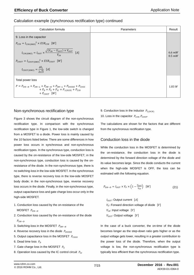
9. Loss in the capacitor
𝑃𝑃𝐶𝐶𝐷𝐷𝑂𝑂 = 𝐼𝐼𝐶𝐶𝐷𝐷𝑂𝑂(𝐷𝐷𝑅𝑅𝑆𝑆) 2 × 𝐸𝐸𝐸𝐸𝑅𝑅𝐶𝐶𝐷𝐷𝑂𝑂 [𝑊𝑊]
𝐼𝐼𝐶𝐶𝐷𝐷𝑂𝑂(𝐷𝐷𝑅𝑅𝑆𝑆) = 𝐼𝐼𝑂𝑂𝐶𝐶𝐶𝐶 ×�(𝑉𝑉𝐷𝐷𝑂𝑂 − 𝑉𝑉𝑂𝑂𝐶𝐶𝐶𝐶) × 𝑉𝑉𝑂𝑂𝐶𝐶𝐶𝐶
𝑉𝑉𝐷𝐷𝑂𝑂 [𝐴𝐴]
𝑃𝑃𝐶𝐶𝑂𝑂𝐶𝐶𝐶𝐶 = 𝐼𝐼𝐶𝐶𝑂𝑂𝐶𝐶𝐶𝐶(𝐷𝐷𝑅𝑅𝑆𝑆) 2 × 𝐸𝐸𝐸𝐸𝑅𝑅𝐶𝐶𝑂𝑂𝐶𝐶𝐶𝐶 [𝑊𝑊]
𝐼𝐼𝐶𝐶𝑂𝑂𝐶𝐶𝐶𝐶(𝐷𝐷𝑅𝑅𝑆𝑆) =𝛥𝛥𝐼𝐼𝐿𝐿
2√3 [𝐴𝐴]
6.6 𝑚𝑚𝑊𝑊 0.5 𝑚𝑚𝑊𝑊
Total power loss
𝑃𝑃 = 𝑃𝑃𝑂𝑂𝑂𝑂−𝐻𝐻 + 𝑃𝑃𝑂𝑂𝑂𝑂−𝐿𝐿 + 𝑃𝑃𝑆𝑆𝑆𝑆−𝐻𝐻 + 𝑃𝑃𝑆𝑆𝑆𝑆−𝐿𝐿 + 𝑃𝑃𝐷𝐷𝐷𝐷𝑂𝑂𝐷𝐷𝐷𝐷 + 𝑃𝑃𝐶𝐶𝑂𝑂𝑆𝑆𝑆𝑆+ 𝑃𝑃𝐷𝐷 + 𝑃𝑃𝐺𝐺 + 𝑃𝑃𝐷𝐷𝐶𝐶 + 𝑃𝑃𝐿𝐿(𝐷𝐷𝐶𝐶𝐷𝐷) + 𝑃𝑃𝐶𝐶𝐷𝐷𝑂𝑂+ 𝑃𝑃𝐶𝐶𝑂𝑂𝐶𝐶𝐶𝐶 [𝑊𝑊]
1.83 𝑊𝑊
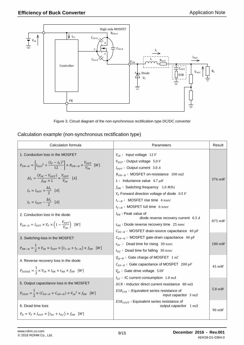
Non-synchronous rectification type
Figure 3 shows the circuit diagram of the non-synchronous
rectification type. In comparison with the synchronous
rectification type in Figure 1, the low-side switch is changed
from a MOSFET to a diode. Power loss is mainly caused by
the 10 factors listed below. There are some differences in how
power loss occurs in synchronous and non-synchronous
rectification types. In the synchronous type, conduction loss is
caused by the on-resistance of the low-side MOSFET; in the
non-synchronous type, conduction loss is caused by the on-
resistance of the diode. In the non-synchronous type, there is
no switching-loss in the low-side MOSFET. In the synchronous
type, there is reverse recovery loss in the low-side MOSFET
body diode; in the non-synchronous type, reverse recovery
loss occurs in the diode. Finally, in the non-synchronous type,
output capacitance loss and gate charge loss occur only in the
high-side MOSFET.
1. Conduction loss caused by the on-resistance of the
MOSFET 𝑃𝑃𝑂𝑂𝑂𝑂−𝐻𝐻
2. Conduction loss caused by the on-resistance of the diode
𝑃𝑃𝑂𝑂𝑂𝑂−𝐷𝐷
3. Switching-loss in the MOSFET 𝑃𝑃𝑆𝑆𝑆𝑆−𝐻𝐻
4. Reverse recovery loss in the diode 𝑃𝑃𝐷𝐷𝐷𝐷𝑂𝑂𝐷𝐷𝐷𝐷
5. Output capacitance loss in the MOSFET 𝑃𝑃𝐶𝐶𝑂𝑂𝑆𝑆𝑆𝑆
6. Dead time loss 𝑃𝑃𝐷𝐷
7. Gate charge loss in the MOSFET 𝑃𝑃𝐺𝐺
8. Operation loss caused by the IC control circuit 𝑃𝑃𝐷𝐷𝐶𝐶
9. Conduction loss in the inductor 𝑃𝑃𝐿𝐿(𝐷𝐷𝐶𝐶𝐷𝐷)
10. Loss in the capacitor 𝑃𝑃𝐶𝐶𝐷𝐷𝑂𝑂, 𝑃𝑃𝐶𝐶𝑂𝑂𝐶𝐶𝐶𝐶
The calculations are shown for the factors that are different
from the synchronous rectification type.
Conduction loss in the diode
While the conduction loss in the MOSFET is determined by
the on-resistance, the conduction loss in the diode is
determined by the forward direction voltage of the diode and
its value becomes large. Since the diode conducts the current
when the high-side MOSFET is OFF, the loss can be
estimated with the following equation.
𝑃𝑃𝑂𝑂𝑂𝑂−𝐷𝐷 = 𝐼𝐼𝑂𝑂𝐶𝐶𝐶𝐶 × 𝑉𝑉𝐹𝐹 × �1 − 𝑉𝑉𝑂𝑂𝑂𝑂𝑂𝑂
𝑉𝑉𝐼𝐼𝐼𝐼� [𝑊𝑊]
𝐼𝐼𝑂𝑂𝐶𝐶𝐶𝐶: Output current [𝐴𝐴]
𝑉𝑉𝐹𝐹: Forward direction voltage of diode [𝑉𝑉]
𝑉𝑉𝐷𝐷𝑂𝑂: Input voltage [𝑉𝑉]
𝑉𝑉𝑂𝑂𝐶𝐶𝐶𝐶: Output voltage [𝑉𝑉]
In the case of a buck converter, the on-time of the diode
becomes longer as the step-down ratio gets higher or as the
output voltage gets lower, resulting in a greater contribution to
the power loss of the diode. Therefore, when the output
voltage is low, the non-synchronous rectification type is
typically less efficient than the synchronous rectification type.
(21)

Application Note
8/15 www.rohm.co.com December 2016 - Rev.001 © 2016 ROHM Co., Ltd.
Efficiency of Buck Converter
AEK59-D1-0364-0
Reverse recovery loss in the diode
The reverse recovery loss in the diode is calculated in the
same way as for the body diode of the low-side MOSFET in
the synchronous rectification type. When the MOSFET is
turned ON, the transition from the forward direction to the
reverse bias state of the diode causes a diode recovery,
generating a reverse recovery loss in the diode. This loss is
determined by the reverse recovery time of the diode 𝑡𝑡𝐷𝐷𝐷𝐷 .
From the reverse recovery properties of the diode, the loss is
calculated with the following equation.
𝑃𝑃𝐷𝐷𝐷𝐷𝑂𝑂𝐷𝐷𝐷𝐷 =12 × 𝑉𝑉𝐷𝐷𝑂𝑂 × 𝐼𝐼𝐷𝐷𝐷𝐷 × 𝑡𝑡𝐷𝐷𝐷𝐷 × 𝑓𝑓𝑆𝑆𝑆𝑆 [𝑊𝑊]
𝑉𝑉𝐷𝐷𝑂𝑂: Input voltage [𝑉𝑉]
𝐼𝐼𝐷𝐷𝐷𝐷: Peak value of diode reverse recovery current [𝐴𝐴]
𝑡𝑡𝐷𝐷𝐷𝐷: Diode reverse recovery time [𝑠𝑠𝑠𝑠𝑠𝑠]
𝑓𝑓𝑆𝑆𝑆𝑆: Switching frequency [𝐻𝐻𝐻𝐻]
Output capacitance loss in the MOSFET
In each switching cycle, a loss is generated because the
output capacitance of the MOSFET 𝐶𝐶𝑂𝑂𝑆𝑆𝑆𝑆 is charged. This loss
can be estimated with the following equation.
𝑃𝑃𝐶𝐶𝑂𝑂𝑆𝑆𝑆𝑆 =12 × (𝐶𝐶𝐷𝐷𝑆𝑆−𝐻𝐻 + 𝐶𝐶𝐺𝐺𝐷𝐷−𝐻𝐻) × 𝑉𝑉𝐷𝐷𝑂𝑂
2 × 𝑓𝑓𝑆𝑆𝑆𝑆 [𝑊𝑊]
𝐶𝐶𝐷𝐷𝑆𝑆−𝐻𝐻: MOSFET drain-source capacitance [𝐹𝐹]
𝐶𝐶𝐺𝐺𝐷𝐷−𝐻𝐻: MOSFET gate-drain capacitance [𝐹𝐹]
𝑉𝑉𝐷𝐷𝑂𝑂: Input voltage [𝑉𝑉]
𝑓𝑓𝑆𝑆𝑆𝑆: Switching frequency [𝐻𝐻𝐻𝐻]
Gate charge loss
The Gate charge loss is the power loss caused by charging
the gate of the MOSFET. The gate charge loss depends on
the gate charge (or gate capacitance) of the MOSFET and is
calculated with the following equations.
𝑃𝑃𝐺𝐺 = 𝑄𝑄𝑔𝑔−𝐻𝐻 × 𝑉𝑉𝑔𝑔𝑔𝑔 × 𝑓𝑓𝑆𝑆𝑆𝑆 [𝑊𝑊]
or
𝑃𝑃𝐺𝐺 = 𝐶𝐶𝐺𝐺𝑆𝑆−𝐻𝐻 × 𝑉𝑉𝑔𝑔𝑔𝑔 2 × 𝑓𝑓𝑆𝑆𝑆𝑆 [𝑊𝑊]
𝑄𝑄𝑔𝑔−𝐻𝐻: Gate charge of MOSFET [𝐶𝐶]
𝐶𝐶𝐺𝐺𝑆𝑆−𝐻𝐻: Gate capacitance of MOSFET [𝐹𝐹]
𝑉𝑉𝑔𝑔𝑔𝑔: Gate drive voltage [𝑉𝑉]
𝑓𝑓𝑆𝑆𝑆𝑆: Switching frequency [𝐻𝐻𝐻𝐻]
Total power loss
The power loss of the IC, P, is obtained by adding all the
losses together.
𝑃𝑃 = 𝑃𝑃𝑂𝑂𝑂𝑂−𝐻𝐻 + 𝑃𝑃𝑂𝑂𝑂𝑂−𝐷𝐷 + 𝑃𝑃𝑆𝑆𝑆𝑆−𝐻𝐻 + 𝑃𝑃𝐷𝐷𝐷𝐷𝑂𝑂𝐷𝐷𝐷𝐷 + 𝑃𝑃𝐶𝐶𝑂𝑂𝑆𝑆𝑆𝑆 + 𝑃𝑃𝐷𝐷 + 𝑃𝑃𝐺𝐺 +
𝑃𝑃𝐷𝐷𝐶𝐶 + 𝑃𝑃𝐿𝐿(𝐷𝐷𝐶𝐶𝐷𝐷) + 𝑃𝑃𝐶𝐶𝐷𝐷𝑂𝑂 + 𝑃𝑃𝐶𝐶𝑂𝑂𝐶𝐶𝐶𝐶 [𝑊𝑊]
𝑃𝑃𝑂𝑂𝑂𝑂−𝐻𝐻: Conduction loss of MOSFET [𝑊𝑊]
𝑃𝑃𝑂𝑂𝑂𝑂−𝐷𝐷: Conduction loss caused by
on-resistance of diode [𝑊𝑊]
𝑃𝑃𝑆𝑆𝑆𝑆−𝐻𝐻: Switching-loss of MOSFET [𝑊𝑊]
𝑃𝑃𝐷𝐷𝐷𝐷𝑂𝑂𝐷𝐷𝐷𝐷: Reverse recovery loss of diode [𝑊𝑊]
𝑃𝑃𝐶𝐶𝑂𝑂𝑆𝑆𝑆𝑆: Output capacitance loss of MOSFET [𝑊𝑊]
𝑃𝑃𝐷𝐷: Dead time loss [𝑊𝑊]
𝑃𝑃𝐺𝐺: Gate charge loss of MOSFET [𝑊𝑊]
𝑃𝑃𝐷𝐷𝐶𝐶: IC operation loss [𝑊𝑊] 𝑃𝑃𝐿𝐿(𝐷𝐷𝐶𝐶𝐷𝐷): Conduction loss of inductor [𝑊𝑊]
𝑃𝑃𝐶𝐶𝐷𝐷𝑂𝑂: Input capacitor loss [𝑊𝑊]
𝑃𝑃𝐶𝐶𝑂𝑂𝐶𝐶𝐶𝐶: Output capacitor loss [𝑊𝑊]
(22)
(23)
(26)
(24)
(25)
Application Note
9/15 www.rohm.co.com December 2016 - Rev.001 © 2016 ROHM Co., Ltd.
Efficiency of Buck Converter
AEK59-D1-0364-0
D
S
G
CGS-H
Controller
ICCVIN
High-side MOSFETRON-H
DiodeVF
RLVOUT
IOUT
IL
VSW
FB
RDCRL
COUT
ESR
CGD-H
CDS-H
Figure 3. Circuit diagram of the non-synchronous rectification type DC/DC converter
Calculation example (non-synchronous rectification type)
Calculation formula Parameters Result
1. Conduction loss in the MOSFET
𝑃𝑃𝑂𝑂𝑂𝑂−𝐻𝐻 = �𝐼𝐼𝑂𝑂𝐶𝐶𝐶𝐶 2 +
(𝐼𝐼𝑃𝑃 − 𝐼𝐼𝑉𝑉)2
12 � × 𝑅𝑅𝑂𝑂𝑂𝑂−𝐻𝐻 ×𝑉𝑉𝑂𝑂𝐶𝐶𝐶𝐶
𝑉𝑉𝐷𝐷𝑂𝑂 [𝑊𝑊]
𝛥𝛥𝐼𝐼𝐿𝐿 =(𝑉𝑉𝐷𝐷𝑂𝑂 − 𝑉𝑉𝑂𝑂𝐶𝐶𝐶𝐶)
𝑓𝑓𝑆𝑆𝑆𝑆 × 𝐿𝐿 ×𝑉𝑉𝑂𝑂𝐶𝐶𝐶𝐶
𝑉𝑉𝐷𝐷𝑂𝑂 [𝐴𝐴]
𝐼𝐼𝑃𝑃 = 𝐼𝐼𝑂𝑂𝐶𝐶𝐶𝐶 +Δ𝐼𝐼𝐿𝐿
2 [𝐴𝐴]
𝐼𝐼𝑉𝑉 = 𝐼𝐼𝑂𝑂𝐶𝐶𝐶𝐶 −Δ𝐼𝐼𝐿𝐿
2 [𝐴𝐴]
𝑉𝑉𝐷𝐷𝑂𝑂 ∶ Input voltage 12 𝑉𝑉
𝑉𝑉𝑂𝑂𝐶𝐶𝐶𝐶 ∶ Output voltage 5.0 𝑉𝑉
𝐼𝐼𝑂𝑂𝐶𝐶𝐶𝐶 ∶ Output current 3.0 𝐴𝐴
𝑅𝑅𝑂𝑂𝑂𝑂−𝐻𝐻 ∶ MOSFET on-resistance 100 𝑚𝑚𝛺𝛺
𝐿𝐿 ∶ Inductance value 4.7 𝜇𝜇𝐻𝐻
𝑓𝑓𝑆𝑆𝑆𝑆 ∶ Switching frequency 1.0 𝑀𝑀𝐻𝐻𝐻𝐻
𝑉𝑉𝐹𝐹 Forward direction voltage of diode 0.5 𝑉𝑉
𝑡𝑡𝑟𝑟−𝐻𝐻 ∶ MOSFET rise time 4 𝑛𝑛𝑠𝑠𝑠𝑠𝑠𝑠
𝑡𝑡𝑓𝑓−𝐻𝐻 ∶ MOSFET fall time 6 𝑛𝑛𝑠𝑠𝑠𝑠𝑠𝑠
𝐼𝐼𝐷𝐷𝐷𝐷 ∶ Peak value of diode reverse recovery current 0.3 𝐴𝐴
𝑡𝑡𝐷𝐷𝐷𝐷 ∶ Diode reverse recovery time 25 nsec
𝐶𝐶𝐷𝐷𝑆𝑆−𝐻𝐻 ∶ MOSFET drain-source capacitance 40 pF
𝐶𝐶𝐺𝐺𝐷𝐷−𝐻𝐻 ∶ MOSFET gate-drain capacitance 40 pF
𝑡𝑡𝐷𝐷𝑟𝑟 ∶ Dead time for rising 30 𝑛𝑛𝑠𝑠𝑠𝑠𝑠𝑠
𝑡𝑡𝐷𝐷𝑓𝑓 ∶ Dead time for falling 30 𝑛𝑛𝑠𝑠𝑠𝑠𝑠𝑠
𝑄𝑄𝑔𝑔−𝐻𝐻 ∶ Gate charge of MOSFET 1 𝑛𝑛𝐶𝐶
𝐶𝐶𝐺𝐺𝑆𝑆−𝐻𝐻 ∶ Gate capacitance of MOSFET 200 𝑝𝑝𝐹𝐹
𝑉𝑉𝑔𝑔𝑔𝑔 ∶ Gate drive voltage 5.0𝑉𝑉
𝐼𝐼𝐶𝐶𝐶𝐶 ∶ IC current consumption 1.0 𝑚𝑚𝐴𝐴
𝐷𝐷𝐶𝐶𝑅𝑅 ∶ Inductor direct current resistance 80 𝑚𝑚Ω
𝐸𝐸𝐸𝐸𝑅𝑅𝐶𝐶𝐷𝐷𝑂𝑂 ∶ :Equivalent series resistance of input capacitor 3 𝑚𝑚𝛺𝛺
𝐸𝐸𝐸𝐸𝑅𝑅𝐶𝐶𝑂𝑂𝐶𝐶𝐶𝐶 ∶ Equivalent series resistance of output capacitor 1 𝑚𝑚𝛺𝛺
376 𝑚𝑚𝑊𝑊
2. Conduction loss in the diode
𝑃𝑃𝑂𝑂𝑂𝑂−𝐷𝐷 = 𝐼𝐼𝑂𝑂𝐶𝐶𝐶𝐶 × 𝑉𝑉𝐹𝐹 × �1 −𝑉𝑉𝑂𝑂𝐶𝐶𝐶𝐶
𝑉𝑉𝐷𝐷𝑂𝑂� [𝑊𝑊]
875 𝑚𝑚𝑊𝑊
3. Switching-loss in the MOSFET
𝑃𝑃𝑆𝑆𝑆𝑆−𝐻𝐻 =12 × 𝑉𝑉𝐷𝐷𝑂𝑂 × 𝐼𝐼𝑂𝑂𝐶𝐶𝐶𝐶 × �𝑡𝑡𝑟𝑟−𝐻𝐻 + 𝑡𝑡𝑓𝑓−𝐻𝐻� × 𝑓𝑓𝑆𝑆𝑆𝑆 [𝑊𝑊]
180 𝑚𝑚𝑊𝑊
4. Reverse recovery loss in the diode
𝑃𝑃𝐷𝐷𝐷𝐷𝑂𝑂𝐷𝐷𝐷𝐷 =12 × 𝑉𝑉𝐷𝐷𝑂𝑂 × 𝐼𝐼𝐷𝐷𝐷𝐷 × 𝑡𝑡𝐷𝐷𝐷𝐷 × 𝑓𝑓𝑆𝑆𝑆𝑆 [𝑊𝑊]
45 𝑚𝑚𝑊𝑊
5. Output capacitance loss in the MOSFET
𝑃𝑃𝐶𝐶𝑂𝑂𝑆𝑆𝑆𝑆 =12 × (𝐶𝐶𝐷𝐷𝑆𝑆−𝐻𝐻 + 𝐶𝐶𝐺𝐺𝐷𝐷−𝐻𝐻) × 𝑉𝑉𝐷𝐷𝑂𝑂
2 × 𝑓𝑓𝑆𝑆𝑆𝑆 [𝑊𝑊] 5.8 𝑚𝑚𝑊𝑊
6. Dead time loss
𝑃𝑃𝐷𝐷 = 𝑉𝑉𝐹𝐹 × 𝐼𝐼𝑂𝑂𝐶𝐶𝐶𝐶 × �𝑡𝑡𝐷𝐷𝑟𝑟 + 𝑡𝑡𝐷𝐷𝑓𝑓� × 𝑓𝑓𝑆𝑆𝑆𝑆 [𝑊𝑊] 90 𝑚𝑚𝑊𝑊

Application Note
10/15 www.rohm.co.com December 2016 - Rev.001 © 2016 ROHM Co., Ltd.
Efficiency of Buck Converter
AEK59-D1-0364-0
Calculation example (non-synchronous rectification type) continued
Calculation formula Parameters Result
7. Gate charge loss
𝑃𝑃𝐺𝐺 = 𝑄𝑄𝑔𝑔−𝐻𝐻 × 𝑉𝑉𝑔𝑔𝑔𝑔 × 𝑓𝑓𝑆𝑆𝑆𝑆
or
𝑃𝑃𝐺𝐺 = 𝐶𝐶𝐺𝐺𝑆𝑆−𝐻𝐻 × 𝑉𝑉𝑔𝑔𝑔𝑔 2 × 𝑓𝑓𝑆𝑆𝑆𝑆
5 𝑚𝑚𝑊𝑊
8. Operation loss caused by the IC
𝑃𝑃𝐷𝐷𝐶𝐶 = 𝑉𝑉𝐷𝐷𝑂𝑂 × 𝐼𝐼𝐶𝐶𝐶𝐶 12 𝑚𝑚𝑊𝑊
9. Conduction loss in the inductor
𝑃𝑃𝐿𝐿(𝐷𝐷𝐶𝐶𝐷𝐷) = �𝐼𝐼𝑂𝑂𝐶𝐶𝐶𝐶 2 +
(𝐼𝐼𝑃𝑃 − 𝐼𝐼𝑉𝑉)2
12 � × 𝐷𝐷𝐶𝐶𝑅𝑅 [𝑊𝑊] 723 𝑚𝑚𝑊𝑊
10. Loss in the capacitor
𝑃𝑃𝐶𝐶𝐷𝐷𝑂𝑂 = 𝐼𝐼𝐶𝐶𝐷𝐷𝑂𝑂(𝐷𝐷𝑅𝑅𝑆𝑆) 2 × 𝐸𝐸𝐸𝐸𝑅𝑅𝐶𝐶𝐷𝐷𝑂𝑂 [𝑊𝑊]
𝐼𝐼𝐶𝐶𝐷𝐷𝑂𝑂(𝐷𝐷𝑅𝑅𝑆𝑆) = 𝐼𝐼𝑂𝑂𝐶𝐶𝐶𝐶 ×�(𝑉𝑉𝐷𝐷𝑂𝑂 − 𝑉𝑉𝑂𝑂𝐶𝐶𝐶𝐶) × 𝑉𝑉𝑂𝑂𝐶𝐶𝐶𝐶
𝑉𝑉𝐷𝐷𝑂𝑂 [𝐴𝐴]
𝑃𝑃𝐶𝐶𝑂𝑂𝐶𝐶𝐶𝐶 = 𝐼𝐼𝐶𝐶𝑂𝑂𝐶𝐶𝐶𝐶(𝐷𝐷𝑅𝑅𝑆𝑆) 2 × 𝐸𝐸𝐸𝐸𝑅𝑅𝐶𝐶𝑂𝑂𝐶𝐶𝐶𝐶 [𝑊𝑊]
𝐼𝐼𝐶𝐶𝑂𝑂𝐶𝐶𝐶𝐶(𝐷𝐷𝑅𝑅𝑆𝑆) =𝛥𝛥𝐼𝐼𝐿𝐿
2√3 [𝐴𝐴]
6.6 𝑚𝑚𝑊𝑊 0.5 𝑚𝑚𝑊𝑊
Total power loss
𝑃𝑃 = 𝑃𝑃𝑂𝑂𝑂𝑂−𝐻𝐻 + 𝑃𝑃𝑂𝑂𝑂𝑂−𝐷𝐷 + 𝑃𝑃𝑆𝑆𝑆𝑆−𝐻𝐻 + 𝑃𝑃𝐷𝐷𝐷𝐷𝑂𝑂𝐷𝐷𝐷𝐷 + 𝑃𝑃𝐶𝐶𝑂𝑂𝑆𝑆𝑆𝑆 + 𝑃𝑃𝐷𝐷 + 𝑃𝑃𝐺𝐺+ 𝑃𝑃𝐷𝐷𝐶𝐶 + 𝑃𝑃𝐿𝐿(𝐷𝐷𝐶𝐶𝐷𝐷) + 𝑃𝑃𝐶𝐶𝐷𝐷𝑂𝑂 + 𝑃𝑃𝐶𝐶𝑂𝑂𝐶𝐶𝐶𝐶 [𝑊𝑊]
2.32 𝑊𝑊
Loss factor
Here we follow how the relative importance of the power loss
factors depends on the specification of the switching power
source.
Figure 4 shows the behavior when the output current is varied
in the synchronous rectification type. When the current is high,
the conduction losses in the MOSFET and the inductor play
major roles. This is because the power loss is proportional to
the square of the current, as shown in the equations (3), (4),
and (14). These losses can be reduced by using MOSFETs
with a low on-resistance and by selecting inductors with a low
DCR. Since parts with lower conduction resistance are
generally larger in size, this selection is a trade-off between
conduction loss and size. In addition, the parasitic capacitance
describe below typically increases as the MOSFET size
increases, causing another trade-off. At low currents, there is
a greater impact from the switching-loss in the MOSFET, the
output capacitance loss in the MOSFET, the gate charge loss
in the MOSFET, and the operation loss of the IC. These
MOSFET-related losses are affected mainly by the parasitic
capacitance values based on the equations (5), (8), (10), and
(11). Although the capacitance value and the loss can be
reduced by using a smaller MOSFET, the current capability is
also reduced in general, causing a trade-off between the
output current value and the size. In addition, since these
values are proportional to the switching frequency, the method
to reduce the loss by lowering the switching frequency is
commonly applied when the current is low. The operation loss
caused of the IC can be reduced by optimizing the circuit
current in the control circuit.
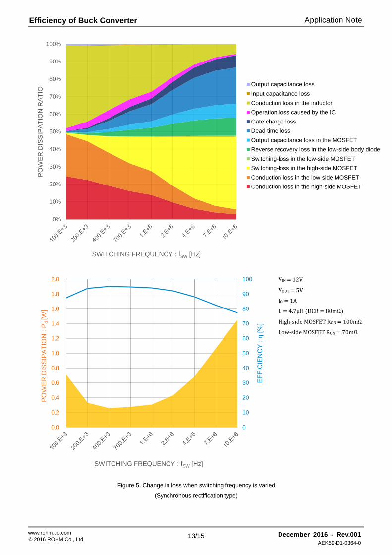
Figure 5 shows the behavior when the switching frequency is

Application Note
11/15 www.rohm.co.com December 2016 - Rev.001 © 2016 ROHM Co., Ltd.
Efficiency of Buck Converter
AEK59-D1-0364-0
varied in the synchronous rectification type. When operating
at high speed, there are increases in the switching-loss in the
MOSFET, the reverse recovery loss of the body diode of the
MOSFET, the output capacitance loss in the MOSFET, and the
dead time loss. Since these MOSFET-related losses increase
in proportion to the switching frequency as shown in the
equations (5), (7), and (8), it is necessary to select an element
that has a low capacitance and that performs switching
operations at high speed. As mentioned above, although the
capacitance value and the loss can be reduced by using a
smaller MOSFET, the current capability is also reduced in
general, causing a trade-off between the output current value
and the size. To reduce the dead time loss, it is necessary to
shorten the dead time by using a design that operates the
control circuit at high speed—i.e., by combining the control
circuit with a MOSFET that can operate at high speed.
Figure 6 shows the behavior when the output voltage is varied
in the synchronous rectification type. This figure illustrates the
change in the duty ratio of the switching. To make it easier to
understand, the input voltage is set to 10 V, resulting in duty
ratios of 10% and 20% for output voltages of 1 V and 2 V,
respectively. It is shown that the on-time of the low-side
MOSFET becomes longer with a lower duty ratio, increasing
the conduction loss in the low-side MOSFET, while the on-time
of the high-side MOSFET becomes longer with a higher-duty
ratio, increasing the conduction loss in the high-side MOSFET.
Figure 7 shows the same behavior as in Figure 6, with the
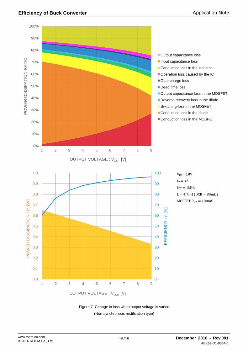
converter replaced by a non-synchronous type. In comparison
with the synchronous type in Figure 6, the conduction loss is
greater in the diode that corresponds to the low-side MOSFET
in the synchronous type. It is also shown that, when the duty
ratio is higher, the difference in the loss between the
synchronous and non-synchronous rectification types is
smaller, since the on-time of the high-side MOSFET becomes
longer. Also, loss in the non-synchronous type become greater
as the duty ratio decreases, since the diode on-time becomes
longer. To reduce such loss, it is necessary to select parts with
diodes that have a lower forward direction voltage.
Application Note
12/15 www.rohm.co.com December 2016 - Rev.001 © 2016 ROHM Co., Ltd.
Efficiency of Buck Converter
AEK59-D1-0364-0
0%
10%
20%
30%
40%
50%
60%
70%
80%
90%
100%
0.1 0.2 0.4 0.7 1 2 4 7 10
POW
ER D
ISSI
PATI
ON
RAT
IO
OUTPUT CURRENT : IOUT [A]
出力コンデンサの損失
入力コンデンサの損失
インダクタの伝導損失
ICの動作損失
ゲート電荷損失
デッドタイム損失
MOSFET出力容量損失
ローサイドボディーダイオード逆回復損失
ローサイドMOSFET スイッチイング損失
ハイサイドMOSFET スイッチング損失
ローサイドMOSFET 伝導損失
ハイサイドMOSFET 伝導損失
0
10
20
30
40
50
60
70
80
90
100
0
2
4
6
8
10
12
14
16
18
20
0.1 0.2 0.4 0.7 1 2 4 7 10
EFFI
CIE
NC
Y : η
[%]
POW
ER D
ISSI
PATI
ON
: P d
[W]
OUTPUT CURRENT : IOUT [A]
Figure 4. Change in loss when output current is varied
(Synchronous rectification type)
VIN = 12V
VOUT = 5V
fSW = 1MHz
L = 4.7μH (DCR = 80mΩ)
High-side MOSFET RON = 100mΩ
Low-side MOSFET RON = 70mΩ
Output capacitance loss Input capacitance loss Conduction loss in the inductor Operation loss caused by the IC Gate charge loss Dead time loss Output capacitance loss in the MOSFET Reverse recovery loss in the low-side body diode Switching-loss in the low-side MOSFET Switching-loss in the high-side MOSFET Conduction loss in the low-side MOSFET Conduction loss in the high-side MOSFET
Application Note
13/15 www.rohm.co.com December 2016 - Rev.001 © 2016 ROHM Co., Ltd.
Efficiency of Buck Converter
AEK59-D1-0364-0
0%
10%
20%
30%
40%
50%
60%
70%
80%
90%
100%PO
WER
DIS
SIPA
TIO
N R
ATIO
SWITCHING FREQUENCY : fSW [Hz]
出力コンデンサの損失
入力コンデンサの損失
インダクタの伝導損失
ICの動作損失
ゲート電荷損失
デッドタイム損失
MOSFET出力容量損失
ローサイドボディーダイオード逆回復損失
ローサイドMOSFET スイッチイング損失
ハイサイドMOSFET スイッチング損失
ローサイドMOSFET 伝導損失
ハイサイドMOSFET 伝導損失
0
10
20
30
40
50
60
70
80
90
100
0.0
0.2
0.4
0.6
0.8
1.0
1.2
1.4
1.6
1.8
2.0
EFFI
CIE
NC
Y : η
[%]
POW
ER D
ISSI
PATI
ON
: P d
[W]
SWITCHING FREQUENCY : fSW [Hz]
Figure 5. Change in loss when switching frequency is varied
(Synchronous rectification type)
VIN = 12V
VOUT = 5V
IO = 1A
L = 4.7μH (DCR = 80mΩ)
High-side MOSFET RON = 100mΩ
Low-side MOSFET RON = 70mΩ
Output capacitance loss Input capacitance loss Conduction loss in the inductor Operation loss caused by the IC Gate charge loss Dead time loss Output capacitance loss in the MOSFET Reverse recovery loss in the low-side body diode Switching-loss in the low-side MOSFET Switching-loss in the high-side MOSFET Conduction loss in the low-side MOSFET Conduction loss in the high-side MOSFET

Application Note
14/15 www.rohm.co.com December 2016 - Rev.001 © 2016 ROHM Co., Ltd.
Efficiency of Buck Converter
AEK59-D1-0364-0
0%
10%
20%
30%
40%
50%
60%
70%
80%
90%
100%
1 2 3 4 5 6 7 8 9
POW
ER D
ISSI
PATI
ON
RAT
IO
OUTPUT VOLTAGE : VOUT [V]
出力コンデンサの損失
入力コンデンサの損失
インダクタの伝導損失
ICの動作損失
ゲート電荷損失
デッドタイム損失
MOSFET出力容量損失
ローサイドボディーダイオード逆回復損失
ローサイドMOSFET スイッチイング損失
ハイサイドMOSFET スイッチング損失
ローサイドMOSFET 伝導損失
ハイサイドMOSFET 伝導損失
0
10
20
30
40
50
60
70
80
90
100
0.0
0.1
0.2
0.3
0.4
0.5
0.6
0.7
0.8
0.9
1.0
1 2 3 4 5 6 7 8 9
EFFI
CIE
NC
Y : η
[%]
POW
ER D
ISSI
PATI
ON
: P d
[W]
OUTPUT VOLTAGE : VOUT [V]
Figure 6. Change in loss when output voltage is varied
(Synchronous rectification type)
VIN = 10V
IO = 1A
fSW = 1MHz
L = 4.7μH (DCR = 80mΩ)
High-side MOSFET RON = 100mΩ
Low-side MOSFET RON = 70mΩ
Output capacitance loss Input capacitance loss Conduction loss in the inductor Operation loss caused by the IC Gate charge loss Dead time loss Output capacitance loss in the MOSFET Reverse recovery loss in the low-side body diode Switching-loss in the low-side MOSFET Switching-loss in the high-side MOSFET Conduction loss in the low-side MOSFET Conduction loss in the high-side MOSFET
Application Note
15/15 www.rohm.co.com December 2016 - Rev.001 © 2016 ROHM Co., Ltd.
Efficiency of Buck Converter
AEK59-D1-0364-0
0%
10%
20%
30%
40%
50%
60%
70%
80%
90%
100%
1 2 3 4 5 6 7 8 9
POW
ER D
ISSI
PATI
ON
RAT
IO
OUTPUT VOLTAGE : VOUT [V]
出力コンデンサの損失
入力コンデンサの損失
インダクタの伝導損失
ICの動作損失
ゲート電荷損失
デッドタイム損失
MOSFET出力容量損失
ダイオード逆回復損失
MOSFET スイッチング損失
ダイオード 伝導損失
MOSFET 伝導損失
0
10
20
30
40
50
60
70
80
90
100
0.0
0.1
0.2
0.3
0.4
0.5
0.6
0.7
0.8
0.9
1.0
1 2 3 4 5 6 7 8 9
EFFI
CIE
NC
Y : η
[%]
POW
ER D
ISSI
PATI
ON
: P d
[W]
OUTPUT VOLTAGE : VOUT [V]
Figure 7. Change in loss when output voltage is varied
(Non-synchronous rectification type)
VIN = 10V
IO = 1A
fSW = 1MHz
L = 4.7μH (DCR = 80mΩ)
MOSFET RON = 100mΩ
Output capacitance loss
Input capacitance loss
Conduction loss in the inductor
Operation loss caused by the IC
Gate charge loss
Dead time loss
Output capacitance loss in the MOSFET
Reverse recovery loss in the diode
Switching-loss in the MOSFET
Conduction loss in the diode Conduction loss in the MOSFET

R1102Awww.rohm.com© 2016 ROHM Co., Ltd. All rights reserved.
Notice
ROHM Customer Support System http://www.rohm.com/contact/
Thank you for your accessing to ROHM product informations. More detail product informations and catalogs are available, please contact us.
N o t e s
The information contained herein is subject to change without notice.
Before you use our Products, please contact our sales representative and verify the latest specifica-tions :
Although ROHM is continuously working to improve product reliability and quality, semicon-ductors can break down and malfunction due to various factors.Therefore, in order to prevent personal injury or fire arising from failure, please take safety measures such as complying with the derating characteristics, implementing redundant and fire prevention designs, and utilizing backups and fail-safe procedures. ROHM shall have no responsibility for any damages arising out of the use of our Poducts beyond the rating specified by ROHM.
Examples of application circuits, circuit constants and any other information contained herein are provided only to illustrate the standard usage and operations of the Products. The peripheral conditions must be taken into account when designing circuits for mass production.
The technical information specified herein is intended only to show the typical functions of and examples of application circuits for the Products. ROHM does not grant you, explicitly or implicitly, any license to use or exercise intellectual property or other rights held by ROHM or any other parties. ROHM shall have no responsibility whatsoever for any dispute arising out of the use of such technical information.
The Products are intended for use in general electronic equipment (i.e. AV/OA devices, communi-cation, consumer systems, gaming/entertainment sets) as well as the applications indicated in this document.
The Products specified in this document are not designed to be radiation tolerant.
For use of our Products in applications requiring a high degree of reliability (as exemplified below), please contact and consult with a ROHM representative : transportation equipment (i.e. cars, ships, trains), primary communication equipment, traffic lights, fire/crime prevention, safety equipment, medical systems, servers, solar cells, and power transmission systems.
Do not use our Products in applications requiring extremely high reliability, such as aerospace equipment, nuclear power control systems, and submarine repeaters.
ROHM shall have no responsibility for any damages or injury arising from non-compliance with the recommended usage conditions and specifications contained herein.
ROHM has used reasonable care to ensure the accuracy of the information contained in this document. However, ROHM does not warrants that such information is error-free, and ROHM shall have no responsibility for any damages arising from any inaccuracy or misprint of such information.
Please use the Products in accordance with any applicable environmental laws and regulations, such as the RoHS Directive. For more details, including RoHS compatibility, please contact a ROHM sales office. ROHM shall have no responsibility for any damages or losses resulting non-compliance with any applicable laws or regulations.
When providing our Products and technologies contained in this document to other countries, you must abide by the procedures and provisions stipulated in all applicable export laws and regulations, including without limitation the US Export Administration Regulations and the Foreign Exchange and Foreign Trade Act.
This document, in part or in whole, may not be reprinted or reproduced without prior consent of ROHM.
1)
2)
3)
4)
5)
6)
7)
8)
9)
10)
11)
12)
13)
14)