Switching algebra and logic gates
47
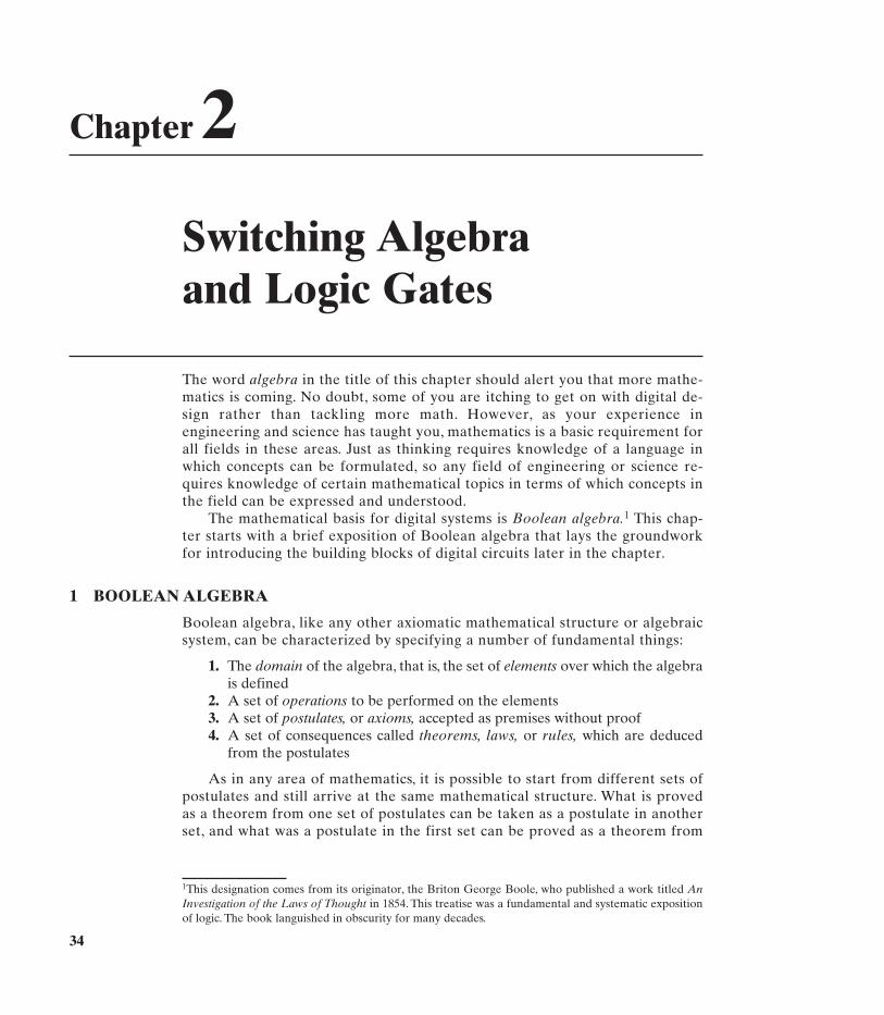
34 Chapter 2 Switching Algebra and Logic Gates The word algebra in the title of this chapter should alert you that more mathe- matics is coming. No doubt, some of you are itching to get on with digital de- sign rather than tackling more math. However, as your experience in engineering and science has taught you, mathematics is a basic requirement for all fields in these areas. Just as thinking requires knowledge of a language in which concepts can be formulated, so any field of engineering or science re- quires knowledge of certain mathematical topics in terms of which concepts in the field can be expressed and understood. The mathematical basis for digital systems is Boolean algebra. 1 This chap- ter starts with a brief exposition of Boolean algebra that lays the groundwork for introducing the building blocks of digital circuits later in the chapter. 1 BOOLEAN ALGEBRA Boolean algebra, like any other axiomatic mathematical structure or algebraic system, can be characterized by specifying a number of fundamental things: 1. The domain of the algebra, that is, the set of elements over which the algebra is defined 2. A set of operations to be performed on the elements 3. A set of postulates, or axioms, accepted as premises without proof 4. A set of consequences called theorems, laws, or rules, which are deduced from the postulates As in any area of mathematics, it is possible to start from different sets of postulates and still arrive at the same mathematical structure. What is proved as a theorem from one set of postulates can be taken as a postulate in another set, and what was a postulate in the first set can be proved as a theorem from 1 This designation comes from its originator, the Briton George Boole, who published a work titled An Investigation of the Laws of Thought in 1854. This treatise was a fundamental and systematic exposition of logic. The book languished in obscurity for many decades.
-
Upload
tarun-gehlot -
Category
Documents
-
view
1.104 -
download
5
Transcript of Switching algebra and logic gates
34
Chapter 2
Switching Algebraand Logic Gates
The word algebra in the title of this chapter should alert you that more mathe-matics is coming. No doubt, some of you are itching to get on with digital de-sign rather than tackling more math. However, as your experience inengineering and science has taught you, mathematics is a basic requirement forall fields in these areas. Just as thinking requires knowledge of a language inwhich concepts can be formulated, so any field of engineering or science re-quires knowledge of certain mathematical topics in terms of which concepts inthe field can be expressed and understood.
The mathematical basis for digital systems is Boolean algebra.1 This chap-ter starts with a brief exposition of Boolean algebra that lays the groundworkfor introducing the building blocks of digital circuits later in the chapter.
1 BOOLEAN ALGEBRA
Boolean algebra, like any other axiomatic mathematical structure or algebraicsystem, can be characterized by specifying a number of fundamental things:
1. The domain of the algebra, that is, the set of elements over which the algebrais defined
2. A set of operations to be performed on the elements3. A set of postulates, or axioms, accepted as premises without proof4. A set of consequences called theorems, laws, or rules, which are deduced
from the postulates
As in any area of mathematics, it is possible to start from different sets ofpostulates and still arrive at the same mathematical structure. What is provedas a theorem from one set of postulates can be taken as a postulate in anotherset, and what was a postulate in the first set can be proved as a theorem from
1This designation comes from its originator, the Briton George Boole, who published a work titled AnInvestigation of the Laws of Thought in 1854. This treatise was a fundamental and systematic expositionof logic. The book languished in obscurity for many decades.
Boolean Algebra 35
another set of postulates. So how do we decide on postulates? Clearly, one re-quirement for a set of postulates is consistency. It would not do for the conse-quences of one postulate to contradict those of another. Another requirementoften stated is independence. However, independence involves the customaryobjective of ending up with a minimal set of postulates that still permits the de-rivation of all of the theorems. So long as a mathematical rule is consistent withthe others, it can be added as a postulate without harm. If it is dependent on theprevious postulates, however, the added rule is derivable from them and soneed not be taken as a postulate.
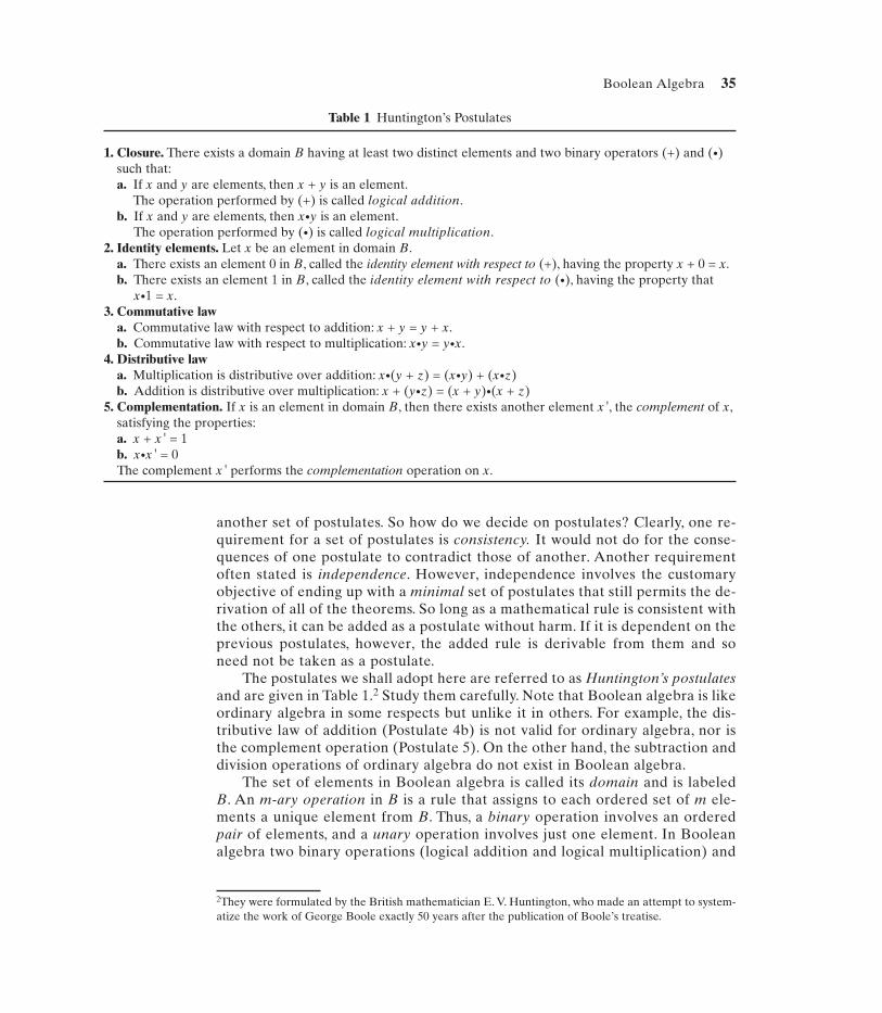
The postulates we shall adopt here are referred to as Huntington’s postulatesand are given in Table 1.2 Study them carefully. Note that Boolean algebra is likeordinary algebra in some respects but unlike it in others. For example, the dis-tributive law of addition (Postulate 4b) is not valid for ordinary algebra, nor isthe complement operation (Postulate 5). On the other hand, the subtraction anddivision operations of ordinary algebra do not exist in Boolean algebra.
The set of elements in Boolean algebra is called its domain and is labeledB. An m-ary operation in B is a rule that assigns to each ordered set of m ele-ments a unique element from B. Thus, a binary operation involves an orderedpair of elements, and a unary operation involves just one element. In Booleanalgebra two binary operations (logical addition and logical multiplication) and
2They were formulated by the British mathematician E. V. Huntington, who made an attempt to system-atize the work of George Boole exactly 50 years after the publication of Boole’s treatise.
Table 1 Huntington’s Postulates
1. Closure. There exists a domain B having at least two distinct elements and two binary operators (+) and (•)such that:a. If x and y are elements, then x + y is an element.
The operation performed by (+) is called logical addition.b. If x and y are elements, then x•y is an element.
The operation performed by (•) is called logical multiplication.2. Identity elements. Let x be an element in domain B.
a. There exists an element 0 in B, called the identity element with respect to (+), having the property x + 0 = x.b. There exists an element 1 in B, called the identity element with respect to (•), having the property that
x•1 = x.3. Commutative law
a. Commutative law with respect to addition: x + y = y + x.b. Commutative law with respect to multiplication: x•y = y•x.
4. Distributive lawa. Multiplication is distributive over addition: x•(y + z) = (x•y) + (x•z)b. Addition is distributive over multiplication: x + (y•z) = (x + y)•(x + z)
5. Complementation. If x is an element in domain B, then there exists another element x', the complement of x,satisfying the properties:a. x + x' = 1 b. x•x' = 0The complement x' performs the complementation operation on x.
one unary operation (complementation) are defined. Many Boolean algebraswith different sets of elements can exist. The terminology Boolean algebra is ageneric way of referring to them all.
Duality Principle
An examination of Huntington’s postulates reveals a certain symmetry: thepostulates come in pairs. One of the postulates in each pair can be obtainedfrom the other one
• By interchanging the two binary operators, and • By interchanging the two identity elements when they appear explicitly.
Thus, one of the commutative laws can be obtained from the other by inter-changing the operators (+) and (•). The same is true of the two distributive laws.Consequently, whatever results can be deduced from the postulates should re-main valid if
• The operators (+) and (•) are interchanged, and • The identity elements 0 and 1 are interchanged.
This property of Boolean algebra is referred to as the duality principle.Whenever some result (theorem) is deduced from the postulates, the dualityprinciple can be invoked as proof of the dual theorem.
Fundamental Theorems
We will now establish a number of consequences (theorems, rules, or laws) thatfollow from Huntington’s postulates and from the duality principle. The proofswill be carried out step by step, with explicit justification for each step given byreferring to the appropriate postulate or previously proved theorem. Two of thegeneral methods of proof used in mathematics are
• Proof by contradiction• Proof by the principle of (mathematical) induction
A proof by contradiction proceeds by assuming that the opposite of the de-sired result is true, and then deducing from this assumption a result that con-tradicts an already-known truth. This means that the opposite of the desiredresult is not true; therefore, the desired result itself must be true.
A proof by the principle of induction proceeds as follows. A propositionP(i) is claimed to be true for all integers i. To prove the claim, it is necessary todo two things:
• Prove that the claim is true for some small integer, say i = 1.• Assume it to be true for an arbitrary integer k and then show that it must,
therefore, be true for the next integer, k + 1.
The latter step means that since the result is true for i = 1, it must be true forthe next integer i = 2 (1 + 1); then it must be true for i = 3 (2 + 1); and so on forall other integers.
36 Chapter 2 Switching Algebra and Logic Gates
Boolean Algebra 37
Another general method of proof, which is discussed in the next subsection,is especially valid for a Boolean algebra with only two elements.
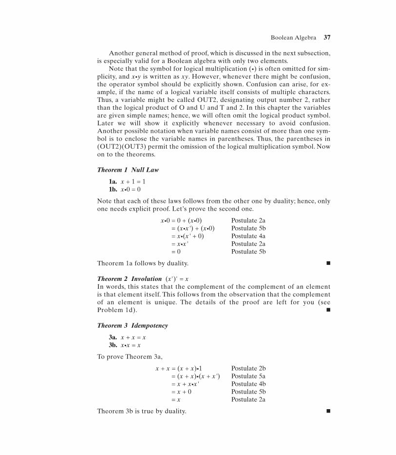
Note that the symbol for logical multiplication (•) is often omitted for sim-plicity, and x•y is written as xy. However, whenever there might be confusion,the operator symbol should be explicitly shown. Confusion can arise, for ex-ample, if the name of a logical variable itself consists of multiple characters.Thus, a variable might be called OUT2, designating output number 2, ratherthan the logical product of O and U and T and 2. In this chapter the variablesare given simple names; hence, we will often omit the logical product symbol.Later we will show it explicitly whenever necessary to avoid confusion.Another possible notation when variable names consist of more than one sym-bol is to enclose the variable names in parentheses. Thus, the parentheses in(OUT2)(OUT3) permit the omission of the logical multiplication symbol. Nowon to the theorems.
Theorem 1 Null Law
1a. x + 1 = 11b. x•0 = 0
Note that each of these laws follows from the other one by duality; hence, onlyone needs explicit proof. Let’s prove the second one.
x•0 = 0 + (x•0) Postulate 2a= (x•x') + (x•0) Postulate 5b= x•(x' + 0) Postulate 4a= x•x' Postulate 2a= 0 Postulate 5b
Theorem 1a follows by duality. �
Theorem 2 Involution (x')' = xIn words, this states that the complement of the complement of an elementis that element itself. This follows from the observation that the complementof an element is unique. The details of the proof are left for you (seeProblem 1d). �
Theorem 3 Idempotency
3a. x + x = x3b. x•x = x
To prove Theorem 3a,
x + x = (x + x)•1 Postulate 2b= (x + x)•(x + x') Postulate 5a= x + x•x' Postulate 4b= x + 0 Postulate 5b= x Postulate 2a
Theorem 3b is true by duality. �
38 Chapter 2 Switching Algebra and Logic Gates
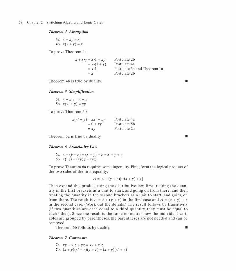
Theorem 4 Absorption
4a. x + xy = x4b. x(x + y) = x
To prove Theorem 4a,
x + x•y = x•1 + xy Postulate 2b= x•(1 + y) Postulate 4a= x•1 Postulate 3a and Theorem 1a= x Postulate 2b
Theorem 4b is true by duality. �
Theorem 5 Simplification
5a. x + x'y = x + y5b. x(x' + y) = xy
To prove Theorem 5b,
x(x' + y) = xx' + xy Postulate 4a= 0 + xy Postulate 5b= xy Postulate 2a
Theorem 5a is true by duality. �
Theorem 6 Associative Law
6a. x + (y + z) = (x + y) + z = x + y + z6b. x(yz) = (xy)z = xyz
To prove Theorem 6a requires some ingenuity. First, form the logical product ofthe two sides of the first equality:
A = [x + (y + z)]•[(x + y) + z]
Then expand this product using the distributive law, first treating the quan-tity in the first brackets as a unit to start, and going on from there; and thentreating the quantity in the second brackets as a unit to start, and going onfrom there. The result is A = x + (y + z) in the first case and A = (x + y) + zin the second case. (Work out the details.) The result follows by transitivity(if two quantities are each equal to a third quantity, they must be equal toeach other). Since the result is the same no matter how the individual vari-ables are grouped by parentheses, the parentheses are not needed and can beremoved.
Theorem 6b follows by duality. �
Theorem 7 Consensus
7a. xy + x'z + yz = xy + x'z7b. (x + y)(x' + z)(y + z) = (x + y)(x' + z)
Boolean Algebra 39
To prove Theorem 7a,
xy + x'z + yz = xy + x'z + yz(x + x') Postulate 5a= xy + x'z + yzx + yzx' Postulate 4a= (xy + xyz) + (x'z + x'zy) Postulate 3b and Theorem 6a= xy + x'z Theorem 4a
Theorem 7b is true by duality. �
Theorem 8 De Morgan’s Law
8a. (x + y)' = x'y'8b. (xy)' = x' + y'
Prove Theorem 8a by showing that x'y' satisfies both conditions in Postulate 5 ofbeing the complement of x + y.
Condition 1
(x + y) + x'y' = (x + x'y') + y Postulate 3a and Theorem 6a= (x + y') + y Theorem 5a= x + (y' + y) Theorem 6a= x + 1 Postulate 5a= 1 Theorem 1a
Condition 2
(x + y)(x'y') = xx'y' + yx'y' Postulates 3b and 4a= 0•y' + x'(yy') Postulates 5b and 3b= 0 Postulates 5b and Theorem 1b
Theorem 8b is true by duality. �
A number of other important results are left for you to prove in the prob-lem set, but we will use them here as if proved. They include the following:
1. The identity elements 0 and 1 are distinct elements.2. The identity elements are unique.3. The inverse of an element is unique.
Exercise 1 Prove that each identity element is the complement of the other one.�
Switching Algebra
For the Boolean algebra discussed so far in this book, the domain has not beenrestricted. That is, no limitation has been placed on the number of elements inthe Boolean algebra. From Huntington’s postulates, we know that in everyBoolean algebra there are two specific elements: the identity elements. Hence,any Boolean algebra has at least two elements. In this book, let us henceforthlimit ourselves to a two-element Boolean algebra.3
3It is possible to prove that the number of elements in any Boolean algebra is some power of 2: 2n, for n ≥ 1.
40 Chapter 2 Switching Algebra and Logic Gates
In a 1937 paper, Claude Shannon implemented a two-element Boolean al-gebra with a circuit of switches.4 Now a switch is a device that can be placed ineither one of two stable positions: off or on. These positions can just as well bedesignated 0 and 1 (or the reverse). For this reason, two-element Boolean al-gebra has been called switching algebra. The identity elements themselves arecalled the switching constants. Similarly, any variables that represent the switch-ing constants are called switching variables.
This explains some of the common terminology used in this area, but we havealready used some terminology whose source is not evident. The terms logicalmultiplication and logical addition were introduced in the first of Huntington’spostulates. To explain where the adjective logical comes from, we will have to di-gress slightly.
Over the centuries a number of different algebraic systems have been de-veloped in different contexts. The language used in describing each system andthe operations carried out in that system made sense in the context in which thealgebra was developed. The algebra of sets is one of these; another is a systemcalled propositional logic, which was developed in the study of philosophy.
It is possible for different algebraic systems, arising from different con-texts, to have similar properties. This possibility is the basis for the followingdefinition.
Two algebraic systems are said to be isomorphic if they can be madeidentical by changing the names of the elements and the names and symbolsused to designate the operations.
Propositional logic is concerned with simple propositions—whether or notthey are true or false, how the simple propositions can be combined into morecomplex propositions, and how the truth or falsity of the complex propositionscan be deduced from the truth or falsity of the simple ones. A simple proposi-tion is a declarative statement that may be either true or false, but not both. Itis said to have two possible truth values: true (T) or false (F). Examples are
“The earth is flat.” F“The sum of two positive integers is positive.” T
It is not the intention here to pursue this subject in great detail. However, itturns out that two-valued Boolean algebra is isomorphic with propositionallogic. Hence, whatever terminology, operations, and techniques are used inlogic can be applied to Boolean algebra, and vice versa.
To illustrate, the elements of Boolean algebra (1 and 0) correspond to thetruth (T) or falsity (F) of propositions; T and F could be labeled 1 and 0, re-spectively, or the opposite. Or the elements of Boolean algebra, 1 and 0, couldbe called “truth values,” although the ideas of truth and falsity have no philo-sophical meaning in Boolean algebra.
4To implement a mathematical expression means to construct a model of a physical system, or the phys-ical system itself, whose performance matches the result of the mathematical operation. Another verbwith the same meaning is “to realize.” The physical system, or its model, so obtained is said to be an im-plementation or a realization.
Switching Operations 41
One proposition is said to be the negation of another proposition if it isfalse whenever the other one is true. (“It is not snowing” is the negation of “Itis snowing.”) If p is a proposition, then not-p is its negation. This is isomorphicwith the complement in Boolean algebra, and the same symbol (prime) can beused to represent it: not-p is written p'. Nobody will be hurt if we use the termnegation in Boolean algebra to stand for complement.
Similar isomorphic relations exist between the operations of Boolean alge-bra and the connectives that join propositions together. However, further con-sideration of these will be postponed to the next section.
2 SWITCHING OPERATIONS
A unary operation and two binary operations, with names borrowed from propo-sitional logic, were introduced in Huntington’s postulates. For two-element(switching) algebra it is common to rename these operations, again using termsthat come from logic.
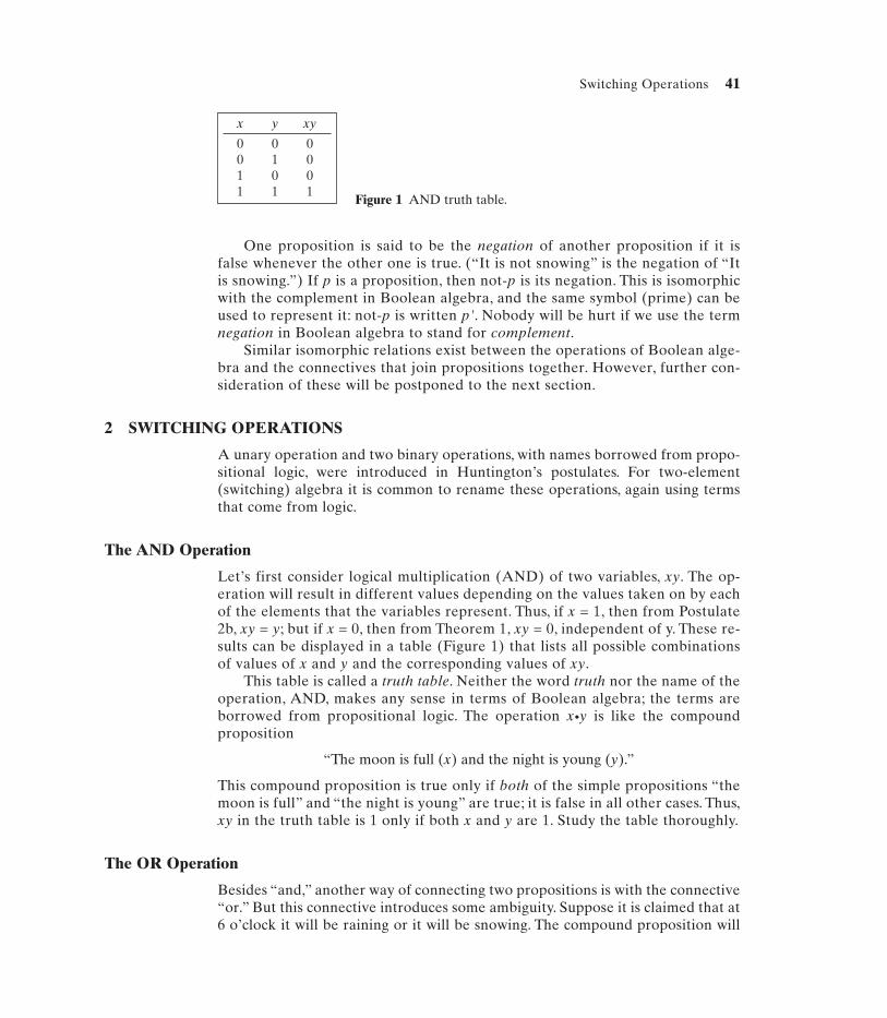
The AND Operation
Let’s first consider logical multiplication (AND) of two variables, xy. The op-eration will result in different values depending on the values taken on by eachof the elements that the variables represent. Thus, if x = 1, then from Postulate2b, xy = y; but if x = 0, then from Theorem 1, xy = 0, independent of y. These re-sults can be displayed in a table (Figure 1) that lists all possible combinationsof values of x and y and the corresponding values of xy.
This table is called a truth table. Neither the word truth nor the name of theoperation, AND, makes any sense in terms of Boolean algebra; the terms areborrowed from propositional logic. The operation x•y is like the compoundproposition
“The moon is full (x) and the night is young (y).”
This compound proposition is true only if both of the simple propositions “themoon is full” and “the night is young” are true; it is false in all other cases. Thus,xy in the truth table is 1 only if both x and y are 1. Study the table thoroughly.
The OR Operation
Besides “and,” another way of connecting two propositions is with the connective“or.” But this connective introduces some ambiguity. Suppose it is claimed that at6 o’clock it will be raining or it will be snowing. The compound proposition will
x y xy
0 0 00 1 01 0 01 1 1
Figure 1 AND truth table.
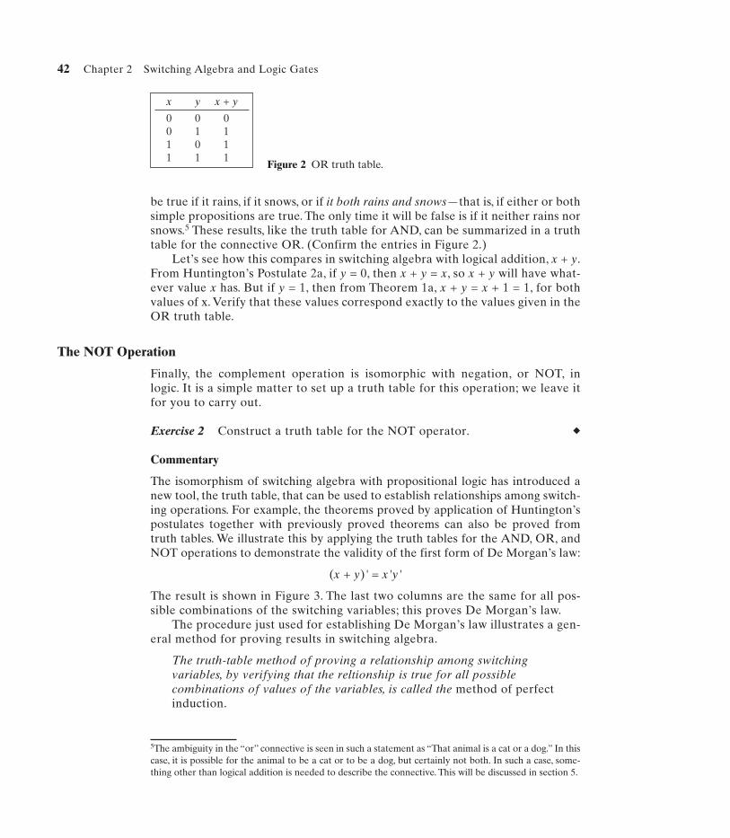
be true if it rains, if it snows, or if it both rains and snows—that is, if either or bothsimple propositions are true. The only time it will be false is if it neither rains norsnows.5 These results, like the truth table for AND, can be summarized in a truthtable for the connective OR. (Confirm the entries in Figure 2.)
Let’s see how this compares in switching algebra with logical addition, x + y.From Huntington’s Postulate 2a, if y = 0, then x + y = x, so x + y will have what-ever value x has. But if y = 1, then from Theorem 1a, x + y = x + 1 = 1, for bothvalues of x. Verify that these values correspond exactly to the values given in theOR truth table.
The NOT Operation
Finally, the complement operation is isomorphic with negation, or NOT, inlogic. It is a simple matter to set up a truth table for this operation; we leave itfor you to carry out.
Exercise 2 Construct a truth table for the NOT operator. �
Commentary
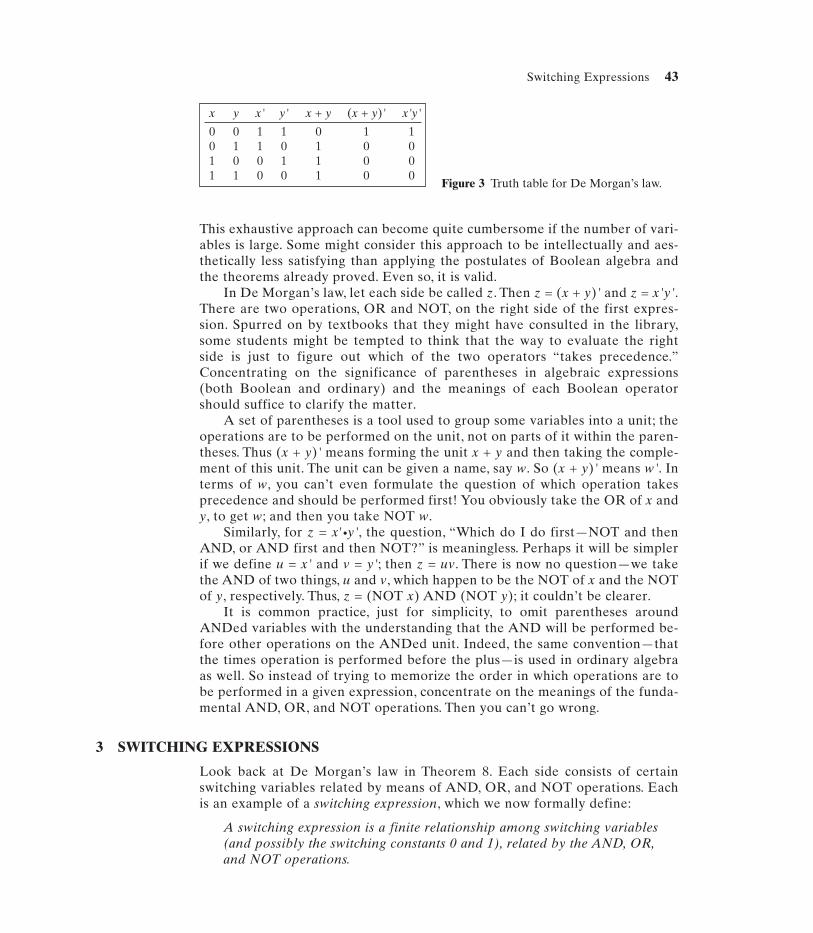
The isomorphism of switching algebra with propositional logic has introduced anew tool, the truth table, that can be used to establish relationships among switch-ing operations. For example, the theorems proved by application of Huntington’spostulates together with previously proved theorems can also be proved fromtruth tables. We illustrate this by applying the truth tables for the AND, OR, andNOT operations to demonstrate the validity of the first form of De Morgan’s law:
(x + y)' = x'y'
The result is shown in Figure 3. The last two columns are the same for all pos-sible combinations of the switching variables; this proves De Morgan’s law.
The procedure just used for establishing De Morgan’s law illustrates a gen-eral method for proving results in switching algebra.
The truth-table method of proving a relationship among switchingvariables, by verifying that the reltionship is true for all possiblecombinations of values of the variables, is called the method of perfectinduction.
42 Chapter 2 Switching Algebra and Logic Gates
5The ambiguity in the “or” connective is seen in such a statement as “That animal is a cat or a dog.” In thiscase, it is possible for the animal to be a cat or to be a dog, but certainly not both. In such a case, some-thing other than logical addition is needed to describe the connective. This will be discussed in section 5.
Figure 2 OR truth table.
x y x + y
0 0 00 1 11 0 11 1 1
This exhaustive approach can become quite cumbersome if the number of vari-ables is large. Some might consider this approach to be intellectually and aes-thetically less satisfying than applying the postulates of Boolean algebra andthe theorems already proved. Even so, it is valid.
In De Morgan’s law, let each side be called z. Then z = (x + y)' and z = x'y'.There are two operations, OR and NOT, on the right side of the first expres-sion. Spurred on by textbooks that they might have consulted in the library,some students might be tempted to think that the way to evaluate the rightside is just to figure out which of the two operators “takes precedence.”Concentrating on the significance of parentheses in algebraic expressions(both Boolean and ordinary) and the meanings of each Boolean operatorshould suffice to clarify the matter.
A set of parentheses is a tool used to group some variables into a unit; theoperations are to be performed on the unit, not on parts of it within the paren-theses. Thus (x + y)' means forming the unit x + y and then taking the comple-ment of this unit. The unit can be given a name, say w. So (x + y)' means w'. Interms of w, you can’t even formulate the question of which operation takesprecedence and should be performed first! You obviously take the OR of x andy, to get w; and then you take NOT w.
Similarly, for z = x'•y', the question, “Which do I do first—NOT and thenAND, or AND first and then NOT?” is meaningless. Perhaps it will be simplerif we define u = x' and v = y'; then z = uv. There is now no question—we takethe AND of two things, u and v, which happen to be the NOT of x and the NOTof y, respectively. Thus, z = (NOT x) AND (NOT y); it couldn’t be clearer.
It is common practice, just for simplicity, to omit parentheses aroundANDed variables with the understanding that the AND will be performed be-fore other operations on the ANDed unit. Indeed, the same convention—thatthe times operation is performed before the plus—is used in ordinary algebraas well. So instead of trying to memorize the order in which operations are tobe performed in a given expression, concentrate on the meanings of the funda-mental AND, OR, and NOT operations. Then you can’t go wrong.
3 SWITCHING EXPRESSIONS
Look back at De Morgan’s law in Theorem 8. Each side consists of certainswitching variables related by means of AND, OR, and NOT operations. Eachis an example of a switching expression, which we now formally define:
A switching expression is a finite relationship among switching variables(and possibly the switching constants 0 and 1), related by the AND, OR,and NOT operations.
Switching Expressions 43
Figure 3 Truth table for De Morgan’s law.
x y x' y' x + y (x + y)' x'y'
0 0 1 1 0 1 10 1 1 0 1 0 01 0 0 1 1 0 01 1 0 0 1 0 0
Some simple examples of switching expressions are xx' + x, z(x + y')',and y + 1.A more complex example of a switching expression is
E = (x + yz)(x + y') + (x + y)'
where E stands for “expression.”Note that expressions are made up of variables, or their complements, on which
various operations are to be performed. For simplicity, we refer to variables or com-plements of variables as literals. The expression E consists of the logical product oftwo expressions logically added to another term. (When discussing logical sums andproducts, we will usually drop the adjective logical for simplicity. But remember thatit is always implied.) The second term in the product is itself a sum of literals, x + y'.The first term in the product cannot be described simply as a sum or a product.
A given expression can be put in many equivalent forms by applying Booleanlaws (that’s what we will call the postulates and theorems for short). But, you mightask, what’s the point? Why bother to perform a lot of algebra to get a differentform? At this time we’ll give only a tentative, incomplete answer. Each switchingvariable in an expression presumably represents a signal; the logical operations areto be implemented (carried out) by means of units of hardware whose overall out-put is to correspond to the expression in question. If a given expression can be rep-resented in different forms, then different combinations of hardware can be usedto give the same overall result. Presumably, some configurations of hardware haveadvantages over others. More systematic methods for treating different represen-tations of switching expressions will be taken up in Chapter 3; their implementa-tion will be continued in Chapter 4. Here we are only setting the stage.
We return now to expression E, renamed E1 in what follows. Equivalent ex-pressions can be found by applying specific laws of switching algebra. Applyingthe distributive law to the product term and De Morgan’s law to the last termleads to E2; then
E1 = (x + yz)(x + y') + (x + y)'E2 = xx + xy' + xyz + y'yz + x'y'E3 = x + x (y' + yz) + x'y' Theorem 3a, Postulates 4a and 5bE4 = x + x'y' Postulate 4a and Theorem 4aE5 = x + y' Theorem 5a
A fairly complicated expression has been reduced to a rather simple one. Note thatE2 contains a term yy', which equals the identity element 0. We say the expressionis redundant. More generally, an expression will be redundant if it contains
• Repeated literals (xx or x + x)• A variable and its complement (xx' or x + x')• Explicitly shown switching constants (0 or 1)
Redundancies in expressions need never be implemented in hardware; they canbe eliminated from expressions in which they show up.
Minterms, Maxterms, and Canonic Forms
Given an expression dependent on n variables, there are two specific andunique forms into which the expression can always be converted. These formsare the subject of this section.
44 Chapter 2 Switching Algebra and Logic Gates
Switching Expressions 45
The expression E1 in the preceding section had mixtures of terms that wereproducts or sums of other terms. Furthermore, although E1 seemed to be dependenton three variables, one of these variables was redundant. The final, equivalent formwas the sum of two terms, each being a single literal.
In the general case, expressions are dependent on n variables.We will consider twononredundant cases. In one case, an expression consists of nothing but a sum of terms,and each term is made up of a product of literals. Naturally, this would be called a sum-of-products (s-of-p) form.The maximum number of literals in a nonredundant productis n. In the second case to be considered, an expression consists of nothing but a prod-uct of terms, and each term is made up of a sum of literals; this is the product-of-sums(p-of-s) form. Again, the maximum number of literals in a nonredundant sum is n.
Suppose that a product term in a sum-of-products expression, or a sum term in aproduct-of-sums form, has fewer than the maximum number n of literals.To distinguishsuch cases from one in which each term is “full,” we make the following definition:
A sum-of-products or product-of-sums expression dependent on n variablesis canonic if it contains no redundant literals and each product or sum hasexactly n literals.6
Each product or sum term in a canonic expression has as many literals as thenumber of variables.
EXAMPLE 1
An example of an expression having three variables, in product-of-sums form, is E1below (not the previous E1). It is converted to sum-of-products form as follows, witheach step justified by the listed switching laws.
E1 = (x' + y' + z)(x + y + z')(x + y + z)E2 = (x' + y' + z)[(x + y)(x + y) + (x + y)(z + z') + zz'] Postulate 4aE3 = (x' + y' + z)(x + y) Postulate 1 and Theorem3bE4 = xy' + x'y + xz + yz Posulates 4a and 5b,Theorem 7
In going from E1 to E4, redundancies were eliminated at each step. The originalexpression is in product-of-sums form, with the maximum number of literals ineach term; hence, it is canonic. The final form, on the other hand, is in sum-of-products form, but it is not canonic; it has only two literals in each term.
Given a noncanonic sum-of-products expression, it is always possible to convertit to canonic form—if there is some reason to do so! The term xy' in expression E4,for example, has the variable z missing. Hence, multiply the term by z + z', whichequals 1 and so does not change the logical value; then expand.The same idea can beused with the other terms. Carrying out these steps on E4 leads to the following:
E5 = xy'(z + z') + x'y(z + z') + xz(y + y') + yz(x + x')
E6 = xy'z + xy'z' + x'yz + x'yz' + xyz
6Some authors use canonical instead of canonic.
46 Chapter 2 Switching Algebra and Logic Gates
(You should confirm the last line; note that redundancies that are created in thefirst line by applying Postulate 4a have to be removed.) This is now in canonicsum-of-products form. �
In a sum-of-products expression dependent on n variables, in order to dis-tinguish between product terms having n literals (the maximum) and those hav-ing fewer than n, the following definition is made:
A canonic nonredundant product of literals is called a minterm.7
That is, a minterm is a nonredundant product of as many literals as there arevariables in a given expression. Thus, each term in E6 is a minterm, and so theentire expression is a sum of minterms.
The same idea applies to a product-of-sums expression. To distinguish be-tween product terms having the maximum number of literals and others, thefollowing definition is made:
A canonic nonredundant sum of literals is called a maxterm.
Each factor in expression E1 in the preceding development is a maxterm; the en-tire expression is a product of maxterms. If a product-of-sums expression is notinitially canonic, it is possible to convert it to canonic form in a manner similar tothe one used for the sum-of-products case, but with the operations interchanged.
Exercise 3 Convert the following expression to a canonic product of max-terms: E = (x + y')(y' + z').Answer8
Generalization of De Morgan’s Law
One of the Boolean laws that has found wide application is De Morgan’s law.It was first stated as Theorem 8 in terms of two variables. It and its dual form,where the sum and product operations are interchanged, are repeated here:
(a) (x1 + x2)' = x1'x2' and (b) (x1x2)' = x1' + x2'
In words, complementing the sum (product) of two switching variables gives thesame result as multiplying (adding) their complements. Suppose we were to increasethe number of variables to three; would the result still hold true? That is, we want toperform the following operation: (A + B + C)'. Let’s rename A + B as D; then whatwe want is (D + C)'. But that’s just D'C', by De Morgan’s law for two variables; andagain by De Morgan’s law, D' = (A + B)' = A'B'. Hence, the final result is:
(a) (A + B + C)' = A'B'C' (b) (ABC)' = A' + B' + C' (1)
(The second form follows by duality.)
7The name doesn’t seem to make sense—what is “min” about it? If anything, from the fact that we hadto go from terms with two literals to ones with three literals, one would think it should be called “max”!Your annoyance will have to persist until Chapter 3, when the whole thing will be clarified.8E = (x + y' + z)(x + y' + z')(x' + y' + z') �
Why stop with three variables? The general case can be written as follows:
(x1 + x2 + ... + xn)' = x1'x2' ... xn' (2)
(x1x2x3... xn)' = x1' + x2' + ... + xn' (3)
In words, (2) says that the complement of the logical sum of any number ofswitching variables equals the logical product of the complements of thosevariables. (In different terms, the NOT of a string of ORs is the AND of theNOTs of the variables in that string.) In (3), we interchange the operationsAND and OR. Just writing the generalization doesn’t make it true; it is left foryou to prove.
Exercise 4 Prove one of the generalized De Morgan laws by mathematical in-duction. That is, assume it is true for k variables, and show that it is true for k + 1.Since we know it is true for two variables, then it will be true for three, (as alreadyproved); since it is true for three, then ... and so on. �
Something more general can be concluded from De Morgan’s law. In (2)and (3), the generalization involves increasing the number of variables in thetheorem. On the left sides, the operations whose NOT is being taken are thesum and product. Suppose now that it is these operations that are generalized!That is, on the left, we are to take the complement of some expression that de-pends on n variables, where the + and • operations are performed in variouscombinations. Will the result be the same if we take the same expression but in-terchange the sum and product operations while complementing all the vari-ables? The generalization is
E'(x1, x2, ... , xn, +, •) = E( x1', x2', ... , xn', •, +) (4)
Note the order of the sum and product operations on each side; it indicates thatthe two operations are interchanged on the two sides, wherever they appear. Theresult can be proved (we won’t do it here) by mathematical induction on the num-ber of operations. (You can do it, if you want.)
EXAMPLE 2
The following expression is given: E = xy'z + x'y'z' + x'yz. To find the comple-ment of E, we interchange the + and • operations and replace each variable byits complement. Thus,
E' = (x' + y + z')•(x + y + z)•(x + y' + z')
Let us first rewrite this expression in sum-of-products form by carrying out theproduct operations on the terms within parentheses and using necessary Boolean al-gebra to simplify. (You carry out the steps before you check your work in what follows.)
E' = (x'y + x'z + yx + y + yz + z'x + z'y)(x + y' + z')
= (x'z + xz' + y)(x + y' + z')
= xy + yz' + x'y'z + xz'
Switching Expressions 47
To verify that this expression correctly gives the complement of E, you cantake its complement using the same generalization of De Morgan’s law and seeif the original expression for E results. �
Exercise 5 Take the complement of E' in the preceding expression, using (4).Put the result in sum-of-products form and verify that the result is the same Eas given in Example 2. �
4 SWITCHING FUNCTIONS
In the preceding section we saw several examples in which a given switching ex-pression was converted to other, equivalent expressions by applying Booleanlaws to it. The equivalent expressions have the same logic values for all combi-nations of the variable values. The concept of “function” plays a very importantrole in ordinary algebra. So far, such a concept has not been introduced forswitching algebra. We will do so now.
The discussion will start by considering two simple expressions:
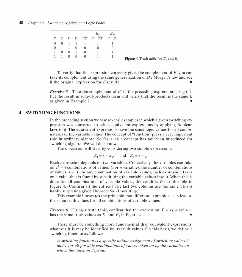
E1 = x + x'y' and E2 = x + y'
Each expression depends on two variables. Collectively, the variables can takeon 22 = 4 combinations of values. (For n variables, the number of combinationsof values is 2n.) For any combination of variable values, each expression takeson a value that is found by substituting the variable values into it. When this isdone for all combinations of variable values, the result is the truth table inFigure 4. (Confirm all the entries.) The last two columns are the same. This ishardly surprising given Theorem 5a. (Look it up.)
This example illustrates the principle that different expressions can lead tothe same truth values for all combinations of variable values.
Exercise 6 Using a truth table, confirm that the expression: E = xy + xy' + y'has the same truth values as E1 and E2 in Figure 4. �
There must be something more fundamental than equivalent expressions;whatever it is may be identified by its truth values. On this basis, we define aswitching function as follows:
A switching function is a specific unique assignment of switching values 0and 1 for all possible combinations of values taken on by the variables onwhich the function depends.
48 Chapter 2 Switching Algebra and Logic Gates
Figure 4 Truth table for E1 and E2
E1: E2:x y x' y' x'y' x + x'y' x + y'
0 0 1 1 1 1 10 1 1 0 0 0 01 0 0 1 0 1 11 1 0 0 0 1 1
For a function of n variables there are 2n possible combinations of values.For each combination of values, the function can take on one of two values.Hence, the number of distinct assignments of two values to 2n things is 2 to the2n power. Hence,
The number of switching functions of n variables is 2 to the 2n.
On this basis, there are 16 switching functions of two variables and 256 func-tions of three variables; the number escalates rapidly for more variables.
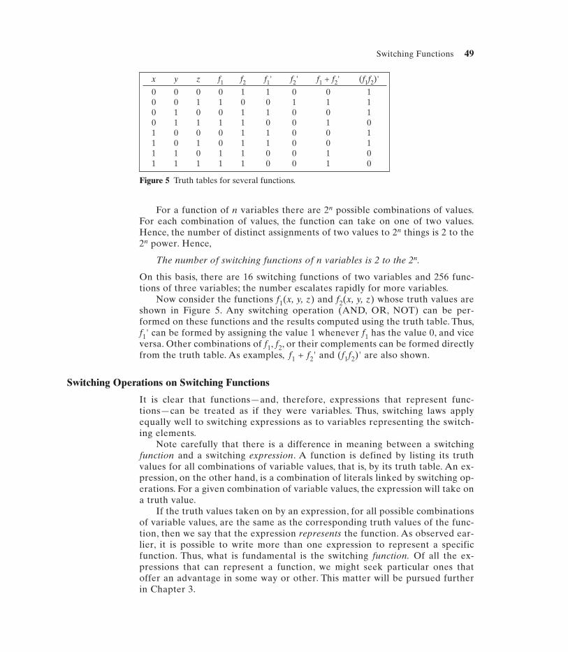
Now consider the functions f1(x, y, z) and f2(x, y, z) whose truth values areshown in Figure 5. Any switching operation (AND, OR, NOT) can be per-formed on these functions and the results computed using the truth table. Thus,f1' can be formed by assigning the value 1 whenever f1 has the value 0, and viceversa. Other combinations of f1, f2, or their complements can be formed directlyfrom the truth table. As examples, f1 + f2' and (f1f2)' are also shown.
Switching Operations on Switching Functions
It is clear that functions—and, therefore, expressions that represent func-tions—can be treated as if they were variables. Thus, switching laws applyequally well to switching expressions as to variables representing the switch-ing elements.
Note carefully that there is a difference in meaning between a switchingfunction and a switching expression. A function is defined by listing its truthvalues for all combinations of variable values, that is, by its truth table. An ex-pression, on the other hand, is a combination of literals linked by switching op-erations. For a given combination of variable values, the expression will take ona truth value.
If the truth values taken on by an expression, for all possible combinationsof variable values, are the same as the corresponding truth values of the func-tion, then we say that the expression represents the function. As observed ear-lier, it is possible to write more than one expression to represent a specificfunction. Thus, what is fundamental is the switching function. Of all the ex-pressions that can represent a function, we might seek particular ones thatoffer an advantage in some way or other. This matter will be pursued furtherin Chapter 3.
Switching Functions 49
Figure 5 Truth tables for several functions.
x y z f1 f2 f1' f2' f1 + f2' (f1f2)'
0 0 0 0 1 1 0 0 10 0 1 1 0 0 1 1 10 1 0 0 1 1 0 0 10 1 1 1 1 0 0 1 01 0 0 0 1 1 0 0 11 0 1 0 1 1 0 0 11 1 0 1 1 0 0 1 01 1 1 1 1 0 0 1 0
50 Chapter 2 Switching Algebra and Logic Gates
Number of Terms in Canonic Forms
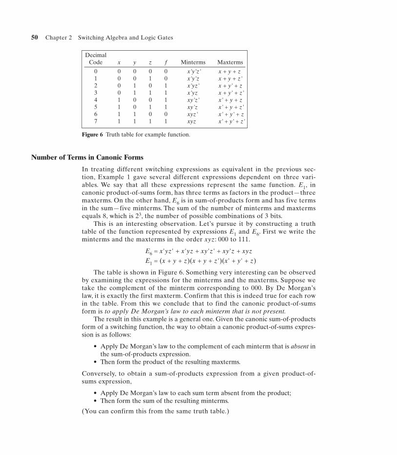
In treating different switching expressions as equivalent in the previous sec-tion, Example 1 gave several different expressions dependent on three vari-ables. We say that all these expressions represent the same function. E1, incanonic product-of-sums form, has three terms as factors in the product—threemaxterms. On the other hand, E6 is in sum-of-products form and has five termsin the sum—five minterms. The sum of the number of minterms and maxtermsequals 8, which is 23, the number of possible combinations of 3 bits.
This is an interesting observation. Let’s pursue it by constructing a truthtable of the function represented by expressions E1 and E6. First we write theminterms and the maxterms in the order xyz: 000 to 111.
E6 = x'yz' + x'yz + xy'z' + xy'z + xyz
E1 = (x + y + z)(x + y + z')(x' + y' + z)
The table is shown in Figure 6. Something very interesting can be observedby examining the expressions for the minterms and the maxterms. Suppose wetake the complement of the minterm corresponding to 000. By De Morgan’slaw, it is exactly the first maxterm. Confirm that this is indeed true for each rowin the table. From this we conclude that to find the canonic product-of-sumsform is to apply De Morgan’s law to each minterm that is not present.
The result in this example is a general one. Given the canonic sum-of-productsform of a switching function, the way to obtain a canonic product-of-sums expres-sion is as follows:
• Apply De Morgan’s law to the complement of each minterm that is absent inthe sum-of-products expression.
• Then form the product of the resulting maxterms.
Conversely, to obtain a sum-of-products expression from a given product-of-sums expression,
• Apply De Morgan’s law to each sum term absent from the product;• Then form the sum of the resulting minterms.
(You can confirm this from the same truth table.)
Figure 6 Truth table for example function.
DecimalCode x y z f Minterms Maxterms
0 0 0 0 0 x'y'z' x + y + z1 0 0 1 0 x'y'z x + y + z'2 0 1 0 1 x'yz' x + y' + z3 0 1 1 1 x'yz x + y' + z'4 1 0 0 1 xy'z' x' + y + z5 1 0 1 1 xy'z x' + y + z'6 1 1 0 0 xyz' x' + y' + z7 1 1 1 1 xyz x' + y' + z'
Switching Functions 51
Exercise 7 Given the product-of-sums expression in E1 in this section, use thepreceding approach to find the corresponding sum-of-products form. �
This approach avoids the necessity of carrying out switching algebra toconvert from one form to another; instead, given one of the two forms, you canfind the other one by mentally carrying out some steps merely by inspection.
Shannon’s Expansion Theorem
Previous examples have shown that more than one expression can representthe same switching function. Two specific expressions noted are the sum-of-products and product-of-sums forms. The question arises as to whether a givenfunction can always be expressed in these specific standard forms. An answer tothis question, which is the subject of this section, was provided by ClaudeShannon.9
Sum-of-Products Form
Suppose that f(x1, x2, ..., xn) is any switching function of n variables. Shannonshowed that one way of expressing this function is
f(x1, x2, ..., xn) = x1f(1, x2, ..., xn) + x1'f(0, x2, ..., xn) (5)
On the right side, the function is the sum of two terms, one of them relevantwhen x1 takes on the value 1 and the other when x1 takes on the value 0. Thefirst term is x1 times what remains of f when x1 takes on the value 1; the secondterm is x1' times what remains of f when x1 takes on the value 0. The proof ofthis expression is easy; it follows by perfect induction. That is, if the result istrue for all possible values of variable x1 (there are only two values—1 and 0)it must be true, period. (Confirm that it is true for both values of x1.)
You can surely see how to proceed: Repeat the process on each of the re-maining functions, this time using another variable, say x2. Continue theprocess until all variables are exhausted. The result is simply a sum of terms,each of which consists of the product of n literals multiplied by whatever thefunction becomes when each variable is replaced by either 0 or 1. But the lat-ter is simply the value of the function when the variables collectively take onsome specific combination of values; this value is either 0 or 1. So the end re-sult is a sum of all possible nonredundant products of the 2n literals (the nvariables and their complements), some of which are multiplied by 1 and theremaining ones by 0. The latter are simply absent in the final result. Accordingto Shannon, this will equal the original function. The proof at each step is byperfect induction.
Shannon’s expansion theorem in the general case is
f = a0 x1'x2' ... xn' + a1x1'x2' ... xn–1'xn + a2x1'x2' ... xn–1xn' + ...+ a2n–2 x1x2
... xn' + a2n–1 x1x2... xn (6)
9Claude E. Shannon,“A Symbolic Analysis of Relay and Switching Circuits,” Trans AIEE, 57 (1938), 713–723.
52 Chapter 2 Switching Algebra and Logic Gates
Each ai is a constant in which the subscript is the decimal equivalent of the mul-tiplier of ai viewed as a binary number. Thus, for three variables, a5 (binary 101)is the coefficient of x1x2'x3.
Shannon’s expansion theorem in (6) is a major result. It shows that
Any switching function of n variables can be expressed as a sum ofproducts of n literals, one for each variable.
Exercise 8 Let f be a function of two variables, x1 and x2. Suppose that f takeson the value 1 for the combinations x1x2: 00, 10, 11 and the value 0 for the re-maining combination. Determine the expression resulting from Shannon’s ex-pansion theorem carried out to completion in this case. As an added task, notdependent on Shannon’s theorem, simplify the result if possible.Answer10
In carrying the expansion process in (6) through to completion, a subcon-scious assumption has been made. That assumption is that, at each step until thelast, after some (but not all) variables have been replaced by constants, the func-tion that remains is itself not a constant. That is, what remains still depends on theremaining variables. If, instead, this remaining function reduces to a constant, theprocess will prematurely terminate and the corresponding term will have fewerthan n literals. We have already discussed in the preceding section how to restoreany missing literals. Hence, even in such a case, the generalization is valid.
Shannon’s theorem constitutes an “existence proof.” That is, it proves by aspecific procedure that a certain result is true. Once the proof is established,then for any particular example it isn’t necessary to follow the exact procedureused to prove the theorem. Now that we know that a function can always be putinto the stated form, we can search for easier ways of doing it.
Product-of-Sums Form
Shannon’s expansion theorem in (6) is a sum-of-products form. It’s easy to sur-mise that a similar result holds for the product-of-sums form. It isn’t necessaryto go through an extensive proof for this form. The result can be obtained from(5) and (6) by duality. That is, 0 and 1 are interchanged, as are the sum andproduct operations. Doing this, the counterparts of (5) and (6) become
f(x1, x2, ... , xn) = [x1 + f(0, x2, ... , xn)][x1' + f(1, x2, ... , xn)] (7)
f = (b0 + x1' + x2' + ... + xn')(b1 + x1' + ... +xn–1' + xn) ...(bn–2 + x1 + x2 + ... + xn')(bn–1 + x1 + x2 + ... + xn) ... (8)
where the bi are the constants 0, 1. These equations are the duals of (5) and (6).The last one shows that
Any switching function of n variables can be expressed as a product ofsums of n literals, one for each variable.
If the expansion should terminate prematurely, the missing literals can al-ways be restored by the approach illustrated in the last section. The constants
10 f = x1'x2' + x1x2' + x1x2 = x1 + x2' �
will not show up explicitly in an actual function after redundancies are re-moved. If one of the constants is 1, for example, the entire corresponding fac-tor will be 1, since 1 + x = 1, and the corresponding factor will not be present.On the other hand, if any constant is 0, since 0 + x = x, this constant does notshow up but the corresponding factor will be present.
Exercise 9 Use the process of Shannon’s theorem step by step to put the func-tion in Exercise 8 in a product-of-sums form. Simplify the result, if possible. �
5 OTHER SWITCHING OPERATIONS
It was noted earlier that propositional logic is isomorphic with switching alge-bra. As already observed, the language of propositional logic has permeated theway in which operations and ideas are discussed in switching algebra. We willnow borrow some other operations that arise naturally in propositional logicand convert them to our use.
Exclusive OR
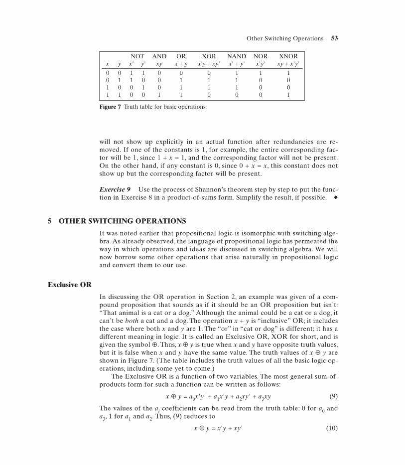
In discussing the OR operation in Section 2, an example was given of a com-pound proposition that sounds as if it should be an OR proposition but isn’t:“That animal is a cat or a dog.” Although the animal could be a cat or a dog, itcan’t be both a cat and a dog. The operation x + y is “inclusive” OR; it includesthe case where both x and y are 1. The “or” in “cat or dog” is different; it has adifferent meaning in logic. It is called an Exclusive OR, XOR for short, and isgiven the symbol ⊕. Thus, x ⊕ y is true when x and y have opposite truth values,but it is false when x and y have the same value. The truth values of x ⊕ y areshown in Figure 7. (The table includes the truth values of all the basic logic op-erations, including some yet to come.)
The Exclusive OR is a function of two variables. The most general sum-of-products form for such a function can be written as follows:
x ⊕ y = a0x'y' + a1x'y + a2xy' + a3xy (9)
The values of the ai coefficients can be read from the truth table: 0 for a0 anda3, 1 for a1 and a2. Thus, (9) reduces to
x ⊕ y = x'y + xy' (10)
Other Switching Operations 53
Figure 7 Truth table for basic operations.
NOT AND OR XOR NAND NOR XNORx y x' y' xy x + y x'y + xy' x' + y' x'y' xy + x'y'
0 0 1 1 0 0 0 1 1 10 1 1 0 0 1 1 1 0 01 0 0 1 0 1 1 1 0 01 1 0 0 1 1 0 0 0 1
Exercise 10 Starting with the sum-of-products form for the XOR in (10), ob-tain a canonic product-of-sums form.Answer11
NAND, NOR, and XNOR Operations
Besides the NOT operation, we now have three in our repertoire: AND, OR,and XOR. Three additional operations can be created by negating (comple-menting, or taking the NOT of) these three:
NAND (NOT AND): (xy)' = x' + y' (11)
NOR (NOT OR): (x + y)' = x'y' (12)
XNOR (NOT XOR): (x ⊕ y)' = (x'y + xy')' = xy + x'y' (13)
The right side in (13) can be obtained from (10) by negating the truth values ofXOR to obtain the values of ai. (Confirm it.) The truth values for these threeare easily obtained from the three operations of which they are the NOTs. Allthe results are shown in the preceding truth table (Figure 7).
Exercise 11 Discuss the nature of the right sides of (11) and (12) as sum-of-products or product-of-sums forms. �
Exercise 12 Apply switching laws to find a product-of-sums form of the right sideof (13). �
Notice from Figure 7 that XNOR is 1 whenever x and y have the same value. Inlogic, the function of two variables that equals 1 whenever the two variables have thesame value is called an equivalence relation. The symbol denoting an equivalence re-lation is a two-headed arrow, x ⇔ y. Thus, XNOR and equivalence have the sametruth values and can be used interchangeably: A XNOR B = A ⇔ B = xy + x'y'.
Comparing two signals (inputs) to see if they are the same is an importantoperation in many digital systems. Thus, an XNOR gate is a one-bit comparator;when its output is 1, we know that the two inputs are the same. We will discusshow to use XNOR gates to compare numbers of more than 1 bit in Chapter 3.
Some of you may have some uneasiness with the introduction of XOR andthe other operations in this section. Earlier, a switching expression was definedas one that includes the operators AND, OR, and NOT. Would this mean thatsomething including XOR or the other operations discussed in this section can-not be a switching expression? This apparent contradiction is overcome by not-ing equations (10) to (13). Each of the operations defined by these operators isexpressed in terms of AND, OR, and NOT, so the uneasiness should disappear.
6 UNIVERSAL SETS OF OPERATIONS
Switching algebra was introduced in terms of two binary operations (AND andOR) and one unary operation (NOT). Every switching expression is made up
54 Chapter 2 Switching Algebra and Logic Gates
11Add xx' and yy', and then use the distributive law: (x + y)(x' + y'). �
Universal Sets of Operations 55
of variables connected by various combinations of these three operators. Thisobservation leads to the following concept:
A set of operations is called universal if every switching function can beexpressed exclusively in terms of operations from this set.
(Some use the term functionally complete in place of universal.) It follows thatthe set of operations {AND, OR, NOT} is universal.
In the preceding section various other operations were introduced. Two ofthese are NAND and NOR:
x NAND y: (xy)' = x' + y' (14)
x NOR y: (x + y)' = x'y' (15)
We see that the right sides of these expressions are each expressed in terms of onlytwo of the three universal operations (OR and NOT for the first, and AND andNOT for the second). This prompts a general question: Can one of the three oper-ations be removed from the universal set and still leave a universal set? The answeris “yes, indeed” if one of the operations can be expressed in terms of the other two.
Consider the AND operation, xy. By De Morgan’s law, it can be written as
xy = (x' + y')' (16)
The only operations on the right are OR and NOT. Since every AND can be ex-pressed in terms of OR and NOT, the set {AND, OR, NOT} can be expressed interms of the set {OR, NOT}. Conclusion: The set {OR, NOT} is a universal set.
Exercise 13 By reasoning similar to that just used, show that the set {AND,NOT} is a universal set. �
The conclusion just reached is that any switching function can be expressedin terms of only two switching operations. But why stop there—why not try forjust one? Let’s explore the NAND operation. Since the set {AND, NOT} is uni-versal, if we can express both those operations in terms of NAND, then,{NAND} will be universal! Here we go:
x' = x' + x' = (xx)' Theorems 3a and 8a (17)
xy = ((xy)')' = [(xy)' (xy)']' Theorems 2 and 3b (18)
The right sides are expressed in terms of nothing but NAND. Conclusion:
Any switching function can be expressed exclusively in terms of NANDoperations.
Exercise 14 Show by a procedure similar to the one just used that {NOR} is auniversal set. �
The conclusion that results from the preceding exercise is
Any switching function can be expressed exclusively in terms of NOR operations.
The practical point of the preceding discussion is that, in the real world,switching operations are carried out by means of physical devices. If all switching
functions can be expressed in terms of just one operation, then the physical im-plementation of any switching function can be carried out with only one type ofphysical device. This has obvious implications for simplicity, convenience, andcost, which we shall amplify in Chapter 3.
7 LOGIC GATES
Up to this point we have been dealing with rather abstract matters. We havediscussed logic operations in an algebra called switching algebra. The variablesthat are manipulated in switching algebra are abstract switching variables.Nothing has been said so far that relates these switching variables to anythingin the real world. Also, no connection has been made between the operations ofswitching algebra and physical devices.
We are now ready to change all that. For switching algebra to carry out realtasks, physical devices must exist that can carry out the operations of switchingalgebra as accurately and with as little delay as possible. The switching vari-ables, which take on logic values of 0 and 1, must be identified with real signalscharacterized by a physical variable, such as voltage.
The generic name given to a physical device that carries out any of theswitching operations is gate. However, in anticipation of discussing such devices,we will introduce another abstract representation of switching operations, aschematic representation for the real-life devices and for their interconnectionin actual switching circuits.
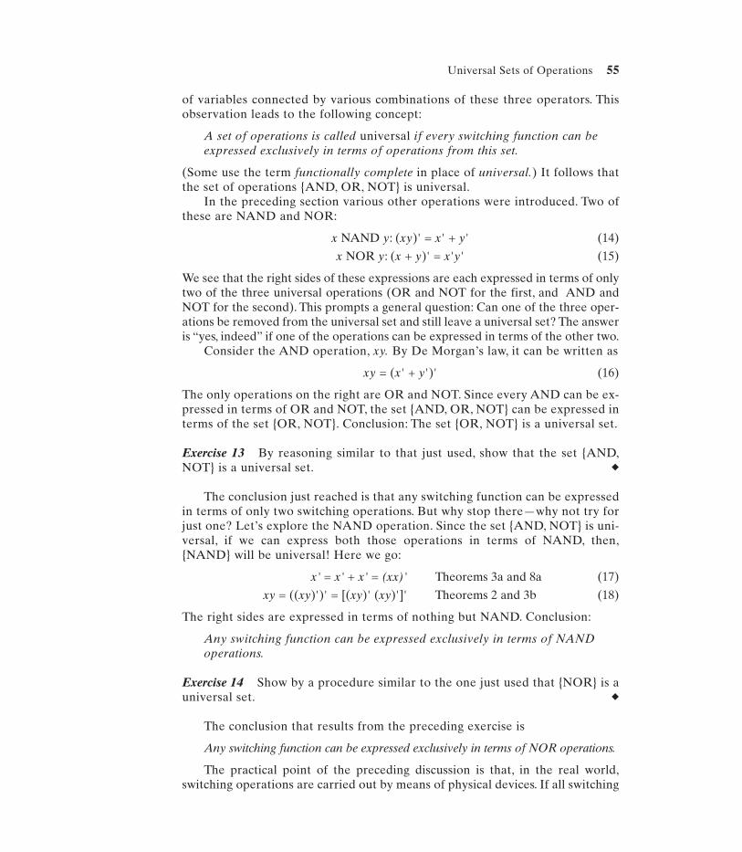
Suppose that each operation in switching algebra is represented by a dif-ferent schematic symbol, with a distinct terminal for each logic variable. Thenany switching expression can be represented by some interconnection of thesesymbols. Attempts have been made in the past to adopt a set of standard sym-bols. One set has a uniform shape for all operations (a rectangle), with the op-eration identified inside.12 A more common set of symbols for gates uses adistinct shape for each operation, as shown in Figure 8.
The NOT gate is called an inverter; each of the others is called by the nameof the operation it performs—an AND gate, a NOR gate, and so on. Althougheach gate (except the inverter) is shown with two input terminals, there may be
56 Chapter 2 Switching Algebra and Logic Gates
12The Institute of Electrical and Electronic Engineers has published such standards (see IEEE Standard91-1984). However, they have not been widely adopted.
Figure 8 Symbols for logic gates.
x x⋅y
ANDy
x (x⋅y)′
x ′
x+y
(x+y)′
x⊕y
NAND
x
NOT
OR
NOR
XOR
y
x
y
x
y
x
y
Logic Gates 57
more than two inputs. (For the real devices of which these gates are abstrac-tions, there are practical limitations on the number of inputs; these limitationswill be discussed shortly.)
There is no problem with having more than two inputs for the two basicBoolean operators AND and OR, because both of these operators satisfy theassociative law. The result is the same if we logically add x to (y + z) or add x +y first and then add it to z; unambiguously, the result is x + y + z. The same istrue of the XOR operation. (Prove this to yourself.) However, the NAND andNOR operations are not associative. The output of a three-input NAND gate is(xyz)'; however, this is not the same as the NAND of x and y followed by theNAND with z. That is, (xyz)' ≠ ((xy)'z)'.
A NAND gate is formed by appending a small circle (called a bubble), rep-resenting an inverter, to the output line of an AND gate. (The same is true forforming a NOR gate from an OR.) Furthermore, placing a bubble on an inputline implies complementing the incoming variable before carrying out the op-eration performed by the gate.
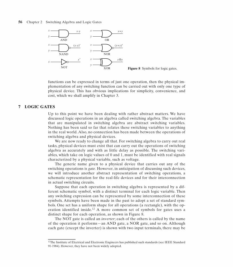
Alternative Forms of NAND and NOR Gates
Other representations of a NAND gate and a NOR gate can be found by an ap-plication of De Morgan’s law. For two variables, De Morgan’s law is
(xy)' = x' + y' (19)
(x + y)' = x'y' (20)
The left sides of (19) and (20) are represented by the NAND and NOR gatesymbols in Figure 8. The right side of (19) is an OR operation on inputs thatare first inverted. Similarly, the right side of (20) is an AND operation on in-verted inputs. These alternative forms of NAND and NOR gates are shown inFigure 9.
As far as ideal logic gates are concerned, the two forms of NAND or NORgates are equally acceptable. However, when it comes to implementing the logicusing real, physical gates, there is a practical difference between the two; weshall discuss this subsequently.
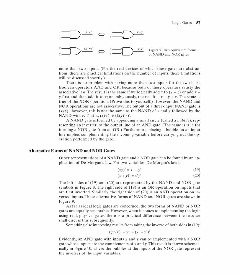
Something else interesting results from taking the inverse of both sides in (19):
((xy)')' = xy = (x' + y')'
Evidently, an AND gate with inputs x and y can be implemented with a NORgate whose inputs are the complements of x and y. This result is shown schemat-ically in Figure 10, where the bubbles at the inputs of the NOR gate representthe inverses of the input variables.
Figure 9 Two equivalent formsof NAND and NOR gates.
x x′⋅y′y
x (xy)′ x′+y′
y
xy
(x+y)′x
y
58 Chapter 2 Switching Algebra and Logic Gates
Exercise 15 By a procedure similar to that used above, find an equivalentform of an OR expression and draw the corresponding equivalent gates. �
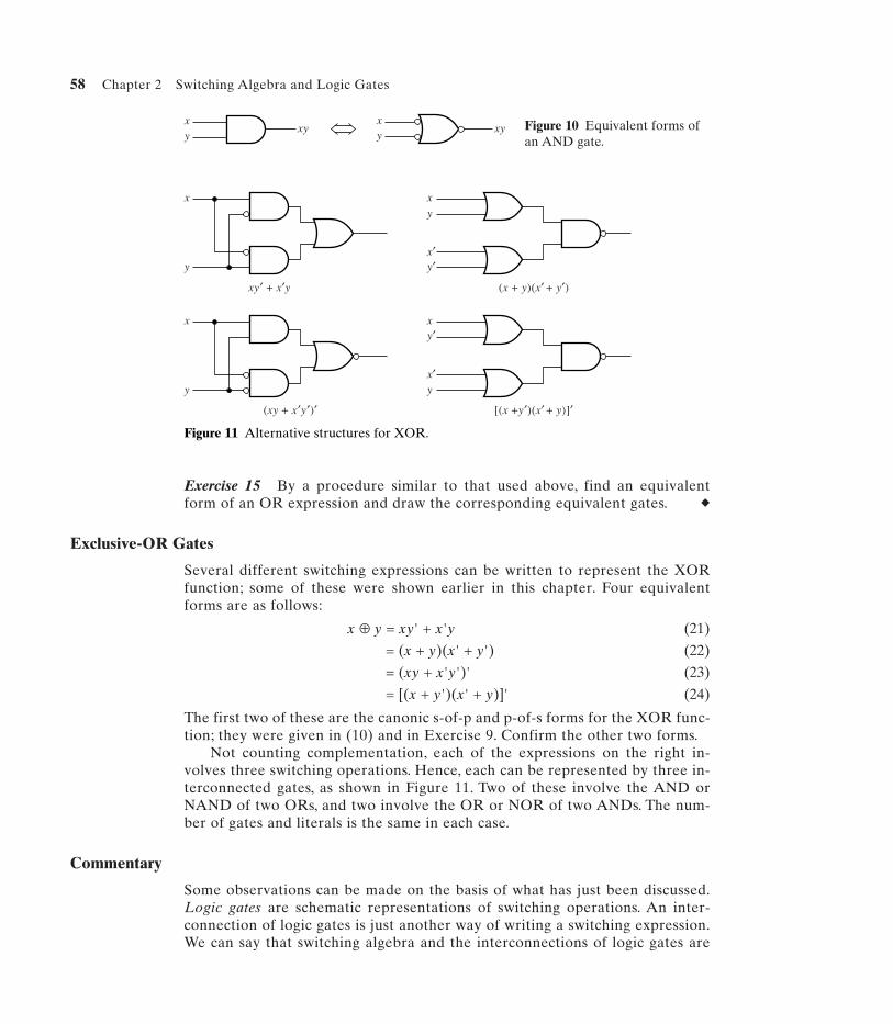
Exclusive-OR Gates
Several different switching expressions can be written to represent the XORfunction; some of these were shown earlier in this chapter. Four equivalentforms are as follows:
x ⊕ y = xy' + x'y (21)
= (x + y)(x' + y') (22)
= (xy + x'y')' (23)
= [(x + y')(x' + y)]' (24)
The first two of these are the canonic s-of-p and p-of-s forms for the XOR func-tion; they were given in (10) and in Exercise 9. Confirm the other two forms.
Not counting complementation, each of the expressions on the right in-volves three switching operations. Hence, each can be represented by three in-terconnected gates, as shown in Figure 11. Two of these involve the AND orNAND of two ORs, and two involve the OR or NOR of two ANDs. The num-ber of gates and literals is the same in each case.
Commentary
Some observations can be made on the basis of what has just been discussed.Logic gates are schematic representations of switching operations. An inter-connection of logic gates is just another way of writing a switching expression.We can say that switching algebra and the interconnections of logic gates are
Figure 10 Equivalent forms ofan AND gate.
xy
xyxyxy
Figure 11 Alternative structures for XOR.
xy′ + x′y
(xy + x′y′)′
x
y
x
y
(x + y)(x′ + y′)
[(x +y′)(x′ + y)]′
x
x′y′
y
x
x′y
y′
Positive, Negative, and Mixed Logic 59
isomorphic systems. When we use schematic symbols called logic gates or drawinterconnections of gates to represent switching operations, there need be noimplication of anything physical or real.
Suppose, however, that physical devices that perform the operations sym-bolized by the gates could be constructed, even if they were not perfect. Thenwe could construct a physical circuit (we might call it a switching circuit) thatcan implement, or realize, a specific switching expression.13 The circuit would bean implementation, or realization, of the expression. This is what makes switch-ing algebra, an abstract mathematical structure, so useful in the physical designof real circuits to carry out desired digital tasks.
As a simple illustration, consider an XOR gate with inputs x and y. Wemight be interested in comparing the inputs. It is clear from (21) that x ⊕ y = 1whenever the values of the two inputs are different. (The opposite would betrue for an XNOR gate.) Thus, either gate can play the role of a comparator of1-bit numbers.
As another illustration, it may not be necessary to explicitly use an inverterto obtain the complement of a switching variable. A certain device that gener-ates a switching variable commonly generates its complement also, so that bothare available.14 Hence, if x and x' both appear in an expression, then in the cor-responding circuit, either we can show separate input lines for both of them orwe can indicate the complement with a bubble. If you glance back at Figure 11,you will see that each of these approaches is used in half the cases.
8 POSITIVE, NEGATIVE, AND MIXED LOGIC
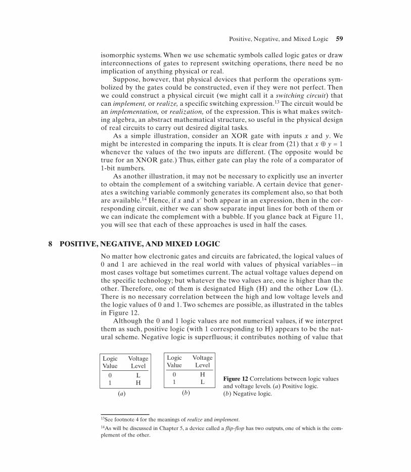
No matter how electronic gates and circuits are fabricated, the logical values of0 and 1 are achieved in the real world with values of physical variables—inmost cases voltage but sometimes current. The actual voltage values depend onthe specific technology; but whatever the two values are, one is higher than theother. Therefore, one of them is designated High (H) and the other Low (L).There is no necessary correlation between the high and low voltage levels andthe logic values of 0 and 1. Two schemes are possible, as illustrated in the tablesin Figure 12.
Although the 0 and 1 logic values are not numerical values, if we interpretthem as such, positive logic (with 1 corresponding to H) appears to be the nat-ural scheme. Negative logic is superfluous; it contributes nothing of value that
13See footnote 4 for the meanings of realize and implement.14As will be discussed in Chapter 5, a device called a flip-flop has two outputs, one of which is the com-plement of the other.
Logic VoltageValue Level
0 L1 H
(a)
Logic VoltageValue Level
0 H1 L
(b)
Figure 12 Correlations between logic valuesand voltage levels. (a) Positive logic.(b) Negative logic.
60 Chapter 2 Switching Algebra and Logic Gates
is not achievable with positive logic. Hence, there is no useful reason for adopt-ing it. However, it may be useful to adopt positive logic at some terminals of de-vices in a circuit and negative logic at other terminals. This possibility isreferred to as mixed logic. Its greatest utility occurs in dealing with real physi-cal circuits. The next few paragraphs will discuss the common terminology inthe use of mixed logic.
Two concepts are utilized in addressing the issues surrounding mixed logic.One is the concept of activity. The normal state of affairs, it might be assumed,as inactivity. The telephone is normally quiet (inactive) until it rings (becomesactive), and conversations can then be carried on. Lights are normally off (in-active) until they are activated by a switch. When a microprocessor is perform-ing a READ operation, it is active. Otherwise it isn’t doing anything; it isinactive.15 Thinking of logic 1 in connection with activity and logic 0 with inac-tivity is just a habit.
At various terminals in a physical system that is designed to carry out dig-ital operations, voltages can have either high (H) or low (L) values. As just dis-cussed, the two ways in which voltage levels and logic values can be associatedare 1 ↔ H and 0 ↔ L, or the opposite, 1 ↔ L and 0 ↔ H. What complicates lifeeven more is that at some points in a circuit the association can be made in oneway and at other points in the opposite way.
Because of the connection of activity with logic 1, if the association of 1 ↔ His made, the scheme is said to be “active high.” If the association 1 ↔ L is made, itis said to be “active low.” But this description employs two steps, two levels of as-sociation: Activity is first connected with logic 1; then logic 1, in turn, is associatedwith a high or a low voltage. Schematically, the train of thought is
activity � logic 1 ↔ high voltage = active high
activity � logic 1 ↔ low voltage = active low
“Active high” means that logic 1 is associated with a high voltage. More simply,one could say 1-high or 1-H instead of “active high.” The adjective active justadds distance to the real association to be established between a logic value anda voltage level.
Another concept sometimes used as a synonym for activity is the notion ofasserting. Thus, “asserted high” and “asserted low” mean the same as “activehigh” and “active low” which, in the end, mean the association of logic 1 with ahigh voltage and with a low voltage, respectively. The reasoning goes somethinglike this: To assert is to affirm, to state that something is so; what is assertedmight be thought to be “true.” In propositional logic, a proposition is either trueor false. So when something is asserted, this is equivalent to saying that theproposition is true. The dichotomy true/false in the logic of propositions is as-sociated with switching constants 1 and 0. But there is no one-to-one corre-spondence between 1-T and 0-F; it is simply customary to associate 1 with“true” and 0 with “false.”
15One might even think of Newton’s first law as exemplifying this contention. Normally, things are in sta-sis; if you want something to change, you have to become active and exert a force.
Some Practical Matters Regarding Gates 61
Anyway, if we associate 1 with “true,” and if assertion means “true,” thenassertion will be associated with 1:
asserted ⇒ true ⇒ logic 1
Hence, saying something is “asserted high” means that 1 corresponds to a highvoltage. The use of “asserted” here adds nothing to the identification of 1 witha high voltage; you might as well say “1-high”, or 1-H. In the same way, sayingthat something is “asserted low” means that 1 corresponds to a low voltage.Here the terminology “asserted” adds nothing to the identification of 1 with alow voltage; you might as well say 1-L.
One final comment on terminology. Sometimes the verb “to assert” is usedin a way that does not connect it to “high” or “low.” It might be said, for ex-ample, that a certain signal must be asserted before something else can hap-pen. In such a usage, there is no commitment to asserting high or assertinglow—just to asserting. This terminology does not require a commitment tomixed logic or positive logic; it can be applied in either case. Hence, it can beuseful terminology.
When physical devices are used to implement a logic diagram, it is possi-ble to use a different correspondence of voltage levels with logic values at dif-ferent input and output terminals—even at internal points. For the actualimplementation phase of a design, it might be useful to consider what is calledmixed logic, in which the correspondence 1-H is made at some device termi-nals and 1-L at others. To achieve this purpose, special conventions and nota-tions are used to convey the information as to which terminals correspond to1-H and which to 1-L.
In this book, we will stick with positive logic, so we will not deal with thisspecial notation. Indeed, the gate symbols shown in Figures 8–11 are based onpositive logic.
9 SOME PRACTICAL MATTERS REGARDING GATES16
Up to this point we have adopted the following viewpoint: The specifications ofa logic task, followed by the procedures of switching algebra, result in a switch-ing expression. A schematic diagram containing logic gates is then constructedto realize this expression. Ultimately, we expect to construct the physical em-bodiment of this diagram using real, physical devices, generically referred to ashardware.
The way in which physical gates are designed and built depends on the tech-nology of the day. As already mentioned, the first switching circuits utilized
16This section is largely descriptive. Although a couple of exercises are slipped in, these do not re-quire a great deal of effort and creativity to complete. What is discussed is highly relevant to labo-ratory work. If you wish, you can be a largely passive reader; but we urge you to become engaged,to take notes, to formulate questions, and to refer to other books and manufacturers’ handbooks forspecific items.
mechanical devices: switches and relays.17 The first switching devices that werecalled “gates” were designed with vacuum tubes. Vacuum tubes were later re-placed by semiconductor diodes and, later still, by bipolar transistors and thenMOSFETs. Each gate was individually constructed with discrete components.
The advent of integrated circuits permitted, first, an entire gate to be fabri-cated as a unit, and then several independent gates. Such small-scale integrated(SSI) units still find use. Soon it became possible to incorporate in the same in-tegrated circuit an interconnection of many gates that together perform certainspecific operations; we will discuss a number of such medium-scale integrated(MSI) circuits in Chapter 4. In time, an entire circuit consisting of hundreds ofthousands of gates—such as a microprocessor—came to be fabricated as a singleunit, on a single “chip.” Some characteristics of integrated circuits will be dis-cussed here. Design using specific circuits of this type will be carried out inChapter 8.
Logic Families
As mentioned briefly above, the design and implementation of logic gates in anygiven era is carried out using the particular devices available at the time. Eachtype of device operates optimally with specific values of power-supply voltage.Different designs can result in different high and low voltage levels. A set of logicgates using a single design technology is referred to as a logic family. Some thatwere considered “advanced” just four decades ago (such as resistor-transistorlogic, or the RTL family) are now obsolete but can still be found in museums.
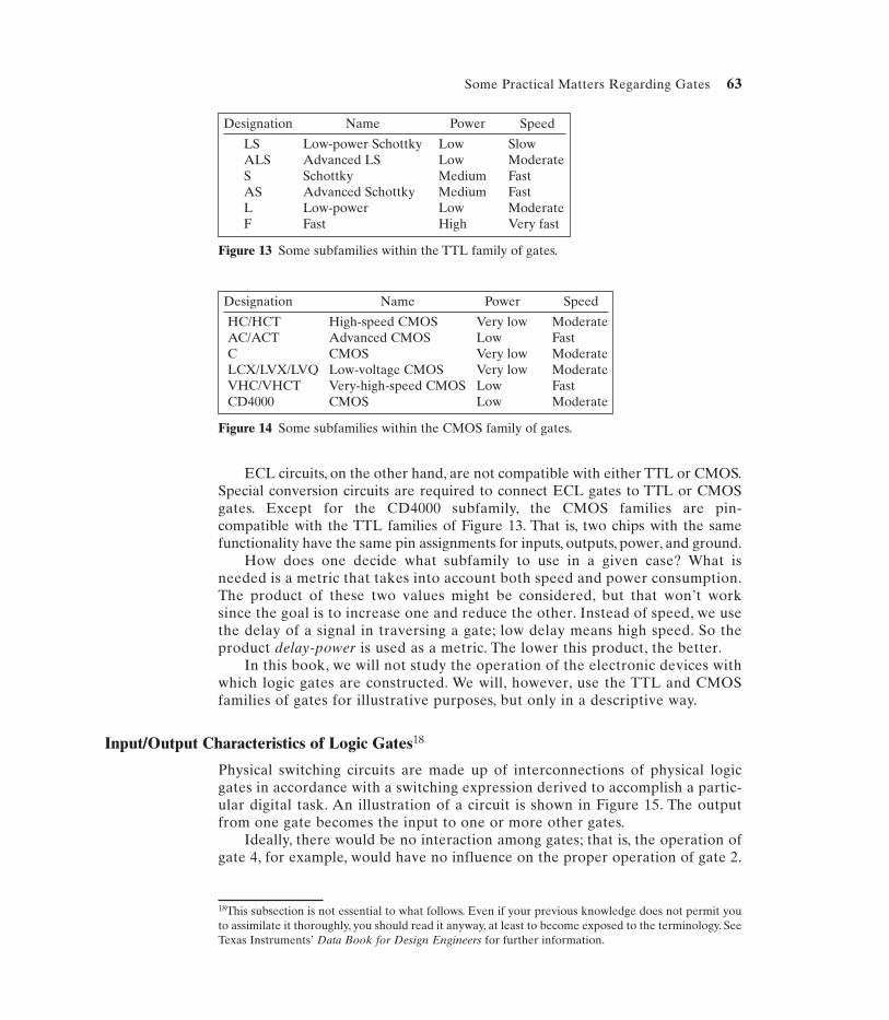
Different designs are developed and promoted by different manufacturers andare suited to different requirements. The ECL (emitter-coupled logic) family cameout of Motorola, while Texas Instruments is the creator of the TTL (transistor-transistor logic) family. The basic TTL design has been modified and improved overtime in different ways to enhance one property of a gate (say speed) at the expenseof some other property (say power consumption). In this way, different subfamiliesare created within the TTL family. A table listing a number of the TTL subfamilies isgiven in Figure 13.
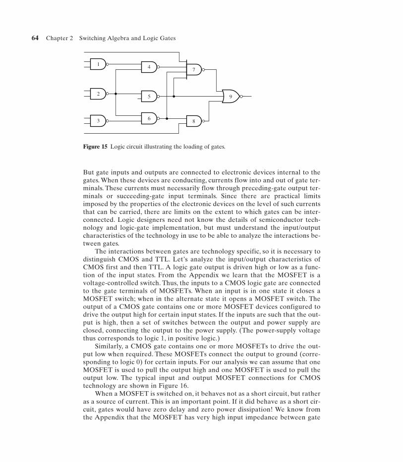
While the TTL and ECL logic families utilize bipolar transistors as the switch-ing element, CMOS (complementary metal-oxide semiconductor) technology uti-lizes the MOSFET transistor. The subfamilies of CMOS are listed in Figure 14. Amajor question arises as to whether the inputs and outputs of CMOS gates can beinterconnected with TTL gates without any special conversion circuits. If they can,we say that CMOS logic families are TTL-compatible. It turns out that with a powersupply between 3.3 and 5 volts, CMOS families are indeed compatible with TTL.
62 Chapter 2 Switching Algebra and Logic Gates
17Although early switches were mechanical devices, the most basic modern electronic devices also act asswitches—namely, transistors, both the bipolar junction type and, especially, the MOSFET variety. (Seethe Appendix for descriptions of MOSFETs and BJTs.) Hence, implementations of switching circuitswith switches can be brought up to date utilizing MOSFETs. The logical operations of AND and ORwould then be accomplished with series connections and parallel connections of such switches. Sincemost contemporary suppliers have a vested interest in the currently used technology, it is unlikely that aswitch will be made. (Pun intended!) Seriously, though, some are returning to the switch circuits pio-neered by Shannon, and some books are beginning to reintroduce such circuits.
ECL circuits, on the other hand, are not compatible with either TTL or CMOS.Special conversion circuits are required to connect ECL gates to TTL or CMOSgates. Except for the CD4000 subfamily, the CMOS families are pin-compatible with the TTL families of Figure 13. That is, two chips with the samefunctionality have the same pin assignments for inputs, outputs, power, and ground.
How does one decide what subfamily to use in a given case? What isneeded is a metric that takes into account both speed and power consumption.The product of these two values might be considered, but that won’t worksince the goal is to increase one and reduce the other. Instead of speed, we usethe delay of a signal in traversing a gate; low delay means high speed. So theproduct delay-power is used as a metric. The lower this product, the better.
In this book, we will not study the operation of the electronic devices withwhich logic gates are constructed. We will, however, use the TTL and CMOSfamilies of gates for illustrative purposes, but only in a descriptive way.
Input/Output Characteristics of Logic Gates18
Physical switching circuits are made up of interconnections of physical logicgates in accordance with a switching expression derived to accomplish a partic-ular digital task. An illustration of a circuit is shown in Figure 15. The outputfrom one gate becomes the input to one or more other gates.
Ideally, there would be no interaction among gates; that is, the operation ofgate 4, for example, would have no influence on the proper operation of gate 2.
Some Practical Matters Regarding Gates 63
18This subsection is not essential to what follows. Even if your previous knowledge does not permit youto assimilate it thoroughly, you should read it anyway, at least to become exposed to the terminology. SeeTexas Instruments’ Data Book for Design Engineers for further information.
Figure 13 Some subfamilies within the TTL family of gates.
Designation Name Power Speed
LS Low-power Schottky Low SlowALS Advanced LS Low ModerateS Schottky Medium FastAS Advanced Schottky Medium FastL Low-power Low ModerateF Fast High Very fast
Figure 14 Some subfamilies within the CMOS family of gates.
Designation Name Power Speed
HC/HCT High-speed CMOS Very low ModerateAC/ACT Advanced CMOS Low FastC CMOS Very low ModerateLCX/LVX/LVQ Low-voltage CMOS Very low ModerateVHC/VHCT Very-high-speed CMOS Low FastCD4000 CMOS Low Moderate
64 Chapter 2 Switching Algebra and Logic Gates
But gate inputs and outputs are connected to electronic devices internal to thegates. When these devices are conducting, currents flow into and out of gate ter-minals. These currents must necessarily flow through preceding-gate output ter-minals or succeeding-gate input terminals. Since there are practical limitsimposed by the properties of the electronic devices on the level of such currentsthat can be carried, there are limits on the extent to which gates can be inter-connected. Logic designers need not know the details of semiconductor tech-nology and logic-gate implementation, but must understand the input/outputcharacteristics of the technology in use to be able to analyze the interactions be-tween gates.
The interactions between gates are technology specific, so it is necessary todistinguish CMOS and TTL. Let’s analyze the input/output characteristics ofCMOS first and then TTL. A logic gate output is driven high or low as a func-tion of the input states. From the Appendix we learn that the MOSFET is avoltage-controlled switch. Thus, the inputs to a CMOS logic gate are connectedto the gate terminals of MOSFETs. When an input is in one state it closes aMOSFET switch; when in the alternate state it opens a MOSFET switch. Theoutput of a CMOS gate contains one or more MOSFET devices configured todrive the output high for certain input states. If the inputs are such that the out-put is high, then a set of switches between the output and power supply areclosed, connecting the output to the power supply. (The power-supply voltagethus corresponds to logic 1, in positive logic.)
Similarly, a CMOS gate contains one or more MOSFETs to drive the out-put low when required. These MOSFETs connect the output to ground (corre-sponding to logic 0) for certain inputs. For our analysis we can assume that oneMOSFET is used to pull the output high and one MOSFET is used to pull theoutput low. The typical input and output MOSFET connections for CMOStechnology are shown in Figure 16.
When a MOSFET is switched on, it behaves not as a short circuit, but ratheras a source of current. This is an important point. If it did behave as a short cir-cuit, gates would have zero delay and zero power dissipation! We know fromthe Appendix that the MOSFET has very high input impedance between gate
Figure 15 Logic circuit illustrating the loading of gates.
9
7
8
1
2
3
4
5
6
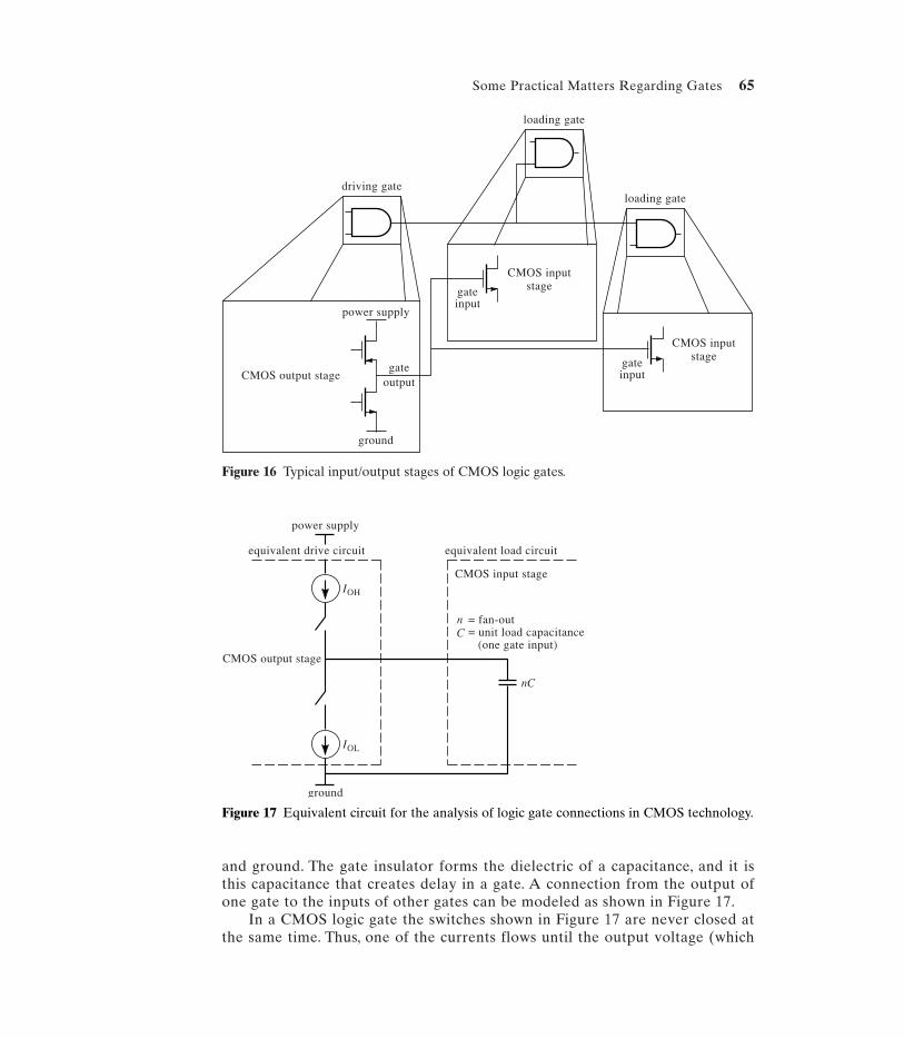
Some Practical Matters Regarding Gates 65
and ground. The gate insulator forms the dielectric of a capacitance, and it isthis capacitance that creates delay in a gate. A connection from the output ofone gate to the inputs of other gates can be modeled as shown in Figure 17.
In a CMOS logic gate the switches shown in Figure 17 are never closed atthe same time. Thus, one of the currents flows until the output voltage (which
Figure 16 Typical input/output stages of CMOS logic gates.
CMOS output stage
CMOS inputstage
driving gate
loading gate
CMOS inputstage
loading gate
power supply
gateoutput
gateinput
ground
gateinput
CMOS output stage
CMOS input stage
equivalent drive circuit
power supply
ground
equivalent load circuit
IOL
nC
IOH
nC
= fan-out= unit load capacitance (one gate input)
Figure 17 Equivalent circuit for the analysis of logic gate connections in CMOS technology.
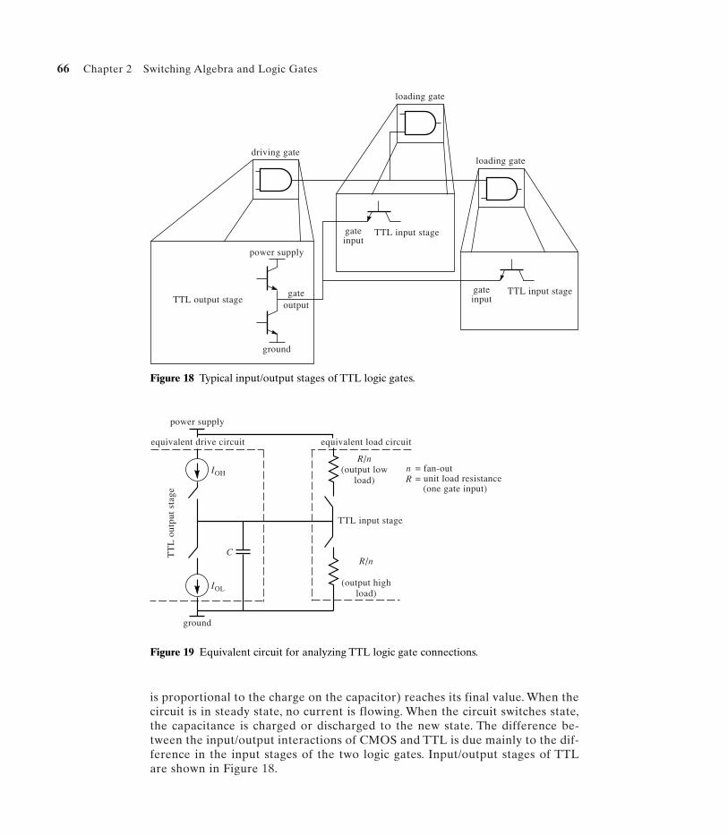
66 Chapter 2 Switching Algebra and Logic Gates
is proportional to the charge on the capacitor) reaches its final value. When thecircuit is in steady state, no current is flowing. When the circuit switches state,the capacitance is charged or discharged to the new state. The difference be-tween the input/output interactions of CMOS and TTL is due mainly to the dif-ference in the input stages of the two logic gates. Input/output stages of TTLare shown in Figure 18.
TTL output stage
loading gate
driving gate
TTL input stage
loading gate
power supply
ground
gateoutput
gateinput
gateinput
TTL input stage
Figure 18 Typical input/output stages of TTL logic gates.
Figure 19 Equivalent circuit for analyzing TTL logic gate connections.
TT
L o
utpu
t st
age
TTL input stage
equivalent drive circuit
power supply
ground
equivalent load circuit
IOL
C
IOH
R/n(output low
load)
R/n
(output highload)
nR
= fan-out= unit load resistance (one gate input)
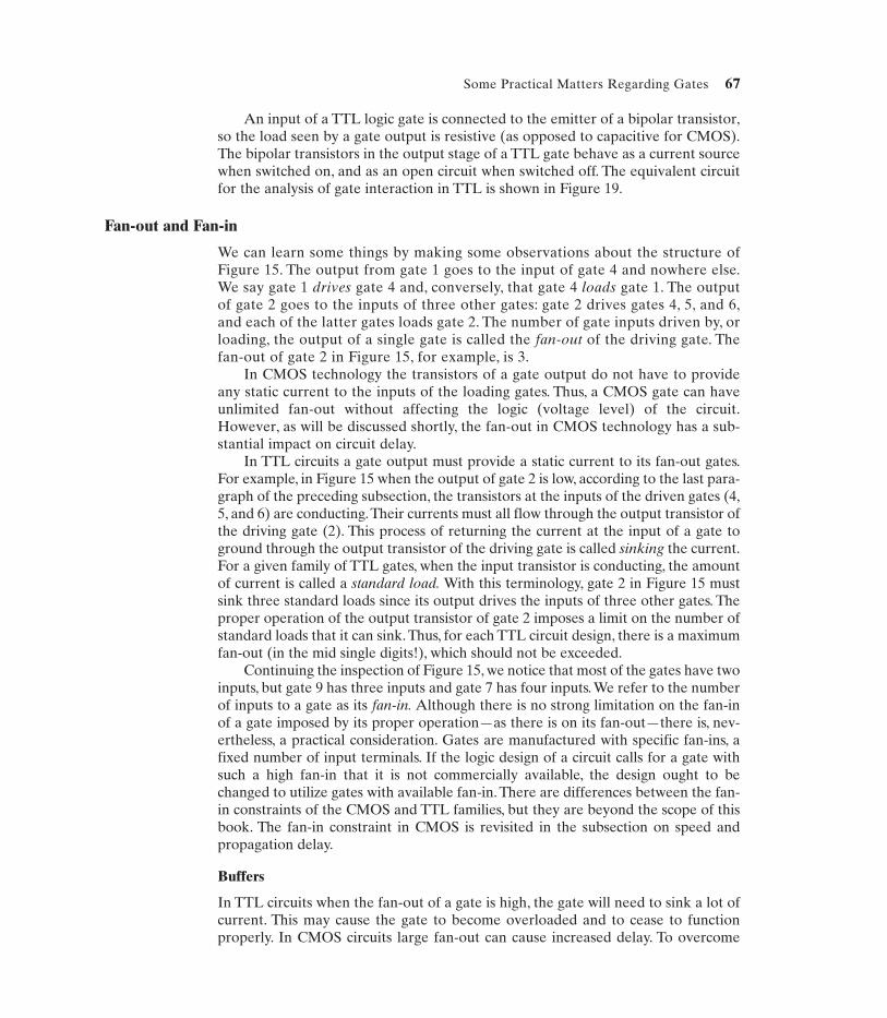
Some Practical Matters Regarding Gates 67
An input of a TTL logic gate is connected to the emitter of a bipolar transistor,so the load seen by a gate output is resistive (as opposed to capacitive for CMOS).The bipolar transistors in the output stage of a TTL gate behave as a current sourcewhen switched on, and as an open circuit when switched off. The equivalent circuitfor the analysis of gate interaction in TTL is shown in Figure 19.
Fan-out and Fan-in
We can learn some things by making some observations about the structure ofFigure 15. The output from gate 1 goes to the input of gate 4 and nowhere else.We say gate 1 drives gate 4 and, conversely, that gate 4 loads gate 1. The outputof gate 2 goes to the inputs of three other gates: gate 2 drives gates 4, 5, and 6,and each of the latter gates loads gate 2. The number of gate inputs driven by, orloading, the output of a single gate is called the fan-out of the driving gate. Thefan-out of gate 2 in Figure 15, for example, is 3.
In CMOS technology the transistors of a gate output do not have to provideany static current to the inputs of the loading gates. Thus, a CMOS gate can haveunlimited fan-out without affecting the logic (voltage level) of the circuit.However, as will be discussed shortly, the fan-out in CMOS technology has a sub-stantial impact on circuit delay.
In TTL circuits a gate output must provide a static current to its fan-out gates.For example, in Figure 15 when the output of gate 2 is low, according to the last para-graph of the preceding subsection, the transistors at the inputs of the driven gates (4,5, and 6) are conducting.Their currents must all flow through the output transistor ofthe driving gate (2). This process of returning the current at the input of a gate toground through the output transistor of the driving gate is called sinking the current.For a given family of TTL gates, when the input transistor is conducting, the amountof current is called a standard load. With this terminology, gate 2 in Figure 15 mustsink three standard loads since its output drives the inputs of three other gates. Theproper operation of the output transistor of gate 2 imposes a limit on the number ofstandard loads that it can sink.Thus, for each TTL circuit design, there is a maximumfan-out (in the mid single digits!), which should not be exceeded.
Continuing the inspection of Figure 15, we notice that most of the gates have twoinputs, but gate 9 has three inputs and gate 7 has four inputs. We refer to the numberof inputs to a gate as its fan-in. Although there is no strong limitation on the fan-inof a gate imposed by its proper operation—as there is on its fan-out—there is, nev-ertheless, a practical consideration. Gates are manufactured with specific fan-ins, afixed number of input terminals. If the logic design of a circuit calls for a gate withsuch a high fan-in that it is not commercially available, the design ought to bechanged to utilize gates with available fan-in. There are differences between the fan-in constraints of the CMOS and TTL families, but they are beyond the scope of thisbook. The fan-in constraint in CMOS is revisited in the subsection on speed andpropagation delay.
Buffers
In TTL circuits when the fan-out of a gate is high, the gate will need to sink a lot ofcurrent. This may cause the gate to become overloaded and to cease to functionproperly. In CMOS circuits large fan-out can cause increased delay. To overcome
these difficulties, a (noninverting) buffer is introduced at the output of the gate; itsfunction is simply to provide increased drive current that permits continued opera-tion with an increased load. The buffer performs no logical operation except thetrivial identity operation. That is, its output is the same as its input. The logic symbolfor the buffer is shown in Figure 20a; it is an inverter without the bubble. It mightbe made up of two cascaded inverters, as shown in Figure 20b. In this way, both avariable and its complement are available to drive a substantial load.
Power Consumption
Whenever there is current in a physical circuit, some of the associated electri-cal power will be converted to heat. If the circuit is to continue functioning, thisheat must be dissipated so as not to result in excessive heating of the devices inthe circuit. The design of gates and integrated circuits—including power-supplyrequirements, the number and type of transistors, and other factors—will havea lot to do with the power consumption. It is possible to design circuits specifi-cally for low power consumption. You must know by now, however, that youcan’t get something for nothing. Low power consumption can be achieved at aprice—usually at the expense of reduced speed. Review the tables for the TTLfamily in Figure 13 and the CMOS family in Figure 14; notice the range ofpower dissipation based on the variety of designs.
Noise Margin
Each logic family has specific nominal voltages corresponding to its high leveland its low level. (For the TTL family, the nominal high value is 3.3 V and thenominal low value is 0.5 V.) However, digital circuits operate reliably evenwhen actual voltage levels deviate considerably from their nominal values.Moreover, the high output level of a gate is not necessarily the same as its highinput level. What is considered a “high” input or output voltage must extendover a range of values and similarly for “low” values.
The inputs and outputs of the gates under discussion are signals that we in-tend them to have. But there are many ways in which unwanted signals can begenerated in a circuit and thus change input and output values from what areintended. We refer to such extraneous signals produced in a system as noise.Noise can be generated by a variety of mechanisms within the environment inwhich a circuit operates, from atmospheric radiation to interference from the60 Hz power system. Noise can also be generated within the electronic devicesin the system itself.
When intended signals are accompanied by noise, the actual signals will bemodified versions of the desired ones. Provision must be made in the design ofthe circuit to enable it to continue to operate in the presence of noise up tosome anticipated level. That is, there should be a certain immunity to noise. A
68 Chapter 2 Switching Algebra and Logic Gates
Figure 20 Buffer.(b)(a)
measure of the amount of noise that will be tolerated before a circuit malfunc-tions is the noise margin, N. We will not pursue the details of this topic. Sufficeit to say that what are considered high voltage levels and low voltage levels inthe operation of gates are not fixed values but ranges of values. So long as inputand output voltages stay within the range of values specified by the manufac-turer, even though contaminated by noise, the gates will operate as if the volt-ages had their nominal values.
Speed and Propagation Delay
The speed at which logic circuits operate determines how rapidly they completea task. Limitations on the speed arise from two sources:
• The delay encountered by a signal in going through a single gate • The number of levels in the circuit, that is, the number of gates a signal en-
counters in going from an input to the output. We call the sequence of gatesfrom an input to an output in a circuit a logic path.
Exercise 16 Reexamine Figure 15. Specify the number of levels that eachinput encounters on its way to the output.Answer19
The delay in a TTL gate stems largely from the fact that transistors withinthe gate require a nonzero time to switch from a cut off state to a conductingcondition and vice versa. This delay, for the most part, is independent of theload seen by a gate. Thus, in TTL circuits it can be assumed that a gate has afixed delay, and the total delay from a logic input to a logic output can be esti-mated by accumulating the delays of the gates in the logic path from input tooutput.
The delay in a CMOS gate comes not only from the time required for tran-sistors to switch between conducting and nonconducting states, but also fromthe time required to charge and discharge the load capacitance of the fan-outgates. Let’s call the delay due to the switching of state of the transistors in agate the intrinsic delay of a gate, and the delay due to load capacitance the ex-trinsic delay. The intrinsic delay is a strong function of the fan-in of a gate; theextrinsic delay is a strong function of its fan-out. Gates with large fan-in have agreater intrinsic delay than gates with small fan-in.
In CMOS it can be advantageous to increase the number of gate levels tokeep the fan-in low in order to decrease the delay of a circuit. For example,three realizations of an eight-input AND gate are shown in Figure 21. In CMOStechnology (due to the characteristics of the MOSFET) it is likely that the re-alizations shown in Figures 21b and 21c have lower delays than the one inFigure 21a; this, however, depends on the characteristics of the specific sub-family of CMOS used for the implementation. The extrinsic delay is caused by
Some Practical Matters Regarding Gates 69
19Six signals encounter the maximum of four levels, one signal encounters three levels, and two signalsencounter one level. �
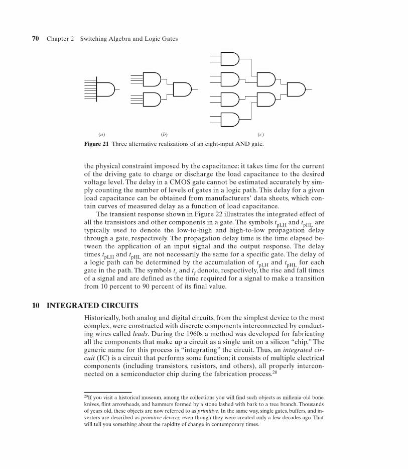
the physical constraint imposed by the capacitance: it takes time for the currentof the driving gate to charge or discharge the load capacitance to the desiredvoltage level. The delay in a CMOS gate cannot be estimated accurately by sim-ply counting the number of levels of gates in a logic path. This delay for a givenload capacitance can be obtained from manufacturers’ data sheets, which con-tain curves of measured delay as a function of load capacitance.
The transient response shown in Figure 22 illustrates the integrated effect ofall the transistors and other components in a gate. The symbols tpLH and tpHL aretypically used to denote the low-to-high and high-to-low propagation delaythrough a gate, respectively. The propagation delay time is the time elapsed be-tween the application of an input signal and the output response. The delaytimes tpLH and tpHL are not necessarily the same for a specific gate. The delay ofa logic path can be determined by the accumulation of tpLH and tpHL for eachgate in the path. The symbols tr and tf denote, respectively, the rise and fall timesof a signal and are defined as the time required for a signal to make a transitionfrom 10 percent to 90 percent of its final value.
10 INTEGRATED CIRCUITS
Historically, both analog and digital circuits, from the simplest device to the mostcomplex, were constructed with discrete components interconnected by conduct-ing wires called leads. During the 1960s a method was developed for fabricatingall the components that make up a circuit as a single unit on a silicon “chip.” Thegeneric name for this process is “integrating” the circuit. Thus, an integrated cir-cuit (IC) is a circuit that performs some function; it consists of multiple electricalcomponents (including transistors, resistors, and others), all properly intercon-nected on a semiconductor chip during the fabrication process.20
70 Chapter 2 Switching Algebra and Logic Gates
20If you visit a historical museum, among the collections you will find such objects as millenia-old boneknives, flint arrowheads, and hammers formed by a stone lashed with bark to a tree branch. Thousandsof years old, these objects are now referred to as primitive. In the same way, single gates, buffers, and in-verters are described as primitive devices, even though they were created only a few decades ago. Thatwill tell you something about the rapidity of change in contemporary times.
Figure 21 Three alternative realizations of an eight-input AND gate.
(c)(b)(a)
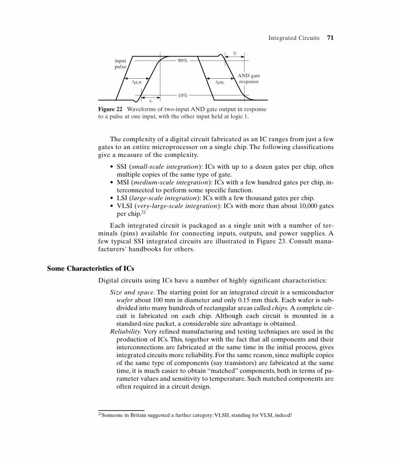
Integrated Circuits 71
Figure 22 Waveforms of two-input AND gate output in responseto a pulse at one input, with the other input held at logic 1.
tpLH tpHL
tr
inputpulse
90%
10%
AND gateresponse
tf
The complexity of a digital circuit fabricated as an IC ranges from just a fewgates to an entire microprocessor on a single chip. The following classificationsgive a measure of the complexity.
• SSI (small-scale integration): ICs with up to a dozen gates per chip, oftenmultiple copies of the same type of gate.
• MSI (medium-scale integration): ICs with a few hundred gates per chip, in-terconnected to perform some specific function.
• LSI (large-scale integration): ICs with a few thousand gates per chip.• VLSI (very-large-scale integration): ICs with more than about 10,000 gates
per chip.21
Each integrated circuit is packaged as a single unit with a number of ter-minals (pins) available for connecting inputs, outputs, and power supplies. Afew typical SSI integrated circuits are illustrated in Figure 23. Consult manu-facturers’ handbooks for others.
Some Characteristics of ICs
Digital circuits using ICs have a number of highly significant characteristics:
Size and space. The starting point for an integrated circuit is a semiconductorwafer about 100 mm in diameter and only 0.15 mm thick. Each wafer is sub-divided into many hundreds of rectangular areas called chips. A complete cir-cuit is fabricated on each chip. Although each circuit is mounted in astandard-size packet, a considerable size advantage is obtained.
Reliability. Very refined manufacturing and testing techniques are used in theproduction of ICs. This, together with the fact that all components and theirinterconnections are fabricated at the same time in the initial process, givesintegrated circuits more reliability. For the same reason, since multiple copiesof the same type of components (say transistors) are fabricated at the sametime, it is much easier to obtain “matched” components, both in terms of pa-rameter values and sensitivity to temperature. Such matched components areoften required in a circuit design.
21Someone in Britain suggested a further category: VLSII, standing for VLSI, indeed!
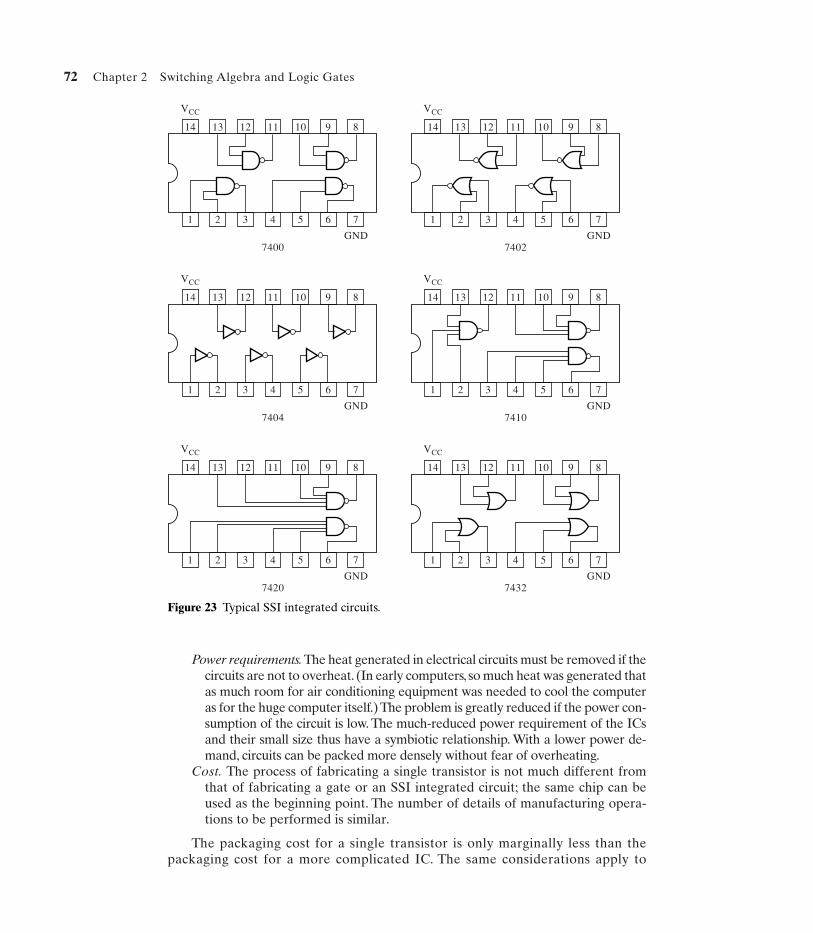
Power requirements. The heat generated in electrical circuits must be removed if thecircuits are not to overheat. (In early computers, so much heat was generated thatas much room for air conditioning equipment was needed to cool the computeras for the huge computer itself.) The problem is greatly reduced if the power con-sumption of the circuit is low. The much-reduced power requirement of the ICsand their small size thus have a symbiotic relationship. With a lower power de-mand, circuits can be packed more densely without fear of overheating.
Cost. The process of fabricating a single transistor is not much different fromthat of fabricating a gate or an SSI integrated circuit; the same chip can beused as the beginning point. The number of details of manufacturing opera-tions to be performed is similar.
The packaging cost for a single transistor is only marginally less than thepackaging cost for a more complicated IC. The same considerations apply to
72 Chapter 2 Switching Algebra and Logic Gates
VCC
GND7400
14 13 12 11 10 9 8
1 2 3 4 5 6 7
VCC
GND7402
14 13 12 11 10 9 8
21 3 4 5 6 7
VCC
GND7404
14 13 12 11 10 9 8
1 2 3 4 5 6 7
VCC
GND7410
14 13 12 11 10 9 8
21 3 4 5 6 7
VCC
GND7420
14 13 12 11 10 9 8
1 2 3 4 5 6 7
VCC
GND7432
14 13 12 11 10 9 8
21 3 4 5 6 7
Figure 23 Typical SSI integrated circuits.
two different ICs with different numbers of gates: the cost of an IC with 30–40gates is only slightly lower than the cost for one with 80–90 gates. Thus, the costof an IC is not directly proportional to the number of individual componentspacked in a package; steps in the manufacturing process cost only marginallymore if the number of gates in the package is doubled, for example.
Design Economy
When logic circuits were constructed with discrete (“primitive”) gates, costs could bereduced by reducing the number of gates required to perform a particular function.Procedures for finding such minimal circuits became very highly developed. Suchminimization procedures still play a role, especially in connection with logic designusing what are called programmable logic devices (PLDs), as we will see in Chapters4 and 8. We will therefore devote some attention to them in the following chapter.
The cost of a circuit designed with SSI ICs, however, depends not simply onthe gate count but also on the IC package count.22 Thus, adding a gate or twoto a design may cost nothing extra if SSI packages with unused gates are al-ready present in the design. Or suppose that a particular task can be achievedwith a 25-gate circuit in two SSI packages, and a 40-gate package (with gateshaving the appropriate number of inputs) is available; it might be less costly touse the single package in the design and “waste” the unused gates rather thanusing the two packages with fewer gates.
In some cases another part of the circuit to be designed may call for a fewgates of the kind left unused in the design just described. These previously“wasted” gates could now be used for this purpose, with no further hardwarecost except for the cost of making pin connections, something that would be re-quired anyway. In any case, design economy no longer depends on gate countbut on integrated circuit package count and of the number of connections thathave to be made in constructing the circuit.
One way in which to economize on package count, for example, is to avoidusing inverters (e.g., 74LS04s). Instead, use an available fraction of a NAND,NOR, or XOR package. Consider the following expressions:
A' = (A + A + ... + A)' = (A + 0 + ... + 0)' (25)
A' = (A•A• ... •A)' = (A•1• ... •1)' (26)
A' = A ⊕ 1 (27)
From (26) we note that the complement of a variable is the output of a NANDgate with any number of inputs all connected to that variable, or one input con-nected to that variable and all the rest connected to a high voltage (logic 1, as-suming positive logic). Thus, if one-quarter of a 74LS00 (or one-third of a74LS10) is unused in a package whose remainder already forms part of a cir-cuit, this fraction of the package can be used to implement an inverter at no fur-ther hardware cost.
Integrated Circuits 73
22In practice, multiple chips in a design are mounted on a printed-circuit board (PCB). So design econ-omy involves not only the IC count but the PCB count as well. Such practical matters are easily learnedwhen one is engaged in practice and need not concern us here.
Exercise 17 In a similar way, interpret the expressions in (25) and (27) for im-plementing an inverter. �
As we shall see in Chapter 4, many combinational-circuit units that performsome rather complex functions have been available for some time in MSI inte-grated circuits. There is no longer any need to design such functions by com-bining individual gates in SSI packages.
Application-Specific ICs
The integrated circuits and chips discussed so far have been general purpose.The SSI chips illustrated in Figure 23, for example, the MSI chips in which theapplications to be described in Chapter 4 are implemented, or even the LSIchips that embody larger units can be used in the design of a wide variety of ap-plications. A more recent development is the possibility of designing a chip forone particular application. If only a few of the resulting chips will ever be used,then it would make no economic sense to spend the required engineering de-sign resources. On the other hand, if the number of copies needed is large, itmay be economically feasible to design an entire integrated circuit just for thisparticular application. It should be no surprise that this type of IC is called anapplication-specific integrated circuit (ASIC).
Two kinds of costs are associated with an ASIC. Once the unit is designedand debugged, there will be production costs. Of course, the actual design anddebugging itself will entail a substantial cost, but this will not depend on laterproduction costs; it is a nonrecurrent engineering (NRE) cost. Why undertakean enterprise requiring high NRE costs unless there is some cost or perfor-mance advantage? Indeed, ASICs do provide such advantages: generally, thesystem uses use fewer chips, has smaller physical size, and consequently lowerpower consumption and smaller time delays, and thus smaller delay-powerproducts. We will not pursue this topic any further.
11 WIRED LOGIC
It is sometimes convenient to perform logic functions using special circuit con-figurations and connections rather than logic gates (for example, simply by con-necting two or more wires together). Two types of gates are described in thissection that enable the use of such special configurations and connections. Theusefulness of these gates is probably not obvious to you at this point, but it willbe when we get to Chapter 4. We consider them here because their implemen-tation depends on the transistor circuits described in the previous section.
Tristate (High-Impedance) Logic Gates
Consider the equivalent circuit for the output stage of a CMOS gate as shown inFigure 16. In a conventional CMOS gate the logic inputs to the gate control thestate of the switches (the output transistors). For example, in a two-input NANDgate the switch between the output and ground is closed if both inputs are logic1; otherwise the switch between the output and the power supply is closed. The
74 Chapter 2 Switching Algebra and Logic Gates
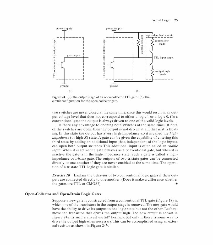
two switches are never closed at the same time, since this would result in an out-put voltage level that does not correspond to either a logic 1 or a logic 0. (In aconventional gate the output is always driven to one of the valid logic levels.
Is there any advantage to opening both switches at the same time? If bothof the switches are open, then the output is not driven at all; that is, it is float-ing. In this state the output has a very high impedance, so it is called the high-impedance (or high-Z) state. A gate can be given the capability of entering thisthird state by adding an additional input that, independent of the logic inputs,can open both output switches. This additional input is often called an enableinput. When it is active the gate behaves as a conventional gate, but when it isinactive the gate is in the high-impedance state. Such a gate is called a high-impedance or tristate gate. The outputs of two tristate gates can be connecteddirectly to one another if they are never enabled at the same time. The opera-tion of a tristate TTL logic gate is similar.
Exercise 18 Explain the behavior of two conventional logic gates if their out-puts are connected directly to one another. (Does it make a difference whetherthe gates are TTL or CMOS?) �
Open-Collector and Open-Drain Logic Gates
Suppose a new gate is constructed from a conventional TTL gate (Figure 18) inwhich one of the transistors in the output stage is removed. The new gate wouldhave the ability to drive its output to one logic state but not the other. Let’s re-move the transistor that drives the output high. The new circuit is shown inFigure 24a. Is such a circuit useful? Perhaps, but only if there is some way todrive the output high when necessary. This can be accomplished using an exter-nal resistor as shown in Figure 24b.
Wired Logic 75
Figure 24 (a) The output stage of an open-collector TTL gate. (b) Thecircuit configuration for the open-collector gate.
equivalent load circuit
power supply
gate outputT
TL
ope
n-co
llec
tor
outp
ut s
tage
ground
(a)
power supply
TT
L o
pen-
coll
ecto
r ou
tput
sta
ge
exte
rnal
res
isto
r
ground
(b)
TTL input stage
(output lowload)
(output highload)
When the inputs of the gate are such that the output is driven low, it is dri-ven low through the TTL gate output; the resistor acts as an additional load inparallel with the fan-out gates. The resistance value must not be so small that itoverloads the gate. When the inputs are such that the output should be drivenhigh, the ouput is not driven by the TTL gate; the external resistor provides apath for current to drive the fan-out gates instead.
Notice that when the output is driven high, the external resistor is in serieswith the equivalent input stages of the fan-out gates; thus, its value should be cho-sen such that an output voltage corresponding to a valid logic level is achieved.This kind of gate is called an open-collector gate because the collector of the out-put transistor is an open circuit without any internal connection on the chip. Asimilar gate can be constructed in CMOS and is called an open-drain gate because,internal to the chip, the drain terminal of the output transistor is not connected.
The usefulness of this circuit is not obvious. Furthermore, we need more compo-nents than we started with (an external resistor). However, if we connect the outputsof two or more such gates, we have a circuit that always provides a valid logic level aslong as the external resistor has an appropriate value. If one or more of the gates pullthe output low, then the external resistor acts as an additional load. If none of thegates pull the output low, then the external resistor provides a conductive path for cur-rent and drives the output high. For this reason the connection is called a wired-AND.If one or more of the outputs wired together correspond to a logic 0, then, assumingpositive logic, the signal does likewise; otherwise, it corresponds to a logic 1.
CHAPTER SUMMARY AND REVIEW
This chapter introduced Boolean algebra and the results that follow from itsuse. It also introduced the primitive devices, called gates, on which logic designis based. The following topics were included.
• Huntington’s postulates• Boolean algebra
• Involution• Idempotency• Absorption• Associative law• Consensus
• De Morgan’s law• Switching operations: AND, OR, NOT, NAND, NOR, XOR, XNOR• Switching expressions
• Sum-of-products form• Product-of-sums form• Canonic form
• Minterms and maxterms• Switching functions• Shannon’s expansion theorem: s-of-p and p-of-s• Universal operations
76 Chapter 2 Switching Algebra and Logic Gates
• Logic gates• Equivalent forms of NAND and NOR gates• Positive, negative, and mixed logic• Families of logic gates: TTL, CMOS• Gate properties
• Fan-out• Fan-in• Power consumption• Propagation delay• Speed• Noise margin
• Integrated circuits: SSI, MSI, LSI, VLSI, ASIC• Wired logic
• Tristate gates• Open-collector gates• Open-drain gates.
PROBLEMS
1 Prove the following theorems of Boolean algebra.
a. The identity elements are distinct; that is, they are not the same.b. The identity elements are unique; that is, there are no others.c. The inverse of an element is unique; that is, there aren’t two different inverses.d. The complement of an element is unique. From this, prove (x')' = x.
2 Use the distributive law and any other laws of switching algebra to place each of the follow-ing expressions in simplest sum-of-products form. (These are useful results to remember.)
a. f1 = (A + B)(A + C)b. f2 = (A + B)(A' + C)
3 Complete the details of the proof of the associative law (Theorem 6) outlined in the text.4 Prove the consensus theorem by perfect induction, that is, by showing it to be true for allpossible values of the variables.5 Prove that a Boolean algebra of three distinct elements, say {0, 1, 2}, does not exist. (If allof Huntington’s postulates were satisfied, then it would exist.)6 The following set of four elements is under consideration as the elements of a Boolean al-gebra: {0, 1, a, b}. The identity elements that satisfy Postulate 2 are to be 0 and 1. Fill in the ta-bles for (+) and (•) in Figure P6 such that the algebraic system defined by these tables will bea Boolean algebra. Find the complement of each element, and confirm that all ofHuntington’s postulates are satisfied.7 The operations of a four-element algebraic system are given in Figure P7. Determinewhether this system is a Boolean algebra. If so, which are the identity elements?8 In a natural-food restaurant, fruit is offered for dessert but only in certain combinations.One choice is either peaches or apples or both. Another choice is either cherries and applesor neither. A third choice is peaches, but if you choose peaches, then you must also take ba-nanas. Define Boolean variables for all of the fruits and write a logical expression that spec-ifies the fruit available for dessert. Then simplify the expression.9 Write a logical expression that represents the following proposition: The collector currentin a bipolar transistor is proportional to the base-emitter voltage vBE, provided the transistoris neither saturated nor cut off.
Problems 77
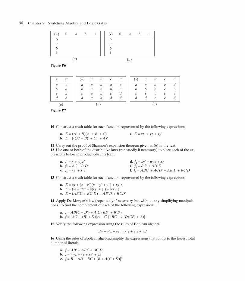
10 Construct a truth table for each function represented by the following expressions.
a. E = (A' + B)(A' + B' + C) c. E = xz' + yz + xy'b. E = (((A' + B)' + C)' + A)'
11 Carry out the proof of Shannon’s expansion theorem given as (6) in the text.12 Use one or both of the distributive laws (repeatedly if necessary) to place each of the ex-pressions below in product-of-sums form.
a. f1 = x + wyz' d. f4 = xy' + wuv + xzb. f2 = AC + B'D' e. f5 = BC' + AD'Ec. f3 = xy' + x'y f. f6 = ABC' + ACD' + AB'D + BC'D
13 Construct a truth table for each function represented by the following expressions.
a. E = xy + (x + z')(x + y' + z') + xy'zb. E = (w + x'z' + y)(y' + z') + wxy'zc. E = (AB'C + BC'D) + AB'D + BCD'
14 Apply De Morgan’s law (repeatedly if necessary, but without any simplifying manipula-tions) to find the complement of each of the following expressions.
a. f = AB(C + D') + A'C'(BD' + B'D)b. f = [AC' + (B' + D)(A + C')][BC + A'D(CE' + A)]
15 Verify the following expression using the rules of Boolean algebra.
x'y + y'z + yz' = x'z + y'z + yz'
16 Using the rules of Boolean algebra, simplify the expressions that follow to the fewest totalnumber of literals.
a. f = AB' + ABC + AC'Db. f = wyz + xy + xz' + yzc. f = B + AD + BC + [B + A(C + D)]'
78 Chapter 2 Switching Algebra and Logic Gates
(+) 0 a b 1
0ab1
(•) 0 a b 1
0ab1
(a) (b)
Figure P6
(a) (b) (c)
x x'
a cb dc ad b
(+) a b c d
a a a a ab a b b ac a b c dd a a d d
(•) a b c d
a a b c db b b c cc c c c cd d c c d
Figure P7
17 Use switching algebra to simplify the following expressions as much as possible.
a. xyz' + xy'z' + x'yb. (wx')'(w + y)(x'y'z')'c. x'(y + wy'z') + x'y'(w'z' + z)d. (w + x)(w' + x + yz')(w + y')
18 a. Carry out appropriate switching operations on the following expressions to arriveat noncanonic sum-of-products forms. Then restore missing variables to convertthem to canonic form.
b. In each case, using the distributive law and other Boolean laws, convert the non-canonic sum-of-products form to product-of-sums form.
c. In each case, restore the missing variables to the forms determined in part a to con-vert them to canonic form.
d. In each case, construct the truth table and confirm the canonic sum-of-productsform.
e. In each case, by applying De Morgan’s law to the complements of the minterms ab-sent from the canonic sum-of-products form, find the canonic product-of-sumsform.
E1 = (x + y')(y + z')
E2 = (x'y + x'z)'
E3 = (x + yz')(y + xz')
E4 = (B + D')(A + D')(B' + D')
E5 = (AB)'(B + C'D)(A + D')
19 Use switching algebra to prove the following relationships.
a. x' ⊕ y = x ⊕ y'b. x' ⊕ y' = x ⊕ yc. x'y ⊕ xy' = x ⊕ y
20 Use appropriate laws of switching algebra to convert the expression (x ⊕ y)(x ⊕ z) to theform A ⊕ B; specify A and B in terms of x, y, z.21 a. Express the Exclusive-OR function, x ⊕ y, in terms of only NAND functions.
b. Express x ⊕ y in terms of only NOR functions.
22 Prove that the Exclusive-OR operation is associative. That is, (x ⊕ y) ⊕ z = x ⊕ (y ⊕ z).23 Show that {NOR} is a universal set of operations.24 The implication function f = (x ⇒ y) is the statement “If x is true, then y is true.”A switch-ing expression for the implication function is f = x' + y. This function can be implemented bya two-input OR gate in which one of the input lines has a bubble. It might be called an im-plication gate.
a. Construct a truth table for the implication function. Are any of the rows puzzling?b. Show that the implication function constitutes a universal set; that is, any switching
expression can be represented in terms of implication functions only.c. Write the following expression in terms of implication functions only: f = AC + BC'.
25 Each of the following expressions includes all three of the Boolean operations. Using ap-propriate Boolean theorems, convert each expression to one that includes
a. Only AND and NOT operationsb. Only OR and NOT operations
Problems 79
c. Only NAND operationsd. Only NOR operations
E1 = AB' + AC + B'C
E2 = (x' + y')(y' + z)(y + z')
E3 = xy' + (y + z')(x + z)
26 a. Use the result of Figure 2 in the text to convert a two-level AND-OR circuit con-sisting of two double-input AND gates followed by an OR gate into an all-NANDcircuit.
b. Use the result of Exercise 15 in the text to convert a two-level OR-AND circuitconsisting of two double-input OR gates followed by an AND gate into an all-NORcircuit.
27 Show that the OR operation in the first form of Shannon’s theorem can be replaced bythe Exclusive-OR.28 Determine the relationship between the Exclusive-OR function and its dual.29 The objective of this problem is to convert one kind of two-input gate to a different kindof gate but with inverted inputs. Let the inputs be A and B. Use an appropriate Boolean the-orem to carry out this objective for the following gate types:
AND: ABOR: A + BNAND: (AB)'NOR: (A + B)'
30 An OR gate has two inputs A and B. B is obtained from A after A goes through three con-secutive inverters. Assume that each inverter has a 1 µs delay. Suppose that A has been 1 forsome time and then drops to 0. Draw the waveform of the resulting output.31 A standard load for an LS-TTL gate is 3 mA of current; such a gate can drive three stan-dard loads of the same kind of gate. A standard load for an S-TTL gate is 7mA. How manyS-TTL gates can be driven by an LS-TTL gate?32 Assuming the logic-high and logic-low voltage levels of two CMOS and TTL subfamiliesare compatible, what are the consequences of driving a TTL gate with a CMOS gate and viceversa?33 The intrinsic delay of a gate is 0.5 ns and the extrinsic delay is 0.2 ns per load. What is thefan-out limitation of this gate, given that its delay cannot exceed 1.2 ns?34 Can the outputs of conventional gates be connected to the outputs of open-collectorgates? If so, show such a circuit and describe its operation. If not, explain why they cannot beconnected together.35 What is the consequence of connecting many tristate outputs together? How many tri-state outputs can be connected without affecting the proper functionality of a circuit? 36 What is the consequence of connecting many open-collector outputs together? Howmany open-collector outputs can be connected without affecting the proper functionality ofa circuit?37 Can the outputs of open-collector and tristate gates be connected together? Explain whyor why not.
80 Chapter 2 Switching Algebra and Logic Gates