
Switch Including IGBT and a Rapid Switching Diode
17
energies Article Electrothermal Averaged Model of a Diode-Transistor Switch Including IGBT and a Rapid Switching Diode Pawel Górecki and Krzysztof Górecki * Department of Marine Electronics, Gdynia Maritime University, Morska 83, 81-225 Gdynia, Poland; [email protected] * Correspondence: [email protected] Received: 18 May 2020; Accepted: 10 June 2020; Published: 12 June 2020 Abstract: This study proposes an electrothermal averaged model of the diode–transistor switch including insulated gate bipolar transistor (IGBT) and a rapid switching diode. The presented model has the form of subcircuits dedicated for simulation program with integrated circuit emphasis (SPICE) and it makes it possible to compute characteristics of DC–DC converters at the steady state considering self-heating phenomena, both in the diode and in IGBT. This kind of model allows computations of voltages, currents and internal temperatures of all used semiconductor devices at the steady state. The formulas used in this model are adequate for both: continuous conducting mode (CCM) and discontinuous conducting mode (DCM). Correctness of the proposed model is verified experimentally for a boost converter including IGBT. Good accuracy in modeling these converter characteristics is obtained. Keywords: IGBT; DC–DC converter; electrothermal model; averaged model; thermal phenomena; self-heating; diode–transistor switch; power electronics 1. Introduction Nowadays, power electronic circuits often include DC–DC converters [1–5]. Designing these converters requires reliable methods of computer simulations [1,5,6]. They enable selection of optimal components and operating conditions of the designed converter. For more than 50 years, many scientists have been working on methods and models that allow fast computations of waveforms of currents and voltages as well as AC and DC characteristics of power converters [5–8]. To provide simulations of electronic circuits using the formulated models it is necessary to use software dedicated to electronic circuits simulation. SPICE (simulation program with integrated circuit emphasis) is commonly used for this purpose [5,6,8–10]. Its main advantage is easy implementation of any compact model of electronic components and devices. Due to the switching mode of operation of DC–DC converters, their characteristics can be obtained with the sequential analysis of transient processes only. Such analysis requires, as a rule, a long time—and may cause convergence problems of computations [11]. In order to shorten the time of this analysis, the averaged models of DC–DC converters were proposed [5,8,12–15]. These models make it possible to compute characteristics of circuits at the steady state using a DC sweep (DC analysis) [5,8,16]. This is one of the types of the standard analyses realized in SPICE. Typically, a DC analysis needs a short computation time. In averaged models, the average values of voltages in nodes and currents flowing through branches of considered circuits are used instead of the instantaneous values of these quantities. It is assumed that averaged DC–DC converters models should be formulated in accordance with two steps of their activation in “on” and “off” phases of a switch. In the first step, the transistor is turned on, and simultaneously the diode is turned off. In the second step, the transistor is turned off Energies 2020, 13, 3033; doi:10.3390/en13123033 www.mdpi.com/journal/energies
Transcript of Switch Including IGBT and a Rapid Switching Diode

energies
Article
Electrothermal Averaged Model of a Diode-TransistorSwitch Including IGBT and a Rapid Switching Diode
Paweł Górecki and Krzysztof Górecki *
Department of Marine Electronics, Gdynia Maritime University, Morska 83, 81-225 Gdynia, Poland;[email protected]* Correspondence: [email protected]
Received: 18 May 2020; Accepted: 10 June 2020; Published: 12 June 2020
Abstract: This study proposes an electrothermal averaged model of the diode–transistor switchincluding insulated gate bipolar transistor (IGBT) and a rapid switching diode. The presented modelhas the form of subcircuits dedicated for simulation program with integrated circuit emphasis (SPICE)and it makes it possible to compute characteristics of DC–DC converters at the steady state consideringself-heating phenomena, both in the diode and in IGBT. This kind of model allows computations ofvoltages, currents and internal temperatures of all used semiconductor devices at the steady state.The formulas used in this model are adequate for both: continuous conducting mode (CCM) anddiscontinuous conducting mode (DCM). Correctness of the proposed model is verified experimentallyfor a boost converter including IGBT. Good accuracy in modeling these converter characteristicsis obtained.
Keywords: IGBT; DC–DC converter; electrothermal model; averaged model; thermal phenomena;self-heating; diode–transistor switch; power electronics
1. Introduction
Nowadays, power electronic circuits often include DC–DC converters [1–5]. Designing theseconverters requires reliable methods of computer simulations [1,5,6]. They enable selection of optimalcomponents and operating conditions of the designed converter. For more than 50 years, many scientistshave been working on methods and models that allow fast computations of waveforms of currentsand voltages as well as AC and DC characteristics of power converters [5–8]. To provide simulationsof electronic circuits using the formulated models it is necessary to use software dedicated to electroniccircuits simulation. SPICE (simulation program with integrated circuit emphasis) is commonly used forthis purpose [5,6,8–10]. Its main advantage is easy implementation of any compact model of electroniccomponents and devices.
Due to the switching mode of operation of DC–DC converters, their characteristics can be obtainedwith the sequential analysis of transient processes only. Such analysis requires, as a rule, a longtime—and may cause convergence problems of computations [11]. In order to shorten the time ofthis analysis, the averaged models of DC–DC converters were proposed [5,8,12–15]. These modelsmake it possible to compute characteristics of circuits at the steady state using a DC sweep (DCanalysis) [5,8,16]. This is one of the types of the standard analyses realized in SPICE. Typically, a DCanalysis needs a short computation time. In averaged models, the average values of voltages in nodesand currents flowing through branches of considered circuits are used instead of the instantaneousvalues of these quantities.
It is assumed that averaged DC–DC converters models should be formulated in accordance withtwo steps of their activation in “on” and “off” phases of a switch. In the first step, the transistor isturned on, and simultaneously the diode is turned off. In the second step, the transistor is turned off
Energies 2020, 13, 3033; doi:10.3390/en13123033 www.mdpi.com/journal/energies
Energies 2020, 13, 3033 2 of 17
and simultaneously the diode is turned on. The considered states of operation are described usingtwo subcircuits which depend on each other. For both the mentioned steps of operation, equationsdescribing currents flowing through capacitors and voltages on inductors are formulated. Next,these equations are averaged across period T and compared to zero. Finally, equations describingdependences between average values of currents and voltage at the steady state in the consideredDC–DC converter are obtained [5,8].
Averaged models of DC–DC converters have been described in literature for many years [5,8,12–21].They can be presented in different network forms and they can be used for: transient, AC andDC analysis [5,8]. They also enable obtaining small-signal frequency characteristics, steady-statevoltage–current characteristics and waveforms of currents and voltages in considered converters.
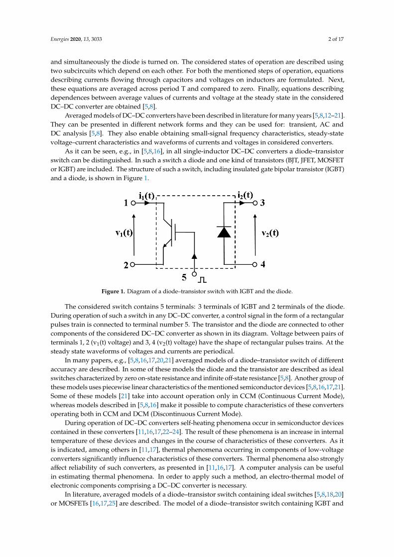
As it can be seen, e.g., in [5,8,16], in all single-inductor DC–DC converters a diode–transistorswitch can be distinguished. In such a switch a diode and one kind of transistors (BJT, JFET, MOSFETor IGBT) are included. The structure of such a switch, including insulated gate bipolar transistor (IGBT)and a diode, is shown in Figure 1.
Energies 2020, 13, x FOR PEER REVIEW 2 of 17
turned on, and simultaneously the diode is turned off. In the second step, the transistor is turned off
and simultaneously the diode is turned on. The considered states of operation are described using
two subcircuits which depend on each other. For both the mentioned steps of operation, equations
describing currents flowing through capacitors and voltages on inductors are formulated. Next, these
equations are averaged across period T and compared to zero. Finally, equations describing
dependences between average values of currents and voltage at the steady state in the considered
DC–DC converter are obtained [5,8].
Averaged models of DC–DC converters have been described in literature for many years [5,8,12–
21]. They can be presented in different network forms and they can be used for: transient, AC and
DC analysis [5,8]. They also enable obtaining small-signal frequency characteristics, steady-state
voltage–current characteristics and waveforms of currents and voltages in considered converters.
As it can be seen, e.g., in [5,8,16], in all single-inductor DC–DC converters a diode–transistor
switch can be distinguished. In such a switch a diode and one kind of transistors (BJT, JFET, MOSFET
or IGBT) are included. The structure of such a switch, including insulated gate bipolar transistor (IGBT)
and a diode, is shown in Figure 1.
Figure 1. Diagram of a diode–transistor switch with IGBT and the diode.
The considered switch contains 5 terminals: 3 terminals of IGBT and 2 terminals of the diode.
During operation of such a switch in any DC–DC converter, a control signal in the form of a
rectangular pulses train is connected to terminal number 5. The transistor and the diode are
connected to other components of the considered DC–DC converter as shown in its diagram. Voltage
between pairs of terminals 1, 2 (v1(t) voltage) and 3, 4 (v2(t) voltage) have the shape of rectangular
pulses trains. At the steady state waveforms of voltages and currents are periodical.
In many papers, e.g., [5,8,16,17,20,21] averaged models of a diode–transistor switch of different
accuracy are described. In some of these models the diode and the transistor are described as ideal
switches characterized by zero on-state resistance and infinite off-state resistance [5,8]. Another
group of these models uses piecewise linear characteristics of the mentioned semiconductor devices
[5,8,16,17,21]. Some of these models [21] take into account operation only in CCM (Continuous
Current Mode), whereas models described in [5,8,16] make it possible to compute characteristics of
these converters operating both in CCM and DCM (Discontinuous Current Mode).
During operation of DC–DC converters self-heating phenomena occur in semiconductor devices
contained in these converters [11,16,17,22–24]. The result of these phenomena is an increase in
internal temperature of these devices and changes in the course of characteristics of these converters.
As it is indicated, among others in [11,17], thermal phenomena occurring in components of low-
voltage converters significantly influence characteristics of these converters. Thermal phenomena
also strongly affect reliability of such converters, as presented in [11,16,17]. A computer analysis can
be useful in estimating thermal phenomena. In order to apply such a method, an electro-thermal
model of electronic components comprising a DC–DC converter is necessary.
In literature, averaged models of a diode–transistor switch containing ideal switches [5,8,18,20]
or MOSFETs [16,17,25] are described. The model of a diode–transistor switch containing IGBT and a
Figure 1. Diagram of a diode–transistor switch with IGBT and the diode.
The considered switch contains 5 terminals: 3 terminals of IGBT and 2 terminals of the diode.During operation of such a switch in any DC–DC converter, a control signal in the form of a rectangularpulses train is connected to terminal number 5. The transistor and the diode are connected to othercomponents of the considered DC–DC converter as shown in its diagram. Voltage between pairs ofterminals 1, 2 (v1(t) voltage) and 3, 4 (v2(t) voltage) have the shape of rectangular pulses trains. At thesteady state waveforms of voltages and currents are periodical.
In many papers, e.g., [5,8,16,17,20,21] averaged models of a diode–transistor switch of differentaccuracy are described. In some of these models the diode and the transistor are described as idealswitches characterized by zero on-state resistance and infinite off-state resistance [5,8]. Another group ofthese models uses piecewise linear characteristics of the mentioned semiconductor devices [5,8,16,17,21].Some of these models [21] take into account operation only in CCM (Continuous Current Mode),whereas models described in [5,8,16] make it possible to compute characteristics of these convertersoperating both in CCM and DCM (Discontinuous Current Mode).
During operation of DC–DC converters self-heating phenomena occur in semiconductor devicescontained in these converters [11,16,17,22–24]. The result of these phenomena is an increase in internaltemperature of these devices and changes in the course of characteristics of these converters. As itis indicated, among others in [11,17], thermal phenomena occurring in components of low-voltageconverters significantly influence characteristics of these converters. Thermal phenomena also stronglyaffect reliability of such converters, as presented in [11,16,17]. A computer analysis can be usefulin estimating thermal phenomena. In order to apply such a method, an electro-thermal model ofelectronic components comprising a DC–DC converter is necessary.
In literature, averaged models of a diode–transistor switch containing ideal switches [5,8,18,20]or MOSFETs [16,17,25] are described. The model of a diode–transistor switch containing IGBT and

Energies 2020, 13, 3033 3 of 17
a diode presented in the study [21] has a significantly simplified form. In the considered model,characteristics of the diode and IGBT are modeled using piecewise linear functions consisting of onlytwo pieces. Such a manner of modeling DC characteristics of IGBT and a diode can cause a significanterror of computations, especially in the range of low currents. Moreover, this model was verified onlyin the CCM. As it is pointed out in many papers [5,8,16], omitting DCM can also constitute a cause ofa significant error in computations. Finally, in the model presented in [21] thermal phenomena arenot taken into account. The electrothermal averaged model of a diode–transistor switch includingthe power MOS transistor is described in [16,17]. Such models enable computations of voltages andcurrents in the considered converter and internal temperatures of semiconductor devices contained inthe diode–transistor switch. Due to different shapes of output characteristics of IGBT and MOSFEToperating in the on–state, the cited models are not adequate to analyze characteristics of DC–DCconverters including IGBT and a diode.
In this study, the electrothermal averaged model of a diode–transistor switch including the IGBT isproposed. It is dedicated to electrothermal analysis of DC–DC converters containing such a switch andit makes it possible to compute values of current, voltage and internal temperatures of semiconductordevices contained in the mentioned switch. In electrothermal analyses, both electrical phenomenaoccurring in the analyzed DC–DC converter as well as self-heating phenomena occurring in bothsemiconductor devices are taken into account. In Section 2, the form of the elaborated model ispresented. In Section 3, a manner of estimating model parameters is described and some results ofmodeling DC characteristics of components of the diode–transistor switch are shown. In Section 4,the results of usefulness of the elaborated model for determining characteristics of the boost converterare presented and discussed.
2. Proposed Model
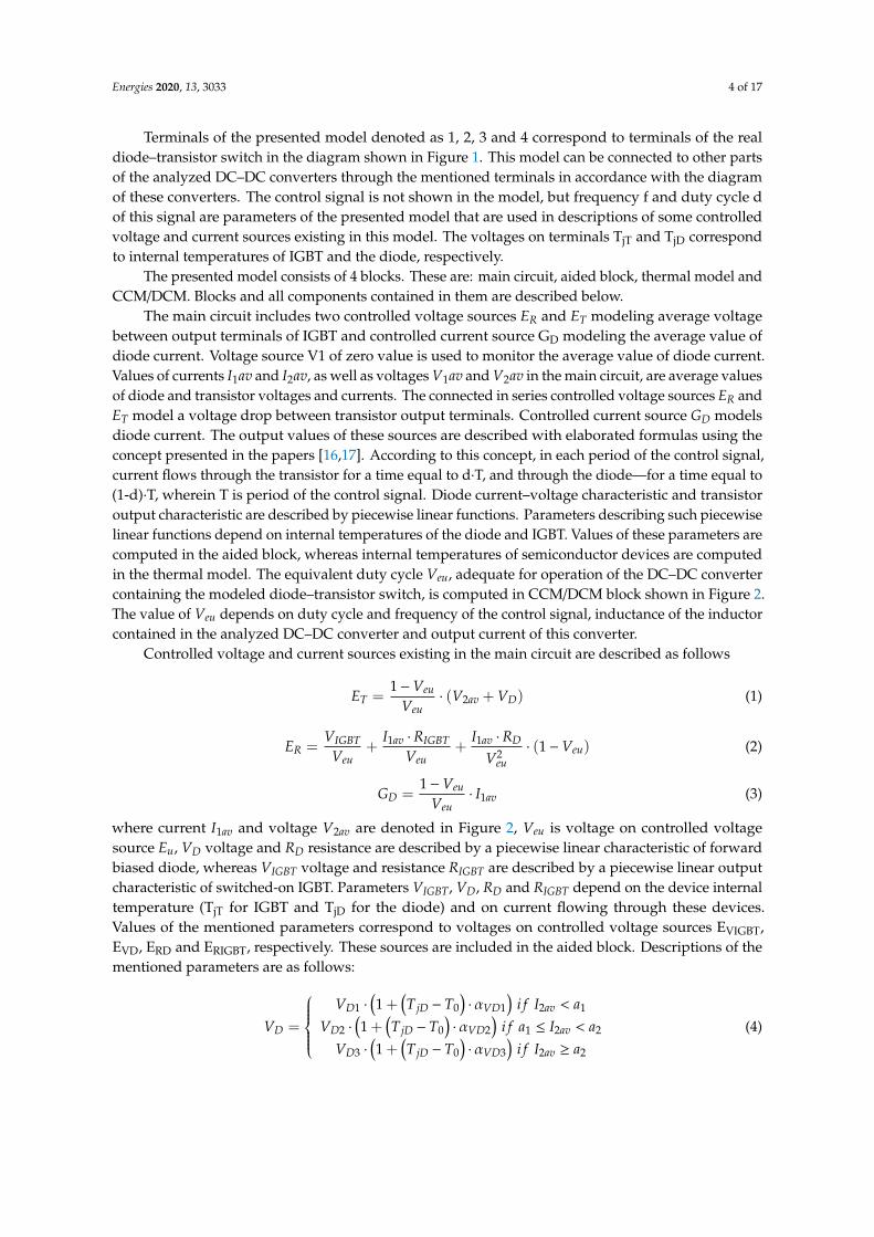
The formulated electrothermal model of a diode–transistor switch is based on the conceptdescribed in the study [16,17] for such a switch including the power MOS transistor. The networkrepresentation of the proposed electrothermal model of a diode–transistor switch (DTS) with IGBT anda diode is shown in Figure 2.
Energies 2020, 13, x FOR PEER REVIEW 3 of 17
diode presented in the study [21] has a significantly simplified form. In the considered model,
characteristics of the diode and IGBT are modeled using piecewise linear functions consisting of only
two pieces. Such a manner of modeling DC characteristics of IGBT and a diode can cause a significant
error of computations, especially in the range of low currents. Moreover, this model was verified only
in the CCM. As it is pointed out in many papers [5,8,16], omitting DCM can also constitute a cause of
a significant error in computations. Finally, in the model presented in [21] thermal phenomena are
not taken into account. The electrothermal averaged model of a diode–transistor switch including the
power MOS transistor is described in [16,17]. Such models enable computations of voltages and
currents in the considered converter and internal temperatures of semiconductor devices contained
in the diode–transistor switch. Due to different shapes of output characteristics of IGBT and MOSFET
operating in the on–state, the cited models are not adequate to analyze characteristics of DC–DC
converters including IGBT and a diode.
In this study, the electrothermal averaged model of a diode–transistor switch including the IGBT
is proposed. It is dedicated to electrothermal analysis of DC–DC converters containing such a switch
and it makes it possible to compute values of current, voltage and internal temperatures of
semiconductor devices contained in the mentioned switch. In electrothermal analyses, both electrical
phenomena occurring in the analyzed DC–DC converter as well as self-heating phenomena occurring
in both semiconductor devices are taken into account. In Section 2, the form of the elaborated model
is presented. In Section 3, a manner of estimating model parameters is described and some results of
modeling DC characteristics of components of the diode–transistor switch are shown. In Section 4,
the results of usefulness of the elaborated model for determining characteristics of the boost converter
are presented and discussed.
2. Proposed Model
The formulated electrothermal model of a diode–transistor switch is based on the concept
described in the study [16,17] for such a switch including the power MOS transistor. The network
representation of the proposed electrothermal model of a diode–transistor switch (DTS) with IGBT
and a diode is shown in Figure 2.
1
4
3
2
+
-
+
-
I1av I2av
V1av
GDET
Ga Ra
VaER V1
Eu
ERIGBTEVIGBT
EVDGTT GTD
Main
circuit
Thermal modelAided block
CCM/DCM
V2av
TjD
TjT
+-
+-
+-
+-
+-
+-
+- + -
Ex
+-
ERD
+-
+- VTa
RthT RthD
Veu Vx
RIGBT VIGBT VD RD
Figure 2. Network representation of the electrothermal averaged model of a diode–transistor switch
(DTS) including IGBT and a diode.
Figure 2. Network representation of the electrothermal averaged model of a diode–transistor switch(DTS) including IGBT and a diode.
Energies 2020, 13, 3033 4 of 17
Terminals of the presented model denoted as 1, 2, 3 and 4 correspond to terminals of the realdiode–transistor switch in the diagram shown in Figure 1. This model can be connected to other partsof the analyzed DC–DC converters through the mentioned terminals in accordance with the diagramof these converters. The control signal is not shown in the model, but frequency f and duty cycle dof this signal are parameters of the presented model that are used in descriptions of some controlledvoltage and current sources existing in this model. The voltages on terminals TjT and TjD correspondto internal temperatures of IGBT and the diode, respectively.
The presented model consists of 4 blocks. These are: main circuit, aided block, thermal model andCCM/DCM. Blocks and all components contained in them are described below.
The main circuit includes two controlled voltage sources ER and ET modeling average voltagebetween output terminals of IGBT and controlled current source GD modeling the average value ofdiode current. Voltage source V1 of zero value is used to monitor the average value of diode current.Values of currents I1av and I2av, as well as voltages V1av and V2av in the main circuit, are average valuesof diode and transistor voltages and currents. The connected in series controlled voltage sources ER andET model a voltage drop between transistor output terminals. Controlled current source GD modelsdiode current. The output values of these sources are described with elaborated formulas using theconcept presented in the papers [16,17]. According to this concept, in each period of the control signal,current flows through the transistor for a time equal to d·T, and through the diode—for a time equal to(1-d)·T, wherein T is period of the control signal. Diode current–voltage characteristic and transistoroutput characteristic are described by piecewise linear functions. Parameters describing such piecewiselinear functions depend on internal temperatures of the diode and IGBT. Values of these parameters arecomputed in the aided block, whereas internal temperatures of semiconductor devices are computedin the thermal model. The equivalent duty cycle Veu, adequate for operation of the DC–DC convertercontaining the modeled diode–transistor switch, is computed in CCM/DCM block shown in Figure 2.The value of Veu depends on duty cycle and frequency of the control signal, inductance of the inductorcontained in the analyzed DC–DC converter and output current of this converter.
Controlled voltage and current sources existing in the main circuit are described as follows
ET =1−Veu
Veu· (V2av + VD) (1)
ER =VIGBT
Veu+
I1av ·RIGBTVeu
+I1av ·RD
V2eu
· (1−Veu) (2)
GD =1−Veu
Veu· I1av (3)
where current I1av and voltage V2av are denoted in Figure 2, Veu is voltage on controlled voltagesource Eu, VD voltage and RD resistance are described by a piecewise linear characteristic of forwardbiased diode, whereas VIGBT voltage and resistance RIGBT are described by a piecewise linear outputcharacteristic of switched-on IGBT. Parameters VIGBT, VD, RD and RIGBT depend on the device internaltemperature (TjT for IGBT and TjD for the diode) and on current flowing through these devices.Values of the mentioned parameters correspond to voltages on controlled voltage sources EVIGBT,EVD, ERD and ERIGBT, respectively. These sources are included in the aided block. Descriptions of thementioned parameters are as follows:
VD =
VD1 ·
(1 +
(T jD − T0
)· αVD1
)i f I2av < a1
VD2 ·(1 +
(T jD − T0
)· αVD2
)i f a1 ≤ I2av < a2
VD3 ·(1 +
(T jD − T0
)· αVD3
)i f I2av ≥ a2
(4)

Energies 2020, 13, 3033 5 of 17
RD =
RD1 ·
(1 +
(T jD − T0
)· αRD1
)i f I2av < a1
RD2 ·(1 +
(T jD − T0
)· αRD2
)i f a1 ≤ I2av < a2
RD3 ·(1 +
(T jD − T0
)· αRD3
)i f I2av ≥ a2
(5)
VIGBT =
VIGBT1 ·
(1 +
(T jT − T0
)· αVIGBT1
)i f I1av < b1
VIGBT2 ·(1 +
(T jT − T0
)· αVIGBT2
)i f b1 ≤ I1av < b2
VIGBT3 ·(1 +
(T jT − T0
)· αVIGBT3
)i f I1av ≥ b2
(6)
RIGBT =
RIGBT1 ·
(1 +
(T jT − T0
)· αRIGBT1
)i f I1av < b1
RIGBT2 ·(1 +
(T jT − T0
)· αRIGBT2
)i f b1 ≤ I1av < b2
RIGBT3 ·(1 +
(T jT − T0
)· αRIGBT3
)i f I1av ≥ b2
(7)
In Equations (5) and (6) symbols VD1, VD2, VD3, RD1, RD2, RD3, αVD1, αVD2, αVD3, αRD1, αRD2,αRD3, a1 and a2 denote parameters of a piecewise linear model of diode DC characteristic. In turn,in Equations (6) and (7) symbols VIGBT1, VIGBT2, VIGBT3, RIGBT1, RIGBT2, RIGBT3, αVIGBT1, αVIGBT2,αVIGBT3, αRIGBT1, αRIGBT2, αRIGBT3, b1 and b2 denote parameters of a piecewise linear model of IGBToutput characteristics. Values of temperatures TjD and TjT are computed in the thermal model,whereas T0 represents reference temperature.
In the thermal model values of internal temperature of IGBT (TjT) and the diode (TjD) are computedwith self-heating phenomena taken into account. The classical electrical analog of a DC compactthermal model described, e.g., in [11,16,17,22,26,27] is used. In this analog temperature corresponds tovoltage in selected nodes of this analog, whereas dissipated power is represented by current sources.The ability to remove heat generated in the diode and in IGBT is characterized by thermal resistance.In the proposed model voltage source VTa represents ambient temperature, resistors RthT and RthDdenote thermal resistance of IGBT and the diode, respectively. Average values of power dissipatedin the considered semiconductor devices are represented by controlled current sources GTT and GTD.Currents flowing through these sources are described by the following formulas
GTD =(VD +
RD · I2av
1−Veu
)·
I2av
1−Veu(8)
GTT =(VIGBT +
RIGBT · I1avVeu
)·
I1avVeu
(9)
The proposed model can be used for computations of characteristics of DC–DC convertersoperating in CCM or DCM. In both mentioned modes of operation in each period of a control signalthe transistor is turned on in time equal to the product of duty cycle d and period T. In turn, the diodeis turned on in time equal to (1-d)·T in CCM and this time is shorter in DCM. In order to take intoaccount influence of duty cycle d, frequency f of the control signal and inductance L of the inductorincluded in the tested DC–DC converter on voltage Veu, CCM/DCM block is included in the model.This block includes controlled current source Ga, voltage source Va of zero value, resistor Ra andcontrolled voltage sources Eu and Ex.
Voltage Veu on voltage source Eu is described by the formula
Veu =
0 i f Vx < 0
Vx i f 0 < Vx
1 i f Vx > 1< 1 (10)
where voltage Vx on voltage source Ex is described as follows
Vx = LIMIT
MAX
d,d2
d2 + 2 · L · f · IVaV2av+VD
, 0, 1
(11)

Energies 2020, 13, 3033 6 of 17
In Equation (11) LIMIT (·) and MAX (·) are SPICE standard functions described, e.g., in thebook [28] and IVa denotes current flowing through controlled current source Ga described with theformula of the form:
Ga = MAX(I1av, 0) (12)
Resistor Ra must be included in this block due to formal rules of SPICE. Voltage source Va is usedto monitor the value of current IVa.
3. Estimation of Model Parameters
Practical applications of the proposed model require estimation of parameter values existingin this model. For example, an estimate is performed for the IGBT of the type IGP06N60T [29] byInfineon Technologies and for the diode of the type IDP08E65 [30] by Infineon Technologies. Input dataare characteristics of such devices measured by the authors with the use of the impulse method [31]and a source-meter Keithley 2612a [32] at different fixed values of ambient temperature. When thesemeasurements are performed, the tested semiconductor devices are situated in a thermal chamber,in which the adjustable value of temperature can be obtained.
Values of the model parameters obtained by matching piecewise linear models of characteristicsof the considered devices are given in Table 1.
Table 1. Values of parameters of the piecewise linear model of the used insulated gate bipolar transistor(IGBT) and diode.
Parameter Name VD1 (V) VD2 (V) VD3 (V) αVD1 (K-1) αVD2 (K-1) αVD3 (K-1) a1 (A)Parameter Value 0.63 0.74 0.847 −8.41 × 10⁻³
−3.92 × 10⁻³−2.95 × 10⁻³ 0.25
Parameter Name RD1 (Ω) RD2 (Ω) RD3 (Ω) αRD1 (K−1) αRD2 (K−1) αRD3 (K−1) a2 (A)Parameter Value 0.75 0.191 0.1 4.67 × 10⁻³ 2.62 × 10⁻³ 1.74 × 10⁻³ 1.3
Parameter Name VIGBT1 (V) VIGBT2 (V) VIGBT3 (V) αVIGBT1 (K−1) αVIGBT2 (K−1) αVIGBT3 (K−1) b1 (A)Parameter Value 0.611 0.736 0.811 −3.04 × 10⁻³
−1.63 × 10⁻³−1.2 × 10⁻³ 0.52
Parameter Name RIGBT1 (Ω) RIGBT2 (Ω) RIGBT3 (Ω) αRIGBT1 (K−1) αRIGBT2 (K−1) αRIGBT3 (K−1) b2 (A)Parameter Value 0.443 0.195 0.127 3.61 × 10⁻³ 2.05 × 10⁻³ 1.9 × 10⁻³ 1.2
In Figures 3 and 4 measured (points) and computed (lines) characteristics of the diode (Figure 3)and IGBT (Figure 4) are shown. These characteristics are measured and computed at selected values ofambient temperature Ta.Energies 2020, 13, x FOR PEER REVIEW 7 of 17
Figure 3. Characteristics of a forward-biased diode computed with the use of a piecewise linear model
(lines) and measured (points) at selected values of temperature Ta.
Figure 4. Output characteristics of insulated gate bipolar transistor (IGBT) computed with the use of
a piecewise linear model (lines) and measured (points) at selected values of temperature Ta.
The presented characteristics correspond to isothermal operating conditions of tested devices,
at which self-heating phenomena can be omitted. In the real case, device internal temperature is
higher than ambient temperature as a result of the mentioned phenomena [26,27,33]. The cooling
conditions of this device are characterized by thermal resistance. This parameter is measured using
impulse electrical methods described in [34–36].
Both considered semiconductor devices are situated in the TO-220 case. The measured values of
IGBT and the diode are nearly the same and they are equal to about 44 K/W. Reference temperature
T0 is equal to 20 °C.
4. Results of Measurements and Computations
In order to verify usefulness of the proposed electrothermal averaged model of a diode–
transistor switch, measurements and computations of characteristics of the boost converter with
considered semiconductor devices were performed. A diagram of the tested converter is shown in
Figure 5, whereas a photo of the tested converter is presented in Figure 6.
0
0.5
1
1.5
2
2.5
3
0 0.2 0.4 0.6 0.8 1 1.2
I D [
A]
VD [V]
Ta = 20oC
Ta = 120oC
0
0.5
1
1.5
2
2.5
3
3.5
4
4.5
5
0 0.1 0.2 0.3 0.4 0.5 0.6 0.7 0.8 0.9 1 1.1 1.2 1.3 1.4 1.5
I C [
A]
VCE [V]
Ta = 20oC
Ta = 122oC
Figure 3. Characteristics of a forward-biased diode computed with the use of a piecewise linear model(lines) and measured (points) at selected values of temperature Ta.

Energies 2020, 13, 3033 7 of 17
Energies 2020, 13, x FOR PEER REVIEW 7 of 17
Figure 3. Characteristics of a forward-biased diode computed with the use of a piecewise linear model
(lines) and measured (points) at selected values of temperature Ta.
Figure 4. Output characteristics of insulated gate bipolar transistor (IGBT) computed with the use of
a piecewise linear model (lines) and measured (points) at selected values of temperature Ta.
The presented characteristics correspond to isothermal operating conditions of tested devices,
at which self-heating phenomena can be omitted. In the real case, device internal temperature is
higher than ambient temperature as a result of the mentioned phenomena [26,27,33]. The cooling
conditions of this device are characterized by thermal resistance. This parameter is measured using
impulse electrical methods described in [34–36].
Both considered semiconductor devices are situated in the TO-220 case. The measured values of
IGBT and the diode are nearly the same and they are equal to about 44 K/W. Reference temperature
T0 is equal to 20 °C.
4. Results of Measurements and Computations
In order to verify usefulness of the proposed electrothermal averaged model of a diode–
transistor switch, measurements and computations of characteristics of the boost converter with
considered semiconductor devices were performed. A diagram of the tested converter is shown in
Figure 5, whereas a photo of the tested converter is presented in Figure 6.
0
0.5
1
1.5
2
2.5
3
0 0.2 0.4 0.6 0.8 1 1.2
I D [
A]
VD [V]
Ta = 20oC
Ta = 120oC
0
0.5
1
1.5
2
2.5
3
3.5
4
4.5
5
0 0.1 0.2 0.3 0.4 0.5 0.6 0.7 0.8 0.9 1 1.1 1.2 1.3 1.4 1.5
I C [
A]
VCE [V]
Ta = 20oC
Ta = 122oC
Figure 4. Output characteristics of insulated gate bipolar transistor (IGBT) computed with the use of apiecewise linear model (lines) and measured (points) at selected values of temperature Ta.
As is visible, the results of measurements and computations are convergent for both consideredsemiconductor devices in a wide range of changes of ambient temperature Ta. As can be observed,all characteristics are described using 4 line segments. A slope of the considered characteristics increaseswith an increase of the main current of the tested device. This means that series resistances of the diodeand IGBT decrease with an increase of this current. It is also observed that the diode forward-voltageand on-voltage of IGBT at zero current decreases with an increase in ambient temperature.
With the diode, an increase in temperature causes a decrease in diode forward-voltage. In turn,for IGBT with a range of low collector current values, an increase in ambient temperature causes adecrease in on–voltage of IGBT. In contrast, for high collector current values, an increase in temperatureTa causes an increase in on–voltage of IGBT.
The presented characteristics correspond to isothermal operating conditions of tested devices,at which self-heating phenomena can be omitted. In the real case, device internal temperature is higherthan ambient temperature as a result of the mentioned phenomena [26,27,33]. The cooling conditionsof this device are characterized by thermal resistance. This parameter is measured using impulseelectrical methods described in [34–36].
Both considered semiconductor devices are situated in the TO-220 case. The measured values ofIGBT and the diode are nearly the same and they are equal to about 44 K/W. Reference temperature T0
is equal to 20 C.
4. Results of Measurements and Computations
In order to verify usefulness of the proposed electrothermal averaged model of a diode–transistorswitch, measurements and computations of characteristics of the boost converter with consideredsemiconductor devices were performed. A diagram of the tested converter is shown in Figure 5,whereas a photo of the tested converter is presented in Figure 6.
In the considered converter, the input voltage Vin was equal to 12 V, and R0 was load resistance.The inductance of inductor L1 was equal to 560 µH and capacitance of capacitor C1 was equal to 1 mF.Voltage source Vctrl produced a rectangular pulsed train of frequency f equal to 10 kHz and duty cycled. Ammeters were used to measure the input and output currents of the tested converter. Internalresistance of these ammeters was equal to 0.31 Ω. The prototype was mounted on a PCB; the diode ofthe type IDP08E65 and IGBT of the type IGP06N60T operated without any heat-sinks. The controlsignal was given by a signal generator exciting gate driver IR2125 by Infineon Technologies.
Some waveforms of voltages and currents of the tested DC–DC converter were measured usingan oscilloscope Rigol MS05104 and current probe Tektronix PCPA 300 for different parameters ofthe control signal and load resistances. For example, in Figure 7 measured waveforms of vGE(t)

Energies 2020, 13, 3033 8 of 17
voltage (yellow line), vCE(t) voltage (violet line) and iL(t) current (blue line) are shown. The mentionedquantities are marked in Figure 5. Waveform of iL(t) was obtained after conversion of the measuredcurrent into voltage in the current probe. The conversion coefficient was equal to 1 A/V. During thesemeasurements load resistance R0 was equal to 47 Ω.Energies 2020, 13, x FOR PEER REVIEW 8 of 17
D1
C1
R0
L1
RG
Vin
Vout
Vctrl
T1
A A
vCE
vGE
iL iout
Figure 5. Diagram of the tested boost converter.
Figure 6. Photo of the tested boost converter.
In the considered converter, the input voltage Vin was equal to 12 V, and R0 was load resistance.
The inductance of inductor L1 was equal to 560 µH and capacitance of capacitor C1 was equal to 1
mF. Voltage source Vctrl produced a rectangular pulsed train of frequency f equal to 10 kHz and duty
cycle d. Ammeters were used to measure the input and output currents of the tested converter.
Internal resistance of these ammeters was equal to 0.31 Ω. The prototype was mounted on a PCB; the
diode of the type IDP08E65 and IGBT of the type IGP06N60T operated without any heat-sinks. The
control signal was given by a signal generator exciting gate driver IR2125 by Infineon Technologies.
Some waveforms of voltages and currents of the tested DC–DC converter were measured using
an oscilloscope Rigol MS05104 and current probe Tektronix PCPA 300 for different parameters of the
control signal and load resistances. For example, in Figure 7 measured waveforms of vGE(t) voltage
(yellow line), vCE(t) voltage (violet line) and iL(t) current (blue line) are shown. The mentioned
quantities are marked in Figure 5. Waveform of iL(t) was obtained after conversion of the measured
current into voltage in the current probe. The conversion coefficient was equal to 1 A/V. During these
measurements load resistance R0 was equal to 47 Ω.
As it can be observed, the signal controlling the input of IGBT (vGE voltage) had frequency equal
to 10 kHz, duty cycle equal to 0.5, low level voltage equal to zero and high level voltage equal to 15
V. These parameters values of the control signal were adequate for the used transistor. The transistor
output voltage vCE(t) had a shape of a rectangular pulsed train. The highest level of this voltage was
equal to about 22 V. The current iL(t) had positive values only, which proved that the tested converter
operated in CCM.
Figure 5. Diagram of the tested boost converter.
Energies 2020, 13, x FOR PEER REVIEW 8 of 17
D1
C1
R0
L1
RG
Vin
Vout
Vctrl
T1
A A
vCE
vGE
iL iout
Figure 5. Diagram of the tested boost converter.
Figure 6. Photo of the tested boost converter.
In the considered converter, the input voltage Vin was equal to 12 V, and R0 was load resistance.
The inductance of inductor L1 was equal to 560 µH and capacitance of capacitor C1 was equal to 1
mF. Voltage source Vctrl produced a rectangular pulsed train of frequency f equal to 10 kHz and duty
cycle d. Ammeters were used to measure the input and output currents of the tested converter.
Internal resistance of these ammeters was equal to 0.31 Ω. The prototype was mounted on a PCB; the
diode of the type IDP08E65 and IGBT of the type IGP06N60T operated without any heat-sinks. The
control signal was given by a signal generator exciting gate driver IR2125 by Infineon Technologies.
Some waveforms of voltages and currents of the tested DC–DC converter were measured using
an oscilloscope Rigol MS05104 and current probe Tektronix PCPA 300 for different parameters of the
control signal and load resistances. For example, in Figure 7 measured waveforms of vGE(t) voltage
(yellow line), vCE(t) voltage (violet line) and iL(t) current (blue line) are shown. The mentioned
quantities are marked in Figure 5. Waveform of iL(t) was obtained after conversion of the measured
current into voltage in the current probe. The conversion coefficient was equal to 1 A/V. During these
measurements load resistance R0 was equal to 47 Ω.
As it can be observed, the signal controlling the input of IGBT (vGE voltage) had frequency equal
to 10 kHz, duty cycle equal to 0.5, low level voltage equal to zero and high level voltage equal to 15
V. These parameters values of the control signal were adequate for the used transistor. The transistor
output voltage vCE(t) had a shape of a rectangular pulsed train. The highest level of this voltage was
equal to about 22 V. The current iL(t) had positive values only, which proved that the tested converter
operated in CCM.
Figure 6. Photo of the tested boost converter.Energies 2020, 13, x FOR PEER REVIEW 9 of 17
Figure 7. Measured waveforms of vGE(t) voltage, vCE(t) voltages and iL(t) current in the tested boost
converter operating at load resistance R0 = 47 Ω
It is important to notice that the tested DC–DC converter operated without any feedback loop,
typically used in switch-mode power supplies including such converters. At the chosen operating
condition, the influence of parameters of the control signal and on the load resistance were not
compensated by the feedback loop. Therefore, any disadvantages of the proposed model can be
clearly illustrated for the tested circuit.
Selected resulted of measurements and computations of the considered DC–DC converter are
shown in the successive figures. In these figures points denote the results of measurements, solid
lines—the results of computations performed with the use of the proposed electrothermal averaged
model of a diode–transistor switch including IGBT and a rapid switching diode (called also the new
model), black dashed lines—the results of computations performed with the use of the averaged
model of a diode transistor switch with ideal switches described e.g., in [5,8] and blue dotted lines—
the results of computations performed with the use of the averaged model of a diode–transistor
switch including IGBT described in [21].
Figures 8–11 present computed and measured characteristics of the considered converter
operating at the fixed value of duty cycle d = 0.5 and the varied value of load resistance R0. In turn,
Figures 12–15 show characteristics of this converter operating at the fixed value of load resistance R0
= 47 Ω and the varied value of duty cycle d. Values of voltages and currents were measured with the
used of laboratory voltmeters and ammeters. The diode and transistor temperatures were measured
with the use of an infrared method performed with a pyrometer PT-3S by Optex [37]. This instrument
made it possible to measure the case temperature of the mentioned semiconductor devices. Due to a
very small value of junction–case thermal resistance of the considered semiconductor devices—
which was much lower than junction-ambient thermal resistance—a difference between internal and
case temperatures of these devices was not higher than 5 °C.
Figure 8. Computed and measured dependences of boost converter output voltage on load resistance.
0
20
40
60
80
100
120
140
0.01 0.1 1 10
Vo
ut[V
]
R0 [kW]
Vin = 12 V
Ta = 20oC
d = 0.5
model from [5, 8]
model from [21]
new model
CCM
DCM
Figure 7. Measured waveforms of vGE(t) voltage, vCE(t) voltages and iL(t) current in the tested boostconverter operating at load resistance R0 = 47 Ω.

Energies 2020, 13, 3033 9 of 17
As it can be observed, the signal controlling the input of IGBT (vGE voltage) had frequency equalto 10 kHz, duty cycle equal to 0.5, low level voltage equal to zero and high level voltage equal to 15 V.These parameters values of the control signal were adequate for the used transistor. The transistoroutput voltage vCE(t) had a shape of a rectangular pulsed train. The highest level of this voltage wasequal to about 22 V. The current iL(t) had positive values only, which proved that the tested converteroperated in CCM.
It is important to notice that the tested DC–DC converter operated without any feedback loop,typically used in switch-mode power supplies including such converters. At the chosen operatingcondition, the influence of parameters of the control signal and on the load resistance were notcompensated by the feedback loop. Therefore, any disadvantages of the proposed model can be clearlyillustrated for the tested circuit.
Selected resulted of measurements and computations of the considered DC–DC converterare shown in the successive figures. In these figures points denote the results of measurements,solid lines—the results of computations performed with the use of the proposed electrothermalaveraged model of a diode–transistor switch including IGBT and a rapid switching diode (calledalso the new model), black dashed lines—the results of computations performed with the use of theaveraged model of a diode transistor switch with ideal switches described e.g., in [5,8] and blue dottedlines—the results of computations performed with the use of the averaged model of a diode–transistorswitch including IGBT described in [21].
Figures 8–11 present computed and measured characteristics of the considered converter operatingat the fixed value of duty cycle d = 0.5 and the varied value of load resistance R0. In turn, Figures 12–15show characteristics of this converter operating at the fixed value of load resistance R0 = 47 Ω andthe varied value of duty cycle d. Values of voltages and currents were measured with the used oflaboratory voltmeters and ammeters. The diode and transistor temperatures were measured with theuse of an infrared method performed with a pyrometer PT-3S by Optex [37]. This instrument made itpossible to measure the case temperature of the mentioned semiconductor devices. Due to a very smallvalue of junction–case thermal resistance of the considered semiconductor devices—which was muchlower than junction-ambient thermal resistance—a difference between internal and case temperaturesof these devices was not higher than 5 C.
In Figure 8 measured and computed dependences of converter output voltage Vout on loadresistance R0 are presented. As is visible, in the considered operating conditions, the boost converteroperated in CCM for R0 < 100 Ω and in DCM for R0 > 100 Ω. In both modes of operation, the newmodel guarantees good accuracy of computations. At small values of load resistance, a decreasewas visible in the value of output voltage caused by influence of a voltage drop on the switched ontransistor and diode. This voltage drop was an increasing function of converter output current and adecreasing function of load resistance R0. Literature models described in [5,8,21] could be used for theconverter operating in CCM only, because differences between the results of computations performedwith these models and the results of measurements were acceptable only in this mode. Of course,the results performed with the use of the model proposed in [21] were more convergent with the resultsof measurements in CCM than the results performed with the model given in [5,8].
Figure 9 presents dependences of watt-hour efficiency of the considered DC–DC converter onload resistance.
The obtained values of watt-hour efficiency were in the range from 0.8 to 0.9. Values of thisparameter computed using the electrothermal model differed from the results of measurements by nomore than 7%. The resulted obtained using the considered literature models were overstated even by17%.
In Figure 10 dependence of internal temperature of IGBT on load resistance was shown.Such dependence could be obtained with the use of the electrothermal model only.

Energies 2020, 13, 3033 10 of 17
Energies 2020, 13, x FOR PEER REVIEW 9 of 17
Figure 7. Measured waveforms of vGE(t) voltage, vCE(t) voltages and iL(t) current in the tested boost
converter operating at load resistance R0 = 47 Ω
It is important to notice that the tested DC–DC converter operated without any feedback loop,
typically used in switch-mode power supplies including such converters. At the chosen operating
condition, the influence of parameters of the control signal and on the load resistance were not
compensated by the feedback loop. Therefore, any disadvantages of the proposed model can be
clearly illustrated for the tested circuit.
Selected resulted of measurements and computations of the considered DC–DC converter are
shown in the successive figures. In these figures points denote the results of measurements, solid
lines—the results of computations performed with the use of the proposed electrothermal averaged
model of a diode–transistor switch including IGBT and a rapid switching diode (called also the new
model), black dashed lines—the results of computations performed with the use of the averaged
model of a diode transistor switch with ideal switches described e.g., in [5,8] and blue dotted lines—
the results of computations performed with the use of the averaged model of a diode–transistor
switch including IGBT described in [21].
Figures 8–11 present computed and measured characteristics of the considered converter
operating at the fixed value of duty cycle d = 0.5 and the varied value of load resistance R0. In turn,
Figures 12–15 show characteristics of this converter operating at the fixed value of load resistance R0
= 47 Ω and the varied value of duty cycle d. Values of voltages and currents were measured with the
used of laboratory voltmeters and ammeters. The diode and transistor temperatures were measured
with the use of an infrared method performed with a pyrometer PT-3S by Optex [37]. This instrument
made it possible to measure the case temperature of the mentioned semiconductor devices. Due to a
very small value of junction–case thermal resistance of the considered semiconductor devices—
which was much lower than junction-ambient thermal resistance—a difference between internal and
case temperatures of these devices was not higher than 5 °C.
Figure 8. Computed and measured dependences of boost converter output voltage on load resistance.
0
20
40
60
80
100
120
140
0.01 0.1 1 10
Vo
ut[V
]
R0 [kW]
Vin = 12 V
Ta = 20oC
d = 0.5
model from [5, 8]
model from [21]
new model
CCM
DCM
Figure 8. Computed and measured dependences of boost converter output voltage on load resistance.Energies 2020, 13, x FOR PEER REVIEW 10 of 17
Figure 9. Computed and measured dependences of watt-hour efficiency of the boost converter on
load resistance.
Figure 10. Computed and measured dependence of internal temperature of IGBT on load resistance.
Figure 11. Computed and measured dependence of internal temperature of the diode on load
resistance.
0.6
0.65
0.7
0.75
0.8
0.85
0.9
0.95
1
1.05
0.01 0.1 1 10
h
R0 [kW]
Vin = 12 V
Ta = 20oC
d = 0.5
model from [5, 8]
model from [21]
new model
20
30
40
50
60
70
80
90
100
110
120
0.01 0.1 1 10
TjT
[oC
]
R0 [kW]
Vin = 12 V
Ta = 20oC
d = 0.5
20
30
40
50
60
70
80
90
100
110
120
0.01 0.1 1 10
TjD
[oC
]
R0 [kW]
Vin = 12 V
Ta = 20oC
d = 0.5
Figure 9. Computed and measured dependences of watt-hour efficiency of the boost converter onload resistance.
Energies 2020, 13, x FOR PEER REVIEW 10 of 17
Figure 9. Computed and measured dependences of watt-hour efficiency of the boost converter on
load resistance.
Figure 10. Computed and measured dependence of internal temperature of IGBT on load resistance.
Figure 11. Computed and measured dependence of internal temperature of the diode on load
resistance.
0.6
0.65
0.7
0.75
0.8
0.85
0.9
0.95
1
1.05
0.01 0.1 1 10
h
R0 [kW]
Vin = 12 V
Ta = 20oC
d = 0.5
model from [5, 8]
model from [21]
new model
20
30
40
50
60
70
80
90
100
110
120
0.01 0.1 1 10
TjT
[oC
]
R0 [kW]
Vin = 12 V
Ta = 20oC
d = 0.5
20
30
40
50
60
70
80
90
100
110
120
0.01 0.1 1 10
TjD
[oC
]
R0 [kW]
Vin = 12 V
Ta = 20oC
d = 0.5
Figure 10. Computed and measured dependence of internal temperature of IGBT on load resistance.

Energies 2020, 13, 3033 11 of 17
Energies 2020, 13, x FOR PEER REVIEW 10 of 17
Figure 9. Computed and measured dependences of watt-hour efficiency of the boost converter on
load resistance.
Figure 10. Computed and measured dependence of internal temperature of IGBT on load resistance.
Figure 11. Computed and measured dependence of internal temperature of the diode on load
resistance.
0.6
0.65
0.7
0.75
0.8
0.85
0.9
0.95
1
1.05
0.01 0.1 1 10
h
R0 [kW]
Vin = 12 V
Ta = 20oC
d = 0.5
model from [5, 8]
model from [21]
new model
20
30
40
50
60
70
80
90
100
110
120
0.01 0.1 1 10
TjT
[oC
]
R0 [kW]
Vin = 12 V
Ta = 20oC
d = 0.5
20
30
40
50
60
70
80
90
100
110
120
0.01 0.1 1 10
TjD
[oC
]
R0 [kW]
Vin = 12 V
Ta = 20oC
d = 0.5
Figure 11. Computed and measured dependence of internal temperature of the diode on load resistance.Energies 2020, 13, x FOR PEER REVIEW 11 of 17
Figure 12. Computed and measured dependences of boost converter output voltage on duty cycle.
Figure 13. Computed and measured dependences of watt-hour efficiency of boost converter on duty
cycle.
Figure 14. Computed and measured dependences of internal temperature of IGBT on duty cycle.
0
20
40
60
80
100
120
140
0 0.2 0.4 0.6 0.8 1
Vou
t[V
]
d
Vin = 12 V
Ta = 20oC
R0 = 47 W
model from [5, 8]
model
from [21]
new model
0
0.2
0.4
0.6
0.8
1
1.2
0 0.2 0.4 0.6 0.8 1
h
d
Vin = 12 V
Ta = 20oC
R0 = 47 W
new model
model from [5, 8]model from [21]
0
20
40
60
80
100
120
140
0 0.2 0.4 0.6 0.8 1
TjT
[oC
]
d
Vin = 12 V
Ta = 20oC
R0 = 47 W
Figure 12. Computed and measured dependences of boost converter output voltage on duty cycle.
Energies 2020, 13, x FOR PEER REVIEW 11 of 17
Figure 12. Computed and measured dependences of boost converter output voltage on duty cycle.
Figure 13. Computed and measured dependences of watt-hour efficiency of boost converter on duty
cycle.
Figure 14. Computed and measured dependences of internal temperature of IGBT on duty cycle.
0
20
40
60
80
100
120
140
0 0.2 0.4 0.6 0.8 1
Vou
t[V
]
d
Vin = 12 V
Ta = 20oC
R0 = 47 W
model from [5, 8]
model
from [21]
new model
0
0.2
0.4
0.6
0.8
1
1.2
0 0.2 0.4 0.6 0.8 1
h
d
Vin = 12 V
Ta = 20oC
R0 = 47 W
new model
model from [5, 8]model from [21]
0
20
40
60
80
100
120
140
0 0.2 0.4 0.6 0.8 1
TjT
[oC
]
d
Vin = 12 V
Ta = 20oC
R0 = 47 W
Figure 13. Computed and measured dependences of watt-hour efficiency of boost converter onduty cycle.

Energies 2020, 13, 3033 12 of 17
Energies 2020, 13, x FOR PEER REVIEW 11 of 17
Figure 12. Computed and measured dependences of boost converter output voltage on duty cycle.
Figure 13. Computed and measured dependences of watt-hour efficiency of boost converter on duty
cycle.
Figure 14. Computed and measured dependences of internal temperature of IGBT on duty cycle.
0
20
40
60
80
100
120
140
0 0.2 0.4 0.6 0.8 1
Vou
t[V
]
d
Vin = 12 V
Ta = 20oC
R0 = 47 W
model from [5, 8]
model
from [21]
new model
0
0.2
0.4
0.6
0.8
1
1.2
0 0.2 0.4 0.6 0.8 1
h
d
Vin = 12 V
Ta = 20oC
R0 = 47 W
new model
model from [5, 8]model from [21]
0
20
40
60
80
100
120
140
0 0.2 0.4 0.6 0.8 1
TjT
[oC
]
d
Vin = 12 V
Ta = 20oC
R0 = 47 W
Figure 14. Computed and measured dependences of internal temperature of IGBT on duty cycle.Energies 2020, 13, x FOR PEER REVIEW 12 of 17
Figure 15. Computed and measured dependences of internal temperature of the diode on duty cycle.
In Figure 8 measured and computed dependences of converter output voltage Vout on load
resistance R0 are presented. As is visible, in the considered operating conditions, the boost converter
operated in CCM for R0 < 100 Ω and in DCM for R0 > 100 Ω. In both modes of operation, the new
model guarantees good accuracy of computations. At small values of load resistance, a decrease was
visible in the value of output voltage caused by influence of a voltage drop on the switched on
transistor and diode. This voltage drop was an increasing function of converter output current and a
decreasing function of load resistance R0. Literature models described in [5,8,21] could be used for
the converter operating in CCM only, because differences between the results of computations
performed with these models and the results of measurements were acceptable only in this mode. Of
course, the results performed with the use of the model proposed in [21] were more convergent with
the results of measurements in CCM than the results performed with the model given in [5,8].
Figure 9 presents dependences of watt-hour efficiency of the considered DC–DC converter on
load resistance.
The obtained values of watt-hour efficiency were in the range from 0.8 to 0.9. Values of this
parameter computed using the electrothermal model differed from the results of measurements by
no more than 7%. The resulted obtained using the considered literature models were overstated even
by 17%.
In Figure 10 dependence of internal temperature of IGBT on load resistance was shown. Such
dependence could be obtained with the use of the electrothermal model only.
As can be seen, very good accuracy in modeling this dependence was obtained only was CCM.
In DCM differences between the results of measurements and computations increased with an
increase in load resistance. They exceeded even 20 °C at R0 > 6 kΩ which could be connected with a
long switching-off process of IGBT [38], that was not taken into account in the proposed model.
In Figure 11 measured and computed (using the new model) dependence of internal
temperature of diode on load resistance is shown.
The considered dependence is a monotonically decreasing function. The result of computations
were convergent with the results of measurements. Differences did not exceed 4 °C. Of course, the
considered literature models did not make it possible to compute such dependence.
Figure 12 shows computed (with the new model) and measured dependences of converter
output voltage on duty cycle.
In the whole considered range of changes of duty cycle the tested boost converter operated in
CCM. The measured dependence Vout(d) is a monotonically increasing function, but measurements
were performed only for d < 0.67. The range of changes of d was limited due to a high increase in
internal temperature of IGBT, which attained even 120 °C. The considered dependences computed
using the electrothermal model and the model given in [21] had maxima at d > 0.9. These maxima
were observed due to voltage drops on switched-on semiconductor devices [16]. It was also visible
0
20
40
60
80
100
120
140
0 0.2 0.4 0.6 0.8 1
TjD
[oC
]
d
Vin = 12 V
Ta = 20oC
R0 = 47 W
Figure 15. Computed and measured dependences of internal temperature of the diode on duty cycle.
As can be seen, very good accuracy in modeling this dependence was obtained only was CCM.In DCM differences between the results of measurements and computations increased with an increasein load resistance. They exceeded even 20 C at R0 > 6 kΩ which could be connected with a longswitching-off process of IGBT [38], that was not taken into account in the proposed model.
In Figure 11 measured and computed (using the new model) dependence of internal temperatureof diode on load resistance is shown.
The considered dependence is a monotonically decreasing function. The result of computationswere convergent with the results of measurements. Differences did not exceed 4 C. Of course,the considered literature models did not make it possible to compute such dependence.
Figure 12 shows computed (with the new model) and measured dependences of converter outputvoltage on duty cycle.
In the whole considered range of changes of duty cycle the tested boost converter operated inCCM. The measured dependence Vout(d) is a monotonically increasing function, but measurementswere performed only for d < 0.67. The range of changes of d was limited due to a high increase ininternal temperature of IGBT, which attained even 120 C. The considered dependences computedusing the electrothermal model and the model given in [21] had maxima at d > 0.9. These maximawere observed due to voltage drops on switched-on semiconductor devices [16]. It was also visiblethat due to self-heating the value of these maxima decrease even three times. Differences between theresults of measurements and computations were small and they do not exceed 5%.
Figure 13 illustrates dependence of watt-hour efficiency of the tested boost converter on duty cycle.

Energies 2020, 13, 3033 13 of 17
As can be observed, dependences η(d) were monotonically decreasing functions. The resultsof computations performed with the electrothermal model were convergent with the result ofmeasurements. Differences do not exceed 2%. Values of watt-hour efficiency computed usingthe other models were overstated even by 15%.
Figure 14 presents measured and computed (with the new model) dependence of internaltemperature of IGBT on duty cycle.
The considered dependence was an increasing function. The results of computations differ fromthe results of measurements not more than 5 C.
Figure 15 shows measured and computed (with the new model) dependence of internal temperatureof the diode on duty cycle.
It can be easily observed that temperature TjD increased with an increase in duty cycle. This meansthat the power dissipated in this diode increased, despite the fact that the time in which this diode wasforward-biased decreased. The differences between the results of computations and measurements didnot exceed a few degrees Celsius.
Figure 16 illustrates influence of duty-cycle on the output characteristics of the tested DC–DCconverter (Figure 16a) and the dependence of diode internal temperature on the converter’s outputcurrent iout.
Energies 2020, 13, x FOR PEER REVIEW 13 of 17
that due to self-heating the value of these maxima decrease even three times. Differences between the
results of measurements and computations were small and they do not exceed 5%.
Figure 13 illustrates dependence of watt-hour efficiency of the tested boost converter on duty
cycle.
As can be observed, dependences η(d) were monotonically decreasing functions. The results of
computations performed with the electrothermal model were convergent with the result of
measurements. Differences do not exceed 2%. Values of watt-hour efficiency computed using the
other models were overstated even by 15%.
Figure 14 presents measured and computed (with the new model) dependence of internal
temperature of IGBT on duty cycle.
The considered dependence was an increasing function. The results of computations differ from
the results of measurements not more than 5 °C.
Figure 15 shows measured and computed (with the new model) dependence of internal
temperature of the diode on duty cycle.
It can be easily observed that temperature TjD increased with an increase in duty cycle. This
means that the power dissipated in this diode increased, despite the fact that the time in which this
diode was forward-biased decreased. The differences between the results of computations and
measurements did not exceed a few degrees Celsius.
Figure 16 illustrates influence of duty-cycle on the output characteristics of the tested DC–DC
converter (Figure 16a) and the dependence of diode internal temperature on the converter’s output
current iout.
Figure 16. Computed and measured output characteristics of the tested DC–DC converter (a) and
dependences of internal temperature of the diode on converter output current (b) for selected values
of duty cycle.
As it can be observed in Figure 16a, very good agreement between computed and measured
output characteristics of the tested converter was obtained at all the considered values of duty cycle.
The considered dependence was a decreasing function. The critical output current at which the mode
of DC–DC converter operation change from DCM to CCM decreased with an increase in duty cycle
d. In turn, in Figure 16b, it can be observed that the dependence TjD(iout) was an increasing function
and values of temperature TjD increase with an increase in duty cycle.
An influence of ambient temperature on characteristics of the tested boost converter is illustrated
in Figure 17.
0
20
40
60
80
100
120
140
0.01 0.1 1 10
Vo
ut[V
]
iout [A]
Vin = 12 V
Ta = 20oC
d = 0.7
d = 0.3
d = 0.5
a)
20
30
40
50
60
70
80
90
100
110
0.01 0.1 1 10
TjD
[oC
]
iout [A]
Vin = 12 V
Ta = 20oC
d = 0.7
d = 0.5 d = 0.3
b)
Figure 16. Computed and measured output characteristics of the tested DC–DC converter (a) anddependences of internal temperature of the diode on converter output current (b) for selected values ofduty cycle.
As it can be observed in Figure 16a, very good agreement between computed and measuredoutput characteristics of the tested converter was obtained at all the considered values of duty cycle.The considered dependence was a decreasing function. The critical output current at which the modeof DC–DC converter operation change from DCM to CCM decreased with an increase in duty cycle d.In turn, in Figure 16b, it can be observed that the dependence TjD(iout) was an increasing function andvalues of temperature TjD increase with an increase in duty cycle.
An influence of ambient temperature on characteristics of the tested boost converter is illustratedin Figure 17.
It is clearly visible in Figure 17a that changes in value of ambient temperature practically do notinfluence value of output voltage of the tested boost converter. Points marking results of measurementsperformed in both the values of ambient temperature practically overlap as well as lines representingcomputations performed for these values of Ta. Changes in value of Vout voltage caused by changein ambient temperature did not exceed 0.3 V. Hence, small value of these changes was a result ofweak influence of temperature on IGBT output voltage. The same result were obtained duringcomputations and measurements. In contrast, in Figure 17b, it is visible that change in the value ofambient temperature caused practically the same change in the value of internal temperature of thediode. The same influence of ambient temperature the Authors observed also for internal temperatureof IGBT.

Energies 2020, 13, 3033 14 of 17
Some additional computations of the tested boost converter were performed using the worked-outelectrothermal averaged model of a diode transistor switch, including the IGBT and a rapid switchingdiode. For example, Figure 18 illustrated influence of load resistance on dependences of converteroutput voltage (Figure 18a) and internal temperature of the diode (Figure 18b) on the duty cycle.Energies 2020, 13, x FOR PEER REVIEW 14 of 17
Figure 17. Computed and measured dependences of converter output voltage (a) and internal
temperature of the diode (b) on duty cycle.
It is clearly visible in Figure 17a that changes in value of ambient temperature practically do not
influence value of output voltage of the tested boost converter. Points marking results of
measurements performed in both the values of ambient temperature practically overlap as well as
lines representing computations performed for these values of Ta. Changes in value of Vout voltage
caused by change in ambient temperature did not exceed 0.3 V. Hence, small value of these changes
was a result of weak influence of temperature on IGBT output voltage. The same result were obtained
during computations and measurements. In contrast, in Figure 17b, it is visible that change in the
value of ambient temperature caused practically the same change in the value of internal temperature
of the diode. The same influence of ambient temperature the Authors observed also for internal
temperature of IGBT.
Some additional computations of the tested boost converter were performed using the worked-
out electrothermal averaged model of a diode transistor switch, including the IGBT and a rapid
switching diode. For example, Figure 18 illustrated influence of load resistance on dependences of
converter output voltage (Figure 18a) and internal temperature of the diode (Figure 18b) on the duty cycle.
Figure 18. Computed dependences of converter output voltage (a) and internal temperature of the
diode (b) on duty cycle for selected values of load resistance.
As it can be observed, an increase of load resistance R0 caused an increase in the maximum value
of converter output voltage and an increase in the value of duty cycle, at which the maximum in
characteristic Vout(d) was observed. The maximum value of Vout voltage changes in the range from 30
to 94 V. In turn, internal temperature of the diode was an increasing function of duty cycle and a
decreasing function of load resistance. It is worth noticing that at the considered cooling conditions
of the diode the acceptable value of duty cycle was strongly limited. For the considered values of R0
the maximum value of duty cycle increased from about 0.5 (for R0 = 15 Ω) to about 0.8 (for R0 = 150 Ω).
Figure 19 illustrates the influence of duty cycle on dependences of converter output voltage
(Figure 19a) and internal temperature of IGBT (Figure 19b) on load resistance.
0
10
20
30
40
50
60
0 0.2 0.4 0.6 0.8 1
Vo
ut[V
]
d
Vin = 12 V
R0 = 47 W
Ta = 50oC
Ta = 20oC
a)
0
20
40
60
80
100
120
140
0 0.2 0.4 0.6 0.8 1
TjT
[oC
]
d
Vin = 12 V
R0 = 47 W
Ta = 20oC
Ta = 50oC
b)
0
10
20
30
40
50
60
70
80
90
100
0 0.2 0.4 0.6 0.8 1
Vou
t[V
]
d
Vin = 12 V
Ta = 20oC
new model
R0 = 15 W
R0 = 30 W
R0 = 60 W
R0 = 150 W
a)
0
20
40
60
80
100
120
140
160
180
200
0 0.2 0.4 0.6 0.8 1
TjD
[oC
]
d
Vin = 12 V
Ta = 20oC
new model
R0 = 15 W
R0 = 30 W
R0 = 60 WR0 = 150 W
b)
Figure 17. Computed and measured dependences of converter output voltage (a) and internaltemperature of the diode (b) on duty cycle.
Energies 2020, 13, x FOR PEER REVIEW 14 of 17
Figure 17. Computed and measured dependences of converter output voltage (a) and internal
temperature of the diode (b) on duty cycle.
It is clearly visible in Figure 17a that changes in value of ambient temperature practically do not
influence value of output voltage of the tested boost converter. Points marking results of
measurements performed in both the values of ambient temperature practically overlap as well as
lines representing computations performed for these values of Ta. Changes in value of Vout voltage
caused by change in ambient temperature did not exceed 0.3 V. Hence, small value of these changes
was a result of weak influence of temperature on IGBT output voltage. The same result were obtained
during computations and measurements. In contrast, in Figure 17b, it is visible that change in the
value of ambient temperature caused practically the same change in the value of internal temperature
of the diode. The same influence of ambient temperature the Authors observed also for internal
temperature of IGBT.
Some additional computations of the tested boost converter were performed using the worked-
out electrothermal averaged model of a diode transistor switch, including the IGBT and a rapid
switching diode. For example, Figure 18 illustrated influence of load resistance on dependences of
converter output voltage (Figure 18a) and internal temperature of the diode (Figure 18b) on the duty cycle.
Figure 18. Computed dependences of converter output voltage (a) and internal temperature of the
diode (b) on duty cycle for selected values of load resistance.
As it can be observed, an increase of load resistance R0 caused an increase in the maximum value
of converter output voltage and an increase in the value of duty cycle, at which the maximum in
characteristic Vout(d) was observed. The maximum value of Vout voltage changes in the range from 30
to 94 V. In turn, internal temperature of the diode was an increasing function of duty cycle and a
decreasing function of load resistance. It is worth noticing that at the considered cooling conditions
of the diode the acceptable value of duty cycle was strongly limited. For the considered values of R0
the maximum value of duty cycle increased from about 0.5 (for R0 = 15 Ω) to about 0.8 (for R0 = 150 Ω).
Figure 19 illustrates the influence of duty cycle on dependences of converter output voltage
(Figure 19a) and internal temperature of IGBT (Figure 19b) on load resistance.
0
10
20
30
40
50
60
0 0.2 0.4 0.6 0.8 1
Vo
ut[V
]d
Vin = 12 V
R0 = 47 W
Ta = 50oC
Ta = 20oC
a)
0
20
40
60
80
100
120
140
0 0.2 0.4 0.6 0.8 1
TjT
[oC
]
d
Vin = 12 V
R0 = 47 W
Ta = 20oC
Ta = 50oC
b)
0
10
20
30
40
50
60
70
80
90
100
0 0.2 0.4 0.6 0.8 1
Vou
t[V
]
d
Vin = 12 V
Ta = 20oC
new model
R0 = 15 W
R0 = 30 W
R0 = 60 W
R0 = 150 W
a)
0
20
40
60
80
100
120
140
160
180
200
0 0.2 0.4 0.6 0.8 1
TjD
[oC
]
d
Vin = 12 V
Ta = 20oC
new model
R0 = 15 W
R0 = 30 W
R0 = 60 WR0 = 150 W
b)
Figure 18. Computed dependences of converter output voltage (a) and internal temperature of thediode (b) on duty cycle for selected values of load resistance.
As it can be observed, an increase of load resistance R0 caused an increase in the maximum valueof converter output voltage and an increase in the value of duty cycle, at which the maximum incharacteristic Vout(d) was observed. The maximum value of Vout voltage changes in the range from30 to 94 V. In turn, internal temperature of the diode was an increasing function of duty cycle and adecreasing function of load resistance. It is worth noticing that at the considered cooling conditions ofthe diode the acceptable value of duty cycle was strongly limited. For the considered values of R0 themaximum value of duty cycle increased from about 0.5 (for R0 = 15 Ω) to about 0.8 (for R0 = 150 Ω).
Figure 19 illustrates the influence of duty cycle on dependences of converter output voltage(Figure 19a) and internal temperature of IGBT (Figure 19b) on load resistance.
In Figure 19a it is visible that dependence Vout(R0) was an increasing function for all consideredvalues of duty cycle d. It could also be observed that the value of load resistance at which the borderbetween the CCM and DCM exists moves right with an increase in the value of d. In CCM influence ofenergy losses in semiconductor devices on converter output voltage were much more visible for thehighest value of duty cycle. In turn, in Figure 19b it can be seen that internal temperature of IGBT is adecreasing function of load resistance and an increasing function of duty cycle. Cooling conditions ofIGBT limit the lowest admissible value of load resistance at the adjusted duty cycle. In the consideredcase for d = 0.8 load resistance should not be smaller than 100 Ω in order to limit the value of internaltemperature of IGBT to 150 C.

Energies 2020, 13, 3033 15 of 17Energies 2020, 13, x FOR PEER REVIEW 15 of 17
Figure 19. Computed dependences of converter output voltage (a) and internal temperature of IGBT
(b) on load resistance for selected values of duty cycle.
In Figure 19a it is visible that dependence Vout(R0) was an increasing function for all considered
values of duty cycle d. It could also be observed that the value of load resistance at which the border
between the CCM and DCM exists moves right with an increase in the value of d. In CCM influence
of energy losses in semiconductor devices on converter output voltage were much more visible for
the highest value of duty cycle. In turn, in Figure 19b it can be seen that internal temperature of IGBT
is a decreasing function of load resistance and an increasing function of duty cycle. Cooling
conditions of IGBT limit the lowest admissible value of load resistance at the adjusted duty cycle. In
the considered case for d = 0.8 load resistance should not be smaller than 100 Ω in order to limit the
value of internal temperature of IGBT to 150 °C.
5. Conclusions
In this study, a new electrothermal averaged model of the diode transistor switch—including
IGBT and a rapid switching diode—is proposed. This model makes it possible to compute non-
isothermal (taking into account self-heating phenomena) characteristics of DC–DC converters
operating both in CCM and DCM. Values of voltages, currents and internal temperatures of
semiconductor devices at the thermally steady state can be computed using this model. The proposed
model uses piecewise linear approximation of current–voltage characteristics of IGBT and the diode
operating in on–state.
Practical usefulness of the proposed model was verified for the boost converter operating both
in CCM and DCM at different values of duty cycle of the control signal in a wide range of load
resistance. It was shown that the new electrothermal averaged model makes it possible to obtain good
accuracy of modeling dependences Vout(d), Vout(R0), η(R0), η(d) and Vout(iout) in both operating modes
of the converter. This accuracy is much higher than accuracy obtained with the use of the considered
literature models, particularly in DCM.
The proposed model makes it also possible to compute values of internal temperature of both
semiconductor devices operating in the tested DC–DC converter. The obtained results of
computations of internal temperature of the diode are convergent with the results of measurements
in all considered modes of operation of the DC–DC converter. In contrast, the results of computations
of internal temperature of the IGBT fit well the results of measurements only for the DC–DC converter
operating in CCM. In DCM, these differences can exceed even 20 °C. It was also shown that changes
in the value of ambient temperature practically do not influence on the DC–DC converter operating
at fixed values of duty cycle and load resistance. These changes cause changes in internal
temperatures of IGBT and the diode. These changes are very important from the point of view of
estimation life time of the tested converter. As it is known from the literature [39], an increase in value
of device internal temperature by 8 °C causes even twice decrease in life time of such devices.
Computations performed with the use of the proposed model illustrate influence of load
resistance and duty-cycle of the control signal on selected characteristics of the boost converter. The
obtained results of computations make it possible to estimate the range of admissible values of the
0
20
40
60
80
100
120
140
160
180
200
0.01 0.1 1 10
Vo
ut[V
]
R0 [kW]
Vin = 12 V
Ta = 20oC
new model
d = 0.2
d = 0.4
d = 0.6
d = 0.8
a)
0
20
40
60
80
100
120
140
160
180
200
0.01 0.1 1 10
TjT
[oC
]
R0 [kW]
Vin = 12 V
Ta = 20oC
new model
d = 0.2d = 0.4
d = 0.6d = 0.8
b)
Figure 19. Computed dependences of converter output voltage (a) and internal temperature of IGBT(b) on load resistance for selected values of duty cycle.
5. Conclusions
In this study, a new electrothermal averaged model of the diode transistor switch—including IGBTand a rapid switching diode—is proposed. This model makes it possible to compute non-isothermal(taking into account self-heating phenomena) characteristics of DC–DC converters operating both inCCM and DCM. Values of voltages, currents and internal temperatures of semiconductor devices atthe thermally steady state can be computed using this model. The proposed model uses piecewiselinear approximation of current–voltage characteristics of IGBT and the diode operating in on–state.
Practical usefulness of the proposed model was verified for the boost converter operating both inCCM and DCM at different values of duty cycle of the control signal in a wide range of load resistance.It was shown that the new electrothermal averaged model makes it possible to obtain good accuracyof modeling dependences Vout(d), Vout(R0), η(R0), η(d) and Vout(iout) in both operating modes ofthe converter. This accuracy is much higher than accuracy obtained with the use of the consideredliterature models, particularly in DCM.
The proposed model makes it also possible to compute values of internal temperature of bothsemiconductor devices operating in the tested DC–DC converter. The obtained results of computationsof internal temperature of the diode are convergent with the results of measurements in all consideredmodes of operation of the DC–DC converter. In contrast, the results of computations of internaltemperature of the IGBT fit well the results of measurements only for the DC–DC converter operatingin CCM. In DCM, these differences can exceed even 20 C. It was also shown that changes in the valueof ambient temperature practically do not influence on the DC–DC converter operating at fixed valuesof duty cycle and load resistance. These changes cause changes in internal temperatures of IGBT andthe diode. These changes are very important from the point of view of estimation life time of the testedconverter. As it is known from the literature [39], an increase in value of device internal temperatureby 8 C causes even twice decrease in life time of such devices.
Computations performed with the use of the proposed model illustrate influence of load resistanceand duty-cycle of the control signal on selected characteristics of the boost converter. The obtainedresults of computations make it possible to estimate the range of admissible values of the mentionedparameters, for which internal temperature of the diode and IGBT does not exceed the admissiblevalue given by the producer.
In further investigations, the authors will attempt to find a cause of these differences and willpropose some modifications of the model. The model will be also tested in a wide range of frequencyof the control signal and for different cooling conditions of semiconductor devices operating in theDC–DC converter, as well as at different values of input voltage, load current and ambient temperature.
Author Contributions: Conceptualization (P.G. and K.G.); computations (P.G. and K.G.), methodology (P.G. andK.G.); experimental verification (P.G.); writing text of the article (K.G. and P.G.); review and editing (K.G. andP.G.); visualization (P.G. and K.G.); supervision (K.G.). All authors have read and agreed to the published versionof the manuscript.

Energies 2020, 13, 3033 16 of 17
Funding: The scientific work is a result of the project No. 2018/31/N/ST7/01,818 financed by the Polish NationalScience Center.
Conflicts of Interest: The authors declare no conflicts of interest.
References
1. Rashid, M.H. Power Electronic Handbook; Academic Press: Cambridge, MA, USA; Elsevier: Amsterdam,The Netherlands, 2007.
2. Kazimierczuk, M. Pulse-Width Modulated DC-DC Power Converters; Wiley: Hoboken, NJ, USA, 2015.3. Billings, K.; Morey, T. Switch-Mode Power Supply Handbook; McGraw-Hill Companies: New York, NY,
USA, 2011.4. Ang, S.; Oliva, A. Power—Switching Converters; CRC Press Taylor and Francis Group: Boca Raton, FL,
USA, 2011.5. Ericson, R.; Maksimovic, D. Fundamentals of Power Electronics; Kluwer Academic Publisher: Norwell, MA,
USA, 2001.6. Rashid, M.H. Spice for Power Electronics and Electric Power; CRC Press: Boca Raton, FL, USA, 2006.7. Wells, B.A.; Brodlo, B.T.; Babaa, I.M.H. Analog computer simulation of a Dc-to-Dc flyback converter.
IEEE Trans. Aerosp. Electron. Syst. 1967, AES-3, 399–409.8. Basso, C. Switch-Mode Power Supply SPICE Cookbook; McGraw-Hill: New York, NY, USA, 2001.9. Vladirmirescu, A. Shaping the History of SPICE. IEEE Solid-State Circuits Mag. 2011, 3, 36–39.10. Maksimovic, D.; Stankovic, A.M.; Thottuvelil, V.J.; Verghese, G.C. Modeling and simulation of power
electronics converters. Proc. IEEE 2001, 89, 898–912. [CrossRef]11. Górecki, K.; Zarebski, J. The Method of a Fast Electrothermal Transient Analysis of Single-Inductance DC-DC
Converters. IEEE Trans. Power Electron. 2012, 27, 4005–4012. [CrossRef]12. Vorperian, V. Fast Analitycal Techniques for Electrical and Electronic Circuits; Cambridge University Press:
Cambridge, UK, 2002.13. Bedrosian, D.; Vlach, J. Time-domain analysis of networks with internally controlled switches. IEEE Trans.
Circuits Syst. I Fund. Theory Appl. 1992, 39, 199–212. [CrossRef]14. Ben-Yaakov, S.; Gaaton, Z. Generic SPICE compatible model of current feedback in switch mode convertors.
Electron. Lett. 1992, 28, 1356–1358. [CrossRef]15. Ben-Yaakov, S.; Glozman, S.; Rabinovici, R. Envelope simulation by SPICE-compatible models of electric
circuits driven by modulated signals. IEEE Trans. Ind. Electron. 2000, 47, 222–225. [CrossRef]16. Górecki, K. A new electrothermal average model of the diode-transistor switch. Microelectron. Reliab. 2008,
48, 51–58. [CrossRef]17. Górecki, K.; Detka, K. Application of Average Electrothermal Models in the SPICE-Aided Analysis of Boost
Converters. IEEE Trans. Ind. Electron. 2019, 66, 2746–2755. [CrossRef]18. Pavlovic, T.; Bjazic, T.; Ban, Z. Simplified Averaged Models of DC-DC Power Converters Suitable for
Controller Design and Microgrid Simulation. IEEE Trans. Power Electron. 2013, 28, 3266–3275. [CrossRef]19. Meo, S.; Toscano, L. Some New Results on the Averaging Theory Approach for the Analysis of Power
Electronic Converters. IEEE Trans. Ind. Electron. 2018, 65, 9367–9377. [CrossRef]20. Han, J.; Zhang, B.; Qiu, D. Bi-switching Status Modeling Method for DC-DC Converters in CCM and DCM
Operations. IEEE Trans. Power Electron. 2017, 21, 2464–2472. [CrossRef]21. Górecki, P. Application of the averaged model of the diode-transistor switch for modelling characteristics of
a boost converter with an IGBT. Int. J. Electron. Telecommun. 2020. in review.22. Bryant, A.; Allotey, N.A.P.; Hamilton, D.; Swan, I.; Mawby, P.; Ueta, T.; Nishijima, T.; Hamada, K. A Fast Loss
and Temperature Simulation Method for Power Converters, Part I: Electrothermal Modeling and Validation.IEEE Trans. Power Electron. 2012, 27, 248–257. [CrossRef]
23. Górecki, K.; Zarebski, J. Modeling nonisothermal characteristics of switch-mode voltage regulators. IEEE Trans.Power Electron. 2008, 23, 1848–1858. [CrossRef]
24. Górecki, K. Non-linear average electrothermal models of buck and boost converters for SPICE. Microelectron.Reliab. 2009, 49, 431–437. [CrossRef]
25. Bryant, B.; Kazimierczuk, M.K. Voltage-Loop Power-Stage Transfer Functions with MOSFET Delay for BoostPWM Converter Operating in CCM. IEEE Trans. Ind. Electron. 2007, 54, 347–353. [CrossRef]

Energies 2020, 13, 3033 17 of 17
26. Starzak, Ł.; Zubert, M.; Janicki, M.; Torzewicz, T.; Napieralska, M.; Jabłonski, G.; Napieralski, A. Behavioralapproach to SiC MPS diode electrothermal model generation. IEEE Trans. Electron Devices 2013, 60, 630–638.[CrossRef]
27. Mawby, P.A.; Igic, P.M.; Towers, M.S. Physically based compact device models for circuit modellingapplications. Microelectron. J. 2001, 32, 433–447. [CrossRef]
28. Wilamowski, B.M.; Jaeger, R.C. Computerized Circuit Analysis Using SPICE Programs; McGraw-Hill: New York,NY, USA, 1997.
29. IGP06N60T, Datasheet, Infineon Technologies. Available online: https://www.infineon.com/dgdl/Infineon-IGP06N60T-DS-v02_03-en.pdf?fileId=db3a30432313ff5e0123b82d13ba7883 (accessed on 7 April 2020).
30. IDP08E65D1, Datasheet, Infineon Technologies. Available online: https://www.alldatasheet.com/datasheet-pdf/pdf/756371/INFINEON/IDP08E65D1.html (accessed on 7 April 2020).
31. Measuring HEXFET Characteristics, Application Note AN-957, International Rectifier. Available online: https://www.infineon.com/dgdl/an-957.pdf?fileId=5546d462533600a40153559f0dfc11dc (accessed on 7 April 2020).
32. Keithley 2612a, Datasheet. Available online: http://www.testequipmenthq.com/datasheets/KEITHLEY-2612A-Datasheet.pdf (accessed on 11 June 2020).
33. Górecki, P.; Górecki, K. Influence of thermal phenomena on dc characteristics of the IGBT. Int. J. Electron.Telecommun. 2018, 64, 71–76.
34. Górecki, K.; Górecki, P.; Zarebski, J. Measurements of parameters of the thermal model of the IGBT module.IEEE Trans. Instrum. Meas. 2019, 68, 4864–4875. [CrossRef]
35. Blackburn, D.L. Temperature Measurements of Semiconductor Devices—A Review. In Proceedings of the20th IEEE Semiconductor Thermal Measurement and Menagement Symposium SEMI-THERM, San Jose,CA, USA, 11 March 2004; pp. 70–80.
36. Górecki, K.; Zarebski, J. Modeling the influence of selected factors on thermal resistance of semiconductordevices. IEEE Trans. Compon. Packag. Manuf. Technol. 2014, 4, 421–428. [CrossRef]
37. Pyrometer PT-3S, Optex Product Information. Available online: http://www.dewetron.cz/optex/katlisty/PT-3S.pdf (accessed on 11 June 2020).
38. Górecki, P.; Górecki, K. Modelling a Switching Process of IGBTs with Influence of Temperature Taken intoAccount. Energies 2019, 12, 1894. [CrossRef]
39. Narendran, N.; Gu, Y. Life of LED-based white light sources. J. Disp. Technol. 2005, 1, 167–171. [CrossRef]
© 2020 by the authors. Licensee MDPI, Basel, Switzerland. This article is an open accessarticle distributed under the terms and conditions of the Creative Commons Attribution(CC BY) license (http://creativecommons.org/licenses/by/4.0/).


![Switching Diode (High speed switching) : Transistorsrohmfs.rohm.com/.../discrete/diode/switching/1ss400csfht2ra-e.pdf · [a] the Products are exposed to sea winds or corrosive gases,](https://static.fdocuments.in/doc/165x107/5e0ba2b4a983bf77df22cb56/switching-diode-high-speed-switching-a-the-products-are-exposed-to-sea-winds.jpg)