Fire, Pressure & Ice – Oh My! Motion Control in Hostile Environments

Switch and Multiplexer Design Considerations for Hostile EnvironmentsBy Michael Manning
IntroductionHostile environments found in automotive, military, and avionic applications push integrated circuits to their technological limits, requiring them to with-stand high voltage and current, extreme temperature and humidity, vibration, radiation, and a variety of other stresses. Systems engineers are rapidly adopting high performance electronics to provide features and functions in application areas such as safety, entertainment, telematics, control, and human-machine interfaces. The increased use of precision electronics comes at the price of higher system complexity and greater vulnerability to electrical disturbances including overvoltages, latch-up conditions, and electrostatic discharge (ESD) events. Because electronic circuits used in these applications require high reliability and high tolerance to system faults, designers must consider both the environment and the limitations of the components that they choose.
In addition, manufacturers specify absolute maximum ratings for every integrated circuit; these ratings must be observed in order to maintain reli-able operation and meet published specifications. When absolute maximum ratings are exceeded, operational parameters cannot be guaranteed; and even internal protections against ESD, overvoltage, or latch-up can fail, resulting in device (and potentially further) damage or failure.
This article describes challenges engineers face when designing analog switches and multiplexers into modules used in hostile environments and provides suggestions for general solutions that circuit designers can use to protect vulnerable parts. It also introduces some new integrated switches and multiplexers that provide increased overvoltage protection, latch-up immunity, and fault protection to deal with common stress conditions.
Standard Analog Switch ArchitectureTo fully understand the effects of fault conditions on an analog switch, we must first look at its internal structure and operational limits.
A standard CMOS switch (Figure 1) uses both N- and P-channel MOSFETs for the switch element, digital control logic, and driver circuitry. Connecting N- and P-channel MOSFETs in parallel permits bidirectional operation, allowing the analog input voltage to extend to the supply rails, while maintaining fairly constant on resistance over the signal range.
Figure 1. Standard analog switch circuitry.
The source, drain, and logic terminals include clamping diodes to the supplies to provide ESD protection, as illustrated in Figure 1. Reverse-biased in normal operation, the diodes do not pass current unless the signal exceeds the sup-
ply voltage. The diodes vary in size, depending on the process, but they are generally kept small to minimize leakage current in normal operation.
The analog switch is controlled as follows: the N-channel device is on for positive gate-to-source voltages and off for negative gate-to-source volt-ages; the P-channel device is switched by the complementary signal, so it is on at the same time as the N-channel device. The switch is turned on and off by driving the gates to opposite supply rails.
With a fixed voltage on the gate, the effective drive voltage for either transis-tor varies in proportion to the polarity and magnitude of the analog signal passing through the switch. The dashed lines in Figure 2 show that when the input signal approaches the supplies, the channel of one device or the other will begin to saturate, causing the on resistance of that device to increase sharply. The parallel devices compensate for one another in the vicinity of the rail voltages, however, so the result is a fully rail-to-rail switch, with relatively constant on resistance over the signal range.
SOURCE DRAIN I/O
VSS
VDD
VSS
VDD
DIGITALINPUT
GND
VDD
INPUTBUFFER
DRIVER
INVERTER
PMOS
NMOS
www.analog.com

Figure 2. Standard analog switch RON graph.
Absolute Maximum RatingsSwitch power requirements, specified in the device data sheet, should be followed in order to guarantee optimal performance, operation, and lifetime. Unfortunately, power supply failures, voltage transients in harsh environ-ments, and system or user faults that occur in the course of real-world operation may make it impossible to meet data sheet recommendations consistently.
Whenever an analog switch input voltage exceeds the supplies, the internal ESD protection diodes become forward-biased, allowing large currents to flow, even if the supplies are turned off, causing ratings to be exceeded. When forward-biased, the diodes are not rated to pass currents greater than a few tens of milliamperes; they can be damaged if this current is not limited. Furthermore, the damage caused by a fault is not limited to the switch but can also affect downstream circuitry.
The Absolute Maximum Ratings section of a data sheet (Figure 3) describes the maximum stress conditions a device can tolerate; it is important to note that these are stress ratings only. Exposure to absolute maximum ratings conditions for extended periods may affect device reliability. The designer should always follow good engineering practice by building margin into the design. The example here is from a standard switch/multiplexer data sheet.
Figure 3. Absolute Maximum Ratings section of a data sheet.
In this example, the VDD to VSS parameter is rated at 18 V. The rating is determined by the switch’s manufacturing process and design architecture. Any voltage higher than 18 V must be completely isolated from the switch, or the intrinsic breakdown voltages of elements associated with the process will be exceeded, which may damage the device and lead to unreliable operation.
Voltage limitations that apply to the analog switch inputs—with and without power supplies—are often due to the ESD protection circuitry, which may fail as a result of fault conditions.
Figure 4. Analog switch—ESD protection diodes.
Analog and digital input voltage specifications are limited to 0.3 V beyond VDD and VSS, while digital input voltages are limited to 0.3 V beyond VDD and ground. When the analog inputs exceed the supplies, the internal ESD protection diodes become forward-biased and begin to conduct. As stated in the Absolute Maximum Ratings section, overvoltages at IN, S, or D are clamped by internal diodes. While currents exceeding 30 mA can be passed through the internal diodes without any obvious effects, device reliability and lifetime may be reduced, and the effects of electromigration, the gradual displacement of metal atoms in a conductor, may be seen over time. As heavy current flows through a metal path, the moving electrons interact with metal ions in the conductor, forcing atoms to move with the flow of electrons. Over time this can lead to open or short circuits.
When designing a switch into a system, it is important to consider potential faults that may occur in the system due to component failure, user error, or environmental effects. The next section will discuss how fault conditions that exceed the absolute maximum ratings of a standard analog switch can damage the switch or cause it to malfunction.
Common Fault Conditions, System Stresses, and Protection Methods
Fault conditions can occur for many different reasons; some of the most common system stresses and their real-world sources are shown in Table 1.
Table 1.
Fault Type Fault Causes
Overvoltage • Loss of power
• System malfunction
• Hot swap connects and disconnects
• Power-supply sequencing issues
•Miswiring
• User error
Latch-Up • Overvoltage conditions (as listed above)
• Exceeding process ratings
• SEU (single event upsets)
ESD • Storage/assembly
• PCB assembly
• User operation
Some stress may not be preventable. Regardless of the source of the stress, the more important issue is how to deal with its effects. The questions and answers below cover these fault conditions: overvoltages, latch-up, and ESD events—and some common methods of protection.
RO
N (
)
VSOURCE (V)
COMBINED RESISTANCE OF PMOS ANDNMOS FETs.
P-CHANNEL RON N-CHANNEL RON
SOURCE I/O DRAIN I/O
VSS
VDD
VSS
VDD
2 | Switch and Multiplexer Design Considerations for Hostile Environments

Overvoltage
What Is an Overvoltage Condition?
Overvoltage conditions occur when analog or digital input conditions exceed the absolute maximum ratings. The following three examples highlight some common issues designers need to consider when using analog switches.
1. Loss of Power with Signals Present on Analog Inputs (Figure 5)
In some applications, the power supply to a module is lost, while input signals from remote locations may still be present. When power is lost, the power supply rails may go to ground—or one or more may float. If the supplies go to ground, the input signals can forward-bias the internal diode, and current from the switch input will flow to ground—damaging the diode if the current is not limited.
Figure 5. Fault paths.
If loss of power causes the supplies to float, the input signals can power the part through the internal diodes. As a result, the switch—and possibly any other components running from its VDD supply—may be powered up.
2. Overvoltage Conditions on Analog Inputs
When analog signals exceed the power supplies (VDD and VSS), the supplies can be pulled to within a diode drop of the fault signal. Internal diodes become forward-biased and currents flow from the input signal to the supplies. The overvoltage signal can also pass through the switch and damage parts downstream. The explanation for this can be seen by considering the P-channel FET (Figure 6).
Figure 6. FET switch.
A P-channel FET requires a negative gate-to-source voltage to turn it on. With the switch gate equal to VDD, the gate-to-source voltage is positive, so the switch is off. In an unpowered circuit, with the switch gate at 0 V or where the input signal exceeds VDD, the signal will pass through the switch—as there is now a negative gate-to-source voltage.
3. Bipolar Signals Applied to a Switch Powered from a Single Supply
This situation is similar to the previously described overvoltage condition. The fault occurs when the input signal goes below ground, causing the diode from the analog input to ground to forward-bias and current to flow. When an ac signal, biased at 0 V dc, is applied to the switch input, the parasitic diodes can be forward-biased for some portion of the negative half cycle of the input waveform. This happens if the input sine wave goes below approximately –0.6 V, turning the diode on and clipping the input signal, as shown in Figure 7.
Figure 7. Clipping.
What’s the Best Way to Deal with Overvoltage Conditions?The three examples above are the results of analog inputs exceeding a supply—VDD, VSS, or GND. Simple protection methods to counter these conditions include the addition of external resistors, Schottky diodes to the supplies, and blocking diodes on the supplies.
Resistors, to limit current, are placed in series with any switch channel that is exposed to external sources (Figure 8). The resistance must be high enough to limit the current to approximately 30 mA (or as specified by the absolute maximum ratings). The obvious downside is the increase in RON, ∆RON, per channel, and ultimately the overall system error. Also, for applications using multiplexers, faults on the source of an off channel can appear at the drain, creating errors on other channels.
Figure 8. Resistor-diode protection network.
Schottky diodes connected from the analog inputs to the supplies provide protection, but at the expense of leakage and capacitance. The diodes work by preventing the input signal from exceeding the supply voltage by more than 0.3 V to 0.4 V, ensuring that the internal diodes do not forward-bias and current does not flow. Diverting the current through the Schottky diodes protects the device, but care must be taken not to overstress the external components.
A third method of protection involves placing blocking diodes in series with the supplies (Figure 9), blocking current flow through the internal diodes. Faults on the inputs cause the supplies to float, and the most positive and negative input signals become the supplies. As long as the supplies do not exceed the absolute maximum ratings of the process, the device should tolerate the fault. The downside to this method is the reduced analog signal range due to the diodes on the supplies. Also, signals applied to the inputs may pass through the device and affect downstream circuitry.
VS
VSS
VDD
RS RL
S
GND
FORWARDCURRENT
VS > VDDFORWARDCURRENT
FLOWS
LOADCURRENT
D
0V
0V 0V
CH1 2.00V CH2 100mV M200�s A CH1 3.00V
1
T –36.0�s
T
CLIPPING
SWITCHSIGNALRANGE
SOURCE INPUT:±5V SINE WAVE
VDD = 0V
GND = 0V
DRAIN OUTPUT:CLIPPED SIGNAL
±5V INPUT
VSS
RL
VDD
GND
GND
DS
www.analog.com | 3

VSS
VSRL
VDD
GND
DS
Figure 9. Blocking diodes in series with supplies.
While these protection methods have advantages and disadvantages, they all require external components, extra board area, and additional cost. This can be especially significant in applications with high channel count. To eliminate the need for external protection circuitry, designers should look for integrated protection solutions that can tolerate these faults. Analog Devices offers a number of switch/mux families with integrated protection against power off, overvoltage, and negative signals.
What Prepackaged Solutions Are Available?
The ADG4612 and ADG4613 from Analog Devices offer low on resistance and distortion, making them ideal for data acquisition systems requiring high accuracy. The on resistance profile is very flat over the full analog input range, ensuring excellent linearity and low distortion.
The ADG4612 family offers power-off protection, overvoltage protection, and negative signal handling, all conditions a standard CMOS switch cannot handle.
When no power supplies are present, the switch remains in the off condition. The switch inputs present a high impedance, limiting current flow that could damage the switch or downstream circuitry. This is very useful in applications where analog signals may be present at the switch inputs before the power is turned on, or where the user has no control over the power supply sequence. In the off condition, signal levels up to 16 V are blocked. Also, the switch turns off if the analog input signal level exceeds VDD by VT.
Figure 10. ADG4612/ADG4613 switch architecture.
Figure 10 shows a block diagram of the family’s power-off protection architecture. Switch source and drain inputs are constantly monitored and compared to the supply voltages, VDD and VSS. In normal operation the switch behaves as a standard CMOS switch with full rail-to-rail operation. However, during a fault condition, where the source or drain input exceeds a supply by a threshold voltage, internal fault circuitry senses the overvoltage condition and puts the switch in isolation mode.
Analog Devices also offers multiplexers and channel protectors that can tolerate overvoltage conditions of +40 V/–25 V beyond the supplies with power (±15 V) applied to the device, and +55 V/–40 V unpowered. These devices are specifically designed to handle faults caused by power-off conditions.
VSS
VSS
VDD VDD
NMOS NMOS
PMOS
PMOS
Figure 11. High voltage fault-protected switch architecture.
These devices comprise N-channel, P-channel, and N-channel MOSFETs in series, as illustrated in Figure 11. When one of the analog inputs or outputs exceeds the power supplies, one of the MOSFETs switches off, the multiplexer input (or output) appears as an open circuit, and the output is clamped to within the supply rail, thereby preventing the overvoltage from damaging any circuitry following the multiplexer. This protects the multi-plexer, the circuitry it drives, and the sensors or signal sources that drive the multiplexer. When the power supplies are lost (through, for example, battery disconnection or power failure) or momentarily disconnected (rack system, for example), all transistors are off and the current is limited to subnanoampere levels. The ADG508F, ADG509F, and ADG528F include 8:1 and differential 4:1 multiplexers with such functionality.
The ADG465 single and ADG467 octal channel protectors have the same protective architecture as these fault-protected multiplexers, without the switch function. When powered, the channel is always in the on condi-tion, but in the event of a fault, the output is clamped to within the supply voltages.
Latch-Up
What Is a Latch-Up Condition?
Latch-up may be defined as the creation of a low impedance path between power supply rails as a result of triggering a parasitic device. Latch-up occurs in CMOS devices: intrinsic parasitic devices form a PNPN SCR structure when one of the two parasitic base emitter junctions is momen-tarily forward-biased (Figure 12). The SCR turns on, causing a continuing short between the supplies. Triggering a latch-up condition is serious: in the “best” case, it leads to device malfunction, with power cycling required to restore the device to normal operation; in the worst case, the device (and possibly power supply) can be destroyed if current flow is not limited.
Figure 12. Parasitic SCR structure: a) device b) equivalent circuit.
The fault and overvoltage conditions described earlier are among the com-mon causes of triggering a latch-up condition. If signals on the analog or digital inputs exceed the supplies, a parasitic transistor is turned on. The collector current of this transistor causes a voltage drop across the base
SX
SX DX INX VDD
DX
OVMONITOR
DIGITALINPUT
PSMONITOR
RS
Q2Q1
N-WELL
P– SUBSTRATE
RW
P+N+P+N+ N+P+
VSS/GNDI/O I/O I/OI/OVDD
Q1
Q2
I/O VDD
I/OVSS/GND
RW
RS
(a)
(b)
4 | Switch and Multiplexer Design Considerations for Hostile Environments

emitter of a second parasitic transistor, which turns the transistor on, and results in a self-sustaining path between the supplies. Figure 12(b) clearly shows the SCR circuit structure formed between Q1 and Q2.
Events need not last long to trigger latch-up. Short-lived transients, spikes, or ESD events may be enough to cause a device to enter a latch-up state.
Latch-up can also occur when the supply voltages are stressed beyond the absolute maximum ratings of the device, causing internal junctions to break down and the SCR to trigger.
The second triggering mechanism occurs if a supply voltage is raised enough to break down an internal junction, injecting current into the SCR.
What’s the Best Way to Deal with Latch-Up Conditions?
Protection methods against latch-up include the same protection methods recommended to address overvoltage conditions. Adding current-limiting resistors in the signal path, Schottky diodes to the supplies, and diodes in series with the supplies—as illustrated in Figure 8 and Figure 9—all help to prevent current from flowing in the parasitic transistors, thereby preventing the SCR from triggering.
Switches with multiple supplies may have additional power-supply sequencing issues that may violate the absolute maximum ratings. Improper supply sequencing can lead to internal diodes turning on and triggering latch-up. External Schottky diodes, connected between supplies, will adequately prevent SCR conduction by ensuring that when multiple supplies are applied to the switch, VDD is always within a diode drop (0.3 V for Schottky) of these supplies, thereby preventing violation of the maximum ratings.
What Prepackaged Solutions Are Available?
As an alternative to using external protection, some ICs are manufactured using a process with an epitaxial layer, which reduces the substrate resis-tance in the SCR structure. The lower resistance means that a harsher stress is required to trigger the SCR, resulting in a device that is less susceptible to latch-up. An example is the Analog Devices iCMOS® pro-cess, which made possible the development of the ADG121x, ADG141x, and ADG161x switch/mux families.
For applications requiring a latch-up proof solution, new trench-isolated switches and multiplexers guarantee latch-up prevention in high voltage industrial applications operating at up to ±20 V. The ADG541x and ADG521x families are designed for instrumentation, automotive, avionics, and other harsh environments that are likely to foster latch-up. The process uses an insulating oxide layer (trench) placed between the N-channel and the P-channel transistors of each CMOS switch. The oxide layers, both hori-zontal and vertical, produce complete isolation between devices. Parasitic junctions between transistors in junction-isolated switches are eliminated, resulting in a completely latch-up proof switch.
Figure 13. Trench isolation in latch-up prevention.
The industry practice is to classify the susceptibility of inputs and outputs to latch-up in terms of the amount of excess current an I/O pin can source or sink in the overvoltage condition before the internal parasitic resistances develop enough voltage drop to sustain the latch-up condition.
A value of 100 mA is generally considered adequate. Devices in the ADG5412 latch-up proof family were stressed to ±500 mA with a 1 ms pulse without failure. Latch-up testing at Analog Devices is performed according to EIA/JEDEC-78 (IC Latch-Up Test).
ESD—Electrostatic Discharge
What Is an Electrostatic Discharge Event?
Typically the most common type of voltage transient that a device is exposed to, ESD, can be defined as a single, fast, high current transfer of electrostatic charge between two objects at different electrostatic potentials. We frequently experience this after walking across an insulating surface, such as a rug, storing a charge, and then touching an earthed piece of equipment—resulting in a discharge through the equipment, with high currents flowing in a short space of time.
ICs can be damaged by the high voltages and high peak currents generated by an ESD event. The effects of an ESD event on an analog switch can include reduced reliability over time, the degradation of switch performance, increased channel leakage, or complete device failure.
ESD events can occur at any stage of the life of an IC, from manufacturing through testing, handling, OEM user, and end-user operation. In order to evaluate an IC’s robustness to various ESD events, electrical pulse circuits modeling the following simulated stress environments were identified: human body model (HBM), field-induced charged device model (FICDM), and machine model (MM).
What’s the Best Way to Deal with ESD Events?
ESD prevention methods, such as maintaining a static safe work area, are used to avoid any buildup during production, assembly, and storage. These environments, and the individuals working in them, can generally be care-fully controlled, but the environments in which the device later finds itself may be anything but controlled.
Analog switch ESD protection is generally in the form of diodes from the analog and digital inputs to the supplies, as well as power supply protection in the form of diodes between the supplies—as illustrated in Figure 14.
Figure 14. Analog switch ESD protection.
The protection diodes clamp voltage transients and divert current to the supplies. The downside of these protection devices is that they add capaci-tance and leakage to the signal path in normal operation, which may be undesirable in some applications.
For applications that require greater protection against ESD events, discrete components such as Zener diodes, metal oxide varistors (MOVs), transient voltage suppressors (TVS), and diodes are commonly used. However, they can lead to signal integrity issues due to the extra capacitance and leakage on the signal line; this means design engineers need to carefully consider the trade-off between performance and reliability.
What Prepackaged Solutions Are Available?
While the vast majority of ADI switch/mux products meet HBM levels of at least ±2 kV, others go beyond this in robustness, achieving HBM ratings of up to ±8 kV. ADG541x family members have achieved a ±8 kV HBM rating, a ±1.5 kV FICDM rating, and a ±400 V MM rating, making them industry leaders, combining high voltage performance and robustness.
VG
N– P–
P-CHANNEL
BURIED OXIDE LAYER
VG
N-CHANNEL
SUBSTRATE (BACKGATE)
I/O I/O I/O I/O
P+ P+ N+ N+TRENCH
TRENCH
TRENCH
S D IN GND
ANALOG INPUTPROTECTION
DIGITAL INPUTPROTECTION
POWER SUPPLYPROTECTION
GND
VLVDD VDD VDD
VSS VSS VSS
www.analog.com | 5
ConclusionWhen switch or multiplexer inputs come from remotely located sources, there is an increased likelihood that faults can occur. Overvoltage conditions may occur due to systems with poorly designed power-supply sequencing or where hot-plug insertion is a requirement. In harsh electrical environments, transient voltages due to poor connections or inductive coupling may damage components if not protected. Faults can also occur due to power-supply fail-ures where power connections are lost while switch inputs remain exposed to analog signals. Significant damage may result from these fault conditions, possibly causing damage and requiring expensive repairs. While a number of protective design techniques are used to deal with faults, they add extra cost and board area and often require a trade-off in switch performance; and even with external protection implemented, downstream circuitry is not always protected. Since analog switches and multiplexers are often a module’s most likely electronic components to be subjected to a fault, it is important to understand how they behave when exposed to conditions that exceed the absolute maximum ratings.
Switch/mux products, like devices mentioned here, are available with integrated protection, allowing designers to eliminate external protection circuitry, reducing the number and cost of components in board designs. Savings are even more significant in applications with high channel count.
Ultimately, using switches with fault protection, overvoltage protection, immunity to latch-up, and a high ESD rating yields a robust product that meets industry regulations and enhances customer and end-user satisfaction.
Michael Manning ([email protected]) graduated from National University of Ireland, Galway, with a BSc in applied physics and electronics. In 2006, he joined Analog Devices as an applications engineer in the switch/multiplexer group in Limerick, Ireland. Previously, Michael spent five years as a design and applications engineer in the automotive division at ALPS Electric in Japan and Sweden.
6 | Switch and Multiplexer Design Considerations for Hostile Environments
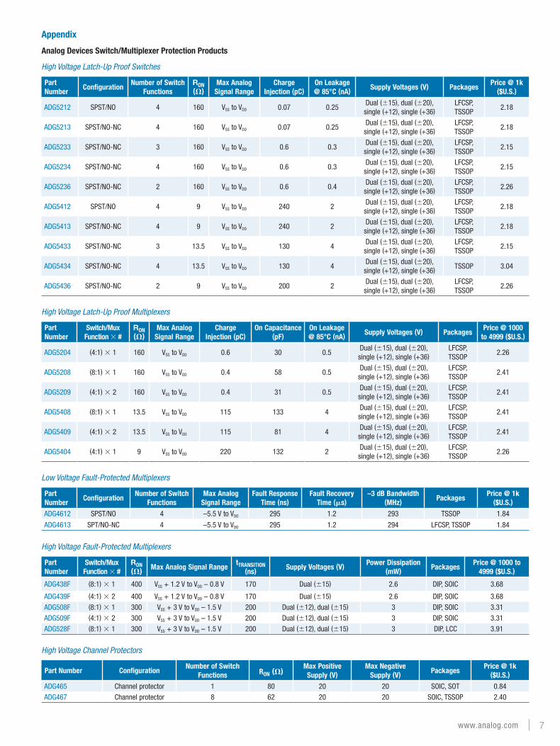
Appendix
Analog Devices Switch/Multiplexer Protection Products
High Voltage Latch-Up Proof Switches
Part Number
ConfigurationNumber of Switch
FunctionsRON (𝛀)
Max Analog Signal Range
Charge Injection (pC)
On Leakage @ 85°C (nA) Supply Voltages (V) Packages
Price @ 1k ($U.S.)
ADG5212 SPST/NO 4 160 VSS to VDD 0.07 0.25Dual (±15), dual (±20), single (+12), single (+36)
LFCSP, TSSOP
2.18
ADG5213 SPST/NO-NC 4 160 VSS to VDD 0.07 0.25Dual (±15), dual (±20), single (+12), single (+36)
LFCSP, TSSOP
2.18
ADG5233 SPST/NO-NC 3 160 VSS to VDD 0.6 0.3 Dual (±15), dual (±20), single (+12), single (+36)
LFCSP, TSSOP
2.15
ADG5234 SPST/NO-NC 4 160 VSS to VDD 0.6 0.3 Dual (±15), dual (±20), single (+12), single (+36)
LFCSP, TSSOP
2.15
ADG5236 SPST/NO-NC 2 160 VSS to VDD 0.6 0.4Dual (±15), dual (±20), single (+12), single (+36)
LFCSP, TSSOP
2.26
ADG5412 SPST/NO 4 9 VSS to VDD 240 2Dual (±15), dual (±20), single (+12), single (+36)
LFCSP, TSSOP
2.18
ADG5413 SPST/NO-NC 4 9 VSS to VDD 240 2Dual (±15), dual (±20), single (+12), single (+36)
LFCSP, TSSOP
2.18
ADG5433 SPST/NO-NC 3 13.5 VSS to VDD 130 4Dual (±15), dual (±20), single (+12), single (+36)
LFCSP, TSSOP
2.15
ADG5434 SPST/NO-NC 4 13.5 VSS to VDD 130 4Dual (±15), dual (±20), single (+12), single (+36) TSSOP 3.04
ADG5436 SPST/NO-NC 2 9 VSS to VDD 200 2Dual (±15), dual (±20), single (+12), single (+36)
LFCSP, TSSOP
2.26
High Voltage Latch-Up Proof Multiplexers
Part Number
Switch/Mux Function × #
RON (𝛀)
Max Analog Signal Range
Charge Injection (pC)
On Capacitance (pF)
On Leakage @ 85°C (nA) Supply Voltages (V) Packages
Price @ 1000 to 4999 ($U.S.)
ADG5204 (4:1) × 1 160 VSS to VDD 0.6 30 0.5Dual (±15), dual (±20), single (+12), single (+36)
LFCSP, TSSOP
2.26
ADG5208 (8:1) × 1 160 VSS to VDD 0.4 58 0.5Dual (±15), dual (±20), single (+12), single (+36)
LFCSP, TSSOP
2.41
ADG5209 (4:1) × 2 160 VSS to VDD 0.4 31 0.5 Dual (±15), dual (±20), single (+12), single (+36)
LFCSP, TSSOP
2.41
ADG5408 (8:1) × 1 13.5 VSS to VDD 115 133 4Dual (±15), dual (±20), single (+12), single (+36)
LFCSP, TSSOP
2.41
ADG5409 (4:1) × 2 13.5 VSS to VDD 115 81 4Dual (±15), dual (±20), single (+12), single (+36)
LFCSP, TSSOP
2.41
ADG5404 (4:1) × 1 9 VSS to VDD 220 132 2Dual (±15), dual (±20), single (+12), single (+36)
LFCSP, TSSOP
2.26
Low Voltage Fault-Protected Multiplexers
Part Number
Configuration Number of Switch
FunctionsMax Analog
Signal RangeFault Response
Time (ns)Fault Recovery
Time (𝛍s)–3 dB Bandwidth
(MHz) PackagesPrice @ 1k
($U.S.)
ADG4612 SPST/NO 4 –5.5 V to VDD 295 1.2 293 TSSOP 1.84
ADG4613 SPT/NO-NC 4 –5.5 V to VDD 295 1.2 294 LFCSP, TSSOP 1.84
High Voltage Fault-Protected Multiplexers
Part Number
Switch/Mux Function × #
RON (𝛀) Max Analog Signal Range
tTRANSITION (ns) Supply Voltages (V) Power Dissipation
(mW) PackagesPrice @ 1000 to
4999 ($U.S.)
ADG438F (8:1) × 1 400 VSS + 1.2 V to VDD – 0.8 V 170 Dual (±15) 2.6 DIP, SOIC 3.68
ADG439F (4:1) × 2 400 VSS + 1.2 V to VDD – 0.8 V 170 Dual (±15) 2.6 DIP, SOIC 3.68
ADG508F (8:1) × 1 300 VSS + 3 V to VDD – 1.5 V 200 Dual (±12), dual (±15) 3 DIP, SOIC 3.31
ADG509F (4:1) × 2 300 VSS + 3 V to VDD – 1.5 V 200 Dual (±12), dual (±15) 3 DIP, SOIC 3.31
ADG528F (8:1) × 1 300 VSS + 3 V to VDD – 1.5 V 200 Dual (±12), dual (±15) 3 DIP, LCC 3.91
High Voltage Channel Protectors
Part Number ConfigurationNumber of Switch
Functions RON (𝛀)Max Positive
Supply (V)Max Negative
Supply (V) PackagesPrice @ 1k
($U.S.)
ADG465 Channel protector 1 80 20 20 SOIC, SOT 0.84
ADG467 Channel protector 8 62 20 20 SOIC, TSSOP 2.40
www.analog.com | 7
www.analog.com
Analog Devices, Inc.Worldwide HeadquartersAnalog Devices, Inc. One Technology Way P.O. Box 9106 Norwood, MA 02062-9106 U.S.A. Tel: 781.329.4700 (800.262.5643, U.S.A. only) Fax: 781.461.3113
Analog Devices, Inc. Europe HeadquartersAnalog Devices, Inc. Wilhelm-Wagenfeld-Str. 6 80807 Munich Germany Tel: 49.89.76903.0 Fax: 49.89.76903.157
Analog Devices, Inc. Japan HeadquartersAnalog Devices, KK New Pier Takeshiba South Tower Building 1-16-1 Kaigan, Minato-ku, Tokyo, 105-6891 Japan Tel: 813.5402.8200 Fax: 813.5402.1064
Analog Devices, Inc. Southeast Asia HeadquartersAnalog Devices 22/F One Corporate Avenue 222 Hu Bin Road Shanghai, 200021 China Tel: 86.21.2320.8000 Fax: 86.21.2320.8222
©2011 Analog Devices, Inc. All rights reserved. Trademarks and registered trademarks are the property of their respective owners.
Printed in the U.S.A. T09923-0-11/11