SWD Interface AN1011: Standalone Programmer via the … · ... and Happy Gecko are a part of the...
33
AN1011: Standalone Programmer via the SWD Interface This application note describes a standalone programmer to program the internal flash and user page of EFM32 Gecko, Series 0 and 1, EZR32 Ser- ies 0, and EFR32 Wireless Gecko Series 1 devices that use the Serial Wire Debug (SWD) interface. Details on how to use the SWD interface to program device can be found in AN0062: Programming Internal Flash over the Serial Wire Debug Interface. This document focuses on how to optimize the process when programming the devices. The objectives of a standalone programmer are low cost, easy to build, simple to use and no PC connection is required. For simplicity, EFM32 Wonder Gecko, Gecko, Giant Gecko, Leopard Gecko, Tiny Gecko, Zero Gecko, and Happy Gecko are a part of the EFM32 Gecko Series 0. EZR32 Wonder Gecko, Leopard Gecko, and Happy Gecko are a part of the EZR32 Wireless MCU Series 0. EFM32 Pearl Gecko and Jade Gecko (and future devices) are a part of the EFM32 Gecko Series 1. EFR32 Blue Gecko, Flex Gecko, and Mighty Gecko are a part of the EFR32 Wireless Gecko Series 1. KEY POINTS • The Serial Wire Debug (SWD) interface is a two-wire interface used by Silicon Labs EFM32 Gecko, EZR32, and EFR32 Wireless Gecko devices. • The programmer writes directly to the target device Memory System Controller (MSC) registers over the SWD interface. • Future Silicon Labs EFM32/ EFR32/EZR32 devices can be easily added to the programmer. silabs.com | Smart. Connected. Energy-friendly. Rev. 0.1
Transcript of SWD Interface AN1011: Standalone Programmer via the … · ... and Happy Gecko are a part of the...

AN1011: Standalone Programmer via theSWD Interface
This application note describes a standalone programmer to program theinternal flash and user page of EFM32 Gecko, Series 0 and 1, EZR32 Ser-ies 0, and EFR32 Wireless Gecko Series 1 devices that use the SerialWire Debug (SWD) interface.Details on how to use the SWD interface to program device can be found in AN0062: ProgrammingInternal Flash over the Serial Wire Debug Interface. This document focuses on how to optimize theprocess when programming the devices.
The objectives of a standalone programmer are low cost, easy to build, simple to use and no PCconnection is required.
For simplicity, EFM32 Wonder Gecko, Gecko, Giant Gecko, Leopard Gecko, Tiny Gecko, ZeroGecko, and Happy Gecko are a part of the EFM32 Gecko Series 0.
EZR32 Wonder Gecko, Leopard Gecko, and Happy Gecko are a part of the EZR32 Wireless MCUSeries 0.
EFM32 Pearl Gecko and Jade Gecko (and future devices) are a part of the EFM32 Gecko Series 1.
EFR32 Blue Gecko, Flex Gecko, and Mighty Gecko are a part of the EFR32 Wireless Gecko Series1.
KEY POINTS
• The Serial Wire Debug (SWD)interface is a two-wireinterface used by Silicon LabsEFM32 Gecko, EZR32, andEFR32 Wireless Geckodevices.
• The programmer writesdirectly to the target deviceMemory System Controller(MSC) registers over the SWDinterface.
• Future Silicon Labs EFM32/EFR32/EZR32 devices can beeasily added to theprogrammer.
silabs.com | Smart. Connected. Energy-friendly. Rev. 0.1
1. Hardware Overview
The standalone programmer reads binary data from a Mass Storage Device (MSD) and stores it to the external EBI NAND Flash or SPINOR Flash for device programming. The programmer uses GPIO to emulate the Serial Wire Debug (SWD) interface to program thetarget device. The user interface is handled by push buttons, LEDs and LCD module.
External MemoryNAND/NOR Flash
Mass Storage Device (MSD)
LEDs and LCD Module
Push Buttons
Standalone Programmer
PC Terminal Program
USB
EBI/SPI
UARTGPIO & SPI
GPIO Target Device with SWD Interface
GPIO
Figure 1.1. Block Diagram of Standalone Programmer
1.1 Hardware Platform
There is a compile option to select the hardware platform for the standalone programmer. The programming firmware supports twohardware topologies: one which is based on the STK boards, and the other which is based on a custom hardware design. These aredescribed in the following sections.
This package can be found on the Silicon Labs website (www.silabs.com/32bit-appnotes) or within Simplicity Studio using the [Applica-tion Notes] tile.
AN1011: Standalone Programmer via the SWD InterfaceHardware Overview
silabs.com | Smart. Connected. Energy-friendly. Rev. 0.1 | 1

1.1.1 EFM32 STK
The EFM32GG_STK3700 and EFM32WG_STK3800 can be used as the EFM32 STK hardware platform of the standalone program-mer.• Handy, plug and run: no host PC is required.• On board SEGGER JLink debugger and USB virtual COM port (CDC).• Supports USB host, and MCU can run up to 48 MHz.• Onboard 32 MB NAND Flash can be used to store the binary image.• The upper 512 KB internal flash of EFM32GG990F1024 on EFM32GG_STK3700 can also be used as cache to speed up the pro-
gramming process.• Minimal hardware is required to build the programmer.
Table 1.1. Resources of EFM32 STK Used by Programmer
GPIO Signal Function
PB9 UIF_PB0 Push button 0 (PB0)
PB10 UIF_PB1 Push button 1 (PB1)
PB13 HFXTAL_P 48 MHz crystal
PB14 HFXTAL_N 48 MHz crystal
PB15 NAND_PWR_EN NAND flash power enable
PC1 NAND_ALE NAND flash address latch enable
PC2 NAND_CLE NAND flash command latch enable
PD13 NAND_WP# NAND flash write protect
PD14 NAND_CE# NAND flash chip enable
PD15 NAND_R/B# NAND flash ready/busy
PE0 (UART0#1) EFM_BC_TX Serial port TX (optional)
PE2 UIF_LED0 LED0
PE3 UIF_LED1 LED1
PE8-15 NAND_IO0-7 NAND flash 8 bit data bus
PF0 DBG_SWCLK Debug SWCLK
PF1 DBG_SWDIO Debug SWDIO
PF5 EFM_USB_VBUSEN USB 5V VBUS enable
PF6 EFM_USB_OC_FAULT USB over current detect (optional)
PF7 EFM_BC_EN Virtual COM port enable (optional)
PF8 NAND_WE# NAND flash write enable
PF9 NAND_RE# NAND flash read enable
PF10 EFM_USB_DM USB D-
PF11 EFM_USB_DP USB D+
AN1011: Standalone Programmer via the SWD InterfaceHardware Overview
silabs.com | Smart. Connected. Energy-friendly. Rev. 0.1 | 2

The 20-pin expansion header (P100) of EFM32 STK is used to connect target device and optional SPI LCD module.
Table 1.2. Expansion Header for External Hardware and Target Device
Expansion Header Pin Number Signal Function
1 GND Target device GND
2 VMCU Target device VDD
4 PD0 (USART1#1) SPI LCD module MOSI (optional)
6 PD1 (USART1#1) SPI LCD module MISO (optional)
7 PC4 Target device SWCLK
8 PD2 (USART1#1) SPI LCD module CLK (optional)
9 PC5 Target device SWDIO
12 PD4 Target device RESET
13 PB12 SPI LCD module RESET (optional)
16 PD6 SPI LCD module CS (optional)
20 3V3 SPI LCD module backlight supply (optional)
AN1011: Standalone Programmer via the SWD InterfaceHardware Overview
silabs.com | Smart. Connected. Energy-friendly. Rev. 0.1 | 3

1.1.2 Customized Hardware
Alternatively, the EFM32WG332F64/128/256 and EFM32GG332F1024 devices can be used on a custom hardware platform to imple-ment the standalone programmer.• PCB layout is required.• Supports USB host, and MCU can run up to 48 MHz.• Low pin count 4 MB SPI NOR Flash can be used to store the binary image.• The upper 512 KB internal flash of EFM32GG332F1024 can be used as a cache to speed up the programming process.• Supports the option to configure it as a gang programmer to program up to 4 or 8 devices sequentially.
Table 1.3. Pin Assignments of Customized Hardware
GPIO Signal Function
PA4 TARGET_SWC Target device SWCLK
PA5 TARGET_SWD Target device SWDIO
PB7 LFXTAL_P 32768 Hz crystal (reserve)
PB8 LFXTAL_N 32768 Hz crystal (reserve)
PB13 HFXTAL_P 48 MHz crystal
PB14 HFXTAL_N 48 MHz crystal
PC0 (I2C0#4) I2C_SDA I2C interface (reserve)
PC1 (I2C0#4) I2C_SCL I2C interface (reserve)
PC2 (USART2#0) UART_TX Serial port TX (optional)
PC3 (USART2#0) UART_RX Serial port RX (reserve)
PC4 TARGET_RESET Target device RESET
PC6 GANG4_SELECT Select x4 gang programmer mode
PC7 GANG8_SELECT Select x8 gang programmer mode
PC8 UIF_PB0 Push button 0 (PB0)
PC9 UIF_PB1 Push button 1 (PB1)
PD0 (USART1#1) FLASH_MOSI SPI Flash MOSI
PD1 (USART1#1) FLASH_MISO SPI Flash MISO
PD2 (USART1#1) FLASH_CLK SPI Flash CLK
PD3 (USART1#1) FLASH_CS SPI Flash CS
PD5 MUX_A MUX select A
PD6 MUX_B MUX select B
PD7 MUX_C MUX select C
PD8 MUX_OE MUX output enable
PE9 LCD_RESET SPI LCD module RESET
PE10 (USART0#0) LCD_MOSI SPI LCD module MOSI
PE11 (USART0#0) LCD_MISO SPI LCD module MISO
PE12 (USART0#0) LCD_CLK SPI LCD module CLK
PE13 (USART0#0) LCD_CS SPI LCD module CS
PE14 UIF_LED0 LED0
AN1011: Standalone Programmer via the SWD InterfaceHardware Overview
silabs.com | Smart. Connected. Energy-friendly. Rev. 0.1 | 4

GPIO Signal Function
PE15 UIF_LED1 LED1
PF0 DBG_SWCLK Debug SWCLK
PF1 DBG_SWDIO Debug SWDIO
PF2 USB_OC_FAULT USB over current detect (optional)
PF5 USB_VBUSEN USB 5V VBUS enable
PF10 USB_DM USB D-
PF11 USB_DP USB D+
The reference schematic of the customized hardware platform is in the “sch” folder of this application note software package.
1.2 Memory for Binary Image Storage
There is a compile option to select EBI NAND flash or SPI NOR flash for the binary image storage.
1.2.1 EBI NAND Flash
The on board NAND256W3A NAND flash is organized as 512 bytes per page, 32 pages (16 KB) per block, with the total memory sizeof 2048 blocks (32 MB). The NAND flash is accessed by the External Bus Interface (EBI) of EFM32GG or EFM32WG.
If the binary image is not a multiple of the flash page size (512 bytes), the remaining bytes are padded with 0xFF to keep the programimage aligned with the flash page.
Table 1.4. EBI NAND Flash Memory Map
Data Block Page Size Remark
Main flash image 0 – 127 0 – 4095 2048 kB Maximum 1 MB for existing micro-controller
Reserve for future expansion 128 – 2042 4096 – 65375 30640 kB Reserve for future microcontroller >2MB
User flash image 2043 65376 – 65407 16 kB Maximum 2 KB for existing micro-controller
Main flash program information 2044 65408 – 65439 16 kB File name, Start address and Lockselection
Main flash image information 2045 65440 – 65471 16 kB Main flash image size and CRC16
User page program information 2046 65472 – 65503 16 kB File name and Start address
User page image information 2047 65504 – 65535 16 kB User page image size and CRC16
AN1011: Standalone Programmer via the SWD InterfaceHardware Overview
silabs.com | Smart. Connected. Energy-friendly. Rev. 0.1 | 5

1.2.2 SPI NOR Flash
The selected SPI NOR flash is organized as 256 bytes per page, 4 KB (16 pages) per sector, 64 KB per block and total memory size is1024 sectors or 64 blocks (4 MB). The SPI flash must support 4 KB sector erase on the entire device, for example, the MacronixMX25L3206E or Cypress/Spansion S25FL132K. The SPI NOR flash is accessed by the SPI interface (USART) of EFM32GG orEFM32WG.
If the binary image is not a multiple of the flash page size (256 bytes), the remaining bytes are padded with 0xFF to keep the programimage aligned with the flash page.
Table 1.5. SPI NOR Flash Memory Map
Data Address Size Remark
Main flash image 0x00000000 – 0x001FFFFF 2048 kB Maximum 1024 kB for existing microcontroller
Reserve for future expansion 0x00200000 – 0x003FCFFF 2036 kB Reserve for future microcontroller >2 MB
User flash image 0x003FD000 – 0x003FEFFF 8 kB Maximum 2 kB for existing microcontroller
Main flash program information 0x003FF000 – 0x003FF3FF 1 kB File name, Start address and Lock selection
Main flash image information 0x003FF400 – 0x003FF7FF 1 kB Main flash image size and CRC16
User page program information 0x003FF800 – 0x003FFBFF 1 kB File name and Start address
User page image information 0x003FFC00 – 0x003FFFFF 1 kB User page image size and CRC16
1.2.3 Cache
To eliminate the read access from external memory, the programmer uses internal flash memory on the MCU to cache the main flashimage from external memory if the image size is less than or equal to 512 kB.
This feature is available on a programmer equipped with 1 MB flash EFM32 Giant Gecko. The lower 512 kB flash is used for the pro-grammer firmware whereas the upper 512 kB flash is available for the target firmware image cache.
1.3 USB Interface
The EFM32 is configured as a USB Host and is designed to communicate with a Mass Storage Device (MSD) USB class (e.g. memorystick).
1.4 LCD Module
The selected LCD module should be controlled by SPI and operated on 3.3 V. The current implementation is 4 x 20 dot matrix LCDmodule with a Solomon Systech SSD1803 LCD controller and driver.
1.5 Serial Port
When DEBUG_USB_API is turned on and USER_PUTCHAR is defined, useful debugging information will be output on the serial port. Compil-ing with the DEBUG_EFM_USER flag will also enable all asserts in both emlib and in the USB stack. If asserts are enabled and USER_PUTCHAR defined, assert texts will be output on the serial port.
The serial port can also be used as a display interface when the LCD module is not available. The serial TX data is routed to the STKvirtual COM port by setting the EFM_BC_EN line high.
1.6 Gang Programmer Mode
The gang programmer mode is available when using a custom hardware platform design. The DIP switch is used to select x1, x4 or x8operation mode. Four 1-of-8 FET Multiplexers (for example, Texas Instruments SN74CB3Q3251) are used to route the required signalsto different sockets for target device programming.
AN1011: Standalone Programmer via the SWD InterfaceHardware Overview
silabs.com | Smart. Connected. Energy-friendly. Rev. 0.1 | 6

2. Software Overview
This section covers the software drivers required for the standalone programmer.
The related software modules are found under the Simplicity Studio installation path. Example default locations on Windows for Simplic-ity Studio V3.3 are:
C:\SiliconLabs\SimplicityStudio\v3\developer\sdks\efm32\v2\usb\src
C:\SiliconLabs\SimplicityStudio\v3\developer\sdks\efm32\v2\kits\common\drivers
C:\SiliconLabs\SimplicityStudio\v3\developer\sdks\efm32\v2\reptile\fatfs
C:\SiliconLabs\SimplicityStudio\v3\developer\sdks\efm32\v2\kits\EFM32GG_STK3700\examples\nandflash
2.1 USB Host
The programmer uses the USB host stack in the “usb\src” directory and the MSD modules in the “drivers” directory to implementsupport for Mass Storage Device.
The FAT support for MSD is provided by fatfs in the “reptile\fatfs” directory.
2.2 LCD Module
The SPI LCD driver is used to retarget the printf() function to the LCD module and the retargetio.c file resides in the “drivers”directory is required.
2.3 Serial Port
The serial port driver is modified from the retargetserial.c file in “drivers” directory. It is used to retarget the printf() function tothe serial TX. The retargetio.c file resides in the “drivers” directory is required.
AN1011: Standalone Programmer via the SWD InterfaceSoftware Overview
silabs.com | Smart. Connected. Energy-friendly. Rev. 0.1 | 7

2.4 Upload Image
The programmer acts a USB host that can connect to a Mass Storage Device (MSD) such as a memory stick. The programmer search-es for a “proginfo.txt” file in the root directory of the USB MSD which contains the filename of the binary image. The programmerthen opens the binary file in root directory and reads the firmware image from the MSD and copies it to the external memory and cache(if available) for programming the target device.
The NAND flash driver is modified from the “nandflash” example of the EFM32GG_STK3700 STK.
The SPI NOR flash driver is used to erase the flash page, read data from the flash page and write data to the flash page.
AN1011: Standalone Programmer via the SWD InterfaceSoftware Overview
silabs.com | Smart. Connected. Energy-friendly. Rev. 0.1 | 8

Upload image start
Timeout?Valid USB MSD?
Proginfo.txt & corresponding binary file
in USB MSD?
Upload image from USB MSD to external
memory
External memory& cache (if available)
image checksumverify OK?
Wait key press to exit or continue
USB MSD remove?
Upload image end
USB MSD plug in?
Upload image end
Save image from external memory to cache (if available)
Save program and file information to external memoryWait key press toexit or continuue
NO
NO
YES
NO
YESYES
NONO
YES
YES
NO
YES
Figure 2.1. Upload Image Flowchart
AN1011: Standalone Programmer via the SWD InterfaceSoftware Overview
silabs.com | Smart. Connected. Energy-friendly. Rev. 0.1 | 9

2.5 Program Target Device
There are two main strategies that can be used when programming the target device. The first option is to write directly to the targetdevice’s Memory System Controller (MSC) registers over the Serial Wire Debug (SWD) interface.
The second option is to first write a program directly to target device’s RAM and then let this program control the MSC registers. Such aprogram is called a flash-loader.
Program by writing directly to MSC registers is chosen in this application note since this method is simple and easy to upgrade to sup-port new target devices. Through optimizations on flash erase and write operations, the program speed is close to the flash-loader ap-proach.
See "AN0062: Programming Internal Flash over the Serial Wire Debug Interface” for more information on how to access the debuginterface of the target device and how to use this interface to program devices.
2.5.1 Bit-Bang
The major overhead on writing directly to MSC registers method is to emulate the SWDIO and SWCLK signals by bit-banging GPIOpins. In order to speed up this process, the GPIOs of SWCLK and SWDIO for the target device must on the same GPIO port group (0-7or 8-15). The target RESET line and other signals should not be connected to this port since the software writes to the entire port atonce when bit-banging the SWCLK and SWDIO signals.
The functions readMem() and writeMem() in utils.c source file are used to read or write one 32-bit word from or to the target device’sregisters or memory.
Table 2.1. Read and Write on Accessing Target Device Register or Memory
Function Simplicity IDE Optimization –O0 Simplicity IDE Optimization –O3
readMem() 170.9 – 177.8 µs 64.6 - 66.5 µs
writeMem() 101.8-102.3 µs 29.8 – 30 µs
2.5.2 Flash Erase
There are three ways to erase the flash of the target device:
Page Erase• A page erase can be initiated from software using ERASEPAGE in MSC WRITECMD register. The page erase operations require
that the address is written into the MSC ADDRB register.
Mass Erase (Not Supported on EFM32 Gecko and EFM32 Tiny Gecko)• A mass erase can be initiated from software using ERASEMAIN0 and ERASEMAIN1 in MSC WRITECMD register. The ERASE-
MAIN0 is to erase the entire flash or lower half of the flash if device supports read-while-write. The ERASEMAIN1 is to erase theupper half of the flash if device supports read-while-write.
Device Erase• Device erase is issued over the Authentication Access Port (AAP) interface and erases all flash, SRAM, the Lock Bit (LB) page, and
the User data page Lock Word (ULW). This method is not used in this application note.
AN1011: Standalone Programmer via the SWD InterfaceSoftware Overview
silabs.com | Smart. Connected. Energy-friendly. Rev. 0.1 | 10

Table 2.2. Device Flash Organization and Erase Timing
Device Max FlashSize (kB)
Flash PageSize (Bytes)
User PageSize (Bytes)
Page Erase Page Erase Time MassErase Mass Erase-Time
EFM32G 128 512 512 Y 20 - 20.8 ms (1 page)
5.12 – 5.32 s (device)
N NA
EFM32TG 32 512 512 Y 20 - 20.8 ms (1 page)
1.28 – 1.33 s (device)
N NA
EFM32ZG 32 1024 1024 Y 20 - 20.8 ms (1 page)
0.64 – 0.66 s (device)
Y 20 - 20.8 ms
EFM32HG
EZR32HG
64 1024 1024 Y 20 - 20.8 ms (1 page)
1.28 – 1.33 s (device)
Y 20 - 20.8 ms
EFM32LGEFM32WG
EZR32LGEZR32WG
256 2048 2048 Y 20 - 20.8 ms (1 page)
2.56 – 2.66 s (device)
Y 20 - 20.8 ms
EFM32GG 1024 4096 2048 Y 20 - 20.8 ms (1 page)
5.12 – 5.32 s (device)
Y 20 - 20.8 msPer 512 KB
EFM32JGEFM32PGEFR32xG
256 2048 2048 Y 20 – 40 ms (1 page)
2.56 – 5.12 s (device)
Y 20 – 40 ms
The flash erase timing (page and mass erase) is grouped into two categories.• Page and mass erase time is 20-20.8ms
EFM32 Gecko Series 0 and EZR32 Series 0 devices (variable newFamily = false).• Page and mass erase time is 20-40ms
EFM32 Gecko Series 1 and EFR32 Wireless Gecko Series 1 devices (variable newFamily = true).
To reduce time for flash erase process, the programmer should avoid erasing the target main flash page by page especially for deviceswith larger flash memories and smaller page sizes. The EFM32 Gecko and EFM32 Tiny Gecko do not support mass erase so theirdevice flash erase operation is time consuming.
AN1011: Standalone Programmer via the SWD InterfaceSoftware Overview
silabs.com | Smart. Connected. Energy-friendly. Rev. 0.1 | 11

Flash erase start
Erase flash page by page
Flash erase end
Flash erase end
Binary image >512 KB?
Use ERASEMAIN1 to erase upper 512 KB
Use ERASEMAIN0 to erase entire flash or
lower 512 KB
Enable double writes if target is GG
NO
YES
NO
YES
Start address != 0 orTarget device is G/TG?
Figure 2.2. Flash Erase Flowchart
AN1011: Standalone Programmer via the SWD InterfaceSoftware Overview
silabs.com | Smart. Connected. Energy-friendly. Rev. 0.1 | 12

2.5.3 Combine Bootloader with Application Binary File
The mass erase can only be used on an application binary image with start address equal to 0x00000000.
There are cases the program start address is not 0x00000000 and the time-consuming page erase process must be used.
• Keep the pre-programmed bootloader and program the application firmware on a flash page size boundary address.• Program the bootloader at 0x00000000, then program the application firmware on a flash page size boundary address.
The solution is to combine the bootloader and application firmware into one binary file so the program start address can be set to0x00000000 for mass erase.
To achieve this, it needs a tool called Simplicity Commander, installed along with Simplicity Studio in a subfolder of the install folder (C:\SiliconLabs\SimplicityStudio\v3\SimplicityCommander). See UG162: “Simplicity Commander Reference Guide” for more infor-mation.
Extract the Simplicity Commander from Commander_pkg_0.14.0.zip to the current folder or another folder (e.g. C:\SiliconLabs\Simplicity Commander) to execute the command line interface.
Connect any EFM32 STK with enough flash memory for the bootloader firmware to a PC, invoke the Command-Line Interface (CLI) ofSimplicity Commander. To execute the command of Simplicity Commander, start a Windows command window and change to the Sim-plicity Commander directory (e.g. C:\SiliconLabs\Simplicity Commander).
For simplicity, put all related binary files in the Simplicity Commander directory and execute a mass erase for the device on the STK.
> commander device masserase
Flash the bootloader image (e.g. bootloader-giantgecko.bin from AN0003) to the target device, starting at 0x00000000.
> commander flash bootloader-giantgecko.bin --address 0x0
Read the flash contents from 0x0 to the start address of the application firmware (e.g. 0x1000, which must align with a target deviceflash page size boundary) and store it to a binary file (e.g. giantbl4k.bin).
The address range is non-inclusive, meaning that all bytes from 0x0 up to and including 0xFFF are read out.
> commander readmem –-range 0x0:0x1000 --outfile giantbl4k.bin
The entire flash was erased before program the bootloader image so the gap between bootloader and application firmware is filled with0xFF.
Use the MSDOS copy command to combine output binary file (giantbl4k.bin) and application firmware (e.g. giantapp.bin).
> copy giantbl4k.bl.bin/b + giantapp.bin/b ggblapp.bin/b
The combined binary file (ggblapp.bin) can now be used for device programming with program start address at 0x00000000.
AN1011: Standalone Programmer via the SWD InterfaceSoftware Overview
silabs.com | Smart. Connected. Energy-friendly. Rev. 0.1 | 13

Figure 2.3. Use Simplicity Commander to Combine Bootloader and Application Binary File
AN1011: Standalone Programmer via the SWD InterfaceSoftware Overview
silabs.com | Smart. Connected. Energy-friendly. Rev. 0.1 | 14

2.5.4 Flash Write
The write operation requires the address to be written into the MSC ADDRB register. After each 32 bit word is written, the internal ad-dress register will be incremented automatically by 4 (except EFM32 Gecko family). When a word is written to the MSC WDATA regis-ter, the WDATAREADY bit of the MSC STATUS register is cleared. When this status bit is set, software can write the next word.
The EFM32 Giant Gecko devices have the ability to do double writes to the flash. This is enabled by setting the WDOUBLE bit in theMSC WRITECTRL register, and only has effect on the main pages of the flash. When double writes are enabled, MSC WDATA acceptstwo 32-bit words before a flash write is started.
Table 2.3. Device Flash Write Features and Timing
Device Max Flash Size (kB) Auto Address In-crement
Double Words (64bit) Write
Write Time (32/64bit word)
Total Write Time
EFM32G 128 N N20 µs (min) 0.66 s
EFM32TG 32 Y N 20 µs (min) 0.16 s
EFM32ZG 32 Y N 20 µs (min) 0.16 s
EFM32HG
EZR32HG
64 Y N 20 µs (min) 0.33 s
EFM32LGEFM32WG
EZR32LGEZR32WG
256 Y N 20 µs (min) 1.31 s
EFM32GG 1024 Y Y (Main flash only) 20 µs (min) 5.24 s (32 bit word)
2.62 s (64 bit word)
EFM32JGEFM32PG EFR32xG
256 Y N 20 – 40 µs 1.31 – 2.62 s
The flash write timing can be grouped into two categories.• Flash write time is 20 µs minimum
EFM32 Gecko Series 0 and EZR32 Series 0 devices (variable newFamily = false).• Flash write time is 20-40 µs
EFM32 Gecko Series 1 and EFR32 Wireless Gecko Series 1 devices (variable newFamily = true).
To reduce the time for the flash write process, the programmer should try to skip polling the WDATAREADY bit in MSC STATUS regis-ter after writing each 32- or 64-bit word since the register read process is time consuming (~65 µs). The alternative is to add a fixedmicro second delay between each write to make sure the maximum write time can be met. The EFM32 Gecko family does not supportauto address increment so it needs to load new address into the MSC ADDRB register prior to writing each 32 bit word.
AN1011: Standalone Programmer via the SWD InterfaceSoftware Overview
silabs.com | Smart. Connected. Energy-friendly. Rev. 0.1 | 15

Flash write start
Target flash page boundary?
Target isEFM32Gfamily?
Load new page address to target
Cache available?
Read one external memory page to
buffer
Write one word or two words (if target is GG) from buffer
or cache to target
External flash page boundary?
Skip polling?
External flash page boundary?
Cache available?
Read one external memory page to
buffer
Load new word address to target
Zero or few µs delay
WDATAREADY?
End of binary image?
Flash write end
YES
NO
YES
NO
YES
NO
NO
YESYES
NO
NO
YES
YES
NO
YES
NO
YES
NO
Figure 2.4. Flash Write Flowchart
AN1011: Standalone Programmer via the SWD InterfaceSoftware Overview
silabs.com | Smart. Connected. Energy-friendly. Rev. 0.1 | 16

2.5.5 Flash Verify
The programmer verifies the target flash contents with external memory or cache (if available) to make sure that no errors occurredduring the programming process. The auto increment of Transfer Address Register (TAR) is for burst read within TAR wrap aroundboundary, the TAR must be initialized at every TAR wrap boundary to setup the next flash read address.
AN1011: Standalone Programmer via the SWD InterfaceSoftware Overview
silabs.com | Smart. Connected. Energy-friendly. Rev. 0.1 | 17

Flash verify start
TAR wrap boundary?
Initialize new TAR
Cache available?
Read one external memory page to
buffer
Read one word from target and compare with buffer or cache
External flash page boundary?
Content match?
End of binary image?
Flash verify end
Set autoincrement on TAR
Reset autoincrement on TAR
Display error message
NO
YESYES
NO
NO
YES
NO
YES
NO
YES
Figure 2.5. Flash Verify Flowchart
AN1011: Standalone Programmer via the SWD InterfaceSoftware Overview
silabs.com | Smart. Connected. Energy-friendly. Rev. 0.1 | 18
2.5.6 Debug Access and Authentication Access Port (AAP) Access Lock
The debug access to the Cortex core is locked by clearing the Debug Lock Word (DLW, word 127) in the Lock Bits page and resettingthe device. When debug access is locked, the debugger can access the AAP registers. However, the connection to the Cortex core andthe whole bus system is blocked.
The AAP access is locked by clearing the Authentication Access Port (AAP) lock word (ALW, word 124) of the Lock Bits page. Oncethe AAP is locked, it is impossible to perform an external mass erase and the AAP lock cannot be reset. The only way to program thedevice when AAP is locked is through a bootloader or by software already loaded into the flash.
The lock feature can be grouped into two categories:• Devices support debug access lock only
EFM32 Gecko Series 0 and EZR32 Series 0 devices (variable newFamily = false).• Devices support debug access and AAP lock
EFM32 Gecko Series 1 and EFR32 Wireless Gecko Series 1 devices (variable newFamily = true).
AN1011: Standalone Programmer via the SWD InterfaceSoftware Overview
silabs.com | Smart. Connected. Energy-friendly. Rev. 0.1 | 19

2.6 Compile Options
The programmer has its corresponding header files to setup the software and hardware environment. The hardware environment isconfigured by the header files as shown in the following table, whereas the software environment is configured by the progconf.h andthe related parameters shown in the next table.
Table 2.4. Header Files for Hardware Configuration
File Usage Default Value
lcddisplay.h Define the USART and GPIO to inter-face with external LCD module
SeeTable 1.1 Resources of EFM32 STK Used by Programmeron page 2, Table 1.2 Expansion Header for External Hardwareand Target Device on page 3 and Table 1.3 Pin Assignments of
Customized Hardware on page 4 for details
spiflash.h Define the USART and GPIO to inter-face with external SPI flash
SeeTable 1.1 Resources of EFM32 STK Used by Programmeron page 2, Table 1.2 Expansion Header for External Hardwareand Target Device on page 3 and Table 1.3 Pin Assignments of
Customized Hardware on page 4 for details
kits.h Define GPIO for keys, LEDs, SWD inter-face and external MUX control
SeeTable 1.1 Resources of EFM32 STK Used by Programmeron page 2, Table 1.2 Expansion Header for External Hardwareand Target Device on page 3 and Table 1.3 Pin Assignments of
Customized Hardware on page 4 for details
vcomdisplay.h Define GPIO for serial port SeeTable 1.1 Resources of EFM32 STK Used by Programmeron page 2, Table 1.2 Expansion Header for External Hardwareand Target Device on page 3 and Table 1.3 Pin Assignments of
Customized Hardware on page 4 for details
Table 2.5. Parameters in progconf.h File for Software Configuration
Parameter Usage Default Setting
USE_EFM32_STK Use EFM32 STK or customized hardware for programmer(FALSE for customized hardware, TRUE for EFM32 STK)
TRUE
TEXT_FILENAME Define the text file name that provides the information to programthe device
proginfo.txt
EXTERNAL_MEMORY Select EBI NAND flash or SPI NOR flash (0 for SPI NOR FLASH,1 for EBI NAND Flash)
1 (EBI_NAND_FLASH)
USB_WAIT_TIMEOUT Timeout in seconds to wait until USB MSD is plugged in 5
SKIP_POLLING Skip polling the WDATAREADY bit in MSC STATUS register afterwriting data to target device flash (TRUE to skip)
TRUE
WRITE_DELAY Delay in micro seconds after writing data to target device flash(only valid if SKIP_POLLING = TRUE)
10 if using EFM32GG
11 if using EFM32WG
LOCK_RESET_DELAY Pin reset delay after debug lock in milliseconds 1
ERASE_DELAY Delay in milliseconds after a flash page erase or mass erase 20
ERASE_LOOPCNT Loop count to poll the BUSY bit in the MSC STATUS register aftera flash page erase or mass erase
400 (>20 ms)
RESET_PULSE_WIDTH Pin reset pulse width in milliseconds 1
RESET_DELAY Pin reset delay in milliseconds 1
MUX_DELAY Delay in milliseconds after swithcing external MUX control pins ingang programming mode
1
DISP_INTERFACE Select display interface ((0 for none, 1 for LCD, 2 for serial port) 2 (DISP_VCOM)
AN1011: Standalone Programmer via the SWD InterfaceSoftware Overview
silabs.com | Smart. Connected. Energy-friendly. Rev. 0.1 | 20

2.7 Add a New Silicon Labs EFM32/EFR32/EZR32 Device to the Programmer
The new Silicon Labs EFM32/EFR32/EZR32 device should have a Serial Wire Debug (SWD) interface with a Cortex-M0+, Cortex-M3or Cortex-M4 core. The known differences between current EFM32/EFR32/EZR32 families are Chip Information (Family Code…) in theDevice Information (DI) page, the Memory System Controller (MSC) Base Address, the AAP Identification Register (IDR) value if debugaccess is locked, the wrap boundary of the Transfer Address Register (TAR) on the AHB-AP, the flash erase timing (see Table2.2 Device Flash Organization and Erase Timing on page 11 for details) and the flash write timing (see Table 2.3 Device Flash WriteFeatures and Timing on page 15 for details).
Table 2.6. Differences between Current EFM32/EFR32/EZR32 Families
Device Family Code MSC Base Address IDR Value (Lock/Unlock) Wrap Boundary of TAR
EFM32G 71 0x400C0000 0x16E60001/0x24770011 0xFFF
EFM32GG 72 0x400C0000 0x16E60001/0x24770011 0xFFF
EFM32TG 73 0x400C0000 0x16E60001/0x24770011 0xFFF
EFM32LG 74 0x400C0000 0x16E60001/0x24770011 0xFFF
EFM32WG 75 0x400C0000 0x16E60001/0x24770011 0xFFF
EFM32ZG 76 0x400C0000 0x16E60001/0x04770031 0x3FF
EFM32HG 77 0x400C0000 0x16E60001/0x04770031 0x3FF
EZR32WG 120 0x400C0000 0x16E60001/0x24770011 0xFFF
EZR32LG 121 0x400C0000 0x16E60001/0x24770011 0xFFF
EZR32HG 122 0x400C0000 0x16E60001/0x04770031 0x3FF
EFM32PG 81 0x400E0000 0x26E60011/0x24770011 0xFFF
EFM32JG 83 0x400E0000 0x26E60011/0x24770011 0xFFF
EFR32MG 16-18 0x400E0000 0x26E60011/0x24770011 0xFFF
EFR32BG 19-21 0x400E0000 0x26E60011/0x24770011 0xFFF
EFR32FG 25-27 0x400E0000 0x26E60011/0x24770011 0xFFF
AN1011: Standalone Programmer via the SWD InterfaceSoftware Overview
silabs.com | Smart. Connected. Energy-friendly. Rev. 0.1 | 21

If the differences in the new device are identified, the corresponding header files and source files should be modified to support the newdevice. The parameters for software configuration in Table 2.5 Parameters in progconf.h File for Software Configuration on page 20may need to be changed to adapt to the new device. The following table is an example showing how to add EFR32MG support to theprogrammer.
Table 2.7. Header and Source Files Need to be Modified to Add a New Device
Item File Existing Define or Code Action
Family code util.h No define for EFR32MG
Add below defines to util.h
#define _DEVICE_FAMILY_EFR32MG1P 16#define _DEVICE_FAMILY_EFR32MG1B 17#define _DEVICE_FAMILY_EFR32MG1V 18
util.c
No code for EFR32MG
Note:
newFamily = false for
EFM32 Gecko Series 0 and EZR32 Series 0devices
newFamily = true for
EFM32 Gecko Series 1 and EFR32 WirelessGecko Series 1 devices
Add EFR32MG support to getDeviceName()function, use EFR32MG1P as an example
case _DEVICE_FAMILY_EFR32MG1P: sprintf(familyCode, "%s", "EFR32MG1P"); mainPageSize = 2048; userPageSize = 2048; mainPageSizeMask = 0x7ff; setMscBaseAddrP2(); newFamily = true; break;
MSC Base Ad-dress util.h #define MSCBASE_ADDR_P1 0x400c0000
#define MSCBASE_ADDR_P2 0x400e0000The MSCBASE_ADDR_P2 define can coverEFR32MG
util.h
__STATIC_INLINE void setMscBaseAddrP1(void)
__STATIC_INLINE void setMscBaseAddrP2(void)
The setMscBaseAddrP2() function can coverEFR32MG
IDR Value dap.h #define EFM32_AAP_ID_P1 0x16e60001#define EFM32_AAP_ID_P2 0x26e60011
The EFM32_AAP_ID_P2 define can coverEFR32MG
utils.c Used in checkIfMzeroIsLocked() and connectToTarget() function
The checkIfMzeroIsLocked() function is on-ly for Cortex-M0+ core
The connectToTarget() function can coverEFR32MG (EFM32_AAP_ID_P2)
debug_lock.c Used in lockTarget() function The current lockTarget() function can coverEFR32MG (EFM32_AAP_ID_P2)
Wrap Boundaryof TAR utils.h #define TAR_WRAP_4K 0xFFF
#define TAR_WRAP_1K 0x3FFThe TAR_WRAP_4K define can cover EFR32MG
utils.c No code for EFR32MG
Add EFR32MG support to getTarWrap() func-tion on return TAR_WRAP_4K;
case _DEVICE_FAMILY_EFR32MG1P: case _DEVICE_FAMILY_EFR32MG1B: case _DEVICE_FAMILY_EFR32MG1V:
Software Param-eters progconfig.h
#if defined(_EFM32_GIANT_FAMILY)#define WRITE_DELAY 10#else#define WRITE_DELAY 11#endif
Current WRITE_DEALY can support EFR32MG
AN1011: Standalone Programmer via the SWD InterfaceSoftware Overview
silabs.com | Smart. Connected. Energy-friendly. Rev. 0.1 | 22
3. User Interface
3.1 Push Buttons
There are two push buttons, PB0 and PB1, on the programmer.
PB0:• Scrolls down in main menu.• Returns to main menu from submenu.
PB1:• Executes the selected item.
3.2 LEDs
There are two LEDs, LED0 and LED1, on the programmer.
LED0:• On if an error occurs.
LED1:• On if the programmer is busy, indicating push buttons are ignored.
LED0 and LED1 are also used to display menu status if an LCD is not available for the programmer.
3.3 Display
There is compile option to select display interface for standalone programmer.
3.3.1 No Display
This is not recommended since the programmer status can only be indicated by LED0 and LED1.
3.3.2 External LCD Module
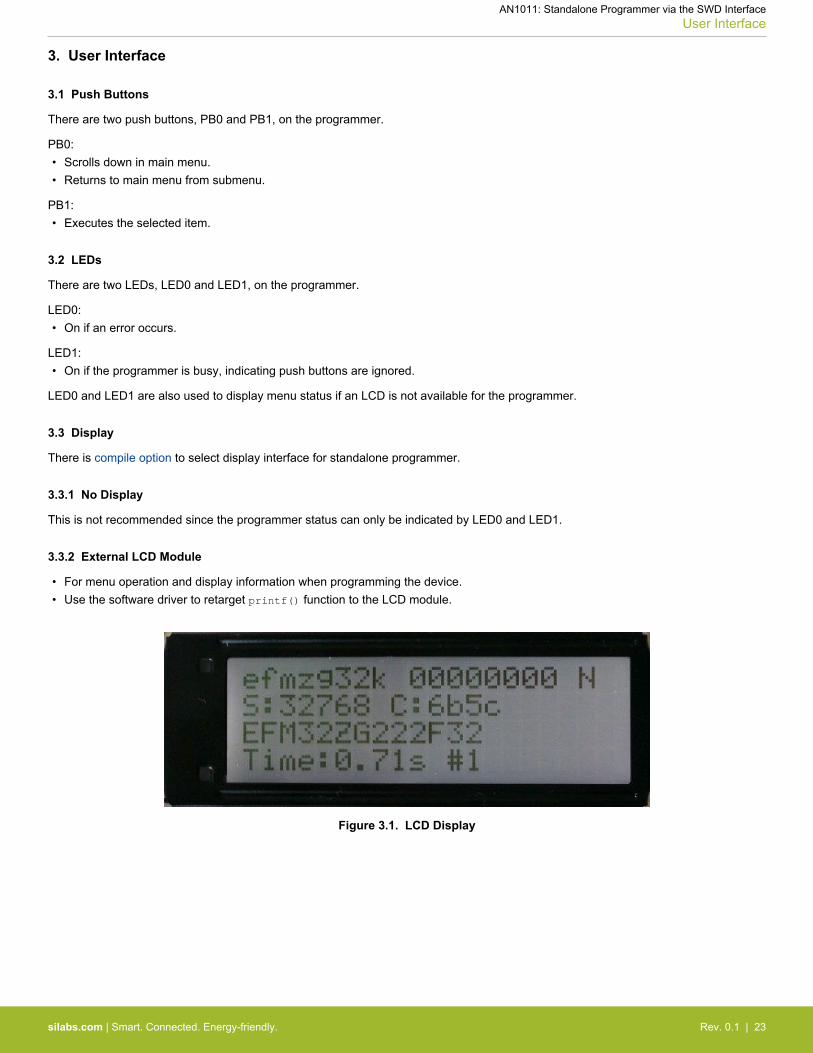
• For menu operation and display information when programming the device.• Use the software driver to retarget printf() function to the LCD module.
Figure 3.1. LCD Display
AN1011: Standalone Programmer via the SWD InterfaceUser Interface
silabs.com | Smart. Connected. Energy-friendly. Rev. 0.1 | 23

3.3.3 Serial Interface
• For debugging and menu operation if LCD is not available.• USB to UART Bridge is not required if using EFM32GG or EFM32WG STK (onboard USB virtual COM port) as programmer.• Use software driver to retarget printf() function to serial interface (115200 N 8 1).• PC terminal software is required to display data from serial interface.
Figure 3.2. Serial Interface Display
AN1011: Standalone Programmer via the SWD InterfaceUser Interface
silabs.com | Smart. Connected. Energy-friendly. Rev. 0.1 | 24
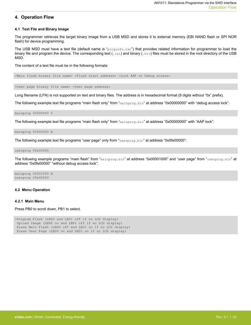
4. Operation Flow
4.1 Text File and Binary Image
The programmer retrieves the target binary image from a USB MSD and stores it to external memory (EBI NAND flash or SPI NORflash) for device programming.
The USB MSD must have a text file (default name is “proginfo.txt”) that provides related information for programmer to load thebinary file and program the device. The corresponding text (.txt) and binary (.bin) files must be stored in the root directory of the USBMSD.
The content of a text file must be in the following formats:
<Main flash binary file name> <Flash start address> <Lock AAP or Debug access>
<User page binary file name> <User page address>
Long filename (LFN) is not supported on text and binary files. The address is in hexadecimal format (8 digits without “0x” prefix).
The following example text file programs “main flash only” from “mainprog.bin” at address “0x00000000” with “debug access lock”:
mainprog 00000000 Y
The following example text file programs “main flash only” from “mainprog.bin” at address “0x00000000” with “AAP lock”:
mainprog 00000000 A
The following example text file programs “user page” only from “userprog.bin” at address “0x0fe00000”:
userprog 0fe00000
The following example programs “main flash” from “mainprog.bin” at address “0x00001000” and “user page” from “userprog.bin” ataddress “0x0fe00000” “without debug access lock”:
mainprog 00001000 N userprog 0fe00000
4.2 Menu Operation
4.2.1 Main Menu
Press PB0 to scroll down, PB1 to select.
>Program Flash (LED0 and LED1 off if no LCD display) Upload Image (LED0 on and LED1 off if no LCD display) Erase Main Flash (LED0 off and LED1 on if no LCD display) Erase User Page (LED0 on and LED1 on if no LCD display)
AN1011: Standalone Programmer via the SWD InterfaceOperation Flow
silabs.com | Smart. Connected. Energy-friendly. Rev. 0.1 | 25

4.2.2 Program Flash Submenu
This menu displays the current valid binary image information in external memory. “S:” is the binary file size in bytes, and “C:” is thebinary file checksum (CRC16) in hexadecimal.
mainprog 00000000 N S:524288 C:4196
Displays "No binary in memory" if no valid binary image is in external memory.
Press PB1 to program target, PB0 to return to main menu.
Displays the target device information, current process and LED1 turns on during operation.
EFM32GG990F1024 ERASE/PROG/VER MAIN
Displays the programing time and device count (#n) if no errors occurred during the operation.
Time:8.99s #1
Displays error message(s) if the programming fails, and also turns on LED0.
In gang programming mode, the four or eight target devices are programmed sequentially.
Press PB0 to program again, PB1 to return to main menu.
4.2.3 Upload Image Submenu
This menu starts by waiting for the user to plug the USB MSD device in.
Plug in USB MSDWait...
If a USB MSD is not detected within the timeout interval (default is 5 seconds), it will display an error code:
No device plug-in
Press PB1 to retry, PB0 to return to main menu.
Displays the binary image information similarly to the program flash submenu, if a valid binary file is successfully uploaded from USBMSD to the external memory.
mainprog 00000000 NS:524288 C:4196
Displays error message(s) if the upload image process fails.
Press PB1 to upload the image again, PB0 to return to main menu.
4.2.4 Erase Main Flash Submenu
This menu will display the target device information and turn LED1 on during the operation.
EFM32ZG222F32
Displays the following message if no error occurs during the main flash erase.
Erase Main done
Displays error message(s) and turns LED0 on if the erase main flash operation fails.
In gang program mode, the main flash of four or eight target devices are erased sequentially.
Press PB0 to erase main flash again, PB1 to return to main menu.
AN1011: Standalone Programmer via the SWD InterfaceOperation Flow
silabs.com | Smart. Connected. Energy-friendly. Rev. 0.1 | 26

4.2.5 Erase User Page Submenu
This menu displays the target device information and turns LED1 on during the operation.
EFM32ZG222F32
Displays the following message if no error occurs during the user page erase.
Erase User done
Displays error message(s) and turns LED0 on if the erase user page fails.
In gang program mode, the user page of four or eight target devices are erased sequentially.
Press PB0 to erase user page again, PB1 to return to main menu.
AN1011: Standalone Programmer via the SWD InterfaceOperation Flow
silabs.com | Smart. Connected. Energy-friendly. Rev. 0.1 | 27

5. Testing
5.1 Test Setup
The interconnection diagram used with the programmer is shown in the figure below. The programmer is the EFM32GG_STK3700 orEFM32WG_STK3800 and the target device is EFM32 STK or EFR32 WSTK or EZR32 WSTK.
ProgrammerVDD
Input_Pin
GPIO for SWDIO
GPIO for SWCLK
GPIO for RESET
Target Device
GND
VDD
SWDIO
SWCLK
RESET
GND
VDD
Figure 5.1. Programmer Connection Diagram
The corresponding signals on different target STK and WSTK are shown in the table below. The pin or pad location can be found in theschematic and assembly drawing of the associated STK or WSTK
The target device on STK or WSTK is powered by the programmer so the power switch (the slide switch in the lower left corner of theboard) of STK or WSTK should be in the BAT position.
Table 5.1. Pins or Pads for Connection on Target STK and WSTK
Target Device STK or WSTK Signal Pin or Pad on STK or WSTK MainBoard Pad on WSTK Radio Board
EFM32_Gxxx_STK
EFM32GG_STK3700
EFM32LG_STK3600
EFM32TG_STK3300
EFM32WG_STK3800
GND
RESET
SWDIO
SWCLK
VDD
TP811
TP815
TP812
TP813
Pin 2 of P100 (EXP port)
NA
SLSTK3400A_EFM32HG
GND
RESET
SWDIO
SWCLK
VDD
Pin 3 of J102
TP400
Pin 7 of J102
Pin 5 of J102
Pin 2 of P100 (EXP port)
NA
AN1011: Standalone Programmer via the SWD InterfaceTesting
silabs.com | Smart. Connected. Energy-friendly. Rev. 0.1 | 28
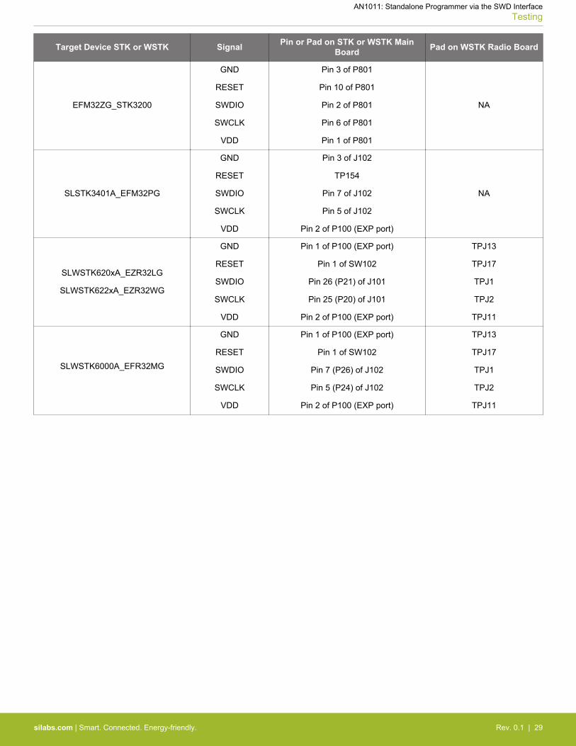
Target Device STK or WSTK Signal Pin or Pad on STK or WSTK MainBoard Pad on WSTK Radio Board
EFM32ZG_STK3200
GND
RESET
SWDIO
SWCLK
VDD
Pin 3 of P801
Pin 10 of P801
Pin 2 of P801
Pin 6 of P801
Pin 1 of P801
NA
SLSTK3401A_EFM32PG
GND
RESET
SWDIO
SWCLK
VDD
Pin 3 of J102
TP154
Pin 7 of J102
Pin 5 of J102
Pin 2 of P100 (EXP port)
NA
SLWSTK620xA_EZR32LG
SLWSTK622xA_EZR32WG
GND
RESET
SWDIO
SWCLK
VDD
Pin 1 of P100 (EXP port)
Pin 1 of SW102
Pin 26 (P21) of J101
Pin 25 (P20) of J101
Pin 2 of P100 (EXP port)
TPJ13
TPJ17
TPJ1
TPJ2
TPJ11
SLWSTK6000A_EFR32MG
GND
RESET
SWDIO
SWCLK
VDD
Pin 1 of P100 (EXP port)
Pin 1 of SW102
Pin 7 (P26) of J102
Pin 5 (P24) of J102
Pin 2 of P100 (EXP port)
TPJ13
TPJ17
TPJ1
TPJ2
TPJ11
AN1011: Standalone Programmer via the SWD InterfaceTesting
silabs.com | Smart. Connected. Energy-friendly. Rev. 0.1 | 29

5.2 Test Results
The binary files for testing are saved in the “testbin” folder of this application note and the test results in the table below are based onfollowing conditions.• SDK is EFM32 SDK v4.4.0• Erase, program and verify main flash only• Compile options of progconfig.h are set to default values (SKIP_POLLING = TRUE, WRITE_DELAY = 10 for
EFM32GG_STK3700 and WRITE_DELAY = 11 for EFM32GG_STK3800)• Software is compiled with –O3 optimization (release build) in Simplicity IDE• External memory is on board NAND flash, and internal cache is available on EFM32GG_STK3700
Table 5.2. Program Time for Different Target Devices
Target Device (STK or WSTK) Binary FileName
BinaryFile Size
Program in Bi-nary File EFM32GG_STK3700 EFM32WG_STK3800
EFM32ZG_STK3200 efmzg32k 32 KB spaceinvaders 0.71s 0.74s
EFM32TG_STK3300 efmtg32k 32 KB emlcd 2.24s 2.26s
SLSTK3400A_EFM32HG efmhg64k 64 KB spaceinvaders 1.39s 1.43s
EFM32_Gxxx_STK efmg128k 128 KB emlcd 10.7s 10.33s
EFM32LG_STK3600
EFM32WG_STK3800efm256k 256 KB emlcd 5.47s 5.62s
EFM32GG_STK3700 efm512k 512 KB emlcd 8.99s 9.34s
EFM32GG_STK3700 efm1024k 1024 KB emlcd 18.38s 18.69s
SLWSTK620xA_EZR32LG
SLWSTK622xA_EZR32WGezr256k 256 KB clock 5.47s 5.62s
SLSTK3401A_EFM32PG efr256k 256 KB spaceinvaders 6.31s 6.43s
SLWSTK6000A_EFR32MG efr256k 256 KB spaceinvaders 6.31s 6.43s
AN1011: Standalone Programmer via the SWD InterfaceTesting
silabs.com | Smart. Connected. Energy-friendly. Rev. 0.1 | 30

6. Document Revision History
Revision 0.1
July 26, 2016
Initial release.
AN1011: Standalone Programmer via the SWD InterfaceDocument Revision History
silabs.com | Smart. Connected. Energy-friendly. Rev. 0.1 | 31

http://www.silabs.com
Silicon Laboratories Inc.400 West Cesar ChavezAustin, TX 78701USA
Simplicity StudioOne-click access to MCU and wireless tools, documentation, software, source code libraries & more. Available for Windows, Mac and Linux!
IoT Portfoliowww.silabs.com/IoT
SW/HWwww.silabs.com/simplicity
Qualitywww.silabs.com/quality
Support and Communitycommunity.silabs.com
DisclaimerSilicon Labs intends to provide customers with the latest, accurate, and in-depth documentation of all peripherals and modules available for system and software implementers using or intending to use the Silicon Labs products. Characterization data, available modules and peripherals, memory sizes and memory addresses refer to each specific device, and "Typical" parameters provided can and do vary in different applications. Application examples described herein are for illustrative purposes only. Silicon Labs reserves the right to make changes without further notice and limitation to product information, specifications, and descriptions herein, and does not give warranties as to the accuracy or completeness of the included information. Silicon Labs shall have no liability for the consequences of use of the information supplied herein. This document does not imply or express copyright licenses granted hereunder to design or fabricate any integrated circuits. The products are not designed or authorized to be used within any Life Support System without the specific written consent of Silicon Labs. A "Life Support System" is any product or system intended to support or sustain life and/or health, which, if it fails, can be reasonably expected to result in significant personal injury or death. Silicon Labs products are not designed or authorized for military applications. Silicon Labs products shall under no circumstances be used in weapons of mass destruction including (but not limited to) nuclear, biological or chemical weapons, or missiles capable of delivering such weapons.
Trademark InformationSilicon Laboratories Inc.® , Silicon Laboratories®, Silicon Labs®, SiLabs® and the Silicon Labs logo®, Bluegiga®, Bluegiga Logo®, Clockbuilder®, CMEMS®, DSPLL®, EFM®, EFM32®, EFR, Ember®, Energy Micro, Energy Micro logo and combinations thereof, "the world’s most energy friendly microcontrollers", Ember®, EZLink®, EZRadio®, EZRadioPRO®, Gecko®, ISOmodem®, Precision32®, ProSLIC®, Simplicity Studio®, SiPHY®, Telegesis, the Telegesis Logo®, USBXpress® and others are trademarks or registered trademarks of Silicon Labs. ARM, CORTEX, Cortex-M3 and THUMB are trademarks or registered trademarks of ARM Holdings. Keil is a registered trademark of ARM Limited. All other products or brand names mentioned herein are trademarks of their respective holders.